discrete solution and...
TRANSCRIPT

Discrete Solution and Application:Power MOSFET and Rectifier
陳 文 聰
意法半導體大中華暨亞太區
功率元件技術行銷專案經理
Agenda
Power MOSFET
• High Voltage MOSFET
• Low Voltage MOSFET
• Silicon Carbide MOSFET
• Package
Power Rectifier
• Silicon Carbide Diodes
• FERD Diodes
• Differentiation through innovation
Flat / package size reduction
2

Power MOSFETHigh Voltage MOSFET

High Voltage Power MOSFET
SuperMESHTM K3
MDmeshTM K5
MDmeshTM M2
Planar
technology
Super-junction
technology
200V 400V 800V 1050V 1500V
PowerMESH
“N series”SuperMESH “NK series”
Motor control
Adapters
Telecom
DC-DC
Industrial
SMPS
Automotive
ServersUPS
MDmesh
1200V1000V650V 700V500V
MDmeshTM DM2 with fast diode
MDmeshTM M5
MDmeshTM
M2 EP
MDmeshTM M6
600V
MDmeshTM M6S
4

Products & Applications
SuperJunction Mdmesh™ M5, M2, M6S, M6, DM2/DM6 & K5 Technologies
M5: leading technology for
high end hard switch
Key Features
• Industry’s one of the
lower RDS(on) in the
Market
• High switching speed
• 650V BVdss rated
Benefits
• highest efficiency in the
application
• Smaller form factor of
final system
• Especially targeted for
High Power hard
switching (PFC, Boost,
TTF, Flyback)
M6/ M2 / M2 EP:
best for LLC
Key Features
• Up to 30% lower Qg
(equivalent die size)
• 400 – 700V Bvdss rated
• Back-to-Back G-S zener
protected
Benefits
• Reduced switching
losses through optimized
(Qg) (Ciss, Coss)
• Enhanced immunity vs
ESD & Vgs spikes in the
application
• Especially targeted for
HB LLC, TTF, Flyback..)
• M2 EP Tailored for Very
High Frequency
Converters (f > 150 kHz)
DM2 DM6 Fast Diode:
best F/B ZVS
Key Features
• Integrated fast body
diode
• Softer commutation
behavior
• Back-to-Back G-S zener
protected
Benefits
• Reduced switching
losses through
optimized (Qg) (Ciss,
Coss)
• High peak diode dV/dt
capabilities
• Best use in Full Bridge
ZVS
K5: best in class
Very High Voltage
Key Features
• Extremely good RDS(on)
at very high BVDSS
• High switching speed
• From 800 till 1500V
BVDSS rated
• 950 V and 1050 V
integrated fast body
diode
Benefits
• High efficiency with
lower design complexity
• Especially targeted for
flyback LED topologies
and high voltage range in
the application
M6S: improved
performance for medium
power hard switch
Key Features
• Up to 15% RDS(on)
reduction vs M2 tech.
• High switching speed
• 600V BVdss rated
Benefits
• Better efficiency in
medium Power hard
switch application
• Smaller form factor of
final system
• Especially targeted for
hard switching (PFC,
Boost, TTF, Flyback)
5

Flyback / Two
Transistors Forward
M5
400V to 700V 550V - 650V
Soft-switching
topologies LLC
resonant
Solar Inverters, UPS, HEV
Chargers /
Adapters /
SilverBox / LED
lighting
DM2
Hi-End PFC, Hard
switching topologiesZVS / FB & HF
600V- 650V
K5
Flyback
LED Driver
LED Lighting
Adapter / Metering
M6 DM6 K5 / DK5
800V 950V
1050V 1200V 1500V
M9
M2
M2-EP
Hard switching
topologies Flyback
PFC
Chargers / Adapters
/ SilverBox / LED
lighting
M6S
Server / Telecom
600V to 700V600V
Current & Next SJ Technologies Application / Topology Positioning
6

The Ideal SJ MOSFET - PFC
• Current level for a PFC both TM and CCM is linked to the load and the input voltage
• Drain current sweeps wide range
• MOSFET switching characteristics from low to medium current values should be considered for efficiency target
• High current portion has anyhow to be taken into account too for overload condition ad low input voltage
7

HV Power MOSFET Series : MDmesh V
Key Features
• Industry’s lowest RDS(on) in the market
• High switching speed
• 650V BVdss rated
Benefits
• Highest efficiency in the application
• Smaller form factor of final system
• Especially targeted for hard switching
(PFC, Boost, TTF, Flyback)
MDmesh V: the leading technology with outstandingly low RDS(on)
8

The New M2 Series vs MDmesh IIImproved RDS(on) x area
Same Production Cycle-Time
Improved Qg: -30%
Improved Ciss: -15%
Improved Coss profile vs Vds
Gate charge comparison™ – VDD=480V – ID=20A – Ig=1.3mA
STP24N60M2 190mΩ(MAX) 29nC(TYP)
First Super-Junction technology integrating Back-to-Back G-S Zeners
Enhanced immunity vs ESD & Vgs spikes
500V (280 – 530 mohm) 650V (46 mohm – 1.3 ohm)600V (40 mohm – 1.4 ohm)
9
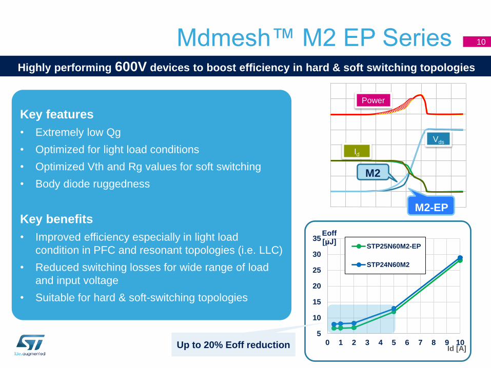
Key features
• Extremely low Qg
• Optimized for light load conditions
• Optimized Vth and Rg values for soft switching
• Body diode ruggedness
Key benefits
• Improved efficiency especially in light load
condition in PFC and resonant topologies (i.e. LLC)
• Reduced switching losses for wide range of load
and input voltage
• Suitable for hard & soft-switching topologies
Mdmesh™ M2 EP SeriesHighly performing 600V devices to boost efficiency in hard & soft switching topologies
5
10
15
20
25
30
35
0 1 2 3 4 5 6 7 8 9 10
Eoff[μЈ]
Id [A]
STP25N60M2-EP
STP24N60M2
Vds
Id
Power
M2
M2-EP
Up to 20% Eoff reduction
10

Working with a new diffusion
process and optimizing the
MDmeshTM M2 vertical structure,
the new product improves the
turn-off behavior towards the
“ideal” switch. Giving an
improved shape of the turn-off
waveforms, the new series M6
represents an evolution of the
M2 series.
Optimized
Original
Ideal
General Description 11

Main benefits
• Especially suitable for Bridge topologies • Improved intrinsic diode reverse recovery time• Higher dV/dt capabilty
• Increased power density in FB & HF(W/inch*2)
• Improved system reliability
• Higher efficiency in bridge topologies
Key Features
Key Benefits
Diode Parameters
Mx
DMx
MDmeshTM Mx
MDmeshTM DMx
DeviceRdon
(max)
(mohm)
Irm
(A)
Ta
(ns)
Tb
(ns)
S
(Tb/Ta)
TRR
(ns)
QRR
(nC)
STW56N60DM2 60 9.2 112 40 0.357 152 815
STW55NM60ND 70 17.6 184 28 0.152 212 1951
-Diode body Drain-Source-@ VR=400V, IF=50A; di/dt=100A/µs, Tc=25°C.
MDmeshTM DMx Series with Fast Recovery Diode
The perfect switch for ZVS , Half and Full bridge converters
12

Main benefits
Leading leg MOSFETs
S1 – S2
Body diode
recovery
Body
diodeMOSFET
channel
Dangerous
condition
Dangerous
condition
Application note
• AN-4720
• AN-2626
Why MOSFET with Fast Recovery Diode
13

Power MOSFETLow Voltage MOSFET

LV MOSFET - STripFET Series
H6 F6
40V - 80V
Load Switch
O-ring
Motor drives
UPS / e-Motor /e-
Bike / Toys / Fan
Control
STB / Motor
Drives for Power
Tools & Drones /
e-Cigar
Computer MB
H7
Sine wave inverter
Motor Drives
DC-DC & Synchronous Rectification
SMPS / SERVER / TELECOM
30V
F7
40V - 150V
Motor Drives / Sync.R /
DC-DC / O-Ring / Primary
Switch / Reverse battery
protection
ForkLift/ Telecom Bricks/ Light Electr. Vehicles/
Solar Inverters/ SMPS for Data Center
Application – Topology Positioning
H8
SiP
SPS
High Freq VRMs
STB / Power
Tools
F8
100V & 150V
Sync.R / DC-DC /
O-Ring / Primary
Switch / BMS
15

STripFET F7 [40V]
• Low on-state resistance
• Extremely low thermal resistance
• High quality & reliability
Q1
2015 2016 2017
STripFET H8 [30V]
• Very low on-state resistance
• Extremely low FoM
• High quality & reliability
Q4
STripFET F7 [150V]
• Low on-state resistance
• High current capability
• Extremely low Rth
• High quality & reliability
Q3
STripFET F7 [120V]
• Low on-state resistance
• High current capability
• Extremely lowt Rth
• High quality & reliability
Q2
STripFET F8 [40-45V]
• Very low on-state resistance
• Extremely low FoM
• High quality & reliability
STripFET F8 [150V]
• Very low on-state resistance
• Extremely low FoM
• High quality & reliability
Q4
STripFET F8 [80V]
• Very low on-state resistance
• Extremely low FoM
• High quality & reliability
Q2
Q4
STripFET H8 [25V]
• Very low on-state resistance
• Extremely low FoM
• High quality & reliability
Q2
STripFET F8 [100V]
• Very low on-state resistance
• Extremely low FoM
• High quality & reliability
Q4
STripFET H6 [30V]
• Low on-state resistance
• High quality & reliability
STripFET F7 [40V]
• Low on-state resistance
• SOA/Rdson balance
• ESD and EMI best in class
STripFET F6/F7 [80V]
• Low on-state resistance
• High current capability
• Extremely low thermal resistance
• Reduced EMI for motor control
STripFET F7 [100V]
• Low on-state resistance
• High current capability
• Extremely low thermal resistance
• Reduced EMI for motor control
Mass Production
STripFET H7 [30V]
• Schottky diode embedded
• Low on-state resistance
• High quality & reliability
Mass Production Development AGVersion: LV16.3.2
Technology Roadmap LV 16

Power MOSFETSilicon Carbide MOSFET
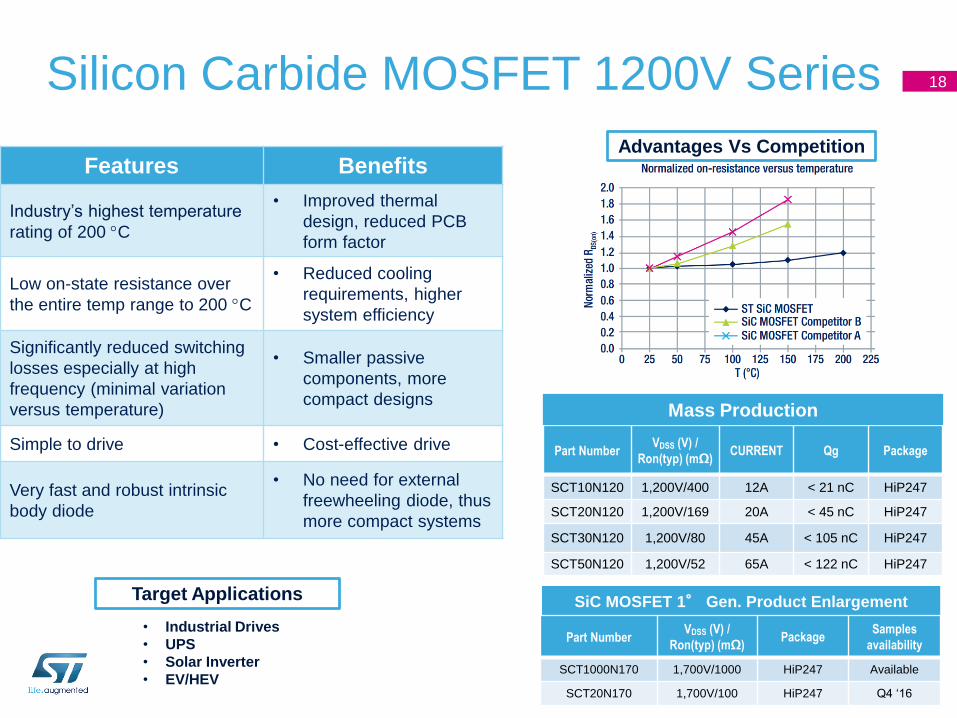
Features Benefits
Industry’s highest temperature
rating of 200 C
• Improved thermal
design, reduced PCB
form factor
Low on-state resistance over
the entire temp range to 200 C
• Reduced cooling
requirements, higher
system efficiency
Significantly reduced switching
losses especially at high
frequency (minimal variation
versus temperature)
• Smaller passive
components, more
compact designs
Simple to drive • Cost-effective drive
Very fast and robust intrinsic
body diode
• No need for external
freewheeling diode, thus
more compact systems
Advantages Vs Competition
Target Applications
• Industrial Drives
• UPS
• Solar Inverter
• EV/HEV
Part NumberVDSS (V) /
Ron(typ) (mΩ)CURRENT Qg Package
SCT10N120 1,200V/400 12A < 21 nC HiP247
SCT20N120 1,200V/169 20A < 45 nC HiP247
SCT30N120 1,200V/80 45A < 105 nC HiP247
SCT50N120 1,200V/52 65A < 122 nC HiP247
Mass Production
SiC MOSFET 1° Gen. Product Enlargement
Part NumberVDSS (V) /
Ron(typ) (mΩ)Package
Samples
availability
SCT1000N170 1,700V/1000 HiP247 Available
SCT20N170 1,700V/100 HiP247 Q4 ‘16
Silicon Carbide MOSFET 1200V Series 18

Efficiency vs frequency in a boost converter
Main Benefits
Impact on passive components:
Less volume
Lower losses on Magnetic
Lower weight
System Cost reduction
SiC MOSFET portfolio
Part Number
VDSS (V) /
Ron(typ)
(mΩ)
Package RemarkSamples
availability
SCTW100N65G2 650V/20 HiP247/ die sellBest Ron Option for
InverterQ4 2016
SCTW90N65G2V
SCTH9065G2V-7650V/25
HiP247
H2PAK-7L
rated 175°C
Low Qg Option for
Charger /
HF ConvertersAvailable
SCTH35N65G2V-7
SCTW35N65G2V650V/50
H2PAK-7 @ 175°C
HiP247 @ 200°C
Low Qg Option for
Charger / HF
ConvertersQ4 2016
• Rdson (@25°C) : 20 mΩ
• Rdson (@200°C) : 26 mΩMDmeshTM M6
MDmeshTM M5
SiC 650V
Main Competitor
Ron vs temperature
Silicon Carbide MOSFET
650V 2nd Gen. Series19

Power MOSFETPackage

(*) Long Lead Version Available
TO247-4
TO-220
TO-220FP TO-3PF
TO-3P
TO-247(*)
MAX247(*)
IPAK
Through Packages Overview for MOSFETs
21
Efficiency comparison
MOSFET portfolio
TO247-4Leads
BVDSS
[V]
RDSon
[mΩ]
ID
[A]P/N Main application
Eng.
Samples
600
40 68 STW70N60M2-4
PV-Inverter,
Server, UPSavailable
55 50 STW56N60M2-4
70 40 STW48N60M2-4
88 34 STW40N60M2-4
650 62 110 STW56N65M2-4Servers, SMPS,
Solaravailable
650
29 84 STW88N65M5-4
PV-Inverter,
Server, UPS available
45 58 STW69N65M5-4
63 42 STW57N65M5-4
98 30 STW38N65M5-4
4L PIN3L PIN
Temperature
Efficiency
∆η=0.34%
Key Features and Benefits
TO247-4 Features:
Kelvin Source PIN to separate power path from
driving signal
Increased creepage between PINs
TO247-4 Benefits:
Lower losses at both turn-off and turn-on
Higher efficiency
Lower working temperature Higher insulation standards
TO247-4 Package 22
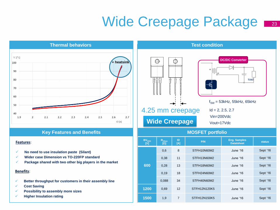
Thermal behaviors Test condition
DC/DC Converter
load
Id = 2, 2.5, 2.7
A
fSW = 53kHz, 55kHz, 65kHz
Vin=200Vdc
Vout=17VdcWide Creepage
Key Features and Benefits
+ heatsink
Features:
No need to use insulation paste (Silant)
Wider case Dimension vs TO-220FP standard
Package shared with two other big players in the market
Benefits:
Better throughput for customers in their assembly line
Cost Saving
Possibility to assembly more sizes
Higher Insulation rating
MOSFET portfolio
BVDSS
[V]
RDSon
[Ω]
ID
[A]P/N
Eng. Samples
Datatsheetstatus
600
0,6 8 STFH10N60M2 June ‘16 Sept ‘16
0,38 11 STFH13N60M2 June ‘16 Sept ‘16
0,28 13 STFH18N60M2 June ‘16 Sept ‘16
0,19 18 STFH24N60M2 June ‘16 Sept ‘16
0,088 34 STFH40N60M2 June ‘16 Sept ‘16
1200 0,69 12 STFH12N120K5 June ‘16 Sept ‘16
1500 1,9 7 STFH12N150K5 June ‘16 Sept ‘16
4.25 mm creepage
Wide Creepage Package 23

ST Rectifiers Product Range
B
R
I
D
G
E
S
24

600V/ 650V/ 1200V Diodes Series
and applications
Turn off
conditions
Low dIF/dt
turn off
Application
Discontinuous mode PFC
Secondary rectif
Resonant circuit
(Induction cooking)
Secondary side LLC converter
Technology 600V L series (STTHxL06)600V blank or AC Series
(STTHx06, STTHxAC06)
Hard
switching
Conditions
High dIF/dt
turn off
ApplicationMotor
control
Low Freq PFC, HVAC,
UPS, High freq drive
Hard switching PFC
Secondary rectification
In phase shift converter
High voltage output
Technology
650V/1200V Soft series
(JTHxMC065,
JTHxMC/HC12)
600V blank or AC Series,
1200V Soft,
blank or S Series
(STTHx12,STTHxS12)
600V R series (STTHxR06)
Tandem series (STTHxT06)
600V/650V/1200V SiC series
(STPSCxx)
0 60 10020
Low frequency Medium frequency Higher frequency
25

SiC Performances vs Si Techno
With SiC, we get :
- Best switching performances (fast and soft)
- Best efficiency in hard-switching applications thanks to best turn-off performance
Recovery current dependent on
Tj, IF and dI/dt
IF=8A ; dI/dt=400A/µs ; VR=400V ; Tj=125°C
2A/div ; 10ns/div
SiC 600/650V diode
Tandem G2
Capacitive current
independent of Tj
Tandem G1
Ultrafast diode
Reverse characteristics Power losses
26

Main Topologies Using 600/650V SiC Diodes
600V/650V SiC
single diode
ACAC
650V dual-diodes with
common cathode: save
one package and get
more integration
2 x 650V SiC diodes,
dual-diodes in series:
with high surge
capability
AC
Three SiC configurations available to cover a wide range of topologies
Single Boost PFC Interleaved PFC Bridgeless PFC
27

ST Products and RoadmapTO-247
or DO-247
TO-220AC TO-220AB
dual diodes
common cathode
TO-220AC insulated TO-220AB insulated
dual diodes
in series
D²PAK DPAK
600 V G1
4 A STPSC406D STPSC406B-TR
6 A STPSC606D STPSC606G-TR
8 A STPSC806D STPSC806G-TR
10 A STPSC1006D STPSC1006G-TR
12 A STPSC1206D
2 x 10 A STPSC2006CW
650 V G2
4 A STPSC4H065D STPSC4H065DI STPSC4H065B-TR
6 A STPSC6H065D STPSC6H065DI STPSC6H065G-TR STPSC6H065B-TR
8 A STPSC8H065D STPSC8H065DI STPSC8H065G-TR STPSC8H065B-TR
10 A
12A
STPSC10H065D
STPSC12H065D
STPSC10H065DI STPSC10H065G-TR STPSC10H065B-TR
2 x 4 A STPSC8H065CT
2 x 6 A STPSC12H065CT
2 x 8 A STPSC16H065CT
2 x 10 A STPSC20H065CW STPSC20H065CT
2 x 650 V G2
6 A STPSC6TH13TI
8A STPSC8TH13TI
10 A STPSC10TH13TI
1200 V
6 A STPSC6H12B-TR1
10 A STPSC10H12D
15 A
20A
STPSC15H12D
STPSC20H12D
28

FERD Diodes

Introduction to FERD Technology
• New rectifier family based on
patented ST technology
• Provide the best in class
VF/IR trade-off not achievable
with standard Power Schottky
technology
Positioning Vs Power
Schottky
SchottkyIR
VF
Same barrier
Different die-sizes
Different barrier
Same die-size
Barrier 1
Barrier 2Barrier 3
Die-size 2
>
Die-size 1
Same die size
Continuously tunable trade-off
IR
VF
Die-size 1
Anode
Cathode
N+
N-
30

• At light load: strong efficiency improvement
• At full load: strong thermal performance improvement & efficiency improvement
• Lower dependency of IRmax versus Tj & Lower leakage current ratio typ/max
=> To get more controlled design & more secure design
FERD 45V:Forward Voltage Characteristic
FERD30M45C vs. STPS3045C31
(AN4021: Calculation of reverse losses in a power diode)
FERD
STPS
[100°c-150°c]
C coeff0.04°C-1
[100°c-150°c]
C coeff0.06°C-1
thermal coefficient “c”

125c
75c
25c
150c
FERD30SM100STPS30M100
FERD30SM100
STPS30M10025c125c
Vplateau = 70 V
Vplateau2 = 20 V
tOFF1 = 2.5 µs
tOFF2 = 5 µs
tON = 7.2 µs
IMax = 10A
Application conditions
Vin = 264V(RMS), Tamb = 40°C,
Vout = 19V, Pout = 45W
FERD30SM100
STPS30M100
STPS41H100C
𝑷(𝑻𝒋) = 𝑷𝒄𝒐𝒏𝒅 𝑻𝒋 + 𝑷𝒓𝒆𝒗(𝑻𝒋)
FERD 100V: 45W Flyback Converter 32

100V FERD vs STPSxxH/S100 qualitative forward characteristics benchmark
33
VF
IF
FERD device STPS device IF approximate
crossing point at
125°C
FERD20S100STG STPS20S100CT ~5A
FERD20H100STG STPS20H100CT ~5A
FERD30H100STG STPS30H100CT ~8A
FERD40H100STG STPS41H100CT ~12AFERDxxH100 STPSxxH100
Vto1Vto2
rd1 rd2
<
>
Flyback working area
Crossing point
FERD & STPS have different characteristics shape,
with different Vto / rd values, linked to different technology

Adaptor 40WComparison FERD vs Schottky
34
FERD Benefits :
- Gain on VF (-50mV)
- Gain on efficiency (+0.3%)
FERDxxH100 is the replacement of STPSxxH100 Schottky
with better price and yield in adapter application

Differentiation Through InnovationFlat / package size reduction

ST Strategy 36
PowerFlat 5x6
SOD128F
2A to 8A SOD123F
SOD323F
< 1A
PSMC
TO-277A
Best in class VF / IR wiith FERD, enables to increase diodes current ratings
Packages downsizing to improve price/performances ratio& PCB cost
Deploy STPS/STTH/FERD available technologies in these packages
5A to 20A
* In development
1 to 3A
20A & more
STPS / FERD

8FL
4.7
2.4
0.98 0.98
3.50
7.95
5.90
2.30
5.35
3.62
5.07
2.57
2.30
(SMAFlat)
(SlimSMA)
(M-Flat)
(S-Flat)
(PMDU)
(G1F)
SODxxx Flat vs Other Packages 37

Key Takeaways
• STMicroelectronics is one of the world's leading suppliers of power
discrete semiconductor devices.
• ST provides the whole set of power devices:
MOSFET, SiC MOSFET, silicon rectifier, SiC diode, IGBT
• ST solution covers the requirements of many power management
applications. It improves the system efficiency, increases power-
density and brings lower-standby power design solutions.
• ST provides the best, complete and optimized power management
solution. It helps end customer to reduce the investigation cost and
reduces the time to market.
38

Thank you!