distributed by: 1-800-831-4242 … communication on multipoint bus-transmissionlines. the drivers...
TRANSCRIPT

The content and copyrights of the attached material are the property of its owner.
Distributed by:
www.Jameco.com 1-800-831-4242
www.ti.com
FEATURES DESCRIPTION
APPLICATIONS
1
2
3
4
8
7
6
5
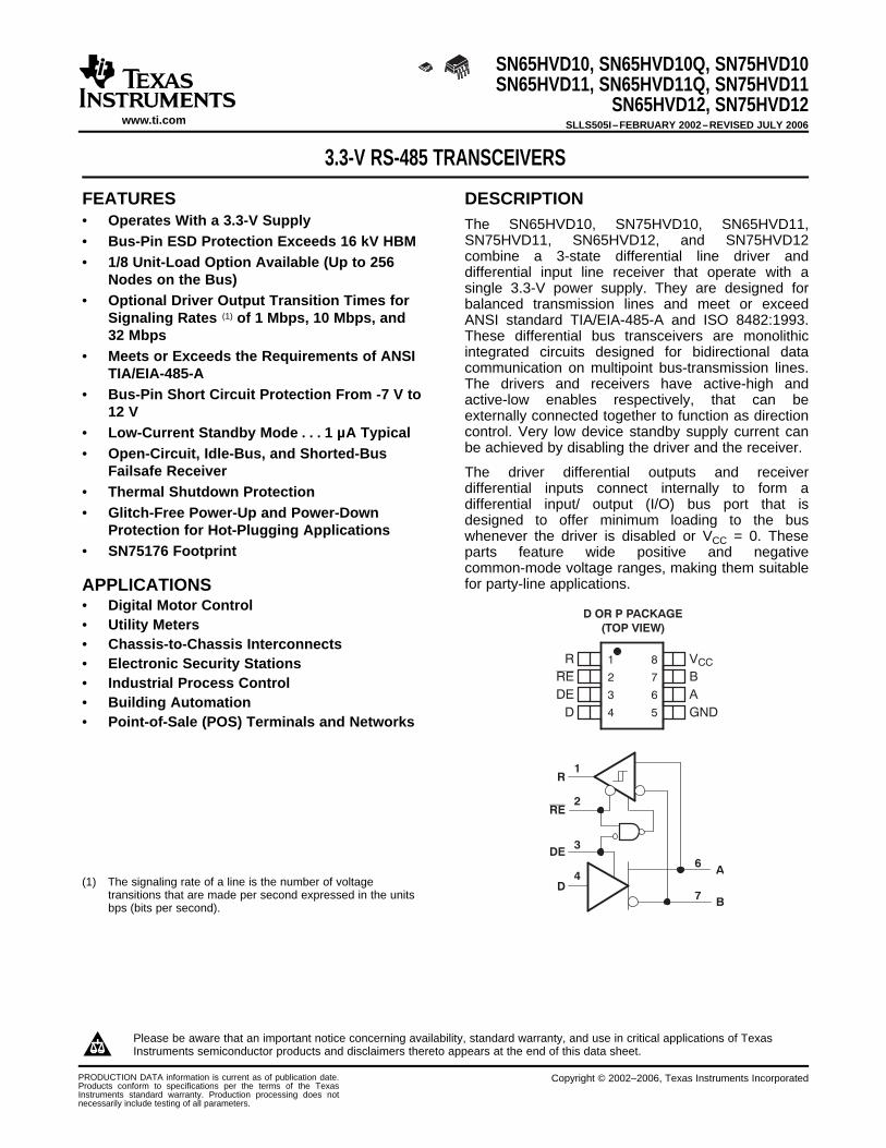
R
RE
DE
D
VCC
B
A
GND
D OR P PACKAGE
(TOP VIEW)
1
2
3
4
6
7
A
B
R
RE
DE
D
SN65HVD10, SN65HVD10Q, SN75HVD10SN65HVD11, SN65HVD11Q, SN75HVD11
SN65HVD12, SN75HVD12SLLS505I–FEBRUARY 2002–REVISED JULY 2006
3.3-V RS-485 TRANSCEIVERS
• Operates With a 3.3-V Supply The SN65HVD10, SN75HVD10, SN65HVD11,SN75HVD11, SN65HVD12, and SN75HVD12• Bus-Pin ESD Protection Exceeds 16 kV HBMcombine a 3-state differential line driver and• 1/8 Unit-Load Option Available (Up to 256differential input line receiver that operate with aNodes on the Bus)single 3.3-V power supply. They are designed for
• Optional Driver Output Transition Times for balanced transmission lines and meet or exceedSignaling Rates (1) of 1 Mbps, 10 Mbps, and ANSI standard TIA/EIA-485-A and ISO 8482:1993.32 Mbps These differential bus transceivers are monolithic
integrated circuits designed for bidirectional data• Meets or Exceeds the Requirements of ANSIcommunication on multipoint bus-transmission lines.TIA/EIA-485-AThe drivers and receivers have active-high and
• Bus-Pin Short Circuit Protection From -7 V to active-low enables respectively, that can be12 V externally connected together to function as direction
control. Very low device standby supply current can• Low-Current Standby Mode . . . 1 µA Typicalbe achieved by disabling the driver and the receiver.• Open-Circuit, Idle-Bus, and Shorted-Bus
Failsafe Receiver The driver differential outputs and receiverdifferential inputs connect internally to form a• Thermal Shutdown Protectiondifferential input/ output (I/O) bus port that is• Glitch-Free Power-Up and Power-Down designed to offer minimum loading to the bus
Protection for Hot-Plugging Applications whenever the driver is disabled or VCC = 0. These• SN75176 Footprint parts feature wide positive and negative
common-mode voltage ranges, making them suitablefor party-line applications.
• Digital Motor Control• Utility Meters• Chassis-to-Chassis Interconnects• Electronic Security Stations• Industrial Process Control• Building Automation• Point-of-Sale (POS) Terminals and Networks
(1) The signaling rate of a line is the number of voltagetransitions that are made per second expressed in the unitsbps (bits per second).
Please be aware that an important notice concerning availability, standard warranty, and use in critical applications of TexasInstruments semiconductor products and disclaimers thereto appears at the end of this data sheet.
PRODUCTION DATA information is current as of publication date. Copyright © 2002–2006, Texas Instruments IncorporatedProducts conform to specifications per the terms of the TexasInstruments standard warranty. Production processing does notnecessarily include testing of all parameters.

www.ti.com
ABSOLUTE MAXIMUM RATINGS
PACKAGE DISSIPATION RATINGS
SN65HVD10, SN65HVD10Q, SN75HVD10SN65HVD11, SN65HVD11Q, SN75HVD11SN65HVD12, SN75HVD12SLLS505I–FEBRUARY 2002–REVISED JULY 2006
These devices have limited built-in ESD protection. The leads should be shorted together or the device placed in conductive foamduring storage or handling to prevent electrostatic damage to the MOS gates.
ORDERING INFORMATION
PACKAGESIGNALING UNIT LOADS TA SOIC MARKINGRATE SOIC (1) PDIP
32 Mbps 1/2 SN65HVD10D SN65HVD10P VP10
10 Mbps 1/8 -40°C to 85°C SN65HVD11D SN65HVD11P VP11
1 Mbps 1/8 SN65HVD12D SN65HVD12P VP12
32 Mbps 1/2 SN75HVD10D SN75HVD10P VN10
10 Mbps 1/8 -0°C to 70°C SN75HVD11D SN75HVD11P VN11
1 Mbps 1/8 SN75HVD12D SN75HVD12P VN12
32 Mbps 1/2 SN65HVD10QD SN65HVD10QP VP10Q-40°C to 125°C
10 Mbps 1/8 SN65HVD11QD SN65HVD11QP VP11Q
(1) The D package is available taped and reeled. Add an R suffix to the part number (i.e., SN75HVD11DR).
over operating free-air temperature range unless otherwise noted (1) (2)
SN65HVD10, SN75HVD10,SN65HVD11, SN75HVD11,SN65HVD12, SN75HVD12
UNIT
VCC Supply voltage range -0.3 V to 6 V
Voltage range at A or B -9 V to 14 V
Input voltage range at D, DE, R or RE -0.5 V to VCC + 0.5 V
Voltage input range, transient pulse, A and B, through 100 Ω, see Figure 11 -50 V to 50 V
IO Receiver output current -11 mA to 11 mA
A, B, and GND 16 kVHuman body model (3)
Electrostatic discharge All pins 4 kV
Charged-device model (4) All pins charge 1 kV
Continuous total power dissipation See Dissipation Rating Table
TJ Junction temperature 170°
(1) Stresses beyond those listed under absolute maximum ratings may cause permanent damage to the device. These are stress ratingsonly, and functional operation of the device at these or any other conditions beyond those indicated under recommended operatingconditions is not implied. Exposure to absolute-maximum-rated conditions for extended periods may affect device reliability.
(2) All voltage values, except differential I/O bus voltages, are with respect to network ground terminal.(3) Tested in accordance with JEDEC Standard 22, Test Method A114-A.(4) Tested in accordance with JEDEC Standard 22, Test Method C101.
PACKAGE TA ≤ 25°C DERATING FACTOR (1) TA = 70°C TA = 85°C TA = 125°CPOWER RATING ABOVE TA = 25°C POWER RATING POWER RATING POWER RATING
D (2) 597 mW 4.97 mW/°C 373 mW 298 mW 100 mW
D (3) 990 mW 8.26 mW/°C 620 mW 496 mW 165 mW
P 1290 mW 10.75 mW/°C 806 mW 645 mW 215 mW
(1) This is the inverse of the junction-to-ambient thermal resistance when board-mounted and with no air flow.(2) Tested in accordance with the Low-K thermal metric definitions of EIA/JESD51-3.(3) Tested in accordance with the High-K thermal metric definitions of EIA/JESD51-7.
2 Submit Documentation Feedback

www.ti.com
RECOMMENDED OPERATING CONDITIONS
DRIVER ELECTRICAL CHARACTERISTICS
SN65HVD10, SN65HVD10Q, SN75HVD10SN65HVD11, SN65HVD11Q, SN75HVD11
SN65HVD12, SN75HVD12SLLS505I–FEBRUARY 2002–REVISED JULY 2006
over operating free-air temperature range unless otherwise noted
MIN NOM MAX UNIT
VCC Supply voltage 3 3.6
VI or VIC Voltage at any bus terminal (separately or common mode) -7 (1) 12
VIH High-level input voltage D, DE, RE 2 VCC V
VIL Low-level input voltage D, DE, RE 0 0.8
VID Differential input voltage Figure 7 -12 12
Driver -60IOH High-level output current mA
Receiver -8
Driver 60IOL Low-level output current mA
Receiver 8
RL Differential load resistance 54 60 Ω
CL Differential load capacitance 50 pF
HVD10 32
Signaling rate HVD11 10 Mbps
HVD12 1
TJ(2) Junction temperature 145 °C
(1) The algebraic convention, in which the least positive (most negative) limit is designated as minimum is used in this data sheet.(2) See thermal characteristics table for information regarding this specification.
over recommended operating conditions unless otherwise noted
PARAMETER TEST CONDITIONS MIN TYP (1) MAX UNIT
VIK Input clamp voltage II = -18 mA -1.5 V
IO = 0 2 VCC
|VOD| Differential output voltage (2) RL = 54 Ω, See Figure 1 1.5 V
Vtest = -7 V to 12 V, See Figure 2 1.5
Change in magnitude of differential output∆|VOD| See Figure 1 and Figure 2 -0.2 0.2 Vvoltage
VOC(PP) Peak-to-peak common-mode output voltage 400 mV
VOC(SS) Steady-state common-mode output voltage 1.4 2.5 VSee Figure 3Change in steady-state common-mode output∆VOC(SS) -0.05 0.05 Vvoltage
IOZ High-impedance output current See receiver input currents
D -100 0II Input current µA
DE 0 100
IOS Short-circuit output current -7 V ≤ VO ≤ 12 V -250 250 mA
C(OD) Differential output capacitance VOD = 0.4 sin (4E6πt) + 0.5 V, DE at 0 V 16 pF
RE at VCC, Receiver disabled andD & DE at VCC, 9 15.5 mAdriver enabledNo load
RE at VCC,D at VCC, Receiver disabled andICC Supply current 1 5 µADE at 0 V, driver disabled (standby)No load
RE at 0 V, Receiver enabled andD & DE at VCC, 9 15.5 mAdriver enabledNo load
(1) All typical values are at 25°C and with a 3.3-V supply.(2) For TA > 85°C, VCC is ±5%.
3Submit Documentation Feedback

www.ti.com
DRIVER SWITCHING CHARACTERISTICS
SN65HVD10, SN65HVD10Q, SN75HVD10SN65HVD11, SN65HVD11Q, SN75HVD11SN65HVD12, SN75HVD12SLLS505I–FEBRUARY 2002–REVISED JULY 2006
over recommended operating conditions unless otherwise noted
PARAMETER TEST CONDITIONS MIN TYP (1) MAX UNIT
HVD10 5 8.5 16
tPLH Propagation delay time, low-to-high-level output HVD11 18 25 40 ns
HVD12 135 200 300
HVD10 5 8.5 16
tPHL Propagation delay time, high-to-low-level output HVD11 18 25 40 ns
HVD12 135 200 300
HVD10 3 4.5 10RL = 54 Ω, CL = 50 pF,tr Differential output signal rise time HVD11 10 20 30 nsSee Figure 4
HVD12 100 170 300
HVD10 3 4.5 10
tf Differential output signal fall time HVD11 10 20 30 ns
HVD12 100 170 300
HVD10 1.5
tsk(p) Pulse skew (|tPHL - tPLH|) HVD11 2.5 ns
HVD12 7
HVD10 6
tsk(pp)(2) Part-to-part skew HVD11 11 ns
HVD12 100
HVD10 31Propagation delay time,tPZH HVD11 55 nshigh-impedance-to-high-level output
HVD12 300RL = 110 Ω, RE at 0 V,See Figure 5HVD10 25
Propagation delay time,tPHZ HVD11 55 nshigh-level-to-high-impedance outputHVD12 300
HVD10 26Propagation delay time,tPZL HVD11 55 nshigh-impedance-to-low-level output
HVD12 300RL = 110 Ω, RE at 0 V,See Figure 6HVD10 26
Propagation delay time,tPLZ HVD11 75 nslow-level-to-high-impedance outputHVD12 400
RL = 110 Ω, RE at 3 V,tPZH Propagation delay time, standby-to-high-level output 6 µsSee Figure 5
RL = 110 Ω, RE at 3 V,tPZL Propagation delay time, standby-to-low-level output 6 µsSee Figure 6
(1) All typical values are at 25°C and with a 3.3-V supply.(2) tsk(pp) is the magnitude of the difference in propagation delay times between any specified terminals of two devices when both devices
operate with the same supply voltages, at the same temperature, and have identical packages and test circuits.
4 Submit Documentation Feedback

www.ti.com
RECEIVER ELECTRICAL CHARACTERISTICS
SN65HVD10, SN65HVD10Q, SN75HVD10SN65HVD11, SN65HVD11Q, SN75HVD11
SN65HVD12, SN75HVD12SLLS505I–FEBRUARY 2002–REVISED JULY 2006
over recommended operating conditions unless otherwise noted
PARAMETER TEST CONDITIONS MIN TYP (1) MAX UNIT
Positive-going input thresholdVIT+ IO = -8 mA -0.01voltageV
Negative-going input thresholdVIT- IO = 8 mA -0.2voltage
Vhys Hysteresis voltage (VIT+ - VIT-) 35 mV
VIK Enable-input clamp voltage II = -18 mA -1.5 V
VOH High-level output voltage VID = 200 mV, IOH = -8 mA, See Figure 7 2.4 V
VOL Low-level output voltage VID = -200 mV, IOL = 8 mA, See Figure 7 0.4 V
IOZ High-impedance-state output current VO = 0 or VCC RE at VCC -1 1 µA
VA or VB = 12 V 0.05 0.11
VA or VB = 12 V, VCC = 0 V 0.06 0.13HVD11, HVD12, mAOther input at 0 VVA or VB = -7 V -0.1 -0.05
VA or VB = -7 V, VCC = 0 V -0.05 -0.04II Bus input current
VA or VB = 12 V 0.2 0.5
VA or VB = 12 V, VCC = 0 V 0.25 0.5HVD10, mAOther input at 0 VVA or VB = -7 V -0.4 -0.2
VA or VB = -7 V, VCC = 0 V -0.4 -0.15
IIH High-level input current, RE VIH = 2 V -30 0 µA
IIL Low-level input current, RE VIL = 0.8 V -30 0 µA
CID Differential input capacitance VID = 0.4 sin (4E6πt) + 0.5 V, DE at 0 V 15 pF
RE at 0 V, Receiver enabled and driverD & DE at 0 V, 4 8 mAdisabledNo load
RE at VCC,D at VCC, Receiver disabled and driverICC Supply current 1 5 µADE at 0 V, disabled (standby)No load
RE at 0 V, Receiver enabled and driverD & DE at VCC, 9 15.5 mAenabledNo load
(1) All typical values are at 25°C and with a 3.3-V supply.
5Submit Documentation Feedback

www.ti.com
RECEIVER SWITCHING CHARACTERISTICS
THERMAL CHARACTERISTICS
SN65HVD10, SN65HVD10Q, SN75HVD10SN65HVD11, SN65HVD11Q, SN75HVD11SN65HVD12, SN75HVD12SLLS505I–FEBRUARY 2002–REVISED JULY 2006
over recommended operating conditions unless otherwise noted
PARAMETER TEST CONDITIONS MIN TYP (1) MAX UNIT
tPLH Propagation delay time, low-to-high-level output HVD10 12.5 20 25ns
tPHL Propagation delay time, high-to-low-level output HVD10 12.5 20 25
HVD11tPLH Propagation delay time, low-to-high-level output 30 55 70 nsHVD12 VID = -1.5 V to 1.5 V,HVD11 CL = 15 pF,tPHL Propagation delay time, high-to-low-level output 30 55 70 nsHVD12 See Figure 8
HVD10 1.5
tsk(p) Pulse skew (|tPHL - tPLH|) HVD11 4 ns
HVD12 4
HVD10 8
tsk(pp)(2) Part-to-part skew HVD11 15 ns
HVD12 15
tr Output signal rise time 1 2 5CL = 15 pF, nsSee Figure 8tf Output signal fall time 1 2 5
tPZH(1) Output enable time to high level 15
tPZL(1) Output enable time to low level 15CL = 15 pF, DE at 3 V, nsSee Figure 9tPHZ Output disable time from high level 20
tPLZ Output disable time from low level 15
tPZH(2) Propagation delay time, standby-to-high-level output 6CL = 15 pF, DE at 0, µsSee Figure 10tPZL(2) Propagation delay time, standby-to-low-level output 6
(1) All typical values are at 25°C and with a 3.3-V supply(2) tsk(pp) is the magnitude of the difference in propagation delay times between any specified terminals of two devices when both devices
operate with the same supply voltages, at the same temperature, and have identical packages and test circuits.
over operating free-air temperature range unless otherwise noted (1)
PARAMETER TEST CONDITIONS MIN TYP MAX UNIT
High–K board (3), No airflow D pkg 121Junction–to–ambient thermalθJA resistance (2) No airflow (4) P pkg 93
High–K board D pkg 67Junction–to–board thermalθJB °C/Wresistance See (4) P pkg 57
D pkg 41Junction–to–case thermalθJC resistance P pkg 55
HVD10 198 250(32 Mbps)RL= 60 Ω, CL = 50 pF,
DE at VCC, RE at 0 V, HVD11 141 176PD Device power dissipation mWInput to D a 50% duty cycle square (10 Mbps)wave at indicated signaling rate HVD12 133 161
(500 kbps)
High–K board, No airflow D pkg -40 116TA Ambient air temperature
No airflow (4) P pkg -40 123 °C
TJSD Thermal shutdown junction temperature 165
(1) See Application Information section for an explanation of these parameters.(2) The intent of θJA specification is solely for a thermal performance comparison of one package to another in a standardized environment.
This methodology is not meant to and will not predict the performance of a package in an application-specific environment.(3) JSD51–7, High Effective Thermal Conductivity Test Board for Leaded Surface Mount Packages.(4) JESD51–10, Test Boards for Through-Hole Perimeter Leaded Package Thermal Measurements.
6 Submit Documentation Feedback

www.ti.com
PARAMETER MEASUREMENT INFORMATION
60 Ω ±1%VOD0 or 3 V
_+
−7 V < V(test) < 12 V
DE
VCC
A
B
D
375 Ω ±1%
375 Ω ±1%
IOA
VOD 54 Ω ±1%0 or 3 V
VOAVOB
IOB
DE
VCC
II
VI
A
B
VOC
27 Ω ± 1%
Input
A
B
VA
VB
VOC(PP) ∆VOC(SS)
VOC
27 Ω ± 1%
CL = 50 pF ±20%
DA
B
DE
VCC
Input: PRR = 500 kHz, 50% Duty Cycle,tr<6ns, tf<6ns, ZO = 50 Ω
CL Includes Fixture andInstrumentation Capacitance
VOD
RL = 54 Ω± 1%50 Ω
Generator: PRR = 500 kHz, 50% Duty Cycle, tr <6 ns, tf <6 ns, Zo = 50 Ω
tPLH tPHL
1.5 V 1.5 V
3 V
≈ 2 V
≈ –2 V
90%
10%0 V
VI
VOD
tr tf
CL = 50 pF ±20%
CL Includes Fixtureand InstrumentationCapacitance
DA
B
DE
VCC
VIInput
Generator90%
0 V10%
RL = 110 Ω ± 1%Input
Generator 50 Ω
Generator: PRR = 500 kHz, 50% Duty Cycle, tr <6 ns, tf <6 ns, Zo = 50 Ω
3 VS1
0.5 V
3 V
0 V
VOH
≈ 0 VtPHZ
tPZH
1.5 V 1.5 VVI
VO
CL = 50 pF ±20%
CL Includes Fixtureand Instrumentation
Capacitance
DA
BDE
VO
VI
2.3 V
SN65HVD10, SN65HVD10Q, SN75HVD10SN65HVD11, SN65HVD11Q, SN75HVD11
SN65HVD12, SN75HVD12SLLS505I–FEBRUARY 2002–REVISED JULY 2006
Figure 1. Driver VOD Test Circuit and Voltage and Figure 2. Driver VOD With Common-Mode Loading TestCurrent Definitions Circuit
Figure 3. Test Circuit and Definitions for the Driver Common-Mode Output Voltage
Figure 4. Driver Switching Test Circuit and Voltage Waveforms
Figure 5. Driver High-Level Enable and Disable Time Test Circuit and Voltage Waveforms
7Submit Documentation Feedback
www.ti.com
InputGenerator 50 Ω
3 V VO
S1
3 V
1.5 V 1.5 V
tPZL tPLZ
2.3 V0.5 V
≈ 3 V
0 V
VOL
VI
VO
Generator: PRR = 500 kHz, 50% Duty Cycle, tr <6 ns, tf <6 ns, Zo = 50 Ω
RL = 110 Ω ± 1%
CL = 50 pF ±20%
CL Includes Fixtureand Instrumentation
Capacitance
DA
BDE
VI
≈ 3 V
VIDVA
VB
IOA
B
IB VO
R
IA
VICVA + VB
2
InputGenerator 50 Ω
Generator: PRR = 500 kHz, 50% Duty Cycle, tr <6 ns, tf <6 ns, Zo = 50 Ω
VO
1.5 V
0 V
1.5 V 1.5 V
3 V
VOH
VOL
1.5 V10%
1.5 V
tPLH tPHL
tr tf
90%
VI
VO
CL = 15 pF ±20%
CL Includes Fixtureand InstrumentationCapacitance
A
B
RE
VI
R
0 V
90%
10%
SN65HVD10, SN65HVD10Q, SN75HVD10SN65HVD11, SN65HVD11Q, SN75HVD11SN65HVD12, SN75HVD12SLLS505I–FEBRUARY 2002–REVISED JULY 2006
PARAMETER MEASUREMENT INFORMATION (continued)
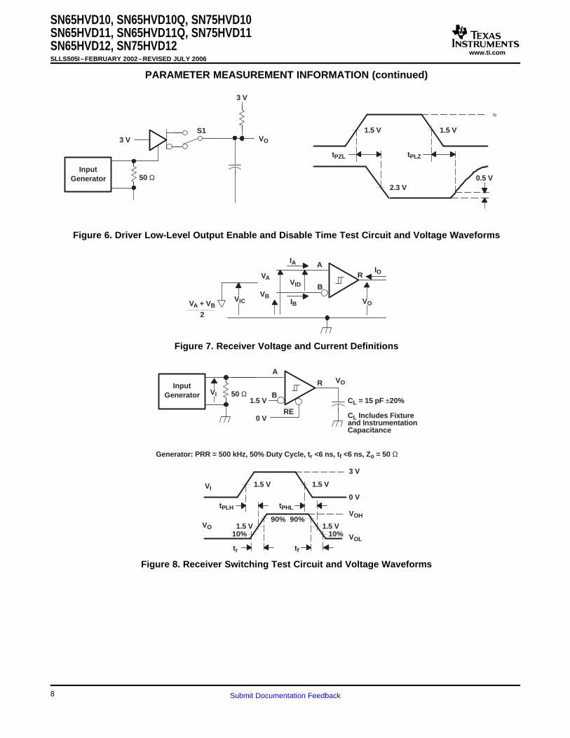
Figure 6. Driver Low-Level Output Enable and Disable Time Test Circuit and Voltage Waveforms
Figure 7. Receiver Voltage and Current Definitions
Figure 8. Receiver Switching Test Circuit and Voltage Waveforms
8 Submit Documentation Feedback
www.ti.com
50 Ω
Generator: PRR = 500 kHz, 50% Duty Cycle, tr <6 ns, tf <6 ns, Zo = 50 Ω
VO
RE
RA
B
3 V
0 V or 3 V
3 V
1.5 V 1.5 V
tPZH(1) tPHZ
1.5 VVOH –0.5 V
3 V
0 V
VOH
≈ 0 V
VO
CL = 15 pF ±20%
CL Includes Fixtureand InstrumentationCapacitance
VI
DED
1 kΩ ± 1%
VI
A
B
S1
D at 3 VS1 to B
tPZL(1) tPLZ
1.5 VVOL +0.5 V
≈ 3 V
VOL
VO
D at 0 VS1 to A
InputGenerator
SN65HVD10, SN65HVD10Q, SN75HVD10SN65HVD11, SN65HVD11Q, SN75HVD11
SN65HVD12, SN75HVD12SLLS505I–FEBRUARY 2002–REVISED JULY 2006
PARAMETER MEASUREMENT INFORMATION (continued)
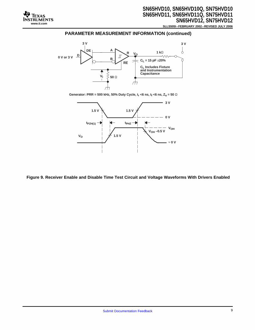
Figure 9. Receiver Enable and Disable Time Test Circuit and Voltage Waveforms With Drivers Enabled
9Submit Documentation Feedback
www.ti.com
InputGenerator 50 Ω
Generator: PRR = 100 kHz, 50% Duty Cycle, tr <6 ns, tf <6 ns, Zo = 50 Ω
VO
RE
RA
B
3 V
1.5 V
tPZH(2)
1.5 V
3 V
0 V
VOH
GND
VI
VO
0 V or 1.5 V
1.5 V or 0 V CL = 15 pF ±20%
CL Includes Fixtureand InstrumentationCapacitanceVI
1 kΩ ± 1%A
B
S1
A at 1.5 VB at 0 VS1 to B
tPZL(2)
1.5 V
3 V
VOL
VO
A at 0 VB at 1.5 VS1 to A
Pulse Generator,15 µs Duration,1% Duty Cycletr, tf ≤ 100 ns
100 Ω± 1%
_+
A
BR
D
DE
RE
0 V or 3 V
NOTE: This test is conducted to test survivability only. Data stability at the R output is not specified.
3 V or 0 V
SN65HVD10, SN65HVD10Q, SN75HVD10SN65HVD11, SN65HVD11Q, SN75HVD11SN65HVD12, SN75HVD12SLLS505I–FEBRUARY 2002–REVISED JULY 2006
PARAMETER MEASUREMENT INFORMATION (continued)
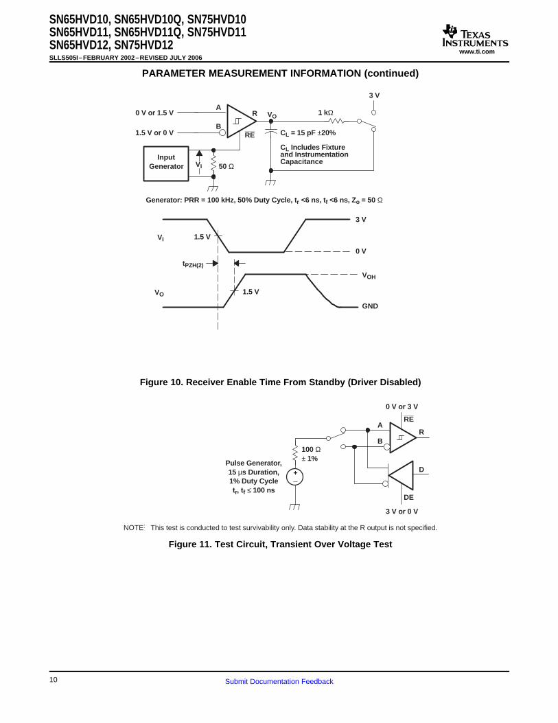
Figure 10. Receiver Enable Time From Standby (Driver Disabled)
Figure 11. Test Circuit, Transient Over Voltage Test
10 Submit Documentation Feedback

www.ti.com
FUNCTION TABLES
SN65HVD10, SN65HVD10Q, SN75HVD10SN65HVD11, SN65HVD11Q, SN75HVD11
SN65HVD12, SN75HVD12SLLS505I–FEBRUARY 2002–REVISED JULY 2006
PARAMETER MEASUREMENT INFORMATION (continued)
DRIVER (1)
OUTPUTS
INPUT ENABLE A BD DE
H H H L
L H L H
X L Z Z
Open H H L
(1) H = high levelL = low levelZ = high impedanceX = irrelevant? = indeterminate
RECEIVER (1)
DIFFERENTIAL INPUTS ENABLE OUTPUTVID = VA - VB RE R
VID ≤ –0.2 V L L
–0.2 V < VID < –0.01 V L ?
–0.01 V ≤ VID L H
X H Z
Open Circuit L H
Short circuit L H
(1) H = high levelL = low levelZ = high impedanceX = irrelevant? = indeterminate
11Submit Documentation Feedback
www.ti.com
EQUIVALENT INPUT AND OUTPUT SCHEMATIC DIAGRAMS
9 V
1 kΩ
100 kΩ
Input
VCC
D and RE Inputs
9 V
1 kΩ
100 kΩ
Input
VCC
DE Input
16 V
16 V
R3R1
R2
Input
A Input
16 V
16 V
R3R1
R2
Input
B Input
16 V
16 V
VCC
A and B Outputs
9 V
VCC
R Output
5 ΩOutput
VCC
SN65HVD10
SN65HVD11
SN65HVD12
R1/R2
9 kΩ36 kΩ36 kΩ
R3
45 kΩ180 kΩ180 kΩ
VCC
Output
SN65HVD10, SN65HVD10Q, SN75HVD10SN65HVD11, SN65HVD11Q, SN75HVD11SN65HVD12, SN75HVD12SLLS505I–FEBRUARY 2002–REVISED JULY 2006
12 Submit Documentation Feedback
www.ti.com
TYPICAL CHARACTERISTICS
30
40
50
60
70
0 2.5 5 7.5 10
VCC = 3.6 V
VCC = 3.3 V
VCC = 3 V
Signaling Rate − Mbps
I CC
− R
MS
Sup
ply
Cur
rent
− m
A
TA = 25°CRE at VCCDE at VCC
RL = 54 ΩCL = 50 pF
30
40
50
60
70
0 5 10 15 20 25 30 35 40
I CC
TA = 25°CRE at VCCDE at VCC
VCC = 3.6 V
VCC = 3.3 V
VCC = 3 V
− R
MS
Sup
ply
Cur
rent
− m
A
Signaling Rate − Mbps
RL = 54 ΩCL = 50 pF
30
40
50
60
70
100 400 700 1000
VCC = 3.6 V
VCC = 3.3 V
VCC = 3 V
Signaling Rate − kbps
I CC
− R
MS
Sup
ply
Cur
rent
− m
A
TA = 25°CRE at VCCDE at VCC
RL = 54 ΩCL = 50 pF
−200
−150
−100
−50
0
50
100
150
200
250
300
−7 −6−5 −4−3 −2−1 0 1 2 3 4 5 6 7 8 9 10 11 12
− B
us In
put C
urre
nt −
I IA
µ
VI − Bus Input V oltage − V
VCC = 0 V
VCC = 3.3 V
TA = 25°CDE at 0 V
SN65HVD10, SN65HVD10Q, SN75HVD10SN65HVD11, SN65HVD11Q, SN75HVD11
SN65HVD12, SN75HVD12SLLS505I–FEBRUARY 2002–REVISED JULY 2006
HVD10 HVD11RMS SUPPLY CURRENT RMS SUPPLY CURRENT
vs vsSIGNALING RATE SIGNALING RATE
Figure 12. Figure 13.
HVD12 HVD10RMS SUPPLY CURRENT BUS INPUT CURRENT
vs vsSIGNALING RATE BUS INPUT VOLTAGE
Figure 14. Figure 15.
13Submit Documentation Feedback

www.ti.com
−200
−150
−100
−50
0
50
100
150
−4 −2 0 2 4 6
TA = 25°CDE at VCCD at VCCVCC = 3.3 V
VOH − Driver High-Level Output V oltage − V
I OH
− H
igh-
Leve
l Out
put C
urre
nt −
mA
−60
−50
−40
−30
−20
−10
010
20
30
40
50
60
70
80
90
−7−6−5−4−3−2−1 0 1 2 3 4 5 6 7 8 9 10 11 12
− B
us In
put C
urre
nt −
I IA
µ
VI − Bus Input V oltage − V
VCC = 0 V
VCC = 3.3 V
TA = 25°CDE at 0 V
− D
river
Diff
eren
tial O
utpu
t − V
1.5
1.6
1.7
1.8
1.9
2.0
2.1
2.2
2.3
2.4
2.5
−40 −15 10 35 60 85
VO
D
TA − Free-Air T emperature − °C
VCC = 3.3 VDE at VCCD at VCC
−20
0
20
40
60
80
100
120
140
160
180
200
−4 −2 0 2 4 6 8
TA = 25°CDE at VCCD at 0 VVCC = 3.3 V
VOL − Driver Low-Level Output V oltage − V
I OL
− Lo
w-L
evel
Out
put C
urre
nt −
mA
SN65HVD10, SN65HVD10Q, SN75HVD10SN65HVD11, SN65HVD11Q, SN75HVD11SN65HVD12, SN75HVD12SLLS505I–FEBRUARY 2002–REVISED JULY 2006
TYPICAL CHARACTERISTICS (continued)
HVD11 OR HVD12BUS INPUT CURRENT HIGH-LEVEL OUTPUT CURRENT
vs vsBUS INPUT VOLTAGE DRIVER HIGH-LEVEL OUTPUT VOLTAGE
Figure 16. Figure 17.
LOW-LEVEL OUTPUT CURRENT DRIVER DIFFERENTIAL OUTPUTvs vs
DRIVER LOW-LEVEL OUTPUT VOLTAGE FREE-AIR TEMPERATURE
Figure 18. Figure 19.
14 Submit Documentation Feedback

www.ti.com
VCC − Supply V oltage − V
−35
−30
−25
−20
−40
−15
−10
−5
− D
river
Out
put C
urre
nt −
mA
I O
00 0.50 1 1.50 2 2.50 3 3.50
TA = 25°CDE at VCCD at VCCRL = 54 Ω
HVD12
HVD11
0
100
400
500
600
-7 -2 3 8 13
HVD10
En
ab
le T
ime
−n
s
V −(TEST) Common-Mode Voltage − V
200
300
60 W
1%±
50 W
375 W 1%±
-7 V < V < 12 V(TEST)
VOD
V (low)OD
t (diff)pZL
t (diff)pZH
V
0 or 3 V
375 W 1%±
50%
0 V
1.5 V
D
Z
DE
Y
-1.5 V
V (high)OD
Input
Generator
SN65HVD10, SN65HVD10Q, SN75HVD10SN65HVD11, SN65HVD11Q, SN75HVD11
SN65HVD12, SN75HVD12SLLS505I–FEBRUARY 2002–REVISED JULY 2006
TYPICAL CHARACTERISTICS (continued)
DRIVER OUTPUT CURRENT ENABLE TIMEvs vs
SUPPLY VOLTAGE COMMON-MODE VOLTAGE (SEE Figure 22)
Figure 20. Figure 21.
Figure 22. Driver Enable Time From DE to VOD
The time tpZL(x) is the measure from DE to VOD(x). VOD is valid when it is greater than 1.5 V.
15Submit Documentation Feedback

www.ti.com
APPLICATION INFORMATION
RT RT
DeviceHVD10HVD11HVD12
Number of Devices on Bus64256256
NOTE: The line should be terminated at both ends with its characteristic impedance (RT = ZO). Stub lengths off the main lineshould be kept as short as possible.
Stub
Driver Input
Driver Output
Receiver Input
Receiver Output
SN65HVD10, SN65HVD10Q, SN75HVD10SN65HVD11, SN65HVD11Q, SN75HVD11SN65HVD12, SN75HVD12SLLS505I–FEBRUARY 2002–REVISED JULY 2006
Figure 23. Typical Application Circuit
Figure 24. HVD12 Input and Output Through 2000 Feet of Cable
length of Commscope 5524 category 5e+ twistedAn example application for the HVD12 is illustrated pair cable. The bus is terminated at each end by ain Figure 23. Two HVD12 transceivers are used to 100-Ω resistor, matching the cable characteristiccommunicate data through a 2000 foot (600 m) impedance. Figure 24 illustrates operation at a
signaling rate of 250 kbps.
16 Submit Documentation Feedback

www.ti.com
THERMAL CHARACTERISTICS OF IC
SN65HVD10, SN65HVD10Q, SN75HVD10SN65HVD11, SN65HVD11Q, SN75HVD11
SN65HVD12, SN75HVD12SLLS505I–FEBRUARY 2002–REVISED JULY 2006
θJC (Junction-to-Case Thermal Resistance) isPACKAGES defined as difference in junction temperature to case
divided by the operating power. It is measured byθJA (Junction-to-Ambient Thermal Resistance) is putting the mounted package up against a copperdefined as the difference in junction temperature to block cold plate to force heat to flow from die,ambient temperature divided by the operating power. through the mold compound into the copper block.θJA is not a constant and is a strong function of: θJC is a useful thermal characteristic when a heatsink• the PCB design (50% variation) is applied to package. It is not a useful characteristic• altitude (20% variation) to predict junction temperature because it provides
pessimistic numbers if the case temperature is• device power (5% variation)measured in a nonstandard system and junction
θJA can be used to compare the thermal performance temperatures are backed out. It can be used with θJBof packages if the specific test conditions are defined in 1-dimensional thermal simulation of a packageand used. Standardized testing includes specification system.of PCB construction, test chamber volume, sensor
θJB (Junction-to-Board Thermal Resistance) islocations, and the thermal characteristics of holdingdefined as the difference in the junction temperaturefixtures. θJA is often misused when it is used toand the PCB temperature at the center of thecalculate junction temperatures for other installations.package (closest to the die) when the PCB is
TI uses two test PCBs as defined by JEDEC clamped in a cold-plate structure. θJB is only definedspecifications. The low-k board gives average in-use for the high-k test card.condition thermal performance, and it consists of a
θJB provides an overall thermal resistance betweensingle copper trace layer 25 mm long and 2-oz thick.the die and the PCB. It includes a bit of the PCBThe high-k board gives best case in-use condition,thermal resistance (especially for BGA’s with thermaland it consists of two 1-oz buried power planes withballs) and can be used for simple 1-dimensionala single copper trace layer 25 mm long and 2-oznetwork analysis of package system, see Figure 25.thick. A 4% to 50% difference in θJA can be
measured between these two test cards.
Figure 25. Thermal Resistance
17Submit Documentation Feedback

PACKAGING INFORMATION
Orderable Device Status (1) PackageType
PackageDrawing
Pins PackageQty
Eco Plan (2) Lead/Ball Finish MSL Peak Temp (3)
SN65HVD10D ACTIVE SOIC D 8 75 Green (RoHS &no Sb/Br)
CU NIPDAU Level-1-260C-UNLIM
SN65HVD10DG4 ACTIVE SOIC D 8 75 Green (RoHS &no Sb/Br)
CU NIPDAU Level-1-260C-UNLIM
SN65HVD10DR ACTIVE SOIC D 8 1 Green (RoHS &no Sb/Br)
CU NIPDAU Level-1-260C-UNLIM
SN65HVD10DRG4 ACTIVE SOIC D 8 1 Green (RoHS &no Sb/Br)
CU NIPDAU Level-1-260C-UNLIM
SN65HVD10P ACTIVE PDIP P 8 50 Pb-Free(RoHS)
CU NIPDAU N / A for Pkg Type
SN65HVD10PE4 ACTIVE PDIP P 8 50 Pb-Free(RoHS)
CU NIPDAU N / A for Pkg Type
SN65HVD10QD ACTIVE SOIC D 8 75 Green (RoHS &no Sb/Br)
CU NIPDAU Level-1-260C-UNLIM
SN65HVD10QDG4 ACTIVE SOIC D 8 75 Green (RoHS &no Sb/Br)
CU NIPDAU Level-1-260C-UNLIM
SN65HVD10QDR ACTIVE SOIC D 8 2500 Green (RoHS &no Sb/Br)
CU NIPDAU Level-1-260C-UNLIM
SN65HVD10QDRG4 ACTIVE SOIC D 8 2500 Green (RoHS &no Sb/Br)
CU NIPDAU Level-1-260C-UNLIM
SN65HVD10QP ACTIVE PDIP P 8 50 Pb-Free(RoHS)
CU NIPDAU N / A for Pkg Type
SN65HVD10QPE4 ACTIVE PDIP P 8 50 Pb-Free(RoHS)
CU NIPDAU N / A for Pkg Type
SN65HVD11D ACTIVE SOIC D 8 75 Green (RoHS &no Sb/Br)
CU NIPDAU Level-1-260C-UNLIM
SN65HVD11DG4 ACTIVE SOIC D 8 75 Green (RoHS &no Sb/Br)
CU NIPDAU Level-1-260C-UNLIM
SN65HVD11DR ACTIVE SOIC D 8 2500 Green (RoHS &no Sb/Br)
CU NIPDAU Level-1-260C-UNLIM
SN65HVD11DRG4 ACTIVE SOIC D 8 2500 Green (RoHS &no Sb/Br)
CU NIPDAU Level-1-260C-UNLIM
SN65HVD11P ACTIVE PDIP P 8 50 Pb-Free(RoHS)
CU NIPDAU N / A for Pkg Type
SN65HVD11PE4 ACTIVE PDIP P 8 50 Pb-Free(RoHS)
CU NIPDAU N / A for Pkg Type
SN65HVD11QD ACTIVE SOIC D 8 75 TBD CU NIPDAU Level-1-220C-UNLIM
SN65HVD11QDR ACTIVE SOIC D 8 2500 TBD CU NIPDAU Level-1-220C-UNLIM
SN65HVD11QDRG4 ACTIVE SOIC D 8 TBD Call TI Call TI
SN65HVD11QP ACTIVE PDIP P 8 50 Pb-Free(RoHS)
CU NIPDAU N / A for Pkg Type
SN65HVD11QPE4 ACTIVE PDIP P 8 50 Pb-Free(RoHS)
CU NIPDAU N / A for Pkg Type
SN65HVD12D ACTIVE SOIC D 8 75 Green (RoHS &no Sb/Br)
CU NIPDAU Level-1-260C-UNLIM
SN65HVD12DG4 ACTIVE SOIC D 8 75 Green (RoHS &no Sb/Br)
CU NIPDAU Level-1-260C-UNLIM
SN65HVD12DR ACTIVE SOIC D 8 2500 Green (RoHS &no Sb/Br)
CU NIPDAU Level-1-260C-UNLIM
PACKAGE OPTION ADDENDUM
www.ti.com 2-Oct-2006
Addendum-Page 1

Orderable Device Status (1) PackageType
PackageDrawing
Pins PackageQty
Eco Plan (2) Lead/Ball Finish MSL Peak Temp (3)
SN65HVD12DRG4 ACTIVE SOIC D 8 2500 Green (RoHS &no Sb/Br)
CU NIPDAU Level-1-260C-UNLIM
SN65HVD12P ACTIVE PDIP P 8 50 Pb-Free(RoHS)
CU NIPDAU N / A for Pkg Type
SN65HVD12PE4 ACTIVE PDIP P 8 50 Pb-Free(RoHS)
CU NIPDAU N / A for Pkg Type
SN75HVD10D ACTIVE SOIC D 8 75 Green (RoHS &no Sb/Br)
CU NIPDAU Level-1-260C-UNLIM
SN75HVD10DG4 ACTIVE SOIC D 8 75 Green (RoHS &no Sb/Br)
CU NIPDAU Level-1-260C-UNLIM
SN75HVD10DR ACTIVE SOIC D 8 2500 Green (RoHS &no Sb/Br)
CU NIPDAU Level-1-260C-UNLIM
SN75HVD10DRG4 ACTIVE SOIC D 8 2500 Green (RoHS &no Sb/Br)
CU NIPDAU Level-1-260C-UNLIM
SN75HVD10P ACTIVE PDIP P 8 50 Pb-Free(RoHS)
CU NIPDAU N / A for Pkg Type
SN75HVD10PE4 ACTIVE PDIP P 8 50 Pb-Free(RoHS)
CU NIPDAU N / A for Pkg Type
SN75HVD11D ACTIVE SOIC D 8 75 Green (RoHS &no Sb/Br)
CU NIPDAU Level-1-260C-UNLIM
SN75HVD11DG4 ACTIVE SOIC D 8 75 Green (RoHS &no Sb/Br)
CU NIPDAU Level-1-260C-UNLIM
SN75HVD11DR ACTIVE SOIC D 8 2500 Green (RoHS &no Sb/Br)
CU NIPDAU Level-1-260C-UNLIM
SN75HVD11DRG4 ACTIVE SOIC D 8 2500 Green (RoHS &no Sb/Br)
CU NIPDAU Level-1-260C-UNLIM
SN75HVD11P ACTIVE PDIP P 8 50 Pb-Free(RoHS)
CU NIPDAU N / A for Pkg Type
SN75HVD11PE4 ACTIVE PDIP P 8 50 Pb-Free(RoHS)
CU NIPDAU N / A for Pkg Type
SN75HVD12D ACTIVE SOIC D 8 75 Green (RoHS &no Sb/Br)
CU NIPDAU Level-1-260C-UNLIM
SN75HVD12DG4 ACTIVE SOIC D 8 75 Green (RoHS &no Sb/Br)
CU NIPDAU Level-1-260C-UNLIM
SN75HVD12DR ACTIVE SOIC D 8 1 Green (RoHS &no Sb/Br)
CU NIPDAU Level-1-260C-UNLIM
SN75HVD12DRG4 ACTIVE SOIC D 8 1 Green (RoHS &no Sb/Br)
CU NIPDAU Level-1-260C-UNLIM
SN75HVD12P ACTIVE PDIP P 8 50 Pb-Free(RoHS)
CU NIPDAU N / A for Pkg Type
SN75HVD12PE4 ACTIVE PDIP P 8 50 Pb-Free(RoHS)
CU NIPDAU N / A for Pkg Type
(1) The marketing status values are defined as follows:ACTIVE: Product device recommended for new designs.LIFEBUY: TI has announced that the device will be discontinued, and a lifetime-buy period is in effect.NRND: Not recommended for new designs. Device is in production to support existing customers, but TI does not recommend using this part ina new design.PREVIEW: Device has been announced but is not in production. Samples may or may not be available.OBSOLETE: TI has discontinued the production of the device.
(2) Eco Plan - The planned eco-friendly classification: Pb-Free (RoHS), Pb-Free (RoHS Exempt), or Green (RoHS & no Sb/Br) - please checkhttp://www.ti.com/productcontent for the latest availability information and additional product content details.
PACKAGE OPTION ADDENDUM
www.ti.com 2-Oct-2006
Addendum-Page 2

TBD: The Pb-Free/Green conversion plan has not been defined.Pb-Free (RoHS): TI's terms "Lead-Free" or "Pb-Free" mean semiconductor products that are compatible with the current RoHS requirementsfor all 6 substances, including the requirement that lead not exceed 0.1% by weight in homogeneous materials. Where designed to be solderedat high temperatures, TI Pb-Free products are suitable for use in specified lead-free processes.Pb-Free (RoHS Exempt): This component has a RoHS exemption for either 1) lead-based flip-chip solder bumps used between the die andpackage, or 2) lead-based die adhesive used between the die and leadframe. The component is otherwise considered Pb-Free (RoHScompatible) as defined above.Green (RoHS & no Sb/Br): TI defines "Green" to mean Pb-Free (RoHS compatible), and free of Bromine (Br) and Antimony (Sb) based flameretardants (Br or Sb do not exceed 0.1% by weight in homogeneous material)
(3) MSL, Peak Temp. -- The Moisture Sensitivity Level rating according to the JEDEC industry standard classifications, and peak soldertemperature.
Important Information and Disclaimer:The information provided on this page represents TI's knowledge and belief as of the date that it isprovided. TI bases its knowledge and belief on information provided by third parties, and makes no representation or warranty as to theaccuracy of such information. Efforts are underway to better integrate information from third parties. TI has taken and continues to takereasonable steps to provide representative and accurate information but may not have conducted destructive testing or chemical analysis onincoming materials and chemicals. TI and TI suppliers consider certain information to be proprietary, and thus CAS numbers and other limitedinformation may not be available for release.
In no event shall TI's liability arising out of such information exceed the total purchase price of the TI part(s) at issue in this document sold by TIto Customer on an annual basis.
PACKAGE OPTION ADDENDUM
www.ti.com 2-Oct-2006
Addendum-Page 3
MECHANICAL DATA
MPDI001A – JANUARY 1995 – REVISED JUNE 1999
POST OFFICE BOX 655303 • DALLAS, TEXAS 75265
P (R-PDIP-T8) PLASTIC DUAL-IN-LINE
8
4
0.015 (0,38)
Gage Plane
0.325 (8,26)0.300 (7,62)
0.010 (0,25) NOM
MAX0.430 (10,92)
4040082/D 05/98
0.200 (5,08) MAX
0.125 (3,18) MIN
5
0.355 (9,02)
0.020 (0,51) MIN
0.070 (1,78) MAX
0.240 (6,10)0.260 (6,60)
0.400 (10,60)
1
0.015 (0,38)0.021 (0,53)
Seating Plane
M0.010 (0,25)
0.100 (2,54)
NOTES: A. All linear dimensions are in inches (millimeters).B. This drawing is subject to change without notice.C. Falls within JEDEC MS-001
For the latest package information, go to http://www.ti.com/sc/docs/package/pkg_info.htm


IMPORTANT NOTICE
Texas Instruments Incorporated and its subsidiaries (TI) reserve the right to make corrections, modifications,enhancements, improvements, and other changes to its products and services at any time and to discontinueany product or service without notice. Customers should obtain the latest relevant information before placingorders and should verify that such information is current and complete. All products are sold subject to TI’s termsand conditions of sale supplied at the time of order acknowledgment.
TI warrants performance of its hardware products to the specifications applicable at the time of sale inaccordance with TI’s standard warranty. Testing and other quality control techniques are used to the extent TIdeems necessary to support this warranty. Except where mandated by government requirements, testing of allparameters of each product is not necessarily performed.
TI assumes no liability for applications assistance or customer product design. Customers are responsible fortheir products and applications using TI components. To minimize the risks associated with customer productsand applications, customers should provide adequate design and operating safeguards.
TI does not warrant or represent that any license, either express or implied, is granted under any TI patent right,copyright, mask work right, or other TI intellectual property right relating to any combination, machine, or processin which TI products or services are used. Information published by TI regarding third-party products or servicesdoes not constitute a license from TI to use such products or services or a warranty or endorsement thereof.Use of such information may require a license from a third party under the patents or other intellectual propertyof the third party, or a license from TI under the patents or other intellectual property of TI.
Reproduction of information in TI data books or data sheets is permissible only if reproduction is withoutalteration and is accompanied by all associated warranties, conditions, limitations, and notices. Reproductionof this information with alteration is an unfair and deceptive business practice. TI is not responsible or liable forsuch altered documentation.
Resale of TI products or services with statements different from or beyond the parameters stated by TI for thatproduct or service voids all express and any implied warranties for the associated TI product or service andis an unfair and deceptive business practice. TI is not responsible or liable for any such statements.
Following are URLs where you can obtain information on other Texas Instruments products and applicationsolutions:
Products Applications
Amplifiers amplifier.ti.com Audio www.ti.com/audio
Data Converters dataconverter.ti.com Automotive www.ti.com/automotive
DSP dsp.ti.com Broadband www.ti.com/broadband
Interface interface.ti.com Digital Control www.ti.com/digitalcontrol
Logic logic.ti.com Military www.ti.com/military
Power Mgmt power.ti.com Optical Networking www.ti.com/opticalnetwork
Microcontrollers microcontroller.ti.com Security www.ti.com/security
Low Power Wireless www.ti.com/lpw Telephony www.ti.com/telephony
Video & Imaging www.ti.com/video
Wireless www.ti.com/wireless
Mailing Address: Texas Instruments
Post Office Box 655303 Dallas, Texas 75265
Copyright 2006, Texas Instruments Incorporated