distributed by: 1-800-831-4242 jameco … · 1-800-831-4242. jameco part number 918612. ......
TRANSCRIPT

The content and copyrights of the attached material are the property of its owner.
Distributed by:
www.Jameco.com 1-800-831-4242

DATA SHEET
Preliminary specificationFile under Integrated Circuits, IC22
1997 Jan 06
INTEGRATED CIRCUITS
SAA7120; SAA7121Digital Video Encoder (ConDENC)

1997 Jan 06 2
Philips Semiconductors Preliminary specification
Digital Video Encoder (ConDENC) SAA7120; SAA7121
FEATURES
• Monolithic CMOS 3.3 V (5 V) device
• Digital PAL/NTSC encoder
• System pixel frequency 13.5 MHz
• Accepts MPEG decoded data on 8-bit wide input port;input data format Cb-Y-Cr (CCIR 656), SAV and EAV
• Three DACs for Y, C and CVBS, two times oversampledwith 10 bit resolution
• Real time control of subcarrier
• Cross colour reduction filter
• Closed captioning encoding and WST- andNABTS-Teletext encoding including sequencer and filter
• Line 23 wide screen signalling encoding
• Fast I2C-bus control port (400 kHz)
• Encoder can be master or slave
• Programmable horizontal and vertical inputsynchronization phase
• Programmable horizontal sync output phase
• Internal colour bar generator (CBG)
• 2 × 2 bytes in lines 20 (NTSC) for copy guardmanagement system can be loaded via I2C-bus
• Down-mode of DACs
• Controlled rise/fall times of synchronization andblanking output signals
• Macrovision Pay-per-View copy protection system rev.7and rev.6.1 as option.
This applies to SAA7120 only. The device is protectedby USA patent numbers 4631603, 4577216 and4819098 and other intellectual property rights. Use ofthe Macrovision anti-copy process in the device islicensed for non-commercial home use only.Reverse engineering or disassembly is prohibited.Please contact your nearest Philips Semiconductorssales office for more information.
• QFP44 package.
GENERAL DESCRIPTION
The SAA7120; SAA7121 encodes digital YUV video datato an NTSC or PAL CVBS or S-Video signal.
The circuit accepts CCIR compatible YUV data with720 active pixels per line in 4 : 2 : 2 multiplexed formats,for example MPEG decoded data. It includes a sync/clockgenerator and on-chip DACs.
QUICK REFERENCE DATA
SYMBOL PARAMETER MIN. TYP. MAX. UNIT
VDDA analog supply voltage 3.1 3.3 3.5 V
VDDD digital supply voltage 3.0 3.3 3.6 V
IDDA analog supply current − − 62 mA
IDDD digital supply current − − 38 mA
Vi input signal voltage levels TTL compatible
Vo(p-p) analog output signal voltages Y, C, and CVBS without load(peak-to-peak value)
1.2 1.35 1.45 V
RL load resistance 75 − 300 ΩILE LF integral linearity error − − ±3 LSB
DLE LF differential linearity error − − ±1 LSB
Tamb operating ambient temperature 0 − +70 °C

1997 Jan 06 3
Philips Semiconductors Preliminary specification
Digital Video Encoder (ConDENC) SAA7120; SAA7121
ORDERING INFORMATION
BLOCK DIAGRAM
TYPENUMBER
PACKAGE
NAME DESCRIPTION VERSION
SAA7120;SAA7121
QFP44 plastic quad flat package; 44 leads (lead length 2.35 mm);body 10 × 10 × 1.75 mm
SOT307-2
Fig.1 Block diagram.
handbook, full pagewidth
I2C-BUS INTERFACE
DATA MANAGER ENCODER
SYNC CLOCK
OUTPUT INTERFACE
D
A
40 42 41 21 7 368 43 37 34 35 4 25, 28, 31
MP7 to
MP0
TTX
5, 18, 38 6, 17, 391, 20, 22, 23, 26, 29 219 3
30
27
24
32, 33
RESET SDA SCL
RCV1
RCV2
TTXRQ
XCLK
XTALO
XTALI
LLC
VDDA4
VSSA1 VSSA2
SA
CVBS
Y
C
I2C-bus control
I2C-bus control
I2C-bus control
I2C-bus control
I2C-bus control
VSSD1, VSSD2,
VSSD3
VDDD1, VDDD2,
VDDD3
VDDA1, VDDA2,
VDDA3
res. SPRTCI AP
clock and timing
YY
CCbCr
44
9 to 16
MBH787
SAA7120 SAA7121
1997 Jan 06 4
Philips Semiconductors Preliminary specification
Digital Video Encoder (ConDENC) SAA7120; SAA7121
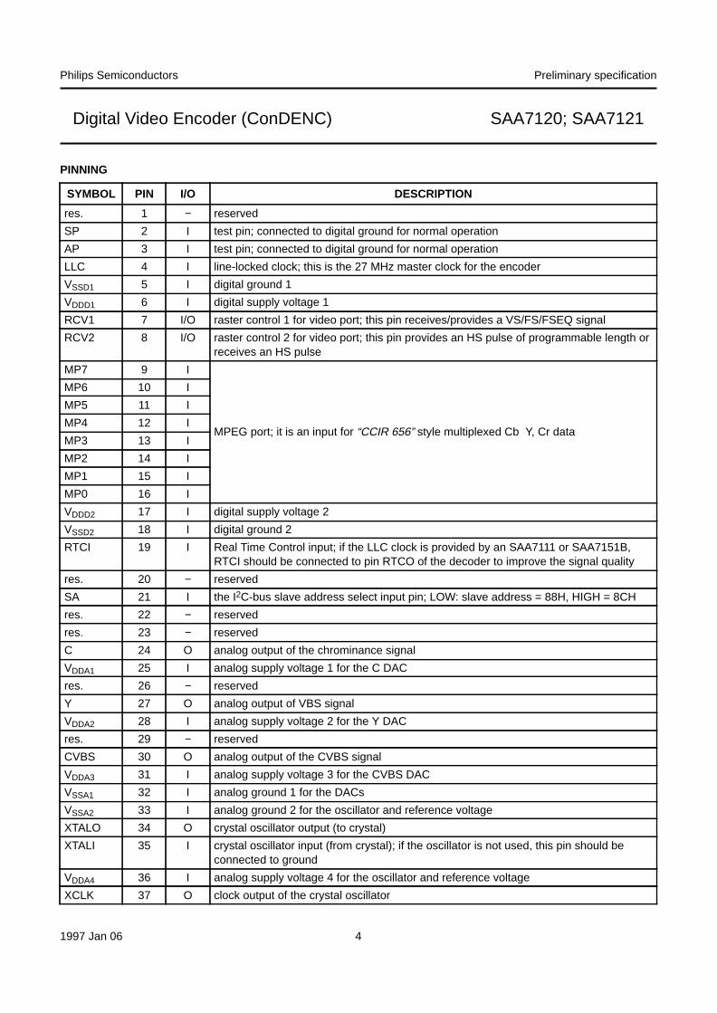
PINNING
SYMBOL PIN I/O DESCRIPTION
res. 1 − reserved
SP 2 I test pin; connected to digital ground for normal operation
AP 3 I test pin; connected to digital ground for normal operation
LLC 4 I line-locked clock; this is the 27 MHz master clock for the encoder
VSSD1 5 I digital ground 1
VDDD1 6 I digital supply voltage 1
RCV1 7 I/O raster control 1 for video port; this pin receives/provides a VS/FS/FSEQ signal
RCV2 8 I/O raster control 2 for video port; this pin provides an HS pulse of programmable length orreceives an HS pulse
MP7 9 I
MPEG port; it is an input for “CCIR 656” style multiplexed Cb Y, Cr data
MP6 10 I
MP5 11 I
MP4 12 I
MP3 13 I
MP2 14 I
MP1 15 I
MP0 16 I
VDDD2 17 I digital supply voltage 2
VSSD2 18 I digital ground 2
RTCI 19 I Real Time Control input; if the LLC clock is provided by an SAA7111 or SAA7151B,RTCI should be connected to pin RTCO of the decoder to improve the signal quality
res. 20 − reserved
SA 21 I the I2C-bus slave address select input pin; LOW: slave address = 88H, HIGH = 8CH
res. 22 − reserved
res. 23 − reserved
C 24 O analog output of the chrominance signal
VDDA1 25 I analog supply voltage 1 for the C DAC
res. 26 − reserved
Y 27 O analog output of VBS signal
VDDA2 28 I analog supply voltage 2 for the Y DAC
res. 29 − reserved
CVBS 30 O analog output of the CVBS signal
VDDA3 31 I analog supply voltage 3 for the CVBS DAC
VSSA1 32 I analog ground 1 for the DACs
VSSA2 33 I analog ground 2 for the oscillator and reference voltage
XTALO 34 O crystal oscillator output (to crystal)
XTALI 35 I crystal oscillator input (from crystal); if the oscillator is not used, this pin should beconnected to ground
VDDA4 36 I analog supply voltage 4 for the oscillator and reference voltage
XCLK 37 O clock output of the crystal oscillator

1997 Jan 06 5
Philips Semiconductors Preliminary specification
Digital Video Encoder (ConDENC) SAA7120; SAA7121
VSSD3 38 I digital ground 3
VDDD3 39 I digital supply voltage 3
RESET 40 I reset input, active LOW; after reset is applied, all digital I/Os are in input mode;the I2C-bus receiver waits for the START condition
SCL 41 I I2C-bus serial clock input
SDA 42 I/O I2C-bus serial data input/output
TTXRQ 43 O teletext request output, indicating when bit stream is valid
TTX 44 I teletext bit stream input
SYMBOL PIN I/O DESCRIPTION
Fig.2 Pin configuration.
handbook, full pagewidth
SAA7120 SAA7121
MBH790
1res.
SP
AP
LLC
VDDD1
VSSD1
RCV1
RCV2
MP7
MP6
MP5
MP
4
MP
3
MP
2
MP
1
MP
0
VD
DD
2
VS
SD
2
RT
CI
res. SA
res.
2
3
4
5
6
7
8
9
10
11
33 VSSA2
VSSA1
VDDA3
VDDA2
VDDA1
Y
C
CVBS
res.
res.
res.
32
31
30
29
28
27
26
25
24
23
12 13 14 15 16 17 18 19 20 21 22
44T
TX
TT
XR
Q
SD
A
SC
L
XC
LK
XT
ALI
XT
ALO
VD
DD
3
VD
DA
4
VS
SD
3
RE
SE
T
43 42 41 40 39 38 37 36 35 34

1997 Jan 06 6
Philips Semiconductors Preliminary specification
Digital Video Encoder (ConDENC) SAA7120; SAA7121
FUNCTIONAL DESCRIPTION
The digital video encoder (ConDENC) encodes digitalluminance and colour difference signals simultaneouslyinto analog CVBS and S-Video signals. NTSC-M,PAL B/G, and sub-standards are supported.
Both interlaced and non-interlaced operation is possiblefor all standards.
The basic encoder function consists of subcarriergeneration, colour modulation and the insertion ofsynchronization signals. Luminance and chrominancesignals are filtered in accordance with the standardrequirements of “RS-170-A” and “CCIR 624”.
For ease of analog post-filtering the signals areoversampled twice with respect to the pixel clock prior todigital-to-analog conversion.
The filter characteristics are shown in Figs 3 and 4.The DACs for Y, C, and CVBS have 10-bit resolution.
The 8-bit multiplexed Cb-Y-Cr formats are “CCIR 656”(D1 format) compatible, but the SAV and EAV codes can
be decoded optionally when the device is to operate inslave mode.
It is also possible to connect a Philips Digital VideoDecoder (SAA7111 or SAA7151B) to the ConDENC.Via pin RTCI, connected to RTCO of a decoder,information concerning the actual subcarrier, PAL-ID and(if used in conjunction with the SAA7111) the subcarrierphase can be inserted.
The ConDENC synthesizes all necessary internal signals,colour subcarrier frequency and synchronization signals.
Wide screen signalling data can be loaded via the I2C-bus.It is inserted into line 23 for 50 Hz field rate standards.
The IC contains closed caption and extended dataservices encoding (line 21), and supports anti-tapingsignal generation in accordance with Macrovision.
Possibilities are provided for setting video parameters:
Black and blanking level control
Colour subcarrier frequency
Variable burst amplitude.
handbook, full pagewidth
6
(1)
(2)
(4)
(3)
8 10 12 14
6
0
0 2 4
MGD672
−6
−12
−18
−30
−24
−36
−42
−54
−48
f (MHz)
Gv(dB)
Fig.3 Luminance transfer characteristic 1.
(1) CCRS1 = 0; CCRS0 = 1.
(2) CCRS1 = 1; CCRS0 = 0.
(3) CCRS1 = 0; CCRS0 = 0.
(4) CCRS1 = 1; CCRS0 = 1.

1997 Jan 06 7
Philips Semiconductors Preliminary specification
Digital Video Encoder (ConDENC) SAA7120; SAA7121
handbook, halfpage
0 2
(1)
6
1
0
−1
−2
−3
−4
−5
MBE736
4 f (MHz)
Gv(dB)
(1) CCRS1 = 0; CCRS0 = 0.
Fig.4 Luminance transfer characteristic 2.
During reset (RESET = LOW) and after reset is released,all digital I/O stages are set to input mode. A reset forcesthe I2C-bus interface to abort a running bus transfer andsets register 3A to 03H, register 61 to 06H,registers 6BH and 6EH to 00H and bit TTX60 to 0.All other control registers are not influenced by a reset.
Encoder
VIDEO PATH
The encoder generates out of Y, U and V basebandsignals luminance and colour subcarrier output signals,suitable for use as CVBS or separate Y and C signals.
Luminance is modified in gain and in offset (the latterprogrammable in a certain range to enable different blacklevel set-ups). A fixed synchronization level in accordancewith standard composite synchronization schemes isinserted. The inserted blanking level is programmable toallow for manipulations with Macrovision anti-taping.Additional insertion of AGC super-white pulses,programmable in height, is supported.
handbook, full pagewidth
6 8 10 12 14
6
0
0 2 4
MBE737
−6
−12
−18
−30
−24
−36
−42
−54
−48
f (MHz)
Gv(dB)
(1) (2)
(1) SCBW = 1.
(2) SCBW = 0.
Fig.5 Chrominance transfer characteristic 1.

1997 Jan 06 8
Philips Semiconductors Preliminary specification
Digital Video Encoder (ConDENC) SAA7120; SAA7121
In order to enable easy analog post-filtering, luminance isinterpolated from 13.5 MHz data rate to 27 MHz data rate,providing luminance in 10-bit resolution. This filter is alsoused to define smoothed transients for synchronizationpulses and blanking period. For transfer characteristic ofthe luminance interpolation filter see Figs 3 and 4.
Chrominance is modified in gain (programmableseparately for U and V), standard dependent burst isinserted, before baseband colour signals are interpolatedfrom 6.75 MHz data rate to 27 MHz data rate. One of theinterpolation stages can be bypassed, thus providing ahigher colour bandwidth, which can be made use of forY and C output. For transfer characteristics of thechrominance interpolation filter see Figs 5 and 6.
The amplitude, beginning and ending of inserted burst isprogrammable in a certain range, suitable for standardsignals and for special effects. Behind the succeedingquadrature modulator, colour in 10-bit resolution isprovided on subcarrier.
The numeric ratio between Y and C outputs is inaccordance with set standards.
TELETEXT INSERTION AND ENCODING
Pin TTX receives a WST- or NABTS-Teletext bitstreamsampled at the LLC clock. At each rising edge of output
(1) SCBW = 1.
(2) SCBW = 0.
handbook, halfpage
0 0.4 0.8 1.6
2
0
−4
−6
−2
MBE735
1.2 f (MHz)
Gv(dB)
(1)
(2)
Fig.6 Chrominance transfer characteristic 2.
signal TTXRQ a single teletext bit has to be provided aftera programmable delay at input pin.
Phase variant interpolation is achieved on this bitstream inthe internal teletext encoder, providing sufficient smallphase jitter on the output text lines.
TTXRQ provides a fully programmable request signal tothe teletext source, indicating the insertion period ofbitstream at lines selectable independently for both fields.The internal insertion window for text is set to 360(PAL-WST), 296 (NTSC-WST) or 288 (NABTS) teletextbits including clock run-in bits. For protocol and timingsee Fig.7.
CLOSED CAPTION ENCODER
Using this circuit, data in accordance with the specificationof closed caption or extended data service, delivered bythe control interface, can be encoded (Line 21).Two dedicated pairs of bytes (two bytes per field), eachpair preceded by run-in clocks and framing code, arepossible.
The actual line number where data is to be encoded in, canbe modified in a certain range.
Data clock frequency is in accordance with definition forNTSC-M standard 32 times horizontal line frequency.
Data LOW at the output of the DACs corresponds to 0 IRE,data HIGH at the output of the DACs corresponds toapproximately 50 IRE.
It is also possible to encode Closed Caption Data for 50 Hzfield frequencies at 32 times horizontal line frequency.
ANTI-TAPING (SAA7120 ONLY)
For more information contact your nearest PhilipsSemiconductors sales office.
Data manager
In the data manager, real time arbitration on the datastream to be encoded is performed.
A pre-defined colour look-up table located in this block canbe read out in a pre-defined sequence (8 steps per activevideo line), achieving a colour bar test pattern generatorwithout the need for an external data source. The colourbar function is under software control only.
Output interface/DACs
In the output interface encoded Y and C signals areconverted from digital to analog in 10-bit resolution.

1997 Jan 06 9
Philips Semiconductors Preliminary specification
Digital Video Encoder (ConDENC) SAA7120; SAA7121
Y and C signals are also combined to a 10-bit CVBSsignal.
The CVBS output occurs with the same processing delayas the Y and C outputs. Absolute amplitude at the input ofthe DAC for CVBS is reduced by 15⁄16 with respect toY and C DACs to make maximum use of conversionranges.
Outputs of the DACs can be set together in two groups viasoftware control to minimum output voltage for eitherpurpose.
Synchronization
Synchronization of the ConDENC is able to operate in twomodes; slave mode and master mode.
In the slave mode, the circuit accepts synchronizationpulses at the bidirectional RCV1 port. The timing andtrigger behaviour related to RCV1 can be influenced byprogramming the polarity and the on-chip delay of RCV1.Active slope of RCV1 defines the vertical phase andoptionally the odd/even and colour frame phase to beinitialized, it can be also used to set the horizontal phase.
If the horizontal phase is not to be influenced by RCV1, ahorizontal synchronization pulse needs to be supplied atthe pin RCV2. Timing and trigger behaviour can also beinfluenced by RCV2.
If there are missing pulses at RCV1 and/or RCV2, the timebase of ConDENC runs free, thus an arbitrary number ofsynchronization slopes may be absent, but no additionalpulses (with the incorrect phase) must occur.
If the vertical and horizontal phase is derived from RCV1,RCV2 can be used for horizontal or composite blankinginput or output.
Alternatively, the device can be triggered by auxiliarycodes in a “CCIR 656” data stream at the MP port.
In the master mode, the time base of the circuitcontinuously runs free. On the RCV1 port, the device canoutput:
• A Vertical Synchronisation signal (VS) with 3 or 2.5 linesduration, or
• An ODD/EVEN signal which is LOW in odd fields, or
• A field sequence signal (FSEQ) which is HIGH in the firstof 4 or 8 fields respectively.
On the RCV2 port, the device can provide a horizontalsynchronization pulse with programmable start and stopphase; this pulse can be inhibited in the vertical blankingperiod to build up, for example, a composite blankingsignal.
The polarity of both RCV1 and RCV2 is selectable bysoftware control.
The length of a field and the start and end of its active partcan be programmed. The active part of a field alwaysstarts at the beginning of a line.
Teletext timing
The teletext timing is shown in Fig.7. tFD is the time neededto interpolate input data TTX and inserting it into theCVBS and Y output signal, such that it appears attTTX = 10.2 µs (PAL) or tTTX = 10.5 µs (NTSC) after theleading edge of the horizontal synchronization pulse.
Time tPD is the pipeline delay time introduced by thesource that is gated by TTXRQ in order to deliver TTXdata. This delay is programmable by register TTXHD.For every active HIGH-state at output pin TTXRQ, a newteletext bit must be provided by the source.
Since the beginning of the pulses representing the TTXRQsignal and the delay between the rising edge of TTXRQand valid teletext input data are fully programmable(TTXHS and TTXHD), the TTX data is always inserted atthe correct position after the leading edge of outgoinghorizontal synchronization pulse.
Time tTTXWin is the internally used insertion window forTTX data; it has a constant length that allows insertion of360 teletext bits at a text data rate of 6.9375 Mbits/s(PAL), 296 teletext bits at a text data rate of 5.7272 Mbits/s(World Standard TTX) or 288 teletext bits at a text datarate of 5.7272 Mbits/s (NABTS). The insertion window isnot opened if the control bit TTXEN is logic 0.
Using appropriate programming, all suitable lines of theodd field (TTXOVS and TTXOVE) plus all suitable lines ofthe even field (TTXEVS and TTXEVE) can be used forteletext insertion.

1997 Jan 06 10
Philips Semiconductors Preliminary specification
Digital Video Encoder (ConDENC) SAA7120; SAA7121
Fig.7 Teletext timing.
handbook, full pagewidth
tTTXWintTTX
tPD tFD
CVBS/Y
TTX
TTXRQ
textbit #: 1 2 3 4 5 6 7 8 9 10 11 12 13 14 15 16 17 18 19 20 21 22 23 24
MBH788
Analog output voltages
The analog output voltages are dependent on theopen-loop voltage of the operational amplifiers forfull-scale conversion (typical value 1.35 V), the internalseries resistor (typical value 2 Ω), the external seriesresistor and the external load impedance.
The digital output signals in front of the DACs undernominal conditions occupy different conversion ranges, asindicated in Table 1 for a 100⁄100 colour bar signal.
Values for the external series resistors result in a 75 Ωload.
Input levels and formats
The ConDENC expects digital Y, Cb, Cr data with levels(digital codes) in accordance with “CCIR 601” (seeTables 2 and 3).
For C and CVBS outputs, deviating amplitudes of thecolour difference signals can be compensated byindependent gain control setting, while gain for luminanceis set to predefined values, distinguishable for 7.5 IREset-up or without set-up.
Reference levels are measured with a colour bar,100% white, 100% amplitude and 100% saturation.
Table 1 Digital output signals conversion range
Table 2 “CCIR 601” signal component levels
CONVERSION RANGE (peak-to-peak) (digits)
CVBS, SYNCTIP-TO-PEAK CARRIER
Y (VBS) SYNCTIP-TO-WHITE
1016 881
COLOURSIGNALS
Y Cb Cr
White 235 128 128
Yellow 210 16 146
Cyan 170 166 16
Green 145 54 34
Magenta 106 202 222
Red 81 90 240
Blue 41 240 110
Black 16 128 128

1997 Jan 06 11
Philips Semiconductors Preliminary specification
Digital Video Encoder (ConDENC) SAA7120; SAA7121
I2C-bus interface
The I2C-bus interface is a standard slave transceiver,supporting 7-bit slave addresses and 400 kbits/sguaranteed transfer rate. It uses 8-bit subaddressing withan auto-increment function. All registers are write only,except one readable status byte.
Two I2C-bus slave addresses are present:
88H: LOW at pin SA
8CH: HIGH at pin SA.
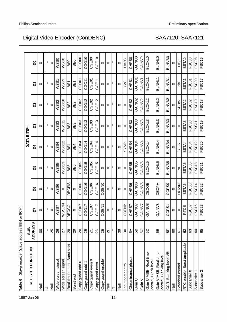
Tables 5 and 4 summarize the format of the I2C-busaddressing. For more information on how to use theI2C-bus see “The I2C-bus and how to use it”, orderno. 9398 393 40011. Tables 7 to 42 contain theprogramming information for the subaddresses. Table 6summarises this information.
Table 3 8-bit multiplexed format (similar to “CCIR 601”)
Table 4 I2C-bus address format; see Table 5
Table 5 Explanation of Table 4
Notes
1. x is the read/write control bit; write:x = logic 0;read: x = logic 1, no subaddressing with read.
2. If more than 1 byte DATA is transmitted, then auto-increment of the subaddress is performed.
BITS
0 1 2 2 4 5 6 7
Sample Cb0 Y0 Cr0 Y1 Cb2 Y2 Cr2 Y3
Luminance pixel number 0 1 2 3
Colour pixel number 0 2
S SLAVE ADDRESS ACK SUBADDRESS ACK DATA 0 ACK -------- DATA n ACK P
PART DESCRIPTION
S START condition
Slave address 1 0 0 0 1 0 0 x or 1 0 0 0 1 1 0 x (1)
ACK acknowledge, generated by the slave
Subaddress(2) subaddress byte
DATA data byte
-------- continued data bytes and ACKs
P STOP condition
1997 Jan 06 12
Philips Semiconductors Preliminary specification
Digital Video Encoder (ConDENC) SAA7120; SAA7121
Tabl
e 6
Sla
ve r
ecei
ver
(sla
ve a
ddre
ss 8
8Hor
8CH
)
RE
GIS
TE
R F
UN
CT
ION
SU
BA
DD
RE
SS
DAT
A B
ITS
(1)
D7
D6
D5
D4
D3
D2
D1
D0
Nul
l00
00
00
00
00
⋅⋅
⋅⋅
⋅⋅
⋅⋅
⋅⋅
Nul
l25
00
00
00
00
Wid
e sc
reen
sig
nal
26W
SS
7W
SS
6W
SS
5W
SS
4W
SS
3W
SS
2W
SS
1W
SS
0
Wid
e sc
reen
sig
nal
27W
SS
ON
0W
SS
13W
SS
12W
SS
11W
SS
10W
SS
9W
SS
8
Rea
l tim
e co
ntro
l, B
urst
sta
rt28
DE
CC
OL
DE
CF
ISB
S5
BS
4B
S3
BS
2B
S1
BS
0
Bur
st e
nd29
00
BE
5B
E4
BE
3B
E2
BE
1B
E0
Cop
y gu
ard
odd
02A
CG
O07
CG
O06
CG
O05
CG
O04
CG
O03
CG
O02
CG
O01
CG
O00
Cop
y gu
ard
odd
12B
CG
O17
CG
O16
CG
O15
CG
O14
CG
O13
CG
O12
CG
O11
CG
O10
Cop
y gu
ard
even
02C
CG
E07
CG
E06
CG
E05
CG
E04
CG
E03
CG
E02
CG
E01
CG
E00
Cop
y gu
ard
even
12D
CG
E17
CG
E16
CG
E15
CG
E14
CG
E13
CG
E12
CG
E11
CG
E10
Cop
y gu
ard
enab
le2E
CG
EN
1C
GE
N0
00
00
00
Nul
l2F
00
00
00
00
⋅⋅
⋅⋅
⋅⋅
⋅⋅
⋅⋅
Nul
l39
00
00
00
00
Inpu
t por
t con
trol
3AC
BE
NB
00
SY
MP
00
Y2C
UV
2C
Chr
omin
ance
pha
se5A
CH
PS
7C
HP
S6
CH
PS
5C
HP
S4
CH
PS
3C
HP
S2
CH
PS
1C
HP
S0
Gai
nU
5BG
AIN
U7
GA
INU
6G
AIN
U5
GA
INU
4G
AIN
U3
GA
INU
2G
AIN
U1
GA
INU
0
Gai
nV
5CG
AIN
V7
GA
INV
6G
AIN
V5
GA
INV
4G
AIN
V3
GA
INV
2G
AIN
V1
GA
INV
0
Gai
nU
MS
B, R
eal t
ime
cont
rol,
Bla
ck le
vel
5DG
AIN
U8
DE
CO
EB
LCK
L5B
LCK
L4B
LCK
L3B
LCK
L2B
LCK
L1B
LCK
L0
Gai
nV
MS
B, R
eal t
ime
cont
rol,
Bla
nkin
g le
vel
5EG
AIN
V8
DE
CP
HB
LNN
L5B
LNN
L4B
LNN
L3B
LNN
L2B
LNN
L1B
LNN
L0
CC
R, B
lank
ing
leve
l VB
I5F
CC
RS
1C
CR
S0
BLN
VB
5B
LNV
B4
BLN
VB
3B
LNV
B2
BLN
VB
1B
LNV
B0
Nul
l60
00
00
00
00
Sta
ndar
d co
ntro
l61
0D
OW
NIN
PI
YG
S0
SC
BW
PA
LF
ISE
RT
C e
nabl
e, B
urst
am
plitu
de62
RT
CE
BS
TA6
BS
TA5
BS
TA4
BS
TA3
BS
TA2
BS
TA1
BS
TA0
Sub
carr
ier
063
FS
C07
FS
C06
FS
C05
FS
C04
FS
C03
FS
C02
FS
C01
FS
C00
Sub
carr
ier
164
FS
C15
FS
C14
FS
C13
FS
C12
FS
C11
FS
C10
FS
C09
FS
C08
Sub
carr
ier
265
FS
C23
FS
C22
FS
C21
FS
C20
FS
C19
FS
C18
FS
C17
FS
C16

1997 Jan 06 13
Philips Semiconductors Preliminary specification
Digital Video Encoder (ConDENC) SAA7120; SAA7121
Not
e
1.A
ll bi
ts la
belle
d ‘0
’ are
res
erve
d. T
hey
mus
t be
pro
gram
med
with
logi
c 0.
Sub
carr
ier
366
FS
C31
FS
C30
FS
C29
FS
C28
FS
C27
FS
C26
FS
C25
FS
C24
Line
21 o
dd0
67L2
1O07
L21O
06L2
1O05
L21O
04L2
1O03
L21O
02L2
1O01
L21O
00
Line
21 o
dd1
68L2
1O17
L21O
16L2
1O15
L21O
14L2
1O13
L21O
12L2
1O11
L21O
10
Line
21 e
ven
069
L21E
07L2
1E06
L21E
05L2
1E04
L21E
03L2
1E02
L21E
01L2
1E00
Line
21 e
ven
16A
L21E
17L2
1E16
L21E
15L2
1E14
L21E
13L2
1E12
L21E
11L2
1E10
RC
V p
ort c
ontr
ol6B
SR
CV
11S
RC
V10
TR
CV
2O
RC
V1
PR
CV
1C
BLF
OR
CV
2P
RC
V2
Trig
ger
cont
rol
6CH
TR
IG7
HT
RIG
6H
TR
IG5
HT
RIG
4H
TR
IG3
HT
RIG
2H
TR
IG1
HT
RIG
0
Trig
ger
cont
rol
6DH
TR
IG10
HT
RIG
9H
TR
IG8
VT
RIG
4V
TR
IG3
VT
RIG
2V
TR
IG1
VT
RIG
0
Mul
ti co
ntro
l6E
SB
LBN
0P
HR
ES
1P
HR
ES
00
0F
LC1
FLC
O
Clo
sed
capt
ion,
Tele
text
ena
ble
6FC
CE
N1
CC
EN
0T
TX
EN
SC
CLN
4S
CC
LN3
SC
CLN
2S
CC
LN1
SC
CLN
0
RC
V2
outp
ut s
tart
70R
CV
2S7
RC
V2S
6R
CV
2S5
RC
V2S
4R
CV
2S3
RC
V2S
2R
CV
2S1
RC
V2S
0
RC
V2
outp
ut e
nd71
RC
V2E
7R
CV
2E6
RC
V2E
5R
CV
2E4
RC
V2E
3R
CV
2E2
RC
V2E
1R
CV
2E0
MS
Bs
RC
V2
outp
ut72
0R
CV
2E10
RC
V2E
9R
CV
2E8
0R
CV
2S10
RC
V2S
9R
CV
2S8
TT
X r
eque
st H
sta
rt73
TT
XH
S7
TT
XH
S6
TT
XH
S5
TT
XH
S4
TT
XH
S3
TT
XH
S2
TT
XH
S1
TT
XH
S0
TT
X r
eque
st H
del
ay74
TT
XH
D7
TT
XH
D6
TT
XH
D5
TT
XH
D4
TT
XH
D3
TT
XH
D2
TT
XH
D1
TT
XH
D0
V-S
ync
shift
750
00
00
VS
_S2
VS
_S1
VS
_S0
TT
X o
dd r
eque
st V
S76
TT
XO
VS
7T
TX
OV
S6
TT
XO
VS
5T
TX
OV
S4
TT
XO
VS
3T
TX
OV
S2
TT
XO
VS
1T
TX
OV
S0
TT
X o
dd r
eque
st V
E77
TT
XO
VE
7T
TX
OV
E6
TT
XO
VE
5T
TX
OV
E4
TT
XO
VE
3T
TX
OV
E2
TT
XO
VE
1T
TX
OV
E0
TT
X e
ven
requ
est V
S78
TT
XE
VS
7T
TX
EV
S6
TT
XE
VS
5T
TX
EV
S4
TT
XE
VS
3T
TX
EV
S2
TT
XE
VS
1T
TX
EV
S0
TT
X e
ven
requ
est V
E79
TT
XE
VE
7T
TX
EV
E6
TT
XE
VE
5T
TX
EV
E4
TT
XE
VE
3T
TX
EV
E2
TT
XE
VE
1T
TX
EV
E0
Firs
t act
ive
line
7AFA
L7FA
L6FA
L5FA
L4FA
L3FA
L2FA
L1FA
L0
Last
act
ive
line
7BLA
L7LA
L6LA
L5LA
L4LA
L3LA
L2LA
L1LA
L0
MS
B v
ertic
al7C
TT
X60
LAL8
0FA
L8T
TX
EV
E8
TT
XO
VE
8T
TX
EV
S8
TT
XO
VS
8
Nul
l7D
00
00
00
00
Dis
able
TT
X li
ne7E
LIN
E12
LIN
E11
LIN
E10
LIN
E9
LIN
E8
LIN
E7
LIN
E6
LIN
E5
Dis
able
TT
X li
ne7F
LIN
E20
LIN
E19
LIN
E18
LIN
E17
LIN
E16
LIN
E15
LIN
E14
LIN
E13
RE
GIS
TE
R F
UN
CT
ION
SU
BA
DD
RE
SS
DAT
A B
ITS
(1)
D7
D6
D5
D4
D3
D2
D1
D0

1997 Jan 06 14
Philips Semiconductors Preliminary specification
Digital Video Encoder (ConDENC) SAA7120; SAA7121
Slave Receiver
Table 7 Subaddress 26 and 27
Table 8 Subaddress 28 and 29
Table 9 Subaddress 2A to 2D
Table 10 Subaddress 2E
DATA BYTELOGICLEVEL
DESCRIPTION
WSS − wide screen signalling bits: 13 to 11 = reserved
10 to 8 = subtitles
7 to 4 = enhanced services
3 to 0 = aspect ratio
WSSON 0 wide screen signalling output is disabled
1 wide screen signalling output is enabled
DATA BYTELOGICLEVEL
DESCRIPTION REMARKS
BS − starting point of burst in clock cycles PAL : BS = 33 (21H)
NTSC : BS = 25 (19H)
BE − ending point of burst in clock cycles PAL : BS = 29 (1DH)
NTSC : BS = 29 (1DH)
DECCOL 0 disable colour detection bit of RTCI input
1 enable colour detection bit of RTCI input bit RTCE must be set to 1 (see Fig.10)
DECFIS 0 field sequence as FISE in subaddress 61
1 field sequence as FISE bit in RTCI input bit RTCE must be set to 1 (see Fig.10)
DATA BYTE DESCRIPTION REMARKS
CGO0 first byte of Copy guard data, odd field LSBs of the respective bytes are encodedimmediately after run-in and framing code, theMSBs of the respective bytes have to carry theparity bit, in accordance with the definition ofLine 20 encoding format.
CGO1 second byte of Copy guard data, odd field
CGE0 first byte of Copy guard data, even field
CGE1 second byte of Copy guard data, even field
DATA BYTEDESCRIPTION
CCEN1 CCEN0
0 0 copy guard encoding off
0 1 enables encoding in field 1 (odd)
1 0 enables encoding in field 2 (even)
1 1 enables encoding in both fields

1997 Jan 06 15
Philips Semiconductors Preliminary specification
Digital Video Encoder (ConDENC) SAA7120; SAA7121
Table 11 Subaddress 3A
Table 12 Subaddress 5A
Remark : in subaddresses 5B, 5C, 5D, 5E and 62 all IRE values are rounded up.
Table 13 Subaddress 5B and 5D
Table 14 Subaddress 5C and 5E
DATA BYTELOGICLEVEL
DESCRIPTION
UV2C 0 Cb, Cr data are two’s complement
1 Cb, Cr data are straight binary; default after reset
Y2C 0 Y data is two’s complement
1 Y data is straight binary; default after reset
SYMP 0 horizontal and vertical trigger is taken from RCV2 and RCV1 respectively; default after reset
1 horizontal and vertical trigger is decoded out of “CCIR 656” compatible data at MP port
CBENB 0 data from input ports is encoded; default after reset
1 colour bar with fixed colours is encoded
DATA BYTE DESCRIPTION VALUE RESULT
CHPS phase of encoded colour subcarrier(including burst) relative to horizontal sync;can be adjusted in steps of360/256 degrees
3FH PAL-B/G and data from input ports
69H PAL-B/G and data from look-up table
67H NTSC-M and data from input ports
89H NTSC-M and data from look-up table
DATA BYTE DESCRIPTION CONDITIONS REMARKS
GAINU variable gain forCb signal; inputrepresentationaccordance with“CCIR 601”
white-to-black = 92.5 IRE GAINU = −2.17 × nominal to +2.16 × nominal
GAINU = 0 output subcarrier of U contribution = 0
GAINU = 118 (76H) output subcarrier of U contribution = nominal
white-to-black = 100 IRE GAINU = −2.05 × nominal to +2.04 × nominal
GAINU = 0 output subcarrier of U contribution = 0
GAINU = 125 (7DH) output subcarrier of U contribution = nominal
DATA BYTE DESCRIPTION CONDITIONS REMARKS
GAINV variable gain forCr signal; inputrepresentationaccordance with“CCIR 601”
white-to-black = 92.5 IRE GAINV = −1.55 × nominal to +1.55 × nominal
GAINV = 0 output subcarrier of V contribution = 0
GAINV = 165 (A5H) output subcarrier of V contribution = nominal
white-to-black = 100 IRE GAINV = −1.46 × nominal to +1.46 × nominal
GAINV = 0 output subcarrier of V contribution = 0
GAINV = 175 (AFH) output subcarrier of V contribution = nominal

1997 Jan 06 16
Philips Semiconductors Preliminary specification
Digital Video Encoder (ConDENC) SAA7120; SAA7121
Table 15 Subaddress 5D
Notes
1. Output black level/IRE = BLCKL × 2/6.29 + 34.0
2. Output black level/IRE = BLCKL × 2/6.18 + 31.7
Table 16 Subaddress 5E
Notes
1. Output black level/IRE = BLNNL × 2/6.29 + 25.4
2. Output black level/IRE = BLNNL × 2/6.18 + 25.9
Table 17 Subaddress 5F
Table 18 Logic levels and function of CCRS
DATA BYTE DESCRIPTION CONDITIONS REMARKS
BLCKL variable black level; inputrepresentationaccordance with“CCIR 601”
white-to-sync = 140 IRE(1) recommended value: BLCKL = 42 (2AH)
BLCKL = 0 output black level = 34 IRE
BLCKL = 63 (3FH) output black level = 54 IRE
white-to-sync = 143 IRE(2) recommended value: BLCKL = 35 (23H)
BLCKL = 0 output black level = 32 IRE
BLCKL = 63 (3FH) output black level = 52 IRE
DECOE real time control logic 0 disable odd/even field control bit from RTCI
logic 1 enable odd/even field control bit from RTCI(see Fig.10)
DATA BYTE DESCRIPTION CONDITIONS REMARKS
BLNNL variable blanking level white-to-sync = 140 IRE(1) recommended value: BLNNL = 46 (2EH)
BLNNL = 0 output blanking level = 25 IRE
BLNNL = 63 (3FH) output blanking level = 45 IRE
white-to-sync = 143 IRE(2) recommended value: BLNNL = 53 (35H)
BLNNL = 0 output blanking level = 26 IRE
BLNNL = 63 (3FH) output blanking level = 46 IRE
DECPH real time control logic 0 disable subcarrier phase reset bit from RTCI
logic 1 enable subcarrier phase reset bit from RTCI(see Fig.10)
DATA BYTE DESCRIPTION
BLNVB variable blanking level during vertical blanking interval is typically identical to value of BLNNL
CCRS select cross colour reduction filter in luminance; see Table 18
CCRS1 CCRS0 DESCRIPTION
0 0 no cross colour reduction; for overall transfer characteristic of luminance see Fig.3
0 1 cross colour reduction #1 active; for overall transfer characteristic see Fig.3
1 0 cross colour reduction #2 active; for overall transfer characteristic see Fig.3
1 1 cross colour reduction #3 active; for overall transfer characteristic see Fig.3

1997 Jan 06 17
Philips Semiconductors Preliminary specification
Digital Video Encoder (ConDENC) SAA7120; SAA7121
Table 19 Subaddress 61
Table 20 Subaddress 62H
Table 21 Subaddress 62H
DATA BYTELOGICLEVEL
DESCRIPTION
FISE 0 864 total pixel clocks per line; default after reset
1 858 total pixel clocks per line
PAL 0 NTSC encoding (non-alternating V component)
1 PAL encoding (alternating V component); default after reset
SCBW 0 enlarged bandwidth for chrominance encoding (for overall transfer characteristic ofchrominance in baseband representation see Figs 3 and 4)
1 standard bandwidth for chrominance encoding (for overall transfer characteristic ofchrominance in baseband representation see Figs 3 and 4); default after reset
YGS 0 luminance gain for white − black 100 IRE; default after reset
1 luminance gain for white − black 92.5 IRE including 7.5 IRE set-up of black
INPI 0 PAL switch phase is nominal; default after reset
1 PAL switch phase is inverted compared to nominal
DOWN 0 DACs for CVBS, Y and C in normal operational mode; default after reset
1 DACs for CVBS, Y and C forced to lowest output voltage
DATA BYTELOGICLEVEL
DESCRIPTION
RTCE 0 no real time control of generated subcarrier frequency
1 real time control of generated subcarrier frequency through SAA7151B or SAA7111(timing see Fig.10)
DATA BYTE DESCRIPTION CONDITIONS REMARKS
BSTA amplitude of colour burst; inputrepresentation in accordancewith “CCIR 601”
white-to-black = 92.5 IRE;burst = 40 IRE; NTSC encoding
recommended value:BSTA = 63 (3FH)
BSTA = 0 to 2.02 × nominal
white-to-black = 92.5 IRE;burst = 40 IRE; PAL encoding
recommended value:BSTA = 45 (2DH)
BSTA = 0 to 2.82 × nominal
white-to-black = 100 IRE;burst = 43 IRE; NTSC encoding
recommended value:BSTA = 67 (43H)
BSTA = 0 to 1.90 × nominal
white-to-black = 100 IRE;burst = 43 IRE; PAL encoding
recommended value:BSTA = 47 (2FH)
BSTA = 0 to 3.02 × nominal

1997 Jan 06 18
Philips Semiconductors Preliminary specification
Digital Video Encoder (ConDENC) SAA7120; SAA7121
Table 22 Subaddress 63 to 66 (four bytes to program subcarrier frequency)
Note
1. Examples:
a) NTSC-M: ffsc = 227.5, fllc = 1716 → FSC = 569408543 (21F07C1FH).
b) PAL-B/G: ffsc = 283.7516, fllc = 1728 → FSC = 705268427 (2A098ACBH).
Table 23 Subaddress 67 to 6A
Table 24 Subaddress 6B
DATA BYTE DESCRIPTION CONDITIONS REMARKS
FSC0 to FSC3 ffsc = subcarrier frequency (inmultiples of line frequency);fllc = clock frequency (in multiplesof line frequency)
,
rounded up; see note 1
FSC3 = most significant byteFSC0 = least significant byte
DATA BYTE DESCRIPTION REMARKS
L21O0 first byte of captioning data, odd field LSBs of the respective bytes are encodedimmediately after run-in and framing code, theMSBs of the respective bytes have to carry theparity bit, in accordance with the definition ofLine 21 encoding format.
L21O1 second byte of captioning data, odd field
L21E0 first byte of extended data, even field
L21E1 second byte of extended data, even field
DATA BYTELOGICLEVEL
DESCRIPTION
PRCV2 0 polarity of RCV2 as output is active HIGH, rising edge is taken when input, respectively;default after reset
1 polarity of RCV2 as output is active LOW, falling edge is taken when input, respectively
ORCV2 0 pin RCV2 is switched to input; default after reset
1 pin RCV2 is switched to output
CBLF 0 if ORCV2 = HIGH, pin RCV2 provides an HREF signal (Horizontal Reference pulse that isdefined by RCV2S and RCV2E, also during vertical blanking Interval); default after reset
if ORCV2 = LOW and bit SYMP = LOW, signal input to RCV2 is used for horizontalsynchronization only (if TRCV2 = 1); default after reset
1 if ORCV2 = HIGH, pin RCV2 provides a ‘Composite-Blanking-Not’ signal, for example areference pulse that is defined by RCV2S and RCV2E, excluding Vertical Blanking Interval,which is defined by FAL and LAL
if ORCV2 = LOW and bit SYMP = LOW, signal input to RCV2 is used for horizontalsynchronization (if TRCV2 = 1) and as an internal blanking signal
PRCV1 0 polarity of RCV1 as output is active HIGH, rising edge is taken when input; default after reset
1 polarity of RCV1 as output is active LOW, falling edge is taken when input
ORCV1 0 pin RCV1 is switched to input; default after reset
1 pin RCV1 is switched to output
TRCV2 0 horizontal synchronization is taken from RCV1 port (at bit SYMP = LOW) or from decodedframe sync of “CCIR 656” input (at bit SYMP = HIGH); default after reset
1 horizontal synchronization is taken from RCV2 port (at bit SYMP = LOW)
SRCV1 − defines signal type on pin RCV1; see Table 25
FSCffsc
fllc-------- 2
32×
=
1997 Jan 06 19
Philips Semiconductors Preliminary specification
Digital Video Encoder (ConDENC) SAA7120; SAA7121
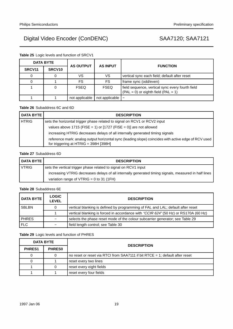
Table 25 Logic levels and function of SRCV1
Table 26 Subaddress 6C and 6D
Table 27 Subaddress 6D
Table 28 Subaddress 6E
Table 29 Logic levels and function of PHRES
DATA BYTEAS OUTPUT AS INPUT FUNCTION
SRCV11 SRCV10
0 0 VS VS vertical sync each field; default after reset
0 1 FS FS frame sync (odd/even)
1 0 FSEQ FSEQ field sequence, vertical sync every fourth field(PAL = 0) or eighth field (PAL = 1)
1 1 not applicable not applicable −
DATA BYTE DESCRIPTION
HTRIG sets the horizontal trigger phase related to signal on RCV1 or RCV2 input
values above 1715 (FISE = 1) or [1727 (FISE = 0)] are not allowed
increasing HTRIG decreases delays of all internally generated timing signals
reference mark: analog output horizontal sync (leading slope) coincides with active edge of RCV usedfor triggering at HTRIG = 398H [398H]
DATA BYTE DESCRIPTION
VTRIG sets the vertical trigger phase related to signal on RCV1 input
increasing VTRIG decreases delays of all internally generated timing signals, measured in half lines
variation range of VTRIG = 0 to 31 (1FH)
DATA BYTELOGICLEVEL
DESCRIPTION
SBLBN 0 vertical blanking is defined by programming of FAL and LAL; default after reset
1 vertical blanking is forced in accordance with “CCIR 624” (50 Hz) or RS170A (60 Hz)
PHRES − selects the phase reset mode of the colour subcarrier generator; see Table 29
FLC − field length control; see Table 30
DATA BYTEDESCRIPTION
PHRES1 PHRES0
0 0 no reset or reset via RTCI from SAA7111 if bit RTCE = 1; default after reset
0 1 reset every two lines
1 0 reset every eight fields
1 1 reset every four fields
1997 Jan 06 20
Philips Semiconductors Preliminary specification
Digital Video Encoder (ConDENC) SAA7120; SAA7121
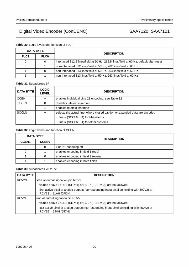
Table 30 Logic levels and function of FLC
Table 31 Subaddress 6F
Table 32 Logic levels and function of CCEN
Table 33 Subaddress 70 to 72
DATA BYTEDESCRIPTION
FLC1 FLC0
0 0 interlaced 312.5 lines/field at 50 Hz, 262.5 lines/field at 60 Hz; default after reset
0 1 non-interlaced 312 lines/field at 50 Hz, 262 lines/field at 60 Hz
1 0 non-interlaced 313 lines/field at 50 Hz, 263 lines/field at 60 Hz
1 1 non-interlaced 313 lines/field at 50 Hz, 263 lines/field at 60 Hz
DATA BYTELOGICLEVEL
DESCRIPTION
CCEN − enables individual Line 21 encoding; see Table 32
TTXEN 0 disables teletext insertion
1 enables teletext insertion
SCCLN − selects the actual line, where closed caption or extended data are encoded
line = (SCCLN + 4) for M-systems
line = (SCCLN + 1) for other systems
DATA BYTEDESCRIPTION
CCEN1 CCEN0
0 0 Line 21 encoding off
0 1 enables encoding in field 1 (odd)
1 0 enables encoding in field 2 (even)
1 1 enables encoding in both fields
DATA BYTE DESCRIPTION
RCV2S start of output signal on pin RCV2
values above 1715 (FISE = 1) or [1727 (FISE = 0)] are not allowed
first active pixel at analog outputs (corresponding input pixel coinciding with RCV2) atRCV2S = 11AH [0FDH]
RCV2E end of output signal on pin RCV2
values above 1715 (FISE = 1) or [1727 (FISE = 0)] are not allowed
last active pixel at analog outputs (corresponding input pixel coinciding with RCV2) atRCV2E = 694H [687H]

1997 Jan 06 21
Philips Semiconductors Preliminary specification
Digital Video Encoder (ConDENC) SAA7120; SAA7121
Table 34 Subaddress 73 and 74
Table 35 Subaddress 75
Table 36 Subaddress 76, 77 and 7C
Table 37 Subaddress 78, 79 and 7C
Table 38 Subaddress 7C
Table 39 Subaddress 7A to 7C
DATA BYTE DESCRIPTION
TTXHS start of signal on pin TTXRQ see Fig.7
TTXHD indicates the delay in clock cycles between rising edge of TTXRQ output and valid data on pin TTXminimum value has to be TTXHD = 2
DATA BYTE DESCRIPTION
VS_S Vertical Sync. shift between RCV1 and RCV2 (switched to output) in master mode it is possible to shiftH-sync (RCV2; CBLF = 0) against V-sync (RCV1; SRCV1 = 00)
standard value: VS_S = 3
DATA BYTE DESCRIPTION
TTXOVS first line of occurrence of signal on pin TTXRQ in odd field
line = (TTXOVS + 4) for M-systems
line = (TTXOVS + 1) for other systems
TTXOVE last line of occurrence of signal on pin TTXRQ in odd field
line = (TTXOVE + 3) for M-systems
line = TTXOVE for other systems
DATA BYTE DESCRIPTION
TTXEVS first line of occurrence of signal on pin TTXRQ in even field
line = (TTXEVS + 4) for M-systems
line = (TTXEVS + 1) for other systems
TTXEVE last line of occurrence of signal on pin TTXRQ in even field
line = (TTXEVE + 3) for M-systems
line = TTXEVE for other systems
DATA BYTELOGICLEVEL
DESCRIPTION
TTX60 0 enables NABTS (FISE = 1) or European TTX (FISE = 0); default after reset
1 enables World Standard Teletext 60 Hz (FISE = 1)
DATA BYTE DESCRIPTION
FAL first active line = FAL + 4 for M-systems, = FAL + 1 for other systems, measured in lines FAL = 0coincides with the first field synchronization pulse
LAL last active line = LAL + 3 for M-systems, = LAL for other system, measured in lines LAL = 0 coincideswith the first field synchronization pulse

1997 Jan 06 22
Philips Semiconductors Preliminary specification
Digital Video Encoder (ConDENC) SAA7120; SAA7121
Table 40 Subaddress 7E and 7F
Slave Transmitter
Table 41 Slave transmitter (slave address 89H or 8DH)
Table 42 No subaddress
DATA BYTE DESCRIPTION
LINE individual lines in both fields (PAL counting) can be disabled for insertion of teletext by the respectivebits, disabled line = LINExx (50 Hz field rate)
this bit mask is effective only, if the lines are enabled by TTXOVS/TTXOVE and TTXEVS/TTXEVE
REGISTERFUNCTION
SUBADDRESSDATA BYTE
D7 D6 D5 D4 D3 D2 D1 D0
Status byte − VER2 VER1 VER0 CCRDO CCRDE 0 FSEQ O_E
DATA BYTELOGICLEVEL
DESCRIPTION
VER − Version identification of the device. It will be changed with all versions of the device thathave different programming models. Current version is 000 binary.
CCRDO 1 Closed caption bytes of the odd field have been encoded.
0 The bit is reset after information has been written to the subaddresses 67 and 68. It is setimmediately after the data has been encoded.
CCRDE 1 Closed caption bytes of the even field have been encoded.
0 The bit is reset after information has been written to the subaddresses 69 and 6A. It is setimmediately after the data has been encoded.
FSEQ 1 During first field of a sequence (repetition rate: NTSC = 4 fields, PAL = 8 fields).
0 Not first field of a sequence.
O_E 1 During even field.
0 During odd field.

1997 Jan 06 23
Philips Semiconductors Preliminary specification
Digital Video Encoder (ConDENC) SAA7120; SAA7121
CHARACTERISTICSVDDD = 3.0 to 3.6 V; Tamb = 0 to +70 °C; unless otherwise specified.
SYMBOL PARAMETER CONDITIONS MIN. MAX. UNIT
Supply
VDDA analog supply voltage 3.1 3.5 V
VDDD digital supply voltage 3.0 3.6 V
IDDA analog supply current note 1 − 62 mA
IDDD digital supply current note 1 − 38 mA
Inputs
VIL LOW level input voltage(except SDA, SCL, AP, SP and XTALI)
−0.5 +0.8 V
VIH HIGH level input voltage(except, SDA, SCL, AP, SP and XTALI)
2.0 VDDD + 0.3 V
ILI input leakage current − 1 µA
Ci input capacitance clocks − 10 pF
data − 8 pF
I/Os at high impedance − 8 pF
Outputs
VOL LOW level output voltage(except SDA and XTALO)
IOL = 4 mA − 0.4 V
VOH HIGH level output voltage(except, SDA, and XTALO)
IOH = 4 mA VDDD − 4 − V
I2C-bus; SDA and SCL
VIL LOW level input voltage −0.5 VDDD + 0.3 V
VIH HIGH level input voltage 2.3 VDDD + 0.3 V
Ii input current Vi = LOW or HIGH −10 +10 µA
VOL LOW level output voltage (SDA) IOL = 3 mA − 0.4 V
Io output current during acknowledge 3 − mA
Clock timing (LLC)
TLLC cycle time note 2 34 41 ns
δ duty factor tHIGH/tLLC note 3 40 60 %
tr rise time note 2 − 5 ns
tf fall time note 2 − 6 ns
Input timing
tSU;DAT input data set-up time (any pin exceptSCL, SDA, RESET, AP and SP)
6 − ns
tHD;DAT input data hold time (any pin exceptSCL, SDA, RESET, AP and SP)
3 − ns

1997 Jan 06 24
Philips Semiconductors Preliminary specification
Digital Video Encoder (ConDENC) SAA7120; SAA7121
Notes
1. At maximum supply voltage with highly active input signals.
2. The data is for both input and output direction.
3. With LLC in input mode. In output mode, with a crystal connected to XTALO/XTALI duty factor is typically 50%.
4. If an internal oscillator is used, crystal deviation of nominal frequency is directly proportional to the deviation ofsubcarrier frequency and line/field frequency.
5. For full digital range, without load, VDDA = 3.3 V. The typical voltage swing is 1.35 V, the typical minimum outputvoltage (digital zero at DAC) is 0.2 V.
Crystal oscillator
fn nominal frequency (usually 27 MHz) 3rd harmonic − 30 MHz
∆f/fn permissible deviation of nominal frequency note 4 −50 × 10−6 +50 × 10−6
CRYSTAL SPECIFICATION
Tamb operating ambient temperature 0 70 °CCL load capacitance 8 − pF
RS series resistance − 80 ΩC1 motional capacitance (typical) 1.5 − 20% 1.5 + 20% fF
C0 parallel capacitance (typical) 3.5 − 20% 3.5 + 20% pF
Data and reference signal output timing
CL output load capacitance 7.5 40 pF
th output hold time 4 − ns
td output delay time − 25 ns
C, Y and CVBS outputs
Vo(p-p) output signal voltage (peak-to-peak value) note 5 1.20 1.45 V
Rint internal serial resistance 1 3 ΩRL output load resistance 75 300 ΩB−3dB output signal bandwidth of DACs 10 − MHz
ILE LF integral linearity error of DACs − ±3 LSB
DLE LF differential linearity error of DACs − ±1 LSB
SYMBOL PARAMETER CONDITIONS MIN. MAX. UNIT

1997 Jan 06 25
Philips Semiconductors Preliminary specification
Digital Video Encoder (ConDENC) SAA7120; SAA7121
handbook, full pagewidth
MBE742
LLC clock output0.6 V1.5 V2.6 V
2.0 V
0.8 V
2.4 V
0.6 V
input data
output data
not valid validvalid
not valid validvalid
LLC clock input
0.8 V1.5 V2.4 V
tHIGH
tHD; DAT
TLLC
tHIGH
TLLC
td
tHD; DAT
tHD; DAT
tSU; DAT
tf
tf
tr
tr
Fig.8 Clock data timing.
The data demultiplexing phase is coupled to the internal horizontal phase.
The phase of the RCV2 signal is programmed to tbf (tbf for 50 Hz) in this example in output mode (RCV2S).
handbook, full pagewidth
MP(n)
LLC
Cb(0) Y(0) Cr(0) Y(1) Cb(2)
RCV2MGB699
Fig.9 Functional timing.

1997 Jan 06 26
Philips Semiconductors Preliminary specification
Digital Video Encoder (ConDENC) SAA7120; SAA7121
Fig.10 RTCI timing.
handbook, full pagewidth
12813
14 19 67 69 72 7468
0 1
0 021
RTCI
HPLL increment FSCPLL increment (1)
H/L transition count start
4 bits reserved (7)
valid sample
invalid samplenot used in SAA7120/21
5 bits reserved (7)
8/LLCMBH789
LOW
time slot:
(2)(3)
(5)(6)
(4)
(3) Reset bit: only from SAA7111 decoder.
(4) FISE bit: 0 = 50 Hz, 1 = 60 Hz.
(5) Odd/even bit: odd/even from external.
(6) Colour detection: 0 = no colour detected, 1 = colour detected.
(7) Reserved bits: 232 with 50 Hz systems, 229 with 60 Hz systems.
(1) SAA7111 provides (22:0) bits, resulting in 3 reserved bits beforesequence bit.
(2) Sequence bit
PAL: 0 = (R−Y) line normal, 1 = (R−Y) line inverted
NTSC: 0 = no change.
Explanation of RTCI data bits
1. The ConDENC generates the subcarrier frequency outof the FSCPLL increment if enabled (see item 6.).
2. The PAL bit indicates the line with inverted R - Ycomponent of colour difference signal.
3. If the reset bit is enabled(RTCE = 1; DECPH = 1; PHRES = 00), the phase ofthe subcarrier is reset in each line whenever the resetbit of RTCI input is set to 1.
4. If the FISE bit is enabled (RTCE = 1; DECFIS = 1), theConDENC takes this bit instead of the FISE bit insubaddress 61H.
5. If the odd/even bit is enabled (RTCE = 1; DECOE = 1),the ConDENC ignores its internally generatedodd/even flag and takes the odd/even bit from RTCIinput.
6. If the colour detection bit is enabled (RTCE = 1;DECCOL = 1) and no colour was detected (colourdetection bit = 0), the subcarrier frequency isgenerated by the ConDENC. In the other case (colourdetection bit = 1) the subcarrier frequency is evaluatedout of FSCPLL increment.
If the colour detection bit is disabled (RTCE = 1;DECCOL = 0), the subcarrier frequency is evaluatedout of FSCPLL increment, independent of the colourdetection bit of RTCI input.

1997 Jan 06 27
Philips Semiconductors Preliminary specification
Digital Video Encoder (ConDENC) SAA7120; SAA7121
APPLICATION INFORMATION
handbook, full pagewidth
2 Ω
(1)
4.7
Ω
75 Ω
AG
ND
30C
VB
SD
AC
1
DA
C2
DA
C3
VD
DA
3
UC
VB
S
1.23
V (
p-p)
(2)
10 Ω
75 Ω
AG
ND
Y
UY
1.
00 V
(p-
p)(2
)
MB
H78
6
10 Ω
75 Ω
AG
ND
AG
ND
DG
ND
C
UC
0.
62 V
(p-
p)(2
)
31
AG
ND
AG
ND
VD
DA
2
28
32, 3
35,
18,
38
VD
DA
1
+ 3.3
V a
nalo
g su
pply
+ 3.3
V d
igita
l sup
ply
VS
SD
1, V
SS
D2,
VS
SD
3
VD
DD
1, V
DD
D2,
VD
DD
3
VS
SA
1, V
SS
A2
2536
6, 1
7, 3
935
34
XT
ALI
XT
ALO
10 p
F10
pF
X1(
3)
use
one
capa
cito
r fo
r ea
ch V
DD
D
2 Ω
(1)
27
VD
DA
4
2 Ω
(1)
24
0.1
µF0.
1 µF
AG
ND
0.1
µF
AG
ND
0.1
µF
DG
ND
DG
ND
0.1
µF0.
1 µH
1 nF
3rd
harm
onic
27.0
MH
z
digi
tal
inpu
ts a
nd
outp
uts
SA
A71
20/2
1
Fig
.11
App
licat
ion
envi
ronm
ent o
f Con
DE
NC
.
(1)
Typ
ical
val
ue.
(2)
For
100
/100
col
our
bar.
(3)
Ord
er n
o.43
1206
502
341.

1997 Jan 06 28
Philips Semiconductors Preliminary specification
Digital Video Encoder (ConDENC) SAA7120; SAA7121
PACKAGE OUTLINE
UNIT A1 A2 A3 bp c E(1) e HE L Lp Q Zywv θ
REFERENCESOUTLINEVERSION
EUROPEANPROJECTION ISSUE DATE
IEC JEDEC EIAJ
mm 0.250.05
1.851.65 0.25
0.400.20
0.250.14
10.19.9 0.8 1.3
12.912.3
0.850.75
1.20.8
100
o
o0.15 0.10.15
DIMENSIONS (mm are the original dimensions)
Note
1. Plastic or metal protrusions of 0.25 mm maximum per side are not included.
0.950.55
SOT307-292-11-1795-02-04
D(1) (1)(1)
10.19.9
HD
12.912.3
EZ
1.20.8
D
e
E
B
11
c
EH
D
ZD
A
ZE
e
v M A
X
1
44
34
33 23
22
12
y
θ
A1A
Lp
Q
detail X
L
(A )3A2
pin 1 index
DH v M B
bp
bp
w M
w M
0 2.5 5 mm
scale
QFP44: plastic quad flat package; 44 leads (lead length 1.3 mm); body 10 x 10 x 1.75 mm SOT307-2
Amax.
2.10

1997 Jan 06 29
Philips Semiconductors Preliminary specification
Digital Video Encoder (ConDENC) SAA7120; SAA7121
SOLDERING
Introduction
There is no soldering method that is ideal for all ICpackages. Wave soldering is often preferred whenthrough-hole and surface mounted components are mixedon one printed-circuit board. However, wave soldering isnot always suitable for surface mounted ICs, or forprinted-circuits with high population densities. In thesesituations reflow soldering is often used.
This text gives a very brief insight to a complex technology.A more in-depth account of soldering ICs can be found inour “IC Package Databook” (order code 9398 652 90011).
Reflow soldering
Reflow soldering techniques are suitable for all QFPpackages.
The choice of heating method may be influenced by largerplastic QFP packages (44 leads, or more). If infrared orvapour phase heating is used and the large packages arenot absolutely dry (less than 0.1% moisture content byweight), vaporization of the small amount of moisture inthem can cause cracking of the plastic body. For moreinformation, refer to the Drypack chapter in our “QualityReference Handbook” (order code 9397 750 00192).
Reflow soldering requires solder paste (a suspension offine solder particles, flux and binding agent) to be appliedto the printed-circuit board by screen printing, stencilling orpressure-syringe dispensing before package placement.
Several techniques exist for reflowing; for example,thermal conduction by heated belt. Dwell times varybetween 50 and 300 seconds depending on heatingmethod. Typical reflow temperatures range from215 to 250 °C.
Preheating is necessary to dry the paste and evaporatethe binding agent. Preheating duration: 45 minutes at45 °C.
Wave soldering
Wave soldering is not recommended for QFP packages.This is because of the likelihood of solder bridging due toclosely-spaced leads and the possibility of incompletesolder penetration in multi-lead devices.
If wave soldering cannot be avoided, the followingconditions must be observed:
• A double-wave (a turbulent wave with high upwardpressure followed by a smooth laminar wave)soldering technique should be used.
• The footprint must be at an angle of 45 ° to the boarddirection and must incorporate solder thievesdownstream and at the side corners.
Even with these conditions, do not consider wavesoldering the following packages: QFP52 (SOT379-1),QFP100 (SOT317-1), QFP100 (SOT317-2),QFP100 (SOT382-1) or QFP160 (SOT322-1).
During placement and before soldering, the package mustbe fixed with a droplet of adhesive. The adhesive can beapplied by screen printing, pin transfer or syringedispensing. The package can be soldered after theadhesive is cured.
Maximum permissible solder temperature is 260 °C, andmaximum duration of package immersion in solder is10 seconds, if cooled to less than 150 °C within6 seconds. Typical dwell time is 4 seconds at 250 °C.
A mildly-activated flux will eliminate the need for removalof corrosive residues in most applications.
Repairing soldered joints
Fix the component by first soldering two diagonally-opposite end leads. Use only a low voltage soldering iron(less than 24 V) applied to the flat part of the lead. Contacttime must be limited to 10 seconds at up to 300 °C. Whenusing a dedicated tool, all other leads can be soldered inone operation within 2 to 5 seconds between270 and 320 °C.

1997 Jan 06 30
Philips Semiconductors Preliminary specification
Digital Video Encoder (ConDENC) SAA7120; SAA7121
DEFINITIONS
LIFE SUPPORT APPLICATIONS
These products are not designed for use in life support appliances, devices, or systems where malfunction of theseproducts can reasonably be expected to result in personal injury. Philips customers using or selling these products foruse in such applications do so at their own risk and agree to fully indemnify Philips for any damages resulting from suchimproper use or sale.
PURCHASE OF PHILIPS I2C COMPONENTS
Data sheet status
Objective specification This data sheet contains target or goal specifications for product development.
Preliminary specification This data sheet contains preliminary data; supplementary data may be published later.
Product specification This data sheet contains final product specifications.
Limiting values
Limiting values given are in accordance with the Absolute Maximum Rating System (IEC 134). Stress above one ormore of the limiting values may cause permanent damage to the device. These are stress ratings only and operationof the device at these or at any other conditions above those given in the Characteristics sections of the specificationis not implied. Exposure to limiting values for extended periods may affect device reliability.
Application information
Where application information is given, it is advisory and does not form part of the specification.
Purchase of Philips I2C components conveys a license under the Philips’ I2C patent to use thecomponents in the I2C system provided the system conforms to the I2C specification defined byPhilips. This specification can be ordered using the code 9398 393 40011.

1997 Jan 06 31
Philips Semiconductors Preliminary specification
Digital Video Encoder (ConDENC) SAA7120; SAA7121
NOTES

Internet: http://www.semiconductors.philips.com
Philips Semiconductors – a worldwide company
© Philips Electronics N.V. 1997 SCA53
All rights are reserved. Reproduction in whole or in part is prohibited without the prior written consent of the copyright owner.
The information presented in this document does not form part of any quotation or contract, is believed to be accurate and reliable and may be changedwithout notice. No liability will be accepted by the publisher for any consequence of its use. Publication thereof does not convey nor imply any licenseunder patent- or other industrial or intellectual property rights.
Netherlands: Postbus 90050, 5600 PB EINDHOVEN, Bldg. VB,Tel. +31 40 27 82785, Fax. +31 40 27 88399
New Zealand: 2 Wagener Place, C.P.O. Box 1041, AUCKLAND,Tel. +64 9 849 4160, Fax. +64 9 849 7811
Norway: Box 1, Manglerud 0612, OSLO,Tel. +47 22 74 8000, Fax. +47 22 74 8341
Philippines: Philips Semiconductors Philippines Inc.,106 Valero St. Salcedo Village, P.O. Box 2108 MCC, MAKATI,Metro MANILA, Tel. +63 2 816 6380, Fax. +63 2 817 3474
Poland: Ul. Lukiska 10, PL 04-123 WARSZAWA,Tel. +48 22 612 2831, Fax. +48 22 612 2327
Portugal: see Spain
Romania: see Italy
Russia: Philips Russia, Ul. Usatcheva 35A, 119048 MOSCOW,Tel. +7 095 755 6918, Fax. +7 095 755 6919
Singapore: Lorong 1, Toa Payoh, SINGAPORE 1231,Tel. +65 350 2538, Fax. +65 251 6500
Slovakia: see Austria
Slovenia: see Italy
South Africa: S.A. PHILIPS Pty Ltd., 195-215 Main Road Martindale,2092 JOHANNESBURG, P.O. Box 7430 Johannesburg 2000,Tel. +27 11 470 5911, Fax. +27 11 470 5494
South America: Rua do Rocio 220, 5th floor, Suite 51,04552-903 São Paulo, SÃO PAULO - SP, Brazil,Tel. +55 11 821 2333, Fax. +55 11 829 1849
Spain: Balmes 22, 08007 BARCELONA,Tel. +34 3 301 6312, Fax. +34 3 301 4107
Sweden: Kottbygatan 7, Akalla, S-16485 STOCKHOLM,Tel. +46 8 632 2000, Fax. +46 8 632 2745
Switzerland: Allmendstrasse 140, CH-8027 ZÜRICH,Tel. +41 1 488 2686, Fax. +41 1 481 7730
Taiwan: Philips Semiconductors, 6F, No. 96, Chien Kuo N. Rd., Sec. 1,TAIPEI, Taiwan Tel. +886 2 2134 2870, Fax. +886 2 2134 2874
Thailand: PHILIPS ELECTRONICS (THAILAND) Ltd.,209/2 Sanpavuth-Bangna Road Prakanong, BANGKOK 10260,Tel. +66 2 745 4090, Fax. +66 2 398 0793
Turkey: Talatpasa Cad. No. 5, 80640 GÜLTEPE/ISTANBUL,Tel. +90 212 279 2770, Fax. +90 212 282 6707
Ukraine : PHILIPS UKRAINE, 4 Patrice Lumumba str., Building B, Floor 7,252042 KIEV, Tel. +380 44 264 2776, Fax. +380 44 268 0461
United Kingdom: Philips Semiconductors Ltd., 276 Bath Road, Hayes,MIDDLESEX UB3 5BX, Tel. +44 181 730 5000, Fax. +44 181 754 8421
United States: 811 East Arques Avenue, SUNNYVALE, CA 94088-3409,Tel. +1 800 234 7381
Uruguay: see South America
Vietnam: see Singapore
Yugoslavia: PHILIPS, Trg N. Pasica 5/v, 11000 BEOGRAD,Tel. +381 11 625 344, Fax.+381 11 635 777
For all other countries apply to: Philips Semiconductors, Marketing & Sales Communications,Building BE-p, P.O. Box 218, 5600 MD EINDHOVEN, The Netherlands, Fax. +31 40 27 24825
Argentina: see South America
Australia: 34 Waterloo Road, NORTH RYDE, NSW 2113,Tel. +61 2 9805 4455, Fax. +61 2 9805 4466
Austria: Computerstr. 6, A-1101 WIEN, P.O. Box 213,Tel. +43 1 60 101, Fax. +43 1 60 101 1210
Belarus: Hotel Minsk Business Center, Bld. 3, r. 1211, Volodarski Str. 6,220050 MINSK, Tel. +375 172 200 733, Fax. +375 172 200 773
Belgium: see The Netherlands
Brazil: see South America
Bulgaria: Philips Bulgaria Ltd., Energoproject, 15th floor,51 James Bourchier Blvd., 1407 SOFIA,Tel. +359 2 689 211, Fax. +359 2 689 102
Canada: PHILIPS SEMICONDUCTORS/COMPONENTS,Tel. +1 800 234 7381
China/Hong Kong: 501 Hong Kong Industrial Technology Centre,72 Tat Chee Avenue, Kowloon Tong, HONG KONG,Tel. +852 2319 7888, Fax. +852 2319 7700
Colombia: see South America
Czech Republic: see Austria
Denmark: Prags Boulevard 80, PB 1919, DK-2300 COPENHAGEN S,Tel. +45 32 88 2636, Fax. +45 31 57 1949
Finland: Sinikalliontie 3, FIN-02630 ESPOO,Tel. +358 9 615800, Fax. +358 9 61580/xxx
France: 4 Rue du Port-aux-Vins, BP317, 92156 SURESNES Cedex,Tel. +33 1 40 99 6161, Fax. +33 1 40 99 6427
Germany: Hammerbrookstraße 69, D-20097 HAMBURG,Tel. +49 40 23 53 60, Fax. +49 40 23 536 300
Greece: No. 15, 25th March Street, GR 17778 TAVROS/ATHENS,Tel. +30 1 4894 339/239, Fax. +30 1 4814 240
Hungary: see Austria
India: Philips INDIA Ltd, Shivsagar Estate, A Block, Dr. Annie Besant Rd.Worli, MUMBAI 400 018, Tel. +91 22 4938 541, Fax. +91 22 4938 722
Indonesia: see Singapore
Ireland: Newstead, Clonskeagh, DUBLIN 14,Tel. +353 1 7640 000, Fax. +353 1 7640 200
Israel: RAPAC Electronics, 7 Kehilat Saloniki St, TEL AVIV 61180,Tel. +972 3 645 0444, Fax. +972 3 649 1007
Italy: PHILIPS SEMICONDUCTORS, Piazza IV Novembre 3,20124 MILANO, Tel. +39 2 6752 2531, Fax. +39 2 6752 2557
Japan: Philips Bldg 13-37, Kohnan 2-chome, Minato-ku, TOKYO 108,Tel. +81 3 3740 5130, Fax. +81 3 3740 5077
Korea: Philips House, 260-199 Itaewon-dong, Yongsan-ku, SEOUL,Tel. +82 2 709 1412, Fax. +82 2 709 1415
Malaysia: No. 76 Jalan Universiti, 46200 PETALING JAYA, SELANGOR,Tel. +60 3 750 5214, Fax. +60 3 757 4880
Mexico: 5900 Gateway East, Suite 200, EL PASO, TEXAS 79905,Tel. +9-5 800 234 7381
Middle East: see Italy
Printed in The Netherlands 657021/1200/01/pp32 Date of release: 1997 Jan 06 Document order number: 9397 750 01378