distributed loss-compensation techniques for energy-efficient low
TRANSCRIPT

IEEE JOURNAL OF SOLID-STATE CIRCUITS, VOL. 42, NO. 6, JUNE 2007 1415
Distributed Loss-Compensation Techniquesfor Energy-Efficient Low-Latency
On-Chip CommunicationAnup P. Jose, Member, IEEE, and Kenneth L. Shepard, Senior Member, IEEE
Abstract—In this paper, we describe the use of distributed losscompensation to provide nearly transmission-line behavior forlong on-chip interconnects. Negative impedance converters (NICs)inserted at regular intervals along an on-chip line are shown toreduce losses from more than 1 dB/mm to less than 0.3 dB/mmat 10 GHz. Results are presented for a 14-mm 3-Gb/s on-chipdouble-data-rate (DDR) link in 0.18- m CMOS technology, witha measured latency of 12.1 ps/mm and an energy consumptionof less than 2 pJ/b with a BER 10
14. This constitutes afactor-of-three improvement in power and a one-and-a-half-timesimprovement in latency over an optimally repeated RC line of thesame wire width.
Index Terms—Interconnections, on-chip networks, transmissionlines.
I. INTRODUCTION
OVER the past few decades, improvements in integratedcircuit density and performance have been achieved
by scaling down transistors. Latency (rather than pipelinedthroughput) of on-chip wires is important for many applica-tions such as buses between cache memories and processors [1].Although the latencies of local interconnects scale accordingly,the delay per unit length of on-chip wires, as determined by adiffusive RC-limited response and as measured relative to gatedelays, approximately doubles every technology generation[2], [3] as wire resistances per unit length increase and gatedelays decrease with scaling. Furthermore, these wire delays
grow quadratically with wire length, .Wire bandwidths, which are inversely proportional to , alsodegrade. Buffers (or repeaters) are traditionally added to makethe interconnect latency linear with wire length, with a simplerelationship guiding an optimal number of repeaters (and theirsizing) to minimize interconnect delay [2]. Wide wires can beused to improve overall latency, requiring fewer numbers ofrepeaters of larger area (to drive the larger wire capacitance)
Manuscript received August 21, 2006; revised December 23, 2006. This workwas supported in part by the MARCO/DARPA C2S2 Center, IBM, and IntelCorporation.
A. P. Jose was with the Columbia Integrated Systems Laboratory, Departmentof Electrical Engineering, Columbia University, New York, NY 10027 USA. Heis currently with AMD’s Boston Design Center, Boxborough, MA 01719 USA(e-mail: [email protected]).
K. L. Shepard is with the Columbia Integrated Systems Laboratory, Depart-ment of Electrical Engineering, Columbia University, New York, NY 10027USA (e-mail: [email protected]).
Digital Object Identifier 10.1109/JSSC.2007.897165
to achieve a delay-optimal solution. Overall energy per bitand routing density, however, degrade with wire widening [2].Despite continuing tradeoffs, fundamental improvements ininterconnect latency, bandwidth density (bits per second perunit routing width), and energy per bit for on-chip wires can beachieved with alternatives to full-rail RC-limited interconnectbuffered by CMOS inverters.
Reference [4] considers the use of sharp current pulses (driverpreemphasis) to emphasize the inductance-dominated region ofon-chip interconnects, thereby achieving latencies close to thespeed of light. Because there is no loss compensation, widewires m are required for modest lengths ( 3 mm).Although both energy per bit and latency are improved overoptimally repeated RC lines, this approach is not easily scal-able to long interconnect lengths without the use of excessivelywide wires.
This study investigates the use of negative impedanceconverters (NICs) to provide shunt transmission-line loss com-pensation, allowing transmission-line behavior for long on-chipwires [5]. Distributed loss compensation, which was originallyemployed for long-distance telephony [6], has found recentapplication in both distributed amplifiers [7] and distributedoscillators [8] in CMOS technology. Bipolar current-mode sig-naling, which is similar to that used for low-voltage differentialswing (LVDS) links [9], is employed. Offset-compensatedsense-amplifier detection at the receiver further reduces thefar-end voltage swing required for error-free operation ofthe link.
Link latency is determined by the phase velocity in thecompensated transmission line. The bandwidth improvement(through effective reduction in transmission-line ) comes atthe cost of some degradation in wire latency due to the addedcapacitance of the NICs. In Fig. 1, we compare (through circuitsimulation with RLC models for the associated wire segments)the energy per bit and link latency for two 14-mm links of dif-ferent wire widths (the Al interconnect offers a sheet resistanceof 0.108 , typical of a 0.18- m technology) operatingwith a throughput of 3 Gb/s. By comparing data at the samewire width, latency and energy per bit can be examined forthe two design styles at the same bandwidth density. One linkoperates as a conventional single-ended optimally repeatedfull-rail (1.8-V) link, in which both repeater size and number ofrepeaters are optimized to minimize latency [2].1 The secondlink operates as a compensated differential transmission line
1Repeater insertion is done under the constraint that repeaters are spacedequally along the wire and are all the same size.
0018-9200/$25.00 © 2007 IEEE

1416 IEEE JOURNAL OF SOLID-STATE CIRCUITS, VOL. 42, NO. 6, JUNE 2007
Fig. 1. (a) Wire latency and (b) bit energy (pJ/bit) as a function of wire widthfor two 14-mm links operating at 3 Gb/s—one with repeaters and one with dis-tributed loss compensation.
operating with a fixed far-end swing of 70 mV. The sizingand biasing of the NICs are assumed to be constant (thesizing and biasing matches the implementation of Section III)with enough NICs distributed along the line to provide anattentuation constant of 0.2 dB/mm at 1 GHz. The re-sulting latency, shown in Fig. 1(a), is significantly lower forthe loss-compensated transmission line than for the optimallyrepeated line for wire widths greater than 2 m. In both cases,the latencies decrease asymptotically with increasing widths.For an optimally repeated line, the delay of each repeated linesegment is independent of the wire width, with the number ofsegments decreasing with increasing width [2]. For very largewidths, the line degenerates into a large capacitance drivenby a large driver with a negligible wire RC delay component.This “silicon” delay determines the asymptote of the solidcurve in Fig. 1(a) for wide wires. For the loss-compensatedtransmission-line case, the resulting number of NICs decreaseswith increasing width. For very small wire widths, the ca-pacitance introduced by the large number of NICs needed to
Fig. 2. Schematic of the NIC architecture used in this implementation.
Fig. 3. Attenuation constant (�) of the line.
cancel out interconnect losses leads to increasing wire delays.For large wire widths, the NIC link offers a smaller latencywhen compared to an optimally repeated link, which is a directconsequence of the (asymptotically reducing number of) NICs.Fig. 1(b) compares the energy per bit for both links. The linearincrease in energy per bit for an optimally repeated wire can beattributed to the linear relationship between energy and wirecapacitance . This curve assumes a worst case datapattern of alternating ones and zeros with a 3-GHz data rate.The loss-compensated transmission-line case shows a decreasein energy consumption for increasing width as the number ofNICs (and their static power consumption) are reduced.
In Section II, we consider the design issues associated withdistributed loss compensation, including appropriate sizing andplacement of the NICs to ensure stability. Section III considersthe overall design of the prototype 3-Gb/s link, and Section IVpresents measurement results. Section V concludes.
II. NEGATIVE IMPEDANCE CONVERTERS
The NIC element employed in this design is shown inFig. 2 and consists of two cross-coupled transistors with asource-degeneration network. Fig. 2 also shows the equivalentsmall-signal model, in which the transistors are characterizedby an input capacitance and transconductance . Ignoring

JOSE AND SHEPARD: DISTRIBUTED LOSS-COMPENSATION TECHNIQUES FOR ENERGY-EFFICIENT LOW-LATENCY ON-CHIP COMMUNICATION 1417
Fig. 4. (a) Magnitude of Y . (b) Imaginary part of Y for various values of R and C .
gate-to-drain overlap capacitance, the differential admittanceof the NIC, , is given by
(1)
The resistors degenerate the differential admittance of theNIC at low frequencies, while, as frequencies increase, the ca-pacitor acts to shunt this degeneration and increase , pro-viding the admittance of a “negative” capacitance [10]. This al-lows the loss compensation to match the frequency responseof , delivering more compensation at higher frequencies andhelping ensure stability for the compensated line (as describedbelow). In the absence of the degeneration network
, reduces to the well-known .For and , (1) approximates to
(2)
with a pole and zero at and , respectively. Forvalues that closely match the testchip implementation (
mS, k and fF), the zeroat ( 132 MHz) gives a negative admittance that in-creases with increasing frequency until the pole is reached atapproximately ( 660 MHz).
Overcompensation of the transmission-line losses can resultin instability, leading to excessive overshoot, oscillations, or“latch-up” of the transmission line. For the doubly terminatedtransmission lines considered here (in which and
), unconditional stability requires that both of the fol-lowing conditions be satisfied for the -parameters of the com-pensated line [11]:
(3)
(4)
where is given by . For matchedtermination at either ends of the interconnect, and (4)simplifies to
(5)
for a transmission line of length . Unconditional stability there-fore requires for all frequencies.
Stability depends on the appropriate choice of , , and .The two groups of plots in Fig. 3 shows for various values of
for two different values of —50 fF and 600 fF. In all cases,mS. For comparison, for the uncompensated intercon-
nect is also shown. Increasing the value of clearly enhancesthe compensation at higher frequencies (20 MHz to 3 GHz)but also increases the risk of the system becoming unstable
. Higher values of for fF make the line un-stable. Fig. 4(a) shows , which has a zero at anda pole at . There is also a right-half-plane zero asso-ciated with the device at frequencies 10 GHz.Fig. 4(b) shows the imaginary part of , which is negative forlow frequencies (implying a negative capacitance). Increasing
to enhance the compensation leads to a lower crossover (neg-ative to positive) frequency for the imaginary part, making thiscompensation less effective at high frequencies.
III. SYSTEM IMPLEMENTATION
A prototype double-data-rate (DDR) 3-Gb/s 14-mm link (onthe fifth metal level of a six-level metal process) as designedand fabricated in a 0.18- m CMOS technology is shownschematically in Fig. 5. The interconnect has a coplanar wave-guide (CPW) topology with a line-width and spacing of 8 mwith seven NICs evenly spaced along the line.2 The resistorsinside the NICs are implemented with nonsilicided polysiliconresistors, while the capacitors are implemented with pFETs.Across process corners, these elements have a variance ofapproximately 10%. Differential operation assures controlledinductance, high common-mode noise rejection, and reduced
2The time-of-flight between NICs is approximately 20 ps. With slew rates ofmore than 75 ps, the NICs appear as a distributed load on the transmission line.

1418 IEEE JOURNAL OF SOLID-STATE CIRCUITS, VOL. 42, NO. 6, JUNE 2007
Fig. 5. Overall system architecture of the 3-Gb/s on-chip link prototype.
Fig. 6. Driver design.
shielding requirements.3 The common-mode voltage at thedriver sets the operating point for the NICs. Parallel metalwires run under the main link (on third-level metal) to providemore realistic interconnect loading on the line. The driver andreceiver components are assumed to run at the same frequency(mesochronously) although arbitrary skews are accommodatedwith an automated calibration at startup. The link is doublyterminated with n-type diffusion resistors of value .
The main components of this on-chip interconnection pro-totype are described in separate sections below, including thedriver and receiver circuits, the link calibration circuits, andthe on-chip test circuits for link characterization. The 0.18- mCMOS technology used in this implementation has a fanout-of-four (FO4) delay of approximately 60 ps.
A. Driver Design
A current-mode driver with pseudo-nMOS predriver, shownin Fig. 6, with input multiplexing to achieve DDR operation isemployed. DDR operation, with the modest energy overhead of
3In a more realistic interconnect environment with adjacent aggressor lines,these differential lines would be twisted to help render crosstalk noise common-mode.
Fig. 7. StrongARM latch with offset calibration capacitors.
skewing and de-skewing latches, helps to compensate for thereduction in bandwidth per unit wiring area (bandwidth density)associated with wider wires. The driver/predriver combinationmultiplexes two bitstreams—Data1 and Data2 each having athroughput of 1.5 Gb/s into a single 3-Gb/s bit-stream.
The predriver stage uses ratioed logic to reduce the cir-cuit complexity when compared to static CMOS circuitsresulting in a lower area overhead. Transistors M3–M7 form apseudo-nMOS gate with M3 acting as the pull-up load. Either

JOSE AND SHEPARD: DISTRIBUTED LOSS-COMPENSATION TECHNIQUES FOR ENERGY-EFFICIENT LOW-LATENCY ON-CHIP COMMUNICATION 1419
Fig. 8. PLL schematic.
of the two branches of the pull-down network (M4–M7) areturned on in each half cycle depending on the input data. Thedriver consists of two pFETs M1-2 along with a terminationresistor to minimize the effect of reflections as well ascrosstalk noise. The driver transistors are pFETs, allowingnFETs to be used for the cross-coupled transistor pair in theNICs. A larger driver transistor size is required than wouldbe necessary if nFETs were used, but this is more than com-pensated by the smaller NIC devices for a given that areenabled by using nFETs rather than pFETs. Transistor M3 issized relative to the pull-down transistors to keep M1–M2 insaturation. One of transistors M1–M2 is sourcing current atany instant, resulting in a steady-state common-mode current
, upon which a bipolar differential signal currentis superimposed. The total current of , drawn from thepower supply during normal operation, is obtained when either
M6–M7 or M4–M5 of either pre-driver is switched on—M1and M2 cannot be both turned on at any given instant, exceptin the offset calibration mode discussed in Section III-D. Theratio is given by , where is theimpedance looking into each half of the line. The value ofhas to be chosen carefully so as to achieve the right compromisebetween reflection and far-end voltage swing—maximizingmaximizes the near-end voltage-swing, but this comes at theexpense of increased reflection at higher frequencies. Becauseof resistive losses in the line, the common-mode voltage onthe wire and the associated bias currents of the NICs decreasetoward the far-end of the line, the devices of which are sizedlarger to provide uniform . There are multiple copies of thepredriver/driver with varying sizes to dynamically control thedrive current from 3.0 to 6.0 mA in steps of 0.35 mA.Larger driver currents boost signaling levels, increasing the
1420 IEEE JOURNAL OF SOLID-STATE CIRCUITS, VOL. 42, NO. 6, JUNE 2007
magnitude of the far-end swing, allowing crosstalk noise tobe overcome dynamically as necessary. Larger driver currentsalso increase the of the devices in the NIC, increasing NICbandwidth. Adjustment of drive current also allows the NICs tobe trimmed to compensate for variability of process parametersand ensure stability of the compensated interconnect.
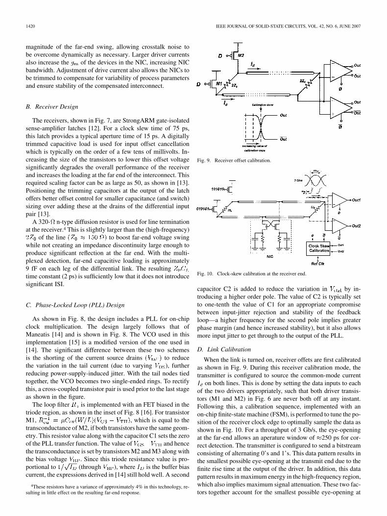
B. Receiver Design
The receivers, shown in Fig. 7, are StrongARM gate-isolatedsense-amplifier latches [12]. For a clock slew time of 75 ps,this latch provides a typical aperture time of 15 ps. A digitallytrimmed capacitive load is used for input offset cancellationwhich is typically on the order of a few tens of millivolts. In-creasing the size of the transistors to lower this offset voltagesignificantly degrades the overall performance of the receiverand increases the loading at the far end of the interconnect. Thisrequired scaling factor can be as large as 50, as shown in [13].Positioning the trimming capacitors at the output of the latchoffers better offset control for smaller capacitance (and switch)sizing over adding these at the drains of the differential inputpair [13].
A 320- n-type diffusion resistor is used for line terminationat the receiver.4 This is slightly larger than the (high-frequency)
of the line to boost far-end voltage swingwhile not creating an impedance discontinuity large enough toproduce significant reflection at the far end. With the multi-plexed detection, far-end capacitive loading is approximately9 fF on each leg of the differential link. The resultingtime constant (2 ps) is sufficiently low that it does not introducesignificant ISI.
C. Phase-Locked Loop (PLL) Design
As shown in Fig. 8, the design includes a PLL for on-chipclock multiplication. The design largely follows that ofManeatis [14] and is shown in Fig. 8. The VCO used in thisimplementation [15] is a modified version of the one used in[14]. The significant difference between these two schemesis the shorting of the current source drains to reducethe variation in the tail current (due to varying ), furtherreducing power-supply-induced jitter. With the tail nodes tiedtogether, the VCO becomes two single-ended rings. To rectifythis, a cross-coupled transistor pair is used prior to the last stageas shown in the figure.
The loop filter is implemented with an FET biased in thetriode region, as shown in the inset of Fig. 8 [16]. For transistorM1, , which is equal to thetransconductance of M2, if both transistors have the same geom-etry. This resistor value along with the capacitor C1 sets the zeroof the PLL transfer function. The value of and hencethe transconductance is set by transistors M2 and M3 along withthe bias voltage . Since this triode resistance value is pro-portional to (through ), where is the buffer biascurrent, the expressions derived in [14] still hold well. A second
4These resistors have a variance of approximately 4% in this technology, re-sulting in little effect on the resulting far-end response.
Fig. 9. Receiver offset calibration.
Fig. 10. Clock-skew calibration at the receiver end.
capacitor C2 is added to reduce the variation in by in-troducing a higher order pole. The value of C2 is typically setto one-tenth the value of C1 for an appropriate compromisebetween input-jitter rejection and stability of the feedbackloop—a higher frequency for the second pole implies greaterphase margin (and hence increased stability), but it also allowsmore input jitter to get through to the output of the PLL.
D. Link Calibration
When the link is turned on, receiver offets are first calibratedas shown in Fig. 9. During this receiver calibration mode, thetransmitter is configured to source the common-mode current
on both lines. This is done by setting the data inputs to eachof the two drivers appropriately, such that both driver transis-tors (M1 and M2) in Fig. 6 are never both off at any instant.Following this, a calibration sequence, implemented with anon-chip finite-state machine (FSM), is performed to tune the po-sition of the receiver clock edge to optimally sample the data asshown in Fig. 10. For a throughput of 3 Gb/s, the eye-openingat the far-end allows an aperature window of 250 ps for cor-rect detection. The transmitter is configured to send a bitstreamconsisting of alternating 0’s and 1’s. This data pattern results inthe smallest possible eye-opening at the transmit end due to thefinite rise time at the output of the driver. In addition, this datapattern results in maximum energy in the high-frequency region,which also implies maximum signal attenuation. These two fac-tors together account for the smallest possible eye-opening at

JOSE AND SHEPARD: DISTRIBUTED LOSS-COMPENSATION TECHNIQUES FOR ENERGY-EFFICIENT LOW-LATENCY ON-CHIP COMMUNICATION 1421
Fig. 11. Skewing/de-skewing circuits.
Fig. 12. Timing diagram.
the receiver end. The clock delay elements consist of inverterstages with digitally trimmed capacitive loading, providing amaximum delay of 250 ps in steps of 8 ps. The calibrationcontroller varies this clock delay from minimum to maximumand vice versa to position the clock edge at the optimal location.
E. Data Skewing and Deskewing
The system is designed to operate with two cycles of la-tency, including data skewing and de-skewing, with a cycletime of 667 ps (1.5 GHz). These skewing (de-skewing) latchesare shown in Fig. 11 with the timing diagram shown in Fig. 12.Bit 0 of the input is latched by the skewing latch at the
rising clock edge (cycle ) followed by bit 1, which is latchedon at the next falling clock edge. Both the bits of the input
are available at the output of the de-skewing latchesafter two clock cycles (cycle ), as shown in Fig. 12. Thedelay of the receiver and transmit clock phases is determinedin the calibration sequence described above. The link latencyis constrained by the synchronization requirement that the sumof the transmitter delay, link latency, and receiver latch delaymust be less than a half a cycle (333 ps). For the system con-sidered here, link latencies up to 270 ps can be accommodated.The 14-mm link considered here has a latency of approximately170 ps.
1422 IEEE JOURNAL OF SOLID-STATE CIRCUITS, VOL. 42, NO. 6, JUNE 2007
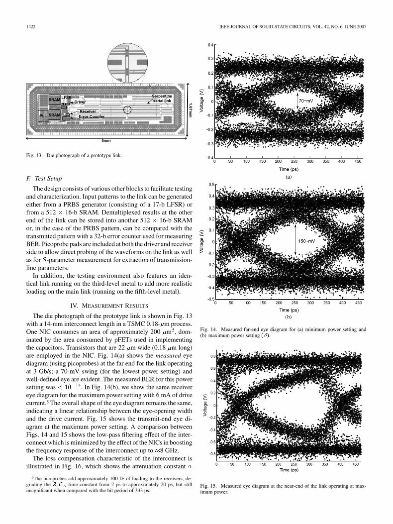
Fig. 13. Die photograph of a prototype link.
F. Test Setup
The design consists of various other blocks to facilitate testingand characterization. Input patterns to the link can be generatedeither from a PRBS generator (consisting of a 17-b LFSR) orfrom a 512 16-b SRAM. Demultiplexed results at the otherend of the link can be stored into another 512 16-b SRAMor, in the case of the PRBS pattern, can be compared with thetransmitted pattern with a 32-b error counter used for measuringBER. Picoprobe pads are included at both the driver and receiverside to allow direct probing of the waveforms on the link as wellas for -parameter measurement for extraction of transmission-line parameters.
In addition, the testing environment also features an iden-tical link running on the third-level metal to add more realisticloading on the main link (running on the fifth-level metal).
IV. MEASUREMENT RESULTS
The die photograph of the prototype link is shown in Fig. 13with a 14-mm interconnect length in a TSMC 0.18- m process.One NIC consumes an area of approximately 200 m , dom-inated by the area consumed by pFETs used in implementingthe capacitors. Transistors that are 22 m wide (0.18 m long)are employed in the NIC. Fig. 14(a) shows the measured eyediagram (using picoprobes) at the far end for the link operatingat 3 Gb/s; a 70-mV swing (for the lowest power setting) andwell-defined eye are evident. The measured BER for this powersetting was . In Fig. 14(b), we show the same receivereye diagram for the maximum power setting with 6 mA of drivecurrent.5 The overall shape of the eye diagram remains the same,indicating a linear relationship between the eye-opening widthand the drive current. Fig. 15 shows the transmit-end eye di-agram at the maximum power setting. A comparison betweenFigs. 14 and 15 shows the low-pass filtering effect of the inter-connect which is minimized by the effect of the NICs in boostingthe frequency response of the interconnect up to 8 GHz.
The loss compensation characteristic of the interconnect isillustrated in Fig. 16, which shows the attenuation constant
5The picoprobes add approximately 100 fF of loading to the receivers, de-grading the Z C time constant from 2 ps to approximately 20 ps, but stillinsignificant when compared with the bit period of 333 ps.
Fig. 14. Measured far-end eye diagram for (a) minimum power setting and(b) maximum power setting (�).
Fig. 15. Measured eye diagram at the near-end of the link operating at max-imum power.

JOSE AND SHEPARD: DISTRIBUTED LOSS-COMPENSATION TECHNIQUES FOR ENERGY-EFFICIENT LOW-LATENCY ON-CHIP COMMUNICATION 1423
Fig. 16. (a) Measured attenuation constant (�) and (b) measured phase con-stant (�) as a function of frequency.
for the 14-mm interconnect as extracted from the measured-parameters with and without enabled NICs; the NICs, when
enabled, reduce by approximately 0.9 dB/mm at 3 GHz.Inactive NICs add approximately 40 fF of loading (primarilygate capacitance) to the interconnect every two millimeters;this additional loading only increases by approximately0.1 dB/mm (at 3 GHz) compared with a wire with no NICs atall. Also shown in the same figure is the phase velocity of theinterconnect, which clearly shows the tradeoff between losscompensation and latency—lower attenuation implies higherlatency. The measured latency of the 14-mm link, determinedthrough probing, is 10.7 ps/mm with the NICs present butunbiased and 12.1 ps/mm with the NICs biased on. The latencyof the link in the absence of any NIC loading would be approx-imately 8 ps/mm. This compares with a latency of more than18.6 ps/mm for an identical optimally buffered link.
The link, through the action of the drivers, consumes ap-proximately 2 pJ/b, which is consistent with the predictions ofFig. 1(a). This includes the power consumed in the NICs as
TABLE ISUMMARY OF CHARACTERISTICS AND MEASURED PERFORMANCE
well as the predrivers.6 The use of DDR allows serialization tobe performed with the limited power overhead of skewing andde-skewing latches. Table I summarizes the measured resultsand performance characteristics. Simulated comparison numberfor the energy per bit and latency of the optimally repeated linkare indicated, which are consistent with the values of Fig. 1.
V. CONCLUSION
We have demonstrated the use of NICs to compensate fortransmission-line losses in on-chip global interconnects. Incontrast to repeaterless implementations, the use of NICs (asshunt “repeaters”) improves bandwidth at a latency cost. Theresulting latencies are still significantly lower than conventionaloptimally buffered links. Bit energies are also substantiallyless (factor-of-three) for line-widths m as comparedwith optimally buffered RC lines. Bit energies can be furtherimproved by running the link at higher bit rates as most of thepower dissipation is static. Higher bandwidth copper wires indeep-submicrometer technologies will allow the advantagesof distributed loss compensation to be achieved with narrowerwires, resulting in a 33% increase [2] in the bandwidth density.
REFERENCES
[1] C. Kim, D. Burger, and S. W. Keckler, “Nonuniform cache architec-tures for wire-delay dominated on-chip caches,” IEEE Micro, no. 6, pp.99–107, Nov.–Dec. 2003.
[2] R. Ho, K. W. Mai, and M. A. Horowitz, “The future of wires,” Proc.IEEE, vol. 89, no. 4, pp. 490–504, Apr. 2001.
[3] P. Saxena, N. Menezes, P. Cocchini, and D. A. Kirkpatrick, “Repeaterscaling and its impact on CAD,” IEEE Trans. Comput.-Aided Des. In-tegr. Circuits Syst., vol. 23, no. 4, pp. 451–463, Apr. 2004.
[4] A. P. Jose, G. Patounakis, and K. L. Shepard, “Pulsed current-modesignaling for nearly speed-of-light intrachip communication,” IEEE J.Solid-State Circuits, vol. 41, no. 4, pp. 772–780, Apr. 2006.
6The power consumed in the PLL is not included in this energy-per-bit figureas this is not an overhead of the link itself.

1424 IEEE JOURNAL OF SOLID-STATE CIRCUITS, VOL. 42, NO. 6, JUNE 2007
[5] A. Jose and K. L. Shepard, “Distributed loss compensation for low-latency on-chip interconnects,” in Proc. IEEE Int. Solid-State CircuitsConf., 2006, pp. 19–20.
[6] J. G. Linvill, “Transistor negative impedance converters,” Proc. IRE,vol. 41, pp. 725–729, Jun. 1953.
[7] H.-T. Ahn and D. J. Allstot, “A 0.5–8.5 GHz differential CMOS dis-tributed amplifier,” IEEE J. Solid-State Circuits, vol. 37, no. 8, pp.985–993, Aug. 2002.
[8] F. O’Mahony, C. P. Yue, M. A. Horowitz, and S. S. Wong, “A 10-GHzglobal clock distribution using coupled standing-wave oscillators,”IEEE J. Solid-State Circuits, vol. 38, no. 11, pp. 1813–1820, Nov.2003.
[9] Low Voltage Differential Signals (LVDS) for Scalable Coherent Inter-face (SCI), IEEE Std. 1596.3-1196, 1994.
[10] S. Galal and B. Razavi, “10-Gb/s limiting amplifier and laser/modu-lator driver in 0.18- �m CMOS technology,” IEEE J. Solid-State Cir-cuits, vol. 38, no. 12, pp. 2138–2146, Dec. 2003.
[11] D. M. Pozar, Microwave Engineering, 2nd ed. New York: Wiley,1999.
[12] J. Montanaro et al., “A 160-MHz, 32-b, 0.5-W CMOS RISC micropro-cessor,” IEEE J. Solid-State Circuits, vol. 31, no. 11, pp. 1703–1712,Nov. 1996.
[13] M.-J. E. Lee, W. J. Dally, and P. Chiang, “Low-power area-efficienthigh-speed I/O circuit techniques,” IEEE J. Solid-State Circuits, vol.35, no. 11, pp. 1591–1599, Nov. 2000.
[14] J. G. Maneatis, “Low-jitter process-independent DLL and PLL basedon self-biased techniques,” IEEE J. Solid-State Circuits, vol. 31, no.11, pp. 1723–1732, 1996.
[15] J. G. Maneatis, J. Kim, I. McClatchie, J. Maxey, and M. Shankaradas,“Self-biased high-bandwidth low-jitter 1-to-4096 multiplier clockgenerator PLL,” IEEE J. Solid-State Circuits, vol. 38, no. 11, pp.1795–1803, Nov. 2003.
[16] B. Razavi, “A 2.4-GHz CMOS receiver for IEEE 802.11 wirelessLANs,” IEEE J. Solid-State Circuits, vol. 34, no. 10, pp. 1382–1385,Oct. 1999.
Anup P. Jose (S’01–M’06) received the B.Tech. de-gree from the Indian Institute of Technology, Madras,India, in 2001, and the M.S. and Ph.D. degrees fromColumbia University, New York, NY, in 2003 and2006, respectively, all in electrical engineering. Hisresearch focused on low-latency low-power intercon-nects for on-chip networks.
He was with the IBM T. J. Watson ResearchCenter, Yorktown Heights, NY, for the summers of2002–2004, where he was involved with on-chipjitter measurement circuits and an on-chip spectrum
analyzer. During the summer of 2005, he was with the IBM Austin ResearchLaboratory, Austin, TX, where he was responsible for the design of on-chipsampling circuits in 65-nm technology. He is currently a Senior DesignEngineer with the high-speed I/O group at AMD’s Boston Design Center,Boxborough, MA.
Dr. Jose was the recipient of the 2005 Best Paper Award at the EuropeanSolid-State Circuits Conference.
Kenneth L. Shepard (S’85–M’92–SM’03) re-ceived the B.S.E. degree from Princeton University,Princeton, NJ, in 1987 and the M.S. and Ph.D.degrees in electrical engineering from StanfordUniversity, Stanford, CA, in 1988 and 1992, respec-tively.
From 1992 to 1997, he was a Research StaffMember and Manager with the VLSI Design De-partment, the IBM T. J. Watson Research Center,Yorktown Heights, NY, where he was responsiblefor the design methodology for IBM’s G4 S/390
microprocessors. Since 1997, he has been with Columbia University, wherehe is now Associate Professor. He also served as Chief Technology Officer ofCadMOS Design Technology, San Jose, CA, until its acquisition by CadenceDesign Systems in 2001. His current research interests include design toolsfor advanced CMOS technology, on-chip test and measurement circuitry,low-power design techniques for digital signal processing, low-power intrachipcommunications, and CMOS imaging applied to biological applications.
Dr. Shepard was the recipient of the Fannie and John Hertz Foundation Doc-toral Thesis Prize in 1992. At IBM, he was the recipient of Research DivisionAwards in 1995 and 1997. He was also the recipient of a National ScienceFoundation CAREER Award in 1998 and IBM University Partnership Awardsfrom 1998 through 2002. He was also awarded the 1999 Distinguished Fac-ulty Teaching Award from the Columbia Engineering School Alumni Asso-ciation. He has been an Associate Editor of IEEE TRANSACTIONS ON VERY
LARGE SCALE INTEGRATION (VLSI) SYSTEMS and was the Technical ProgramChair and General Chair for the 2002 and 2003 International Conference onComputer Design, respectively. He has served on the program committees forISSCC, VLSI Symposium, ICCAD, DAC, ISCAS, ISQED, GLS-VLSI, TAU,and ICCD.