distributed modeling of 4-port transistor for linear mmw ... · approach enables to determine a...
TRANSCRIPT
Distributed modeling of 4-port transistor for linear mmW designapplication
Wafa Khelifi∗, Tibault Reveyrand∗, Julien Lintignat∗, Bernard Jarry∗, Raymond Quere∗, Luc Lapierre†,Vincent Armengaud†
∗XLIM, 123 av. Albert Thomas, 87060 Limoges Cedex, France†CNES, 18 av. E. Belin, 31400 Toulouse, France
Abstract—This paper presents an approach for the distributedmodeling of a 4-port transistor. The proposed principle relieson considering any multi-finger transistor as the association ofa number of elementary active linked together with extrinsicpassive networks. An electromagnetic analysis allows to set theelectrical equivalent scheme of the passive networks whereas theinternal active device is defined by an equivalent model. It isshown how the equivalent intrinsic device (based on 2 fingers) andthe values of the suitably defined distributed parasitic networkelements can be accurately extracted and modeled on the basisof standard measurements. This approach is validated by thecomparison of measured and simulated results for a GaAs HEMTtransistor in the Ku-band.
Index Terms—Electromagnetic analysis, GaAs HEMT, S-parameters, characterization, modeling.
I. INTRODUCTION
The development of high-performance microwave and
MMIC circuits requires accurate computer aided design
(CAD) tools in the design phase [1]. Indeed, the success of
the design usually relies on the quality of non-linear transistor
model. In this context, accurate electrical device model that
describes the operation up to millimeter-wave frequencies is a
key aspect.
Conventional scalable models, provided within Process De-
sign Kits (PDKs), are based on equivalent circuits whose
parameters are scaled with device size and finger number
[2]. Some of these approaches may not be sufficient when
operating at high frequencies. Indeed, a large number of
measurements must be made on different device structures in
order to obtain a good evolutionary model. However, special
attention to extrinsic networks modeling and identification
should be given.
Furthermore, the distributed effects, which occurs at very
high frequencies, can greatly reduce the performance of the
transistor. Such behavior is not easy to identify by a simple
extrinsic network [3]. Distributed effects must be taken into
account in the modeling phase of the device or even more
complicated equivalent circuit structures must be evaluated [4].
For this problem, some distributed and semi-distributed models
have been proposed. Those models are based on electromag-
netic simulations (EM) and S-parameters measurements [5],
[6]. Although this model is capable of accurate small-signal
prediction in 2-ports, it does not present any information on
the performance of the transistor when it is used in 3 or 4-ports
configuration. The novelty of this work lies in the development
of a 4-ports distributed model. Indeed, the accuracy of this
model is illustrated for different transistor configurations:
• 3-ports model with open on one of the source port ;
• 2-ports with two VIA (2 source port are shorted with VIA
holes) ;
• 2-ports featuring with unique VIA (one source port is in
open and the other one is shorted).
The presented modeling approach has been validated up to
40 GHz for GaAs HEMT from UMS foundry. The accuracy of
this approach is highlighted by simulation and measurements
comparisons.
II. PRINCIPLE OF MODELING
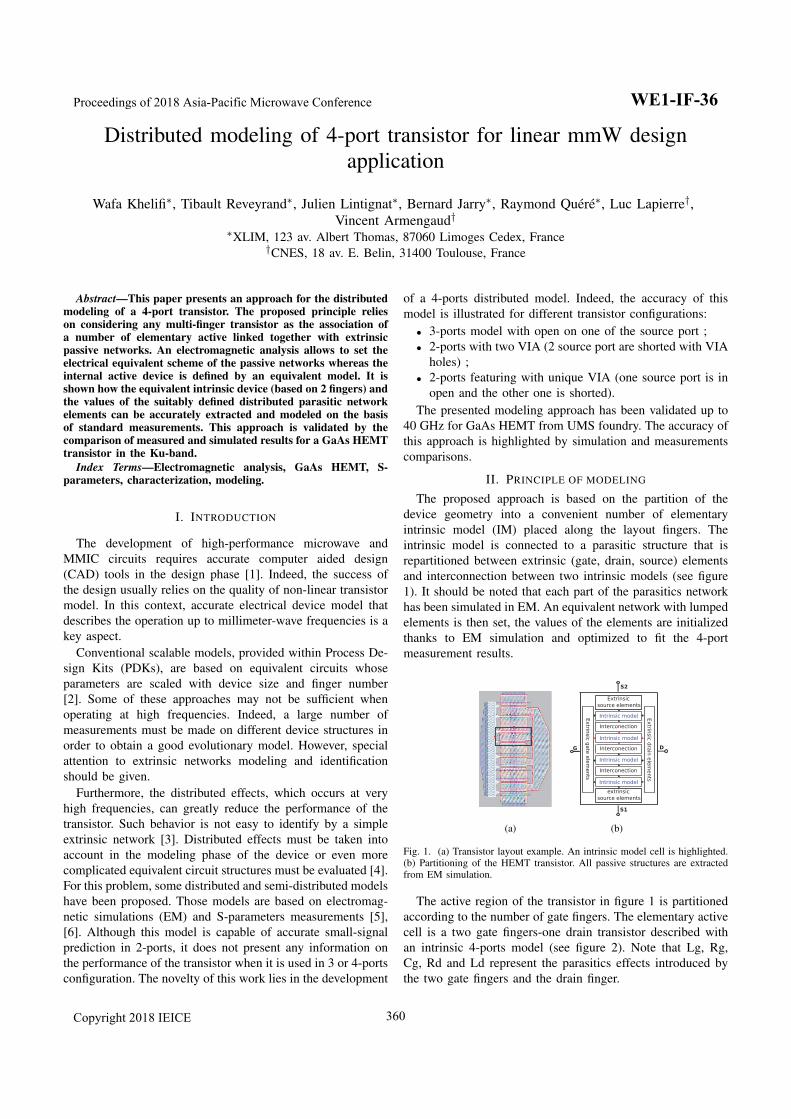
The proposed approach is based on the partition of the
device geometry into a convenient number of elementary
intrinsic model (IM) placed along the layout fingers. The
intrinsic model is connected to a parasitic structure that is
repartitioned between extrinsic (gate, drain, source) elements
and interconnection between two intrinsic models (see figure
1). It should be noted that each part of the parasitics network
has been simulated in EM. An equivalent network with lumped
elements is then set, the values of the elements are initialized
thanks to EM simulation and optimized to fit the 4-port
measurement results.
(a)
Extrinsic source elements
extrinsic source elements
Intrinsic model
Interconection
Intrinsic model
Interconection
Intrinsic model
Interconection
Intrinsic model
Extrinsic gate elements
Extrinsic drain elements
G D
S2
S1
(b)
Fig. 1. (a) Transistor layout example. An intrinsic model cell is highlighted.(b) Partitioning of the HEMT transistor. All passive structures are extractedfrom EM simulation.
The active region of the transistor in figure 1 is partitioned
according to the number of gate fingers. The elementary active
cell is a two gate fingers-one drain transistor described with
an intrinsic 4-ports model (see figure 2). Note that Lg, Rg,
Cg, Rd and Ld represent the parasitics effects introduced by
the two gate fingers and the drain finger.
Proceedings of 2018 Asia-Pacific Microwave Conference
Copyright 2018 IEICE
WE1-IF-36
360
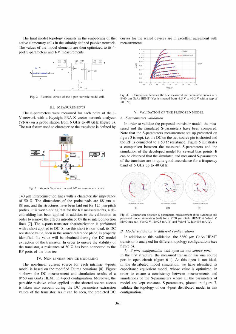
The final model topology consists in the embedding of the
active elementary cells in the suitably defined passive network.
The values of the model elements are then optimized to fit 4-
port S-parameters and I-V measurements.
Cgd
Cgs
Rgd
RiCds
RsLs1 Ls2
Lg Rg
Cg
Rd Ld
Vgs
Ls
Ids
Intrinsic model
IM
A B
C D
A B
C
D
Gd
Fig. 2. Electrical circuit of the 4-port intrinsic model cell.
III. MEASUREMENTS
The S-parameters were measured for each point of the I-
V network with a Keysight PNA-X vector network analyzer
(VNA) on a probe station from 6 GHz to 40 GHz (figure 3).
The test fixture used to characterize the transistor is defined by
R_DC
R_DC
Vds
PNA-X
1 2 3
Vgs
G D
S1
S2
4
Short
Short
Fig. 3. 4-ports S-parameters and I-V measurements bench.
140 μm interconnection lines with a characteristic impedance
of 50 Ω. The dimensions of the probe pads are 88 μm ×88 μm, and the structures have been laid out for 125 μm-pitch
probes. It is worth-noting that for the RF measurements, a de-
embedding has been applied in addition to the calibration in
order to remove the effects introduced by these interconnection
lines [7]. The 4-ports transistor characterization is performed
with a short applied to DC. Since this short is non-ideal, its DC
resistance value, seen in the source reference plane, is properly
identified. Its value will be obtained during the DC model
extraction of the transistor. In order to ensure the stability of
the transistor, a resistance of 50 Ω has been connected to the
RF ports of the bias tee.
IV. NON-LINEAR DEVICE MODELING
The non-linear current source for each intrinsic 4-ports
model is based on the modified Tajima equations [8]. Figure
4 shows the DC measurement and simulation results of a
8*60 μm GaAs HEMT in 4-port configuration. Moreover, the
parasitic resistive value applied to the shorted source access
is taken into account during the DC parameters extraction
values of the transistor. As it can be seen, the predicted DC
curves for the scaled devices are in excellent agreement with
measurements.
Measurement
Model
Vgs(V)
Fig. 4. Comparison between the I-V measured and simulated curves of a8*60 μm GaAs HEMT (Vgs is stepped from -1.5 V to +0.2 V with a step of+0.1 V).
V. VALIDATION OF THE PROPOSED MODEL
A. S-parameters validationIn order to validate the proposed transistor model, the mea-
sured and the simulated S-parameters have been compared.
Note that the S-parameters measurement set up presented on
figure 3 is kept, i.e. the DC on the two source pin is shorted and
the RF is connected to a 50 Ω resistance. Figure 5 illustrates
a comparison between the measured S-parameters and the
simulation of the developed model for several bias points. It
can be observed that the simulated and measured S-parameters
of the transistor are in quite good accordance for a frequency
band of 6 GHz up to 40 GHz.
(a) (b) (c)
Fig. 5. Comparison between S-parameters measurement (blue symbols) andproposed model simulation (red) for a 8*60 μm GaAs HEMT at Vds=0 V,Ids=0 mA (a); Vds=2 V, Ids=23 mA (b) and Vds=1 V, Ids=119 mA (c).
B. Model validation in different configurationsIn addition to this validation, the 8*60 μm GaAs HEMT
transistor is analyzed for different topology configurations (see
figure 6).1) 3-port configuration with open on one source port:
In the first structure, the measured transistor has one source
port in open circuit (figure 6-1). As this open is not ideal,
in the distributed model simulation, we have identified its
capacitance equivalent model, whose value is optimized, in
order to ensure a consistency between measurements and
simulations of the S-parameters where all the parameters of
model are kept constant. S-parameters, plotted in figure 7,
validate the topology of our 4-port distributed model in this
configuration.
361
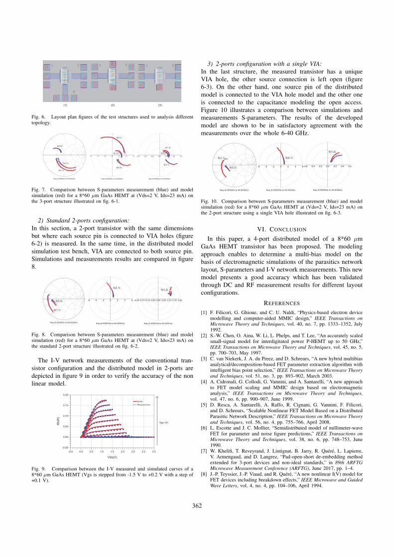
Fig. 6. Layout plan figures of the test structures used to analysis differenttopology.
Fig. 7. Comparison between S-parameters measurement (blue) and modelsimulation (red) for a 8*60 μm GaAs HEMT at (Vds=2 V, Ids=23 mA) onthe 3-port structure illustrated on fig. 6-1.
2) Standard 2-ports configuration:In this section, a 2-port transistor with the same dimensions
but where each source pin is connected to VIA holes (figure
6-2) is measured. In the same time, in the distributed model
simulation test bench, VIA are connected to both source pin.
Simulations and measurements results are compared in figure
8.
Fig. 8. Comparison between S-parameters measurement (blue) and modelsimulation (red) for a 8*60 μm GaAs HEMT at (Vds=2 V, Ids=23 mA) onthe standard 2-port structure illustrated on fig. 6-2.
The I-V network measurements of the conventional tran-
sistor configuration and the distributed model in 2-ports are
depicted in figure 9 in order to verify the accuracy of the non
linear model.
0.0 0.5 1.0 1.5 2.0 2.5 3.0-0.5 3.5
0.00
0.05
0.10
0.15
-0.05
0.20
Vds(V)
Ids(A)
ModelMeasurement
Vgs (V)
Fig. 9. Comparison between the I-V measured and simulated curves of a8*60 μm GaAs HEMT (Vgs is stepped from -1.5 V to +0.2 V with a step of+0.1 V).
3) 2-ports configuration with a single VIA:In the last structure, the measured transistor has a unique
VIA hole, the other source connection is left open (figure
6-3). On the other hand, one source pin of the distributed
model is connected to the VIA hole model and the other one
is connected to the capacitance modeling the open access.
Figure 10 illustrates a comparison between simulations and
measurements S-parameters. The results of the developed
model are shown to be in satisfactory agreement with the
measurements over the whole 6-40 GHz.
Fig. 10. Comparison between S-parameters measurement (blue) and modelsimulation (red) for a 8*60 μm GaAs HEMT at (Vds=2 V, Ids=23 mA) onthe 2-port structure using a single VIA hole illustrated on fig. 6-3.
VI. CONCLUSION
In this paper, a 4-port distributed model of a 8*60 μm
GaAs HEMT transistor has been proposed. The modeling
approach enables to determine a multi-bias model on the
basis of electromagnetic simulations of the parasitics network
layout, S-parameters and I-V network measurements. This new
model presents a good accuracy which has been validated
through DC and RF measurement results for different layout
configurations.
REFERENCES
[1] F. Filicori, G. Ghione, and C. U. Naldi, “Physics-based electron devicemodelling and computer-aided MMIC design,” IEEE Transactions onMicrowave Theory and Techniques, vol. 40, no. 7, pp. 1333–1352, July1992.
[2] S.-W. Chen, O. Aina, W. Li, L. Phelps, and T. Lee, “An accurately scaledsmall-signal model for interdigitated power P-HEMT up to 50 GHz,”IEEE Transactions on Microwave Theory and Techniques, vol. 45, no. 5,pp. 700–703, May 1997.
[3] C. van Niekerk, J. A. du Preez, and D. Schreurs, “A new hybrid multibiasanalytical/decomposition-based FET parameter extraction algorithm withintelligent bias point selection,” IEEE Transactions on Microwave Theoryand Techniques, vol. 51, no. 3, pp. 893–902, March 2003.
[4] A. Cidronali, G. Collodi, G. Vannini, and A. Santarelli, “A new approachto FET model scaling and MMIC design based on electromagneticanalysis,” IEEE Transactions on Microwave Theory and Techniques,vol. 47, no. 6, pp. 900–907, June 1999.
[5] D. Resca, A. Santarelli, A. Raffo, R. Cignani, G. Vannini, F. Filicori,and D. Schreurs, “Scalable Nonlinear FET Model Based on a DistributedParasitic Network Description,” IEEE Transactions on Microwave Theoryand Techniques, vol. 56, no. 4, pp. 755–766, April 2008.
[6] L. Escotte and J. C. Mollier, “Semidistributed model of millimeter-waveFET for parameter and noise figure predictions,” IEEE Transactions onMicrowave Theory and Techniques, vol. 38, no. 6, pp. 748–753, June1990.
[7] W. Khelifi, T. Reveyrand, J. Lintignat, B. Jarry, R. Quere, L. Lapierre,V. Armengaud, and D. Langrez, “Pad-open-short de-embedding methodextended for 3-port devices and non-ideal standards,” in 89th ARFTGMicrowave Measurement Conference (ARFTG), June 2017, pp. 1–4.
[8] J.-P. Teyssier, J.-P. Viaud, and R. Quere, “A new nonlinear I(V) model forFET devices including breakdown effects,” IEEE Microwave and GuidedWave Letters, vol. 4, no. 4, pp. 104–106, April 1994.
362