dlc display co., limiteditem contents unit size 5.7 inch resolution 640(rgb) x 480 / technology type...
TRANSCRIPT

DLC Display Co., Limited
德爾西顯示器有限公司
MODEL No:DLC0570GMG
TEL: 86-755-86029824
FAX: 86-755-86029827
E-MAIL: [email protected]
WEB: www.dlcdisplay.com

Module Name: DLC0570GMG Ver1.1
http://www.dlcdisplay.com Email:[email protected] 2 of 17
.
Record of Revision
Date Revision No. Summary
2010-03-04 1.0 Rev 1.0 was issued2015-07-07 1.1 Update Operating Temperature

Module Name: DLC0570GMG Ver1.1
http://www.dlcdisplay.com Email:[email protected] 3 of 17
1. ScopeThis data sheet is to introduce the specification of DLC0570GMG active matrix TFT module. It iscomposed of a color TFT-LCD panel, driver ICs, FPC and a backlight unit. The 5.7′′ display areacontains 640(RGB) x 480 pixels.
2. ApplicationDigital equipments which need color display, POS, mobile navigator/video systems.
3. General Information
Item Contents Unit
Size 5.7 inch
Resolution 640(RGB) x 480 /
Technology type a-si TFT /
Interface TTL
Color depth 262K
Pixel pitch 0.180x0.180 mm
Pixel Configuration R.G.B. Vertical Stripe
Outline Dimension (W x H x D) 144.00x 104.60x12.30 mm
Active Area 115.20 x 86.40 mm
Display ModeTransmissive,Normally White
/
Viewing Direction 6 O’clock /
Backlight Type LEDs /

Module Name: DLC0570GMG Ver1.1
http://www.dlcdisplay.com Email:[email protected] 4 of 17
4. Outline Drawing

Module Name: DLC0570GMG Ver1.1
http://www.dlcdisplay.com Email:[email protected] 5 of 17
5. Interface signals5.1 CN1 pin assignment
No Symbol I/O Description Remarks1 GND P Ground2 CK I Dot clock. Latch data at falling edge of CK.
3 Hsync I Horizontal sync signal in SYNC mode. Pull low orfloating when DE mode.
4 Vsync I Vertical sync signal in SYNC mode. Pull low orfloating when DE mode.
5 GND P Ground6 R0 I Red data (LSB)7 R1 I Red data8 R2 I Red data9 R3 I Red data10 R4 I Red data11 R5 I Red data (MSB)12 GND P Ground13 G0 I Green data(LSB)14 G1 I Green data15 G2 I Green data16 G3 I Green data17 G4 I Green data18 G5 I Green data(MSB)19 GND P Ground20 B0 I Blue data(LSB)21 B1 I Blue data22 B2 I Blue data23 B3 I Blue data24 B4 I Blue data25 B5 I Blue data(MSB)26 GND P Ground
27 ENAB I Data enable signal in DE mode. This pin mustpull high when SYNC mode.
28 VCC P Power supply29 VCC P Power supply
30 R/L I Set horizontal scan direction: Low/NC: left toright; High: right to left
31 U/D I Set vertical scan direction: High/NC: up todown; Low: down to up
32 NC - No connection33 GND P Ground

Module Name: DLC0570GMG Ver1.1
http://www.dlcdisplay.com Email:[email protected] 6 of 17
5.2 CN2 pin assignment (Backlight interface)
No Symbol I/O Description Comment1 AN1 P LED Anode Terminal Red2 AN2 P LED Anode Terminal Red3 AN3 P LED Anode Terminal Red4 CA1 P LED Cathode Terminal White5 CA2 P LED Cathode Terminal Blue6 CA3 P LED Cathode Terminal Black
6. Absolute maximum Ratings
6.1.Electrical Absolute max. ratings
Parameter Symbol MIN MAX Unit Remark
Power Voltage VCC -0.5 5.0 V
Input voltageR0~R5, G0~G5, B0~B5, CK, Hsync,
Vsync, Enable, R/L, U/D-0.5 5.0 V
6.2 Environment Conditions
Item Symbol MIN MAX Unit Remark
Operating Temperature TOPR -20 70 ℃
Storage Temperature TSTG -30 85 ℃

Module Name: DLC0570GMG Ver1.1
http://www.dlcdisplay.com Email:[email protected] 7 of 17
7. Electrical Specifications
7.1 Electrical characteristicsGND=0V, Ta=25℃
Item Symbol MIN TYP MAX Unit Remark
Supply Voltage VCC 3.0 3.3 3.6 V
Permissive input ripplevoltage
Vr - - 100 mVp-p VCC =3.3V
Input Signal Voltage
VIL 0 - 0.3*VCC V
VIH 0.7* IOVCC - VCC V
7.2 LED Backlight Ta=25℃
Item Symbol MIN TYP MAX Unit Remark
Series 1 Forward Current I1 - 25 - mA
For each oneSeries 2 Forward Current I2 - 25 -- mA
Series 3 Forward Current I3 - 25 mA
Forward Voltage VF 19.95 - 25.9 V
Backlight power WBL 1732.5 mW Note
Life time 25,000 50,000 Hrs
Note: Operating life means brightness goes down to 50% initial brightness.Typical operating life time is estimated data.
LED connection of backlight
Module Name: DLC0570GMG Ver1.1
http://www.dlcdisplay.com Email:[email protected] 8 of 17
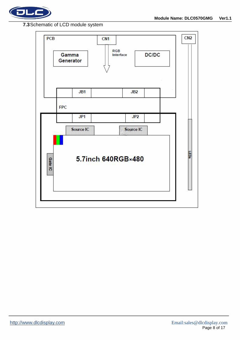
7.3Schematic of LCD module system

Module Name: DLC0570GMG Ver1.1
http://www.dlcdisplay.com Email:[email protected] 9 of 17
8. Command/AC Timing8.1SYNC mode
Parameter Symbol Symbol Min Typ Max Unit
CKDotclk frequency Fclk 24.8 25.2 34.2 MHz
Dotclk cycle Tclk 29.24 39.68 40.32 ns
Hsync
Horizontal display area Thd 640 640 640 Tclk
1 horizontal line Th 800 800 1000 Tclk
Hsync pulse width Thpw 1 - - Tclk
Horizontal blank Thb 144 144 144 Tclk
Horizontal front porch Thfp 16 16 216 Tclk
Vsync
Frame rate - - 60 - Hz
Vertical display area Tvd 480 480 480 Th
Vsync period time Tv 516 525 570 Th
Vsync pulse width Tvpw 1 - - Th
Vsync blank Tvb 35 35 35 Th
Vsync front porch Tvfp 1 10 55 Th
8.2 DE mode
Description Symbol Min Typ Max Unit
CK Dot clock frequency Fclk 24.8 25.2 34.2 MHz
Horizontalsection
Horizontal total Th 800 800 1000 Tclk
H Total blank Thb+Thfp 160 160 360 Tclk
Valid Data Width Thd 640 640 640 Tclk
Verticalsection
Frame rate - - 60 - Hz
Vertical total Tv 516 525 570 Th
V total blank Tvb+Tvfp 36 45 90 Th
Valid Data Width Tvd 480 480 480 Th
Note: The LCM could auto-detect which mode is working.

Module Name: DLC0570GMG Ver1.1
http://www.dlcdisplay.com Email:[email protected] 10 of 17
8.3Timing diagram
8.3.1 vertical input timing
8.3.2 Horizontal Input Timing

Module Name: DLC0570GMG Ver1.1
http://www.dlcdisplay.com Email:[email protected] 11 of 17
8.4 AC input characteristics
Parameter Symbol Min Typ Max Unit Conditions
CK pulse duty Tcwh 40% 50% 60% Tclk
Vsync setup time Tvst 8 - - ns
Vsync hold time Tvhd 8 - - ns
Hsync setup time Thst 8 - - ns
Hsync hold time Thhd 8 - - ns
Data setup time Tdsu 8 - - ns Rn, Gn, Bn to Dotclk
Data hold time Tdhd 8 - - ns Rn, Gn, Bn to Dotclk
ENAB setup time Tesu 8 ns
AC input characteristics

Module Name: DLC0570GMG Ver1.1
http://www.dlcdisplay.com Email:[email protected] 12 of 17
8.5 POWER ON/OFF SEQUENCE
Item Symbol Min Typ Max Unit Remark
VCC 3.0V to signal starting Tp1 5 - 50 ms
Signal starting to backlight on Tp2 50 - - ms
Signal off to VCC 3.0V Tp3 0 - 50 ms
Backlight off to signal off Tp4 50 - - ms

Module Name: DLC0570GMG Ver1.1
http://www.dlcdisplay.com Email:[email protected] 13 of 17
9 Optical Specification
Item Symbol Condition Min Typ. Max. Unit Remark
Contrast Ratio CR θ=0° 400 500 -Note1Note2
Response Time Ton/ Toff 25℃ - 40 - msNote1Note3
View Angles
ΘT
CR≧10
60 70 -
Degree Note 4ΘB 50 60 -
ΘL 60 70 -
θR 60 70 -
Chromaticity
Whitex
Brightnessis on Typ-0.05
0.302
Typ+0.05Note5,Note1
y 0.329
Redx 0.598
y 0.342
Greenx 0.334
y 0.585
Bluex 0.142
y 0.102
NSTC S - 50 % Note 5
Luminance L 320 400 - cd/m2 Note1Note6
Uniformity U 75 80 - %Note1Note7
Note 1: Definition of optical measurement system.
Temperature = 25℃(±3℃)
LED back-light: ON, Environment brightness < 150 lx
Module Name: DLC0570GMG Ver1.1
http://www.dlcdisplay.com Email:[email protected] 14 of 17
Note 2: Contrast ratio is defined as follow:
pixelsblack all with Luminance Surfacepixels whiteall with Luminance Surface=RatioContrast
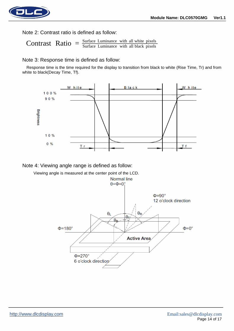
Note 3: Response time is defined as follow:Response time is the time required for the display to transition from black to white (Rise Time, Tr) and from
white to black(Decay Time, Tf).
Note 4: Viewing angle range is defined as follow:Viewing angle is measured at the center point of the LCD.

Module Name: DLC0570GMG Ver1.1
http://www.dlcdisplay.com Email:[email protected] 15 of 17
Note 5: Color chromaticity is defined as follow: (CIE1931)Color coordinates measured at center point of LCD.
100%triangleNTSCofarea
triangleRGBofareaS ´=
Note 6: Luminance is defined as follow:Luminance is defined as the brightness of all pixels “White” at the center of display area on optimum contras
Note 7: Definition of Luminance UniformityActive area is divided into 9 measuring areas (Refer Fig. 2). Every measuring point is placed at thecenter of each measuring area.Luminance Uniformity (U) = Lmin/ LmaxL-------Active area length W----- Active area width

Module Name: DLC0570GMG Ver1.1
http://www.dlcdisplay.com Email:[email protected] 16 of 17
10Environmental / Reliability Tests
No Test Item Condition Judgment criteria
1 High Temp Operation Ts=+70℃, 120hrs Per table in below
2 Low Temp Operation Ta=-20℃, 120hrs Per table in below
3 High Temp Storage Ta=+85℃, 120hrs Per table in below
4 Low Temp Storage Ta=-30℃, 120hrs Per table in below
5 High Temp & HighHumidity Storage
Ta=+40℃, 90% RH120 hours
Per table in below(polarizer discoloration isexcluded)
6 Thermal Shock(Non-operation)
-20℃ 30 min~+70℃ 30 min,Change time:5min, 10 Cycles
Per table in below
7 ESD (Operation)C=150pF, R=330Ω,5points/panelAir:±8KV, 5times;Contact:±4KV, 5 times;
Per table in below
8Vibration(Non-operation)
Frequency range:10~55Hz,Stroke:1.5mmSweep:10Hz~55Hz~10Hz 2 hoursfor each direction of X.Y.Z.
Per table in below
9 Shock(Non-operation)
60G 6ms, ±X,±Y,±Z 3times,for each direction Per table in below
10 PackageDrop Test
Height:80 cm,1 corner, 3 edges, 6 surfaces Per table in below
INSPECTION CRITERION(after test)
Appearance No Crack on the FPC, on the LCD Panel
Alignment of LCD
Panel
No Bubbles in the LCD PanelNo other Defects of Alignment in Active area
Electrical current Within device specifications
Function / Display No Broken Circuit, No Short Circuit or No Black lineNo Other Defects of Display

Module Name: DLC0570GMG Ver1.1
http://www.dlcdisplay.com Email:[email protected] 17 of 17
11Precautions for Use of LCD Modules11.1 Safety
The liquid crystal in the LCD is poisonous. Do not put it in your mouth. If the liquid crystal touches your skin orclothes, wash it off immediately using soap and water.
11.2 HandlingA. The LCD and touch panel is made of plate glass. Do not subject the panel to mechanical shockor to excessive force on its surface.B. Do not handle the product by holding the flexible pattern portion in order to assure thereliabilityC. Transparency is an important factor for the touch panel. Please wear clear finger sacks, glovesand mask to protect the touch panel from finger print or stain and also hold the portionoutside the view area when handling the touch panel.D. Provide a space so that the panel does not come into contact with other components.E. To protect the product from external force, put a covering lens (acrylic board or similar board)and keep an appropriate gap between them.F. Transparent electrodes may be disconnected if the panel is used under environmentalconditions where dew condensation occurs.G. Property of semiconductor devices may be affected when they are exposed to light, possiblyresulting in IC malfunctions.H. To prevent such IC malfunctions, your design and mounting layout shall be done in the waythat the IC is not exposed to light in actual use.
11.3 Static ElectricityA. Ground soldering iron tips, tools and testers when they are in operation.B. Ground your body when handling the products.C. Power on the LCD module before applying the voltage to the input terminals.D. Do not apply voltage which exceeds the absolute maximum rating.E. Store the products in an anti-electrostatic bag or container.
11.4StorageA. Store the products in a dark place at +25℃±10℃ with low humidity (40% RH to 60% RH).Don't expose to sunlight or fluorescent light.B. Storage in a clean environment, free from dust, active gas, and solvent.
11.5 CleaningA. Do not wipe the touch panel with dry cloth, as it may cause scratch.B. Wipe off the stain on the product by using soft cloth moistened with ethanol. Do not allowethanol to get in between the upper film and the bottom glass. It may cause peeling issue ordefective operation. Do not use any organic solvent or detergent other than ethanol.
11.6 Cautions for installing and assemblingBezel edge must be positioned in the area between the Active area and View area. Thebezel may press the touch screen and cause activation if the edge touches the active area.A gap of approximately 0.5mm is needed between the bezel and the top electrode. It maycause unexpected activation if the gap is too narrow. There is a tolerance of 0.2 to 0.3mmfor the outside dimensions of the touch panel and tail. A gap must be made to absorb the
tolerance in the case and connector.