dot character vfd controller/driver · read-enable pin. when this pin is l, data is output to the...
TRANSCRIPT

The information in this document is subject to change without notice. Before using this document, pleaseconfirm that this is the latest version.Not all devices/types available in every country. Please check with local NEC representative foravailability and additional information.
© 1997
MOS INTEGRATED CIRCUIT
µ µ µ µ PD16314
DOT CHARACTER VFD CONTROLLER/DRIVER
DATA SHEET
Document No. S13231EJ1V0DS00 (1st edition)Date Published March 2000 NS CP(K)Printed in Japan
The mark shows major revised point.
DESCRIPTION The µ PD16314 is a VFD controller/driver capable of displaying a dot matrix VFD. It has 80 anode outputs and 24
grid outputs. A single µ PD16314 can display up to 16C x 2L, 20C x 2L, or 24C x 2L. The µ PD16314 has character
generator ROM in which 248 x 5 x 8 dot characters are stored.
FEATURES• Dot matrix VFD controller/driver
• Capable of driving anodes for cursor display (48 units)
• 80 x 8 bits display RAM incorporated
• Capable of alphanumeric and symbolic display through internal ROM (5 by 8 dots)
240 characters plus 8 user-defined characters
• Display contents
16 columns by 2(1) rows + 32(16) cursors, 20 columns by 2(1) rows + 40(20) cursors,
or 24 columns by 2(1) rows + 48(24) cursors.
• Parallel data input/output (switchable between 4 bits and 8 bits) or serial data input/output can be selected.
• On-chip oscillator
• Custom ROM supported
ORDERING INFORMATION
Part Number Package
µ PD16314GJ-001-8EU 144-PIN PLASTIC LQFP(FINE PITCH)(20x20), Standard ROM (ROM code: 001)
µ PD16314GJ-002-8EU 144-PIN PLASTIC LQFP(FINE PITCH)(20x20), Standard ROM (ROM code: 002)
Data S
heet S13231E
J1V0D
S00
2
µ µ µ µ PD
16314
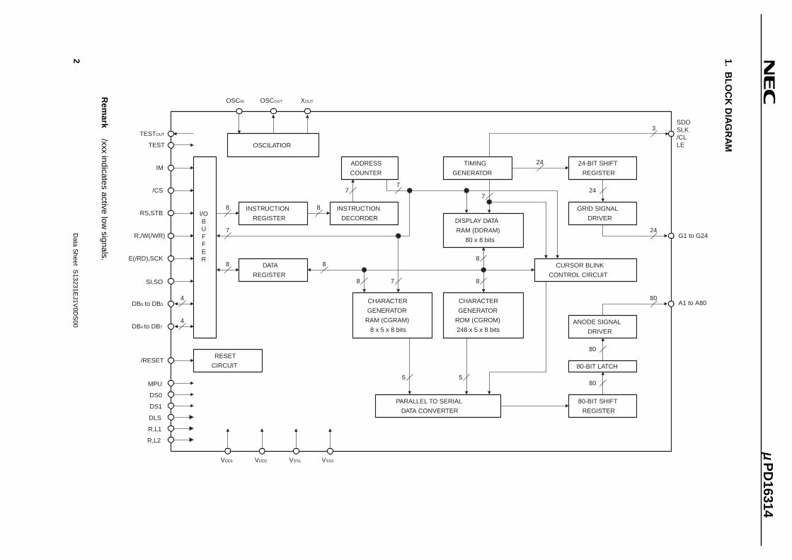
1. BLO
CK
DIA
GR
AM
OSCILATIOR
ADDRESS
COUNTER
TIMING
GENERATOR
INSTRUCTION
REGISTER
INSTRUCTION
DECORDER DISPLAY DATA
RAM (DDRAM)
80 x 8 bits
24-BIT SHIFT
REGISTER
GRID SIGNAL
DRIVER
ANODE SIGNAL
DRIVER
80-BIT LATCH
80-BIT SHIFT
REGISTER
CHARACTER
GENERATOR
ROM (CGROM)
248 x 5 x 8 bits
CHARACTER
GENERATOR
RAM (CGRAM)
8 x 5 x 8 bits
PARALLEL TO SERIAL
DATA CONVERTER
CURSOR BLINK
CONTROL CIRCUIT
I/OBUFFER
DATA
REGISTER
RESET
CIRCUIT
VDD1 VDD2 VSS1 VSS2
RS,STB
R,/W(/WR)
E(/RD),SCK
SI,SO
DB0 to DB3
DB4 to DB7
/RESET
MPU
DS0
DS1
4
4
8
8 8
7
7
8
8
8 7
8
5 580
80
247
24
7
3
24
80
SDOSLK/CLLE
G1 to G24
A1 to A80
OSCIN OSCOUT XOUT
/CS
IM
TEST
DLS
R,L1
R,L2
TESTOUT
Rem
ark/xxx indicates active low
signals.

Data Sheet S13231EJ1V0DS00 3
µ µ µ µ PD16314
2. PIN CONFIGURATION (Top View)
1144
109108
7273
3736
N.C.A71A72A73A74A75A76A77A78A79A80G24G23G22G21G20G19G18G17G16G15G14G13G12G11G10
G9G8G7G6G5G4G3G2G1
N.C.
A70
A69
A68
A67
A66
A65
A64
A63
A62
A61
A60
A59
A58
A57
A56
A55
A54
A53
A52
A51
A50
A49
A48
A47
A46
A45
A44
A43
A42
A41
A40
A39
A38
A37
A36
A35
N.C.A34A33A32A31A30A29A28A27A26A25A24A23A22A21A20A19A18A17A16A15A14A13A12A11A10A9A8A7A6A5A4A3A2A1N.C.
VD
D2
VS
S2
VD
D1
XO
UT
OS
CO
UT
OS
CIN
/RE
SE
TT
ES
TD
LSD
S1
DS
0R
,/W(/
WR
)R
S,S
TB
E(/
RD
),S
CK
SI,S
OD
B0
DB
1D
B2
DB
3D
B4
DB
5D
B6
DB
7IM
MP
U/C
SR
,L1
R,L
2/C
LLE
SD
OS
LKT
ES
TO
UT
VS
S1
VS
S2
VD
D2
Remark Use all power supply pins. Leave N.C. pins open.
Data Sheet S13231EJ1V0DS004
µ µ µ µ PD16314
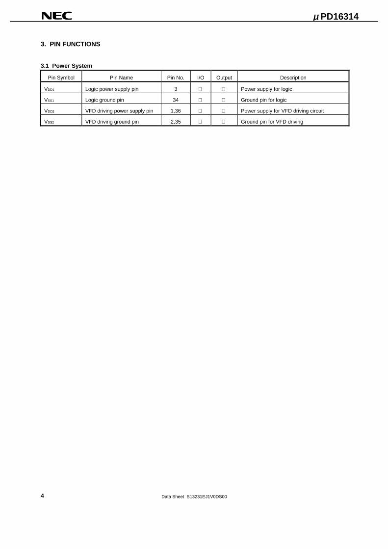
3. PIN FUNCTIONS
3.1 Power System
Pin Symbol Pin Name Pin No. I/O Output Description
VDD1 Logic power supply pin 3 Power supply for logic
VSS1 Logic ground pin 34 Ground pin for logic
VDD2 VFD driving power supply pin 1,36 Power supply for VFD driving circuit
VSS2 VFD driving ground pin 2,35 Ground pin for VFD driving
Data Sheet S13231EJ1V0DS00 5
µ µ µ µ PD16314
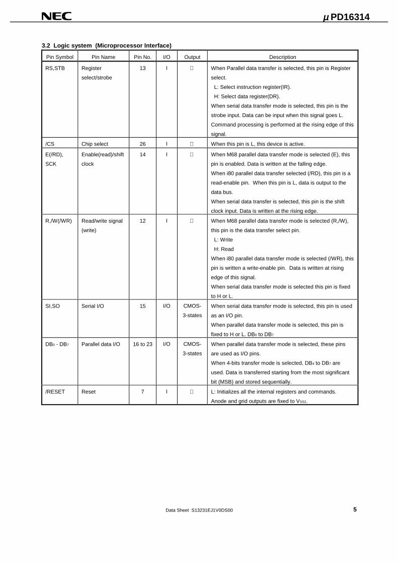
3.2 Logic system (Microprocessor Interface)
Pin Symbol Pin Name Pin No. I/O Output Description
RS,STB Register
select/strobe
13 I When Parallel data transfer is selected, this pin is Register
select.
L: Select instruction register(IR).
H: Select data register(DR).
When serial data transfer mode is selected, this pin is the
strobe input. Data can be input when this signal goes L.
Command processing is performed at the rising edge of this
signal.
/CS Chip select 26 I When this pin is L, this device is active.
E(/RD),
SCK
Enable(read)/shift
clock
14 I When M68 parallel data transfer mode is selected (E), this
pin is enabled. Data is written at the falling edge.
When i80 parallel data transfer selected (/RD), this pin is a
read-enable pin. When this pin is L, data is output to the
data bus.
When serial data transfer is selected, this pin is the shift
clock input. Data is written at the rising edge.
R,/W(/WR) Read/write signal
(write)
12 I When M68 parallel data transfer mode is selected (R,/W),
this pin is the data transfer select pin.
L: Write
H: Read
When i80 parallel data transfer mode is selected (/WR), this
pin is written a write-enable pin. Data is written at rising
edge of this signal.
When serial data transfer mode is selected this pin is fixed
to H or L.
SI,SO Serial I/O 15 I/O CMOS-
3-states
When serial data transfer mode is selected, this pin is used
as an I/O pin.
When parallel data transfer mode is selected, this pin is
fixed to H or L. DB0 to DB7
DB0 - DB7 Parallel data I/O 16 to 23 I/O CMOS-
3-states
When parallel data transfer mode is selected, these pins
are used as I/O pins.
When 4-bits transfer mode is selected, DB4 to DB7 are
used. Data is transferred starting from the most significant
bit (MSB) and stored sequentially.
/RESET Reset 7 I L: Initializes all the internal registers and commands.
Anode and grid outputs are fixed to VSS2.
Data Sheet S13231EJ1V0DS006
µ µ µ µ PD16314
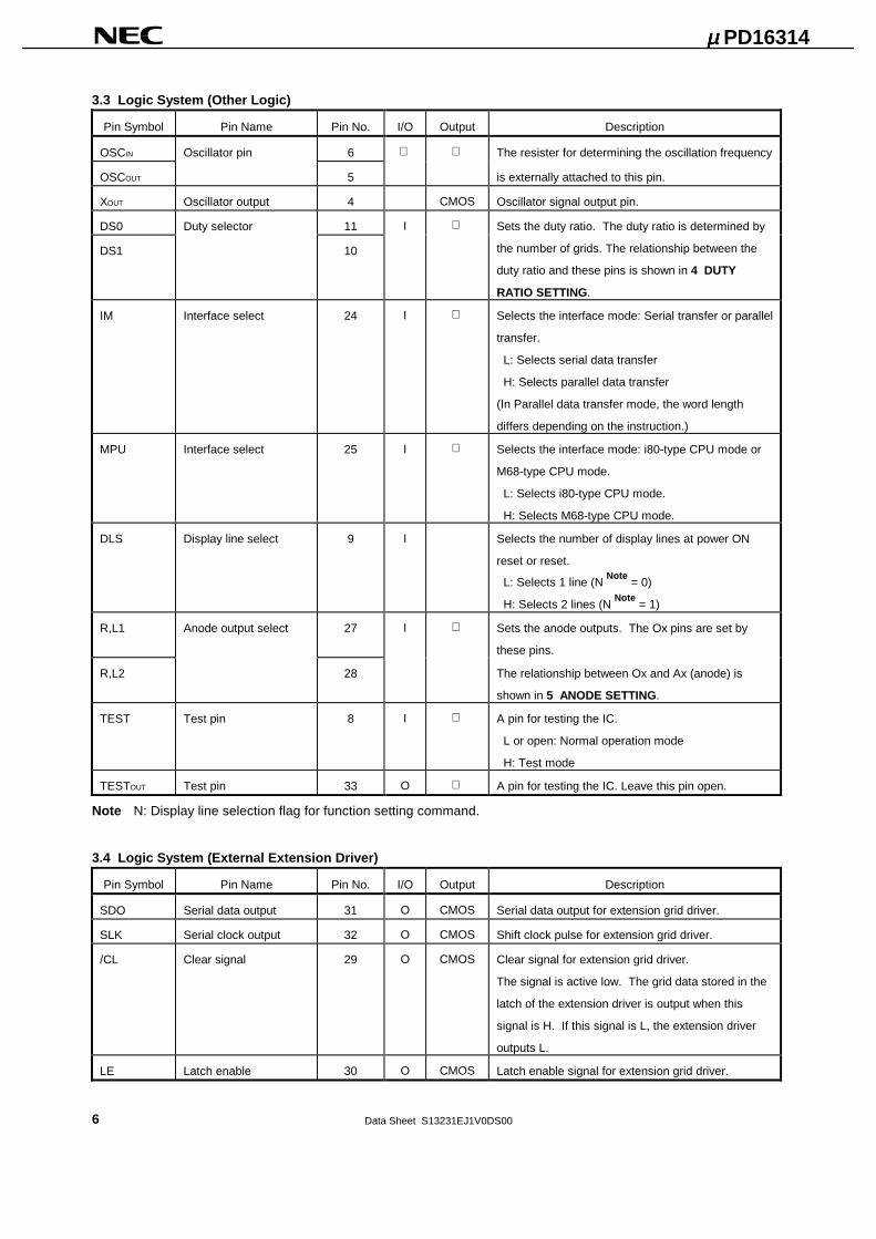
3.3 Logic System (Other Logic)
Pin Symbol Pin Name Pin No. I/O Output Description
OSCIN Oscillator pin 6 The resister for determining the oscillation frequency
OSCOUT 5 is externally attached to this pin.
XOUT Oscillator output 4 CMOS Oscillator signal output pin.
DS0 Duty selector 11 I
DS1 10
Sets the duty ratio. The duty ratio is determined by
the number of grids. The relationship between the
duty ratio and these pins is shown in 4 DUTY
RATIO SETTING.
IM Interface select 24 I Selects the interface mode: Serial transfer or parallel
transfer.
L: Selects serial data transfer
H: Selects parallel data transfer
(In Parallel data transfer mode, the word length
differs depending on the instruction.)
MPU Interface select 25 I Selects the interface mode: i80-type CPU mode or
M68-type CPU mode.
L: Selects i80-type CPU mode.
H: Selects M68-type CPU mode.
DLS Display line select 9 I Selects the number of display lines at power ON
reset or reset.
L: Selects 1 line (N Note
= 0)
H: Selects 2 lines (N Note
= 1)
R,L1 Anode output select 27 I Sets the anode outputs. The Ox pins are set by
these pins.
R,L2 28 The relationship between Ox and Ax (anode) is
shown in 5 ANODE SETTING.
TEST Test pin 8 I A pin for testing the IC.
L or open: Normal operation mode
H: Test mode
TESTOUT Test pin 33 O A pin for testing the IC. Leave this pin open.
Note N: Display line selection flag for function setting command.
3.4 Logic System (External Extension Driver)
Pin Symbol Pin Name Pin No. I/O Output Description
SDO Serial data output 31 O CMOS Serial data output for extension grid driver.
SLK Serial clock output 32 O CMOS Shift clock pulse for extension grid driver.
/CL Clear signal 29 O CMOS Clear signal for extension grid driver.
The signal is active low. The grid data stored in the
latch of the extension driver is output when this
signal is H. If this signal is L, the extension driver
outputs L.
LE Latch enable 30 O CMOS Latch enable signal for extension grid driver.

Data Sheet S13231EJ1V0DS00 7
µ µ µ µ PD16314
3.5 Output Pins
Pin Symbol Pin Name Pin No. I/O Output Description
G1 - G24 Grid output Note O CMOS Grid signal output pins.
A1 - A80
(O1 - O80)
Anode output Note O CMOS Anode signal output pins.
Note Refer to 4 DUTY RATIO SETTING.
Data Sheet S13231EJ1V0DS008
µ µ µ µ PD16314
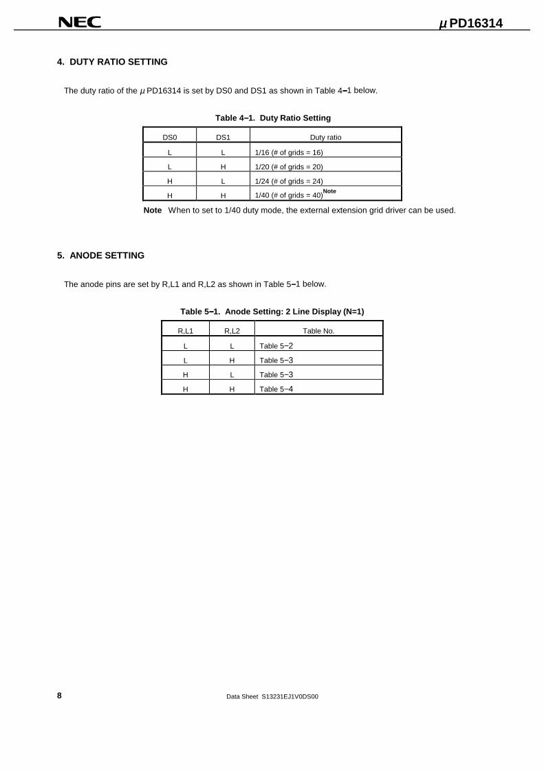
4. DUTY RATIO SETTING
The duty ratio of the µ PD16314 is set by DS0 and DS1 as shown in Table 4−−−−1 below.
Table 4 −−−−1. Duty Ratio Setting
DS0 DS1 Duty ratio
L L 1/16 (# of grids = 16)
L H 1/20 (# of grids = 20)
H L 1/24 (# of grids = 24)
H H 1/40 (# of grids = 40)Note
Note When to set to 1/40 duty mode, the external extension grid driver can be used.
5. ANODE SETTING
The anode pins are set by R,L1 and R,L2 as shown in Table 5−−−−1 below.
Table 5 −−−−1. Anode Setting: 2 Line Display (N=1)
R,L1 R,L2 Table No.
L L Table 5−2
L H Table 5−3
H L Table 5−3
H H Table 5−4

Data Sheet S13231EJ1V0DS00 9
µ µ µ µ PD16314
Table 5 −−−−2. Anode Pin Layout (When R,L1 = L, R,L2 = L)
No. Name No. Name No. Name No. Name
1 VDD2 37 N.C. 73 A35 109 N.C.
2 VSS2 38 A1 74 A36 110 A71
3 VDD1 39 A2 75 A37 111 A72
4 XOUT 40 A3 76 A38 112 A73
5 OSCOUT 41 A4 77 A39 113 A74
6 OSCIN 42 A5 78 A40 114 A75
7 /RESET 43 A6 79 A41 115 A76
8 TEST 44 A7 80 A42 116 A77
9 DLS 45 A8 81 A43 117 A78
10 DS1 46 A9 82 A44 118 A79
11 DS0 47 A10 83 A45 119 A80
12 R,/W(/WR) 48 A11 84 A46 120 G24
13 RS,STB 49 A12 85 A47 121 G23
14 E(/RD),SCK 50 A13 86 A48 122 G22
15 SI,SO 51 A14 87 A49 123 G21
16 DB0 52 A15 88 A50 124 G20
17 DB1 53 A16 89 A51 125 G19
18 DB2 54 A17 90 A52 126 G18
19 DB3 55 A18 91 A53 127 G17
20 DB4 56 A19 92 A54 128 G16
21 DB5 57 A20 93 A55 129 G15
22 DB6 58 A21 94 A56 130 G14
23 DB7 59 A22 95 A57 131 G13
24 IM 60 A23 96 A58 132 G12
25 MPU 61 A24 97 A59 133 G11
26 /CS 62 A25 98 A60 134 G10
27 R,L1 63 A26 99 A61 135 G9
28 R,L2 64 A27 100 A62 136 G8
29 /CL 65 A28 101 A63 137 G7
30 LE 66 A29 102 A64 138 G6
31 SDO 67 A30 103 A65 139 G5
32 SLK 68 A31 104 A66 140 G4
33 TESTOUT 69 A32 105 A67 141 G3
34 VSS1 70 A33 106 A68 142 G2
35 VSS2 71 A34 107 A69 143 G1
36 VDD2 72 N.C. 108 A70 144 N.C.

Data Sheet S13231EJ1V0DS0010
µ µ µ µ PD16314
Table 5 −−−−3. Anode Pin Layout (When R,L1 = L, R,L2 = H)
No. Name No. Name No. Name No. Name
1 VDD2 37 N.C. 73 A6 109 N.C.
2 VSS2 38 A40 74 A5 110 A71
3 VDD1 39 A39 75 A4 111 A72
4 XOUT 40 A38 76 A3 112 A73
5 OSCOUT 41 A37 77 A2 113 A74
6 OSCIN 42 A36 78 A1 114 A75
7 /RESET 43 A35 79 A41 115 A76
8 TEST 44 A34 80 A42 116 A77
9 DLS 45 A33 81 A43 117 A78
10 DS1 46 A32 82 A44 118 A79
11 DS0 47 A31 83 A45 119 A80
12 R,/W(/WR) 48 A30 84 A46 120 G24
13 RS,STB 49 A29 85 A47 121 G23
14 E(/RD),SCK 50 A28 86 A48 122 G22
15 SI,SO 51 A27 87 A49 123 G21
16 DB0 52 A26 88 A50 124 G20
17 DB1 53 A25 89 A51 125 G19
18 DB2 54 A24 90 A52 126 G18
19 DB3 55 A23 91 A53 127 G17
20 DB4 56 A22 92 A54 128 G16
21 DB5 57 A21 93 A55 129 G15
22 DB6 58 A20 94 A56 130 G14
23 DB7 59 A19 95 A57 131 G13
24 IM 60 A18 96 A58 132 G12
25 MPU 61 A17 97 A59 133 G11
26 /CS 62 A16 98 A60 134 G10
27 R,L1 63 A15 99 A61 135 G9
28 R,L2 64 A14 100 A62 136 G8
29 /CL 65 A13 101 A63 137 G7
30 LE 66 A12 102 A64 138 G6
31 SDO 67 A11 103 A65 139 G5
32 SLK 68 A10 104 A66 140 G4
33 TESTOUT 69 A9 105 A67 141 G3
34 VSS1 70 A8 106 A68 142 G2
35 VSS2 71 A7 107 A69 143 G1
36 VDD2 72 N.C. 108 A70 144 N.C.

Data Sheet S13231EJ1V0DS00 11
µ µ µ µ PD16314
Table 5 −−−−4. Anode Pin Layout (When R,L1 = H, R,L2 = L)
No. Name No. Name No. Name No. Name
1 VDD2 37 N.C. 73 A75 109 N.C.
2 VSS2 38 A41 74 A76 110 A10
3 VDD1 39 A42 75 A77 111 A9
4 XOUT 40 A43 76 A78 112 A8
5 OSCOUT 41 A44 77 A79 113 A7
6 OSCIN 42 A45 78 A80 114 A6
7 /RESET 43 A46 79 A40 115 A5
8 TEST 44 A47 80 A39 116 A4
9 DLS 45 A48 81 A38 117 A3
10 DS1 46 A49 82 A37 118 A2
11 DS0 47 A50 83 A36 119 A1
12 R,/W(/WR) 48 A51 84 A35 120 G24
13 RS,STB 49 A52 85 A34 121 G23
14 E(/RD),SCK 50 A53 86 A33 122 G22
15 SI,SO 51 A54 87 A32 123 G21
16 DB0 52 A55 88 A31 124 G20
17 DB1 53 A56 89 A30 125 G19
18 DB2 54 A57 90 A29 126 G18
19 DB3 55 A58 91 A28 127 G17
20 DB4 56 A59 92 A27 128 G16
21 DB5 57 A60 93 A26 129 G15
22 DB6 58 A61 94 A25 130 G14
23 DB7 59 A62 95 A24 131 G13
24 IM 60 A63 96 A23 132 G12
25 MPU 61 A64 97 A22 133 G11
26 /CS 62 A65 98 A21 134 G10
27 R,L1 63 A66 99 A20 135 G9
28 R,L2 64 A67 100 A19 136 G8
29 /CL 65 A68 101 A18 137 G7
30 LE 66 A69 102 A17 138 G6
31 SDO 67 A70 103 A16 139 G5
32 SLK 68 A71 104 A15 140 G4
33 TESTOUT 69 A72 105 A14 141 G3
34 VSS1 70 A73 106 A13 142 G2
35 VSS2 71 A74 107 A12 143 G1
36 VDD2 72 N.C. 108 A11 144 N.C.

Data Sheet S13231EJ1V0DS0012
µ µ µ µ PD16314
Table 5 −−−−5. Anode Pin Layout (When R,L1 = H, R,L2 = H)
No. Name No. Name No. Name No. Name
1 VDD2 37 N.C. 73 A46 109 N.C.
2 VSS2 38 A80 74 A45 110 A10
3 VDD1 39 A79 75 A44 111 A9
4 XOUT 40 A78 76 A43 112 A8
5 OSCOUT 41 A77 77 A42 113 A7
6 OSCIN 42 A76 78 A41 114 A6
7 /RESET 43 A75 79 A40 115 A5
8 TEST 44 A74 80 A39 116 A4
9 DLS 45 A73 81 A38 117 A3
10 DS1 46 A72 82 A37 118 A2
11 DS0 47 A71 83 A36 119 A1
12 R,/W 48 A70 84 A35 120 G24
13 RS,STB 49 A69 85 A34 121 G23
14 E(/RD),SCK 50 A68 86 A33 122 G22
15 SI,SO 51 A67 87 A32 123 G21
16 DB0 52 A66 88 A31 124 G20
17 DB1 53 A65 89 A30 125 G19
18 DB2 54 A64 90 A29 126 G18
19 DB3 55 A63 91 A28 127 G17
20 DB4 56 A62 92 A27 128 G16
21 DB5 57 A61 93 A26 129 G15
22 DB6 58 A60 94 A25 130 G14
23 DB7 59 A59 95 A24 131 G13
24 IM 60 A58 96 A23 132 G12
25 MPU 61 A57 97 A22 133 G11
26 /CS 62 A56 98 A21 134 G10
27 R,L1 63 A55 99 A20 135 G9
28 R,L2 64 A54 100 A19 136 G8
29 /CL 65 A53 101 A18 137 G7
30 LE 66 A52 102 A17 138 G6
31 SDO 67 A51 103 A16 139 G5
32 SLK 68 A50 104 A15 140 G4
33 TESTOUT 69 A49 105 A14 141 G3
34 VSS1 70 A48 106 A13 142 G2
35 VSS2 71 A47 107 A12 143 G1
36 VDD2 72 N.C. 108 A11 144 N.C.

Data Sheet S13231EJ1V0DS00 13
µ µ µ µ PD16314
Table 5 −−−−6. Anode Setting: 1 Line Display (N=0)
R,L1 R,L2 Table No.
Don’t care L Table 5−7
Don’t care H Table 5−8
Table 5 −−−−7. Anode Pin Layout (When R,L2 = L)
No. Name No. Name No. Name No. Name
1 VDD2 37 N.C. 73 A35 109 N.C.
2 VSS2 38 A1 74 A36 110 Unused
3 VDD1 39 A2 75 A37 111
4 XOUT 40 A3 76 A38 112
5 OSCOUT 41 A4 77 A39 113
6 OSCIN 42 A5 78 A40 114
7 /RESET 43 A6 79 Unused 115
8 TEST 44 A7 80 116
9 DLS 45 A8 81 117
10 DS1 46 A9 82 118
11 DS0 47 A10 83 119
12 R,/W 48 A11 84 120 G24
13 RS,STB 49 A12 85 121 G23
14 E(/RD),SCK 50 A13 86 122 G22
15 SI,SO 51 A14 87 123 G21
16 DB0 52 A15 88 124 G20
17 DB1 53 A16 89 125 G19
18 DB2 54 A17 90 126 G18
19 DB3 55 A18 91 127 G17
20 DB4 56 A19 92 128 G16
21 DB5 57 A20 93 129 G15
22 DB6 58 A21 94 130 G14
23 DB7 59 A22 95 131 G13
24 IM 60 A23 96 132 G12
25 MPU 61 A24 97 133 G11
26 /CS 62 A25 98 134 G10
27 R,L1 63 A26 99 135 G9
28 R,L2 64 A27 100 136 G8
29 /CL 65 A28 101 137 G7
30 LE 66 A29 102 138 G6
31 SDO 67 A30 103 139 G5
32 SLK 68 A31 104 140 G4
33 TESTOUT 69 A32 105 141 G3
34 VSS1 70 A33 106 142 G2
35 VSS2 71 A34 107 143 G1
36 VDD2 72 N.C. 108 144 N.C.

Data Sheet S13231EJ1V0DS0014
µ µ µ µ PD16314
Table 5 −−−−8. Anode Pin Layout (When R,L2 = H)
No. Name No. Name No. Name No. Name
1 VDD2 37 N.C. 73 A6 109 N.C.
2 VSS2 38 A40 74 A5 110 Unused
3 VDD1 39 A39 75 A4 111
4 XOUT 40 A38 76 A3 112
5 OSCOUT 41 A37 77 A2 113
6 OSCIN 42 A36 78 A1 114
7 /RESET 43 A35 79 Unused 115
8 TEST 44 A34 80 116
9 DLS 45 A33 81 117
10 DS1 46 A32 82 118
11 DS0 47 A31 83 119
12 R,/W 48 A30 84 120 G24
13 RS,STB 49 A29 85 121 G23
14 E(/RD),SCK 50 A28 86 122 G22
15 SI,SO 51 A27 87 123 G21
16 DB0 52 A26 88 124 G20
17 DB1 53 A25 89 125 G19
18 DB2 54 A24 90 126 G18
19 DB3 55 A23 91 127 G17
20 DB4 56 A22 92 128 G16
21 DB5 57 A21 93 129 G15
22 DB6 58 A20 94 130 G14
23 DB7 59 A19 95 131 G13
24 IM 60 A18 96 132 G12
25 MPU 61 A17 97 133 G11
26 /CS 62 A16 98 134 G10
27 R,L1 63 A15 99 135 G9
28 R,L2 64 A14 100 136 G8
29 /CL 65 A13 101 137 G7
30 LE 66 A12 102 138 G6
31 SDO 67 A11 103 139 G5
32 SLK 68 A10 104 140 G4
33 TESTOUT 69 A9 105 141 G3
34 VSS1 70 A8 106 142 G2
35 VSS2 71 A7 107 143 G1
36 VDD2 72 N.C. 108 144 N.C.

Data Sheet S13231EJ1V0DS00 15
µ µ µ µ PD16314
6. VFD DISPLAY
The µ PD16314 can display 24 characters x 2 lines, and a VFD can be connected as shown in the figure below.
Figure 6 −−−−1. VFD Display
A1
A5A6
A10
A71
A75A76
A80
A1
A40
A41
A80
G1G2
G24
PD
1631
4µ
Data Sheet S13231EJ1V0DS0016
µ µ µ µ PD16314
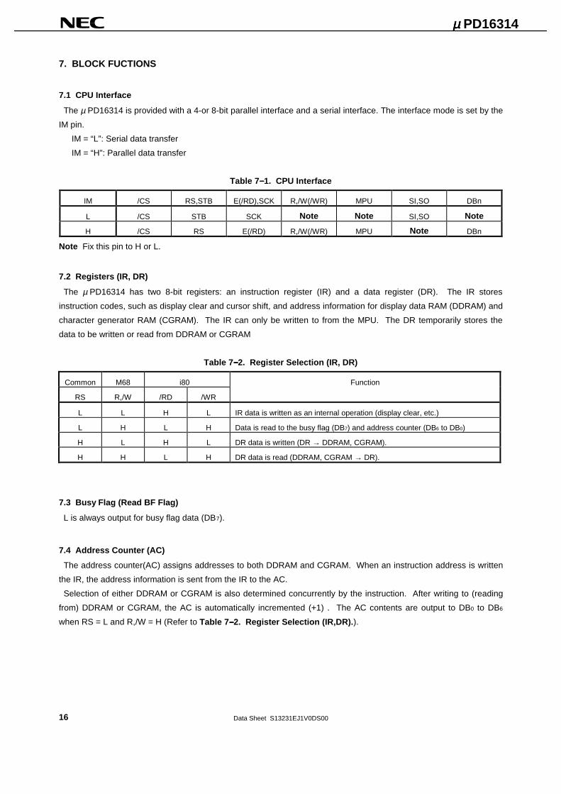
7. BLOCK FUCTIONS
7.1 CPU Interface
The µ PD16314 is provided with a 4-or 8-bit parallel interface and a serial interface. The interface mode is set by the
IM pin.
IM = “L”: Serial data transfer
IM = “H”: Parallel data transfer
Table 7 −−−−1. CPU Interface
IM /CS RS,STB E(/RD),SCK R,/W(/WR) MPU SI,SO DBn
L /CS STB SCK Note Note SI,SO Note
H /CS RS E(/RD) R,/W(/WR) MPU Note DBn
Note Fix this pin to H or L.
7.2 Registers (IR, DR)
The µ PD16314 has two 8-bit registers: an instruction register (IR) and a data register (DR). The IR stores
instruction codes, such as display clear and cursor shift, and address information for display data RAM (DDRAM) and
character generator RAM (CGRAM). The IR can only be written to from the MPU. The DR temporarily stores the
data to be written or read from DDRAM or CGRAM
Table 7 −−−−2. Register Selection (IR, DR)
Common M68 i80 Function
RS R,/W /RD /WR
L L H L IR data is written as an internal operation (display clear, etc.)
L H L H Data is read to the busy flag (DB7) and address counter (DB6 to DB0)
H L H L DR data is written (DR → DDRAM, CGRAM).
H H L H DR data is read (DDRAM, CGRAM → DR).
7.3 Busy Flag (Read BF Flag)
L is always output for busy flag data (DB7).
7.4 Address Counter (AC)
The address counter(AC) assigns addresses to both DDRAM and CGRAM. When an instruction address is written
the IR, the address information is sent from the IR to the AC.
Selection of either DDRAM or CGRAM is also determined concurrently by the instruction. After writing to (reading
from) DDRAM or CGRAM, the AC is automatically incremented (+1) . The AC contents are output to DB0 to DB6
when RS = L and R,/W = H (Refer to Table 7 −−−−2. Register Selection (IR,DR). ).
Data Sheet S13231EJ1V0DS00 17
µ µ µ µ PD16314
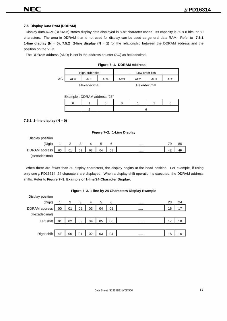
7.5 Display Data RAM (DDRAM)
Display data RAM (DDRAM) stores display data displayed in 8-bit character codes. Its capacity is 80 x 8 bits, or 80
characters. The area in DDRAM that is not used for display can be used as general data RAM. Refer to 7.5.1
1-line display (N = 0), 7.5.2 2-line display (N = 1) for the relationship between the DDRAM address and the
position on the VFD.
The DDRAM address (ADD) is set in the address counter (AC) as hexadecimal.
Figure 7 −1. DDRAM Address
High-order bits Low-order bits
AC AC6 AC5 AC4 AC3 AC2 AC1 AC0
Hexadecimal Hexadecimal
Example : DDRAM address “26”
0 1 0 0 1 1 0
2 6
7.5.1 1-line display (N = 0)
Figure 7 −−−−2. 1-Line Display
Display position
(Digit) 1 2 3 4 5 6 ....... 79 80
00 01 02 03 04 05 ....... 4E 4FDDRAM address
(Hexadecimal)
When there are fewer than 80 display characters, the display begins at the head position. For example, if using
only one µ PD16314, 24 characters are displayed. When a display shift operation is executed, the DDRAM address
shifts. Refer to Figure 7−3. Example of 1-line/24-Character Display.
Figure 7 −−−−3. 1-line by 24 Characters Display Example
Display position
(Digit) 1 2 3 4 5 6 ..... 23 24
00 01 02 03 04 05 ..... 16 17DDRAM address
(Hexadecimal)
Left shift 01 02 03 04 05 06 ..... 17 18
Right shift 4F 00 01 02 03 04 ..... 15 16
Data Sheet S13231EJ1V0DS0018
µ µ µ µ PD16314
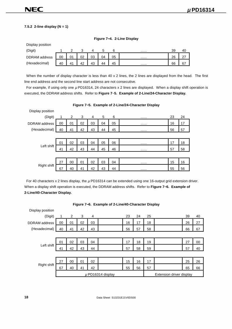
7.5.2 2-line display (N = 1)
Figure 7 −−−−4. 2-Line Display
Display position
(Digit) 1 2 3 4 5 6 ....... 39 40
00 01 02 03 04 05 ....... 26 27DDRAM address
(Hexadecimal) 40 41 42 43 44 45 ....... 66 67
When the number of display character is less than 40 x 2 lines, the 2 lines are displayed from the head. The first
line end address and the second line start address are not consecutive.
For example, if using only one µ PD16314, 24 characters x 2 lines are displayed. When a display shift operation is
executed, the DDRAM address shifts. Refer to Figure 7 −5. Example of 2-Line/24-Character Display.
Figure 7 −−−−5. Example of 2-Line/24-Character Display
Display position
(Digit) 1 2 3 4 5 6 ....... 23 24
00 01 02 03 04 05 ....... 16 17DDRAM address
(Hexadecimal) 40 41 42 43 44 45 ....... 56 57
01 02 03 04 05 06 ....... 17 18Left shift
41 42 43 44 45 46 ....... 57 58
27 00 01 02 03 04 ....... 15 16Right shift
67 40 41 42 43 44 ....... 55 56
For 40 characters x 2 lines display, the µ PD16314 can be extended using one 16-output grid extension driver.
When a display shift operation is executed, the DDRAM address shifts. Refer to Figure 7 −−−−6. Example of
2-Line/40-Character Display.
Figure 7 −−−−6. Example of 2-Line/40-Character Display
Display position
(Digit) 1 2 3 4 23 24 25 39 40
00 01 02 03 16 17 18 26 27DDRAM address
(Hexadecimal) 40 41 42 43 56 57 58 66 67
01 02 03 04 17 18 19 27 00Left shift
41 42 43 44 57 58 59 57 40
27 00 01 02 15 16 17 25 26Right shift
67 40 41 42 55 56 57 65 66
µ PD16314 display Extension driver display

Data Sheet S13231EJ1V0DS00 19
µ µ µ µ PD16314
7.6 Character Generator ROM (CGROM)
CGROM, which is ROM for generating character patterns of 5 x 8 dots from 8-bit character codes, generates 240
types of character patterns.
The character codes are shown on the following page. The character codes 00H to 0FH are allocated to the
CGRAM.

Data Sheet S13231EJ1V0DS0020
µ µ µ µ PD16314
Figure 7 −−−−7. Character Code Table 1 (ROM code: 001)
XXXX0000 0CG
RAM(0)
0 1 2 3 4 5 6 7 8 9 A B C D E F
XXXX0001 1CG
RAM(1)
XXXX0010 2CG
RAM(2)
XXXX0011 3CG
RAM(3)
XXXX0100 4CG
RAM(4)
XXXX0101 5CG
RAM(5)
XXXX0110 6CG
RAM(6)
XXXX0111 7CG
RAM(7)
XXXX1000 8CG
RAM(0)
XXXX1001 9CG
RAM(1)
XXXX1010 ACG
RAM(2)
XXXX1011 BCG
RAM(3)
XXXX1100 CCG
RAM(4)
XXXX1101 DCG
RAM(5)
XXXX1110 ECG
RAM(6)
XXXX1111 FCG
RAM(7)

Data Sheet S13231EJ1V0DS00 21
µ µ µ µ PD16314
Figure 7 −−−−8. Character Code Table 2 (ROM code: 002)
XXXX0000 0CG
RAM(0)
0 1 2 3 4 5 6 7 8 9 A B C D E F
XXXX0001 1CG
RAM(1)
XXXX0010 2CG
RAM(2)
XXXX0011 3CG
RAM(3)
XXXX0100 4CG
RAM(4)
XXXX0101 5CG
RAM(5)
XXXX0110 6CG
RAM(6)
XXXX0111 7CG
RAM(7)
XXXX1000 8CG
RAM(0)
XXXX1001 9CG
RAM(1)
XXXX1010 ACG
RAM(2)
XXXX1011 BCG
RAM(3)
XXXX1100 CCG
RAM(4)
XXXX1101 DCG
RAM(5)
XXXX1110 ECG
RAM(6)
XXXX1111 FCG
RAM(7)

Data Sheet S13231EJ1V0DS0022
µ µ µ µ PD16314
7.7 Character Generator RAM (CGRAM)
With character generator RAM (CGRAM), the user can rewrite character patterns by program. For 5 x 8 dots, 8-
character patterns can be written.
Character codes 00H to 07H and 08H to 0FH have the same CGRAM contents.
Refer to Figure 7 −−−−9 for the relationship between the CGRAM address and data and display patterns . Areas
that are not used for display can be used as general data RAM.
Figure 7 −−−−9. Relationship between the CGRAM Address, Character Code (DDRAM)
and 5 x 7 (With Cursor) Dot Character Patterns (CGRAM)
Character code (DDRAM data) CGRAM address CGRAM data
D7
0
0
0
High-order bits High-order bits High-order bitsLow-order bits Low-order bits Low-order bits
D6
0
0
0
D5
0
0
0
D4
0
0
0
D3
x
x
x
D2
0
0
1
D1
0
0
1
D0
0
1
1
A5
0
0
1
A4
0
0
1
A3
0
1
1
A2
0
0
0
0
1
1
1
1
0
0
0
0
1
1
1
1
0
0
0
0
1
1
1
1
A1
0
0
1
1
0
0
1
1
0
0
1
1
0
0
1
1
0
0
1
1
0
0
1
1
A0
0
1
0
1
0
1
0
1
0
1
0
1
0
1
0
1
0
1
0
1
0
1
0
1
D7
x
x
x
D6
x
x
x
D5
x
x
x
D4
1
1
1
1
1
1
1
0
1
1
1
1
1
1
1
0
0
1
1
1
1
1
0
1
D3
0
0
1
0
0
0
0
0
1
0
0
1
0
0
1
0
1
0
0
0
0
0
1
1
D2
0
0
0
1
0
0
0
0
1
0
0
1
0
0
1
0
1
0
0
0
0
0
1
1
D1
0
0
0
0
1
0
0
0
1
0
0
1
0
0
1
0
1
0
0
0
0
0
1
1
D0
1
1
1
1
1
1
1
0
1
0
0
1
0
0
1
0
0
1
0
0
0
1
0
1
Character
pattern (0)
Cursor position
Character
pattern (1)
Cursor position
Cursor position
Character
pattern (7)
Remarks 1. x: Don’t care.
2.Character code bits 0 to 2 correspond to CGRAM address bits 3 to 5 (3 bits: 8 types).
3.CGRAM address bits 0 to 2 designate the character pattern line position. The 8th line is the
cursor position and its display is formed by a logical OR with the cursor specification. If the 8th
line data is made 0, the display is determined by the cursor specifiaction. If the 8th line data is 1,
the 8th line will light up regardless of the cursor presence.
4.1 for CGRAM data corresponds to display selection and 0 to non selection.

Data Sheet S13231EJ1V0DS00 23
µ µ µ µ PD16314
7.8 Timing Generator
The timing generator generates timing signals for the operation of internal circuits such as DDRAM, CGRAM and
CGROM. The RAM read timing for display and internal operation timing by MPU access are generated separately to
avoid interference. Therefore, when writing data to DDRAM, for example, there will be no undesirable interference,
such as flickering, in areas other than the display area.
7.9 VFD Driver Circuit
The VFD driver circuit consists of 24 grid signal drivers and 80 anode signal drivers. When the character font and
number of digits are selected, the required grid signal drivers automatically output drive waveforms.
7.10 Cursor/Blink Control Circuit
The cursor/blink control circuit generates the cursor or character blink. The cursor or blink is valid at the digit
located at the display data RAM (DDRAM) address set in the address counter (AC).
For example, when the address counter is 08H, the cursor position is displayed at DDRAM address 08H.
Figure 7 −−−−10. Cursor/Blink Control
AC6 AC5 AC4 AC3 AC2 AC1 AC0
AC 0 0 0 1 0 0 0
For 1-line display
Display position
(Digit) 1 2 3 4 5 6 7 8 9 10 11 12
00 01 02 03 04 05 06 07 08 09 0A 0BDDRAM address
(Hexadecimal)
Cursor position
For 2-line display
Display position
(Digit) 1 2 3 4 5 6 7 8 9 10 11 12
00 01 02 03 04 05 06 07 08 09 0A 0BDDRAM address
(Hexadecimal) 40 41 42 43 44 45 46 47 48 49 4A 4B
Cursor position

Data Sheet S13231EJ1V0DS0024
µ µ µ µ PD16314
8. INTERFACING WITH CPU (DATA TRANSFER)
8.1 Parallel Data Transfer M68 (IM = H, MPU = H)
This IC can interface (data transfer) with the CPU in 4 or 8 bits (M68 interface: IM = H, MPU = H).
However, because the internal registers consist of 8 bits, when transfering data in 4 bits DB4 to DB7 must be used
twice. When using 4-bit parallel data transfer, maintain the DB0 to DB3 pins at H or L. The transfer order is the higher
4 bits first (D4 to D7) followed by the lower 4 bits (D0 to D3).
Figure 8 −−−−1. Parallel Data Transfer M68 (IM = H, MPU = H)
IR7 IR3 IR7DB7
R,/W
E
RS
IR3 D7 D3IR3BF = "0"
IR6 IR2 IR6DB6 IR2 D6 D2IR2
IR5 IR1 IR5DB5 IR1 D5 D1IR1
IR4 IR0 IR4DB4 IR0 D4 D0IR0
IR6
IR5
IR4
Writeinstruction
Writeinstruction
Readinstruction
Writedata
(a) 4-bit data transfer (M68)
IR7 IR7DB7
R,/W
E
RS
D7
IR6 IR6DB6 D6
IR0 IR0DB0 D0
IR6
IR0
Writeinstruction
Writeinstruction
Readinstruction
Writedata
BF = "0"
(b) 8-bit data transfer (M68)

Data Sheet S13231EJ1V0DS00 25
µ µ µ µ PD16314
8.2 Parallel Data Transfer i80 (IM = H, MPU = L)
When IM = H, MPU = L is set, i80 is selected. In the µ PD16314, each time data is sent to and from the CPU, the
data is retained the bus holder attached to internal data bus, and is written to the display data RAM by the next data
write cycle. When the CPU reads the contents of the display data RAM, the read data is retained in the bus holder
for the first data read cycle (dummy), and is read out on the system bus at the next data read cycle.
There are certain restrictions in the read sequence of this display data RAM. Be advised that data of the specified
address is not generated by the read instruction issued immediately after the address setting. This data is generated
when the data is read of the second time. Thus, a dummy read is required following an address setting or write cycle.
This relationship is shown in following figure.
Figure 8 −−−−2. Parallel Data Transfer i80 (IM = H, MPU = L)
N N n n+1
Preset N Increment N+1 N+2
/RD
Data
Read
signal
/WR
N n n+1 n+2BUS
holder
Address
preset
Column
address
Address set#n
Dummyread
Data read#n
Data read#n+1
Internal timing
MPU
N N+1 N+2 N+3
N N+1 N+2 N+3
/WR
Data
BUS
holder
Write
signal
Latch
MPU
Internal timing
Writing
Reading

Data Sheet S13231EJ1V0DS0026
µ µ µ µ PD16314
8.3 Serial Data Transfer
This IC can interface (data transfer) with the CPU in serial.
Data can be written when STB = L. The first byte is the start byte. The IR or the DR is selected by the RS bit(bit 6)
and data write or read by R,/W(bit 5 = 0). The next first bytes are instructions on data.
When data is read, whether to read the busy flag + address counter (AC6 to AC0) or to read the data written in
DDRAM or CGRAM is chosen by the start byte input first. Data is output at the falling edge of the shift clock.
Figure 8 −−−−3. Serial Data Transfer
1 2 3
Synchronous bits
4 5 6 7 8 9 10 11 12 13 14 15 16
SI
SCK
STB
Start byte Instruction/Data
R,W RS D7 D6 D5 D4 D3 D2 D1 D0
STB
Data write
Data read
1 2 3 4 5 6 7 8 1 2 3 4 5 6 7 8
R,W RS IR6 IR5 IR4 IR3 IR2 IR1 IR0
Synchronous bits
Start byte Read data
SI,SO
SCK
Wait time : tWAIT
1 s
9
17
µ
"0"
"0""1" "1" "1" "1" "1"
"1" "1" "1" "1" "1" "0"BF
Data Sheet S13231EJ1V0DS00 27
µ µ µ µ PD16314
9. INSTRUCTIONS
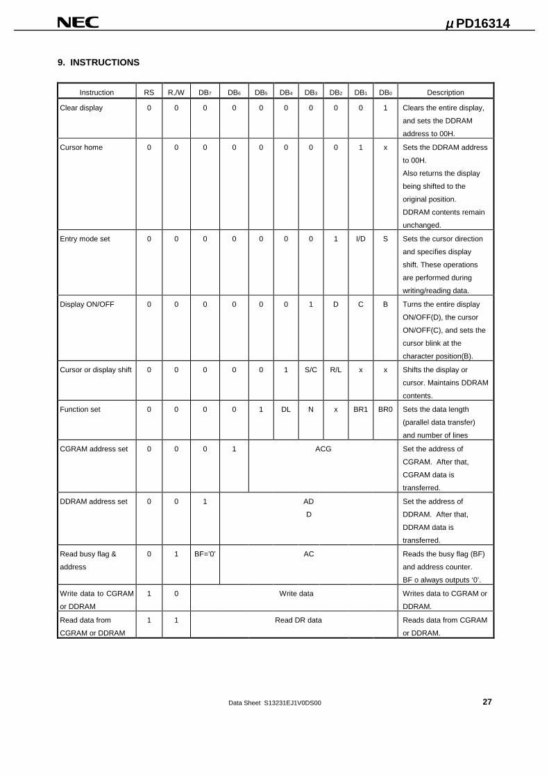
Instruction RS R,/W DB7 DB6 DB5 DB4 DB3 DB2 DB1 DB0 Description
Clear display 0 0 0 0 0 0 0 0 0 1 Clears the entire display,
and sets the DDRAM
address to 00H.
Cursor home 0 0 0 0 0 0 0 0 1 x Sets the DDRAM address
to 00H.
Also returns the display
being shifted to the
original position.
DDRAM contents remain
unchanged.
Entry mode set 0 0 0 0 0 0 0 1 I/D S Sets the cursor direction
and specifies display
shift. These operations
are performed during
writing/reading data.
Display ON/OFF 0 0 0 0 0 0 1 D C B Turns the entire display
ON/OFF(D), the cursor
ON/OFF(C), and sets the
cursor blink at the
character position(B).
Cursor or display shift 0 0 0 0 0 1 S/C R/L x x Shifts the display or
cursor. Maintains DDRAM
contents.
Function set 0 0 0 0 1 DL N x BR1 BR0 Sets the data length
(parallel data transfer)
and number of lines
CGRAM address set 0 0 0 1 ACG Set the address of
CGRAM. After that,
CGRAM data is
transferred.
DDRAM address set 0 0 1 AD
D
Set the address of
DDRAM. After that,
DDRAM data is
transferred.
Read busy flag &
address
0 1 BF=’0’ AC Reads the busy flag (BF)
and address counter.
BF o always outputs ‘0’.
Write data to CGRAM
or DDRAM
1 0 Write data Writes data to CGRAM or
DDRAM.
Read data from
CGRAM or DDRAM
1 1 Read DR data Reads data from CGRAM
or DDRAM.
Data Sheet S13231EJ1V0DS0028
µ µ µ µ PD16314
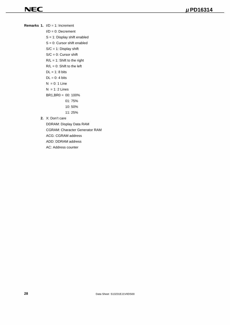
Remarks 1. I/D = 1: Increment
I/D = 0: Decrement
S = 1: Display shift enabled
S = 0: Cursor shift enabled
S/C = 1: Display shift
S/C = 0: Cursor shift
R/L = 1: Shift to the right
R/L = 0: Shift to the left
DL = 1: 8 bits
DL = 0: 4 bits
N = 0: 1 Line
N = 1: 2 Lines
BR1,BR0 = 00: 100%
01: 75%
10: 50%
11: 25%
2. X: Don’t care
DDRAM: Display Data RAM
CGRAM: Character Generator RAM
ACG: CGRAM address
ADD: DDRAM address
AC: Address counter

Data Sheet S13231EJ1V0DS00 29
µ µ µ µ PD16314
10. INSTRUCTION DESCRIPTION
10.1 Clear Display
RS R,/W DB7 DB6 DB5 DB4 DB3 DB2 DB1 DB0
Code 0 0 0 0 0 0 0 0 0 1
This instruction:
(1) Writes to 20H (Space code) all locations in display data RAM (DDRAM)
(2) Sets the address counter (AC) to the DDRAM address 00H.
(3) Returns the display Shift to 0.
(4) If cursor is displayed, the cursor is moved to the far left edge of the top line (upper line).
After reset:
DB7 DB6 DB5 DB4 DB3 DB2 DB1 DB0
0 0 0 0 0 0 0 1
10.2 Cursor Home
RS R,/W DB7 DB6 DB5 DB4 DB3 DB2 DB1 DB0
Code 0 0 0 0 0 0 0 0 0 x
This instruction:
(1) Sets the address counter (AC) to the DDRAM address 00H.
(2) Returns the display Shift to 0.
(3) If cursor is displayed, the cursor is held at the far edge of left the top line (upper line).

Data Sheet S13231EJ1V0DS0030
µ µ µ µ PD16314
10.3 Entry Mode
RS R,/W DB7 DB6 DB5 DB4 DB3 DB2 DB1 DB0
Code 0 0 0 0 0 0 0 1 I/D S
The I/D determines the way in which the contents of address counter are modified after every access to DDRAM or
CGRAM.
I/D = 1: Address counter incremented after access to DDRAM or CGRAM.
I/D = 0: Address counter decremented after access to DDRAM or CGRAM.
The S bit determines a display shift whether or a cursor shift occurs after each write or read to/from DDRAM.
S = 1: Display shift enabled.
S = 0: Cursor shift enabled.
The direction in which the display is shifted is the opposite to that of the cursor.
For example, if S = 0 and I/D = 1, cursor would shift one character to the right after a CPU write to DDRAM. However
if S = 1 and I/D = 1, the display would shift one character to the left and cursor would maintain its position on the
panel.
Note that the cursor is shifted in the direction selected by I/D when DDRAM is read, irrespective of the value of S.
Similarly reading and writing CGRAM always causes the cursor to shift.
Table 10 −−−−1. Cursor Move and Display Shift by Entry Mode Setting
I/D S After Writing DDRAM Data After Reading DDRAM Data
0 0 Cursor moves one character to the left. Cursor moves one character to the left.
1 0 Cursor moves one character to the right. Cursor moves one character to the right.
0 1 Display shifts one character to the right without
cursor moving.
Cursor moves one character to the left.
1 1 Display shifts one character to the left without
cursor moving.
Cursor moves one character to the right.
After reset:
DB7 DB6 DB5 DB4 DB3 DB2 DB1 DB0
0 0 0 0 0 1 1 0

Data Sheet S13231EJ1V0DS00 31
µ µ µ µ PD16314
10.4 Display ON/OFF
RS R,/W DB7 DB6 DB5 DB4 DB3 DB2 DB1 DB0
Code 0 0 0 0 0 0 1 D C B
This instruction controls various features of the display.
D = 1: Display on, D = 0: Display off.
C = 1: Cursor on, C = 0: Cursor off.
B = 1: Blink on, B = 0: Blink off.
Blinking is achieved by alternating between a normal and all-on display of a character.
The cursor blinks with a frequency of 1 Hz and a duty of 50 %.
Blink(1 Hz)
Cursor line
After reset:
DB7 DB6 DB5 DB4 DB3 DB2 DB1 DB0
0 0 0 0 1 0 0 0
10.5 Cursor or Display Shift
RS R,/W DB7 DB6 DB5 DB4 DB3 DB2 DB1 DB0
Code 0 0 0 0 0 1 S/C R/L x x
This instruction shifts the display and/or moves the cursor, one character to the left or right, without reading or
writing to DDRAM.
The S/C bit selects movement of the cursor or movement of both the cursor and display.
S/C = 1: Shifts both the cursor and display.
S/C = 0: Shifts only the cursor.
The R/L bit selects whether to move the display and/or cursor to the left or right.
R/L = 1 : Shift one character to the right.
R/L = 0 : Shift one character to the left.
Table 10 −−−−2. Cursor or Display Shift
S/C R/L Cursor Display
0 0 Moves one character to the left. No shift.
0 1 Moves one character to the right. No shift.
1 0 Moves one character to the left with the display. Shifts one character to the left.
1 1 Moves one character to the right with the display. Shifts one character to the right.

Data Sheet S13231EJ1V0DS0032
µ µ µ µ PD16314
10.6 Function Setting
RS R,/W DB7 DB6 DB5 DB4 DB3 DB2 DB1 DB0
Code 0 0 0 0 1 DL N x BR1 BR0
This instruction sets the data length of the data bus line (when using the parallel interface, IM = H), the number of
display lines and the brightness adjustment.
This instruction initializes the system, and must be the first instruction executed after power-on.
DL = 1: 8-bit CPU interface using DB7 to DB0
DL = 0: 4-bit CPU interface using DB7 to DB4
N = 0: Selects 1-line display (using anode outputs A1 to A40. A41 to A80 are fixed to low .).
N = 1: Selects 2-line display (using anode outputs A1 to A80).
The BR1, BR0 flags control the brightness of VFD by adjusting the to pulse width of the anode outputs as follows.
tDSP ≅ 200 µ s, tBLK ≅ 10 µ s
BR1 BR0 Brightness tp
0 0 100 % tDSP x 1.00
0 1 75 % tDSP x 0.75
1 0 50 % tDSP x 0.50
1 1 25 % tDSP x 0.25
tDSP
tp
tBLKAn
G1
Gn
T
tBLK
Remark n: Number of grids, T = n x (tDSP + tBLK)
After reset:
DB7 DB6 DB5 DB4 DB3 DB2 DB1 DB0
0 0 1 1 1 0 0 0
Data Sheet S13231EJ1V0DS00 33
µ µ µ µ PD16314
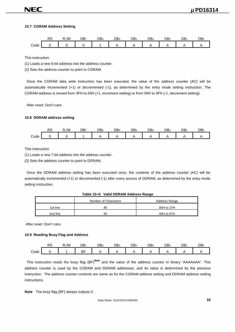
10.7 CGRAM Address Setting
RS R,/W DB7 DB6 DB5 DB4 DB3 DB2 DB1 DB0
Code 0 0 0 1 A A A A A A
This instruction:
(1) Loads a new 6-bit address into the address counter.
(2) Sets the address counter to point to CGRAM.
Once the CGRAM data write instruction has been executed, the value of the address counter (AC) will be
automatically incremented (+1) or decremented (-1), as determined by the entry mode setting instruction. The
CGRAM address is moved from 3FH to 00H (+1, increment setting) or from 00H to 3FH (-1, decrement setting).
After reset: Don’t care.
10.8 DDRAM address setting
RS R,/W DB7 DB6 DB5 DB4 DB3 DB2 DB1 DB0
Code 0 0 1 A A A A A A A
This instruction:
(1) Loads a new 7-bit address into the address counter.
(2) Sets the address counter to point to DDRAM.
Once the DDRAM address setting has been executed once, the contents of the address counter (AC) will be
automatically incremented (+1) or decremented (-1) after every access of DDRAM, as determined by the entry mode
setting instruction.
Table 10 −−−−3. Valid DDRAM Address Range
Number of Characters Address Range
1st line 40 00H to 27H
2nd line 40 40H to 67H
After reset: Don’t care.
10.9 Reading Busy Flag and Address
RS R,/W DB7 DB6 DB5 DB4 DB3 DB2 DB1 DB0
Code 0 1 BF A A A A A A A
This instruction reads the busy flag (BF)Note and the value of the address counter in binary “AAAAAAA”. This
address counter is used by the CGRAM and DDRAM addresses, and its value is determined by the previous
instruction. The address counter contents are same as for the CGRAM address setting and DDRAM address setting
instructions.
Note The busy flag (BF) always outputs 0.

Data Sheet S13231EJ1V0DS0034
µ µ µ µ PD16314
10.10 Writing Data to CGRAM or DDRAM
RS R,/W DB7 DB6 DB5 DB4 DB3 DB2 DB1 DB0
Code 1 0 D D D D D D D D
←High-order bits Low-order bits→
This instruction writes 8-bit binary data “DDDDDDDD” to CGRAM or DDRAM.
Whether to write to CGRAM or DDRAM is determined by the following instruction of CGRAM address setting or
DDRAM address setting. After a data write, the value address is automatically incremented or decremented by 1
according to the entry mode set. The entry mode also determines the display shift.
10.11 Reading Data from CGRAM or DDRAM
RS R,/W DB7 DB6 DB5 DB4 DB3 DB2 DB1 DB0
Code 1 1 D D D D D D D D
←High-order bits Low-order bits→
This instruction reads 8-bit binary data “DDDDDDDD” from CGRAM or DDRAM.
The previous specification determines whether CGRAM or DDRAM is to be read. Before entering this instruction,
either the CGRAM address setting or the DDRAM address setting instruction must be executed. If neither is
executed, the first read data is invalid, so when consecutively executing read instructions, the next address data is
normally read from the second read. The address setting instructions do not need to be executed just before this
read instruction, when the cursor is shifted by the cursor or display shift instruction (only when reading out data from
DDRAM).
The operation of the cursor shift instruction is the same as the DDRAM address setting instruction. After reading
one data, the value of the address is automatically incremented or decremented by 1 according to the entry mode
selection.
Caution The address counter is automatically incremented or decremented by 1 after the data write
instruction to CGRAM or DDRAM is executed. However, even if the contents of the RAM to be data
read instruction is executed indicated by the address counter cannot be read.
Therefore, to read the data correctly, execute the address setting instruction or the cursor shift
instruction (only in the case of DDRAM data read) just before reading, or, read from the second data
in the case of executing the consecutive read data instruction.

Data Sheet S13231EJ1V0DS00 35
µ µ µ µ PD16314
10.12 Power On Reset
The Internal status of µ PD16314 is initialized as follows after the power supply is turned on.
(1) Display clear: DDRAM is filled with 20H (space code).
(2) The address counter is set to 00H.
The address counter is set to point to DDRAM.
(3) Display ON/OFF: D = 0, C = 0, B = 0
(4) Entry mode set: I/D = 1, S = 0
(5) Function set: DL = 1, N = 1
(6) Brightness adjustment: BR0 = BR1 = 0
(7) The CPU interface and duty ratio selection are based on Table 10−4.
Table 10 −−−−4. Relationship between Status of µ µ µ µ PD16314 and Pin Selection at Power on Reset
Pin Name Function Remark
TEST IM DS1 DS0
H x x x Self test mode
L or open L x x Serial interface SI,SO, SCK, STB used
L or open H x x Parallel interface RS, E, R,/W, DB7 to DB4, or DB7 to DB0 used
L or open x L L Duty = 1/16 (16C x 1 or 2L display) The extension driver does not need to be used.
L or open x L H Duty = 1/20 (20C x 1 or 2L display) The number of lines is selected
L or open x H L Duty = 1/24 (24C x 1 or 2L display) by insutruction.
L or open x H H Duty = 1/40 (40C x 1 or 2L display) The extension driver should be used.
The number of lines is selected by instruction.
Remark X: Don’t care

Data Sheet S13231EJ1V0DS0036
µ µ µ µ PD16314
11. EXAMPLE OF DATA TRANSFER (8-bit Parallel, Data Increment Mode)
Figure 11 −−−−1. Initialization and Data Setting Procedure
Power ON
Function setting
CGRAM address setting
Data write
End of data write
DDRAM address setting
Data write
End of Data write
Display ON/OFF
No
No
All registers set to initialized value.
Set data length, display line number and display brightness.
Write the data to CGRAM.
Write the data to DDRAM.
Display ON
Yes
Yes
Table 11 −−−−1. Example of Initialization and Data Setting (M68 Series CPU)
RS R,/W D7 D6 D5 D4 D3 D2 D1 D0
Power ON
0 0 0 0 1 1 1 x 0 1 Function setting
Data length: 8 bits,
Display line number: 2 lines
VFD brightness: 75%
0 0 0 1 0 0 0 0 0 0 CGRAM address set to 00H
x x x D D D D D
x x x D D D D D
1 0
x x x D D D D D
Write data to CGRAM
64 bytes (8 characters)
0 0 1 0 0 0 0 0 0 0 DDRAM address set to 00H
D D D D D D D D
D D D D D D D D
1 0
D D D D D D D D
Write data to DDRAM
80 bytes (80 characters)
0 0 0 0 0 0 1 1 0 0 Display ON, cursor OFF, cursor blink OFF

Data Sheet S13231EJ1V0DS00 37
µ µ µ µ PD16314
12. ELECTRICAL SPECIFICATIONS
Absolute Maximum Ratings (T A = 25 °°°°C, VSS1 = VSS2 = 0 V)
Parameter Symbol Rating Unit
Logic power supply voltage VDD1 −0.5 to +6.0 V
Logic input voltage VI −0.5 to VDD1 + 0.5 V
Logic output voltage VO1 −0.5 to VDD1 + 0.5 V
Driver power supply voltage VDD2 −0.5 to +60 V
Driver output voltage VO2 −0.5 to VDD2 + 0.5 V
Driver output current Anode IOL2A 10 mA
IOH2A −2 mA
Grid IOL2G 15 mA
IOH2G −20 mA
Allowable loss PD 1.2 W
Operating ambient temperature TA −40 to +85 °C
Storage temperature Tstg −65 to +150 °C
Caution Product quality may suffer if the absolute maximum rating is exceeded even momentarily for any
parameter. That is, the absolute maximum ratings are rated values at which the product is on the
verge of suffering physical damage, and therefore the product must be used under conditions that
ensure that the absolute maximum ratings are not exceeded.
Recommended Operating Range (T A =25 °°°°C, VSS1 = VSS2 = 0 V)
Parameter Symbol MIN. TYP. MAX. Unit
Logic power supply voltage VDD1 2.7 5.0 5.5 V
Logic system input voltage VIN 0 VDD1 V
Driver power supply voltage VDD2 20 50 V
Driver output current Anode IOL2A 5 mA
IOH2A −1 mA
Grid IOL2G 8 mA
IOH2G −15 mA
Remark NEC recommends that power is applied to the chipset in the order given below.
VDD1 → Input → VDD2
When turning the power off, the reverse order should be applied.

Data Sheet S13231EJ1V0DS0038
µ µ µ µ PD16314
Electrical Characteristics
(Unless otherwise specified, T A = −4−4−4−40 to +85 °°°°C, VDD1 = 5.0 V, VDD2 = 50 V, VSS1 = VSS2 = 0 V)
Parameter Symbol Conditions MIN. TYP. MAX. Unit
High-level input voltage 1 VIH1 Logic, except E,SCK, /RESET, R,/W 0.7 VDD1 V
Low-level input voltage 1 VIL1 Logic, except E,SCK, /RESET, R,/W 0.3 VDD1 V
High-level input voltage 2 VIH2 E,SCK, /RESET, R,/W 0.8 VDD1 V
Low-level input voltage 2 VIL2 E,SCK, /RESET, R,/W 0.2 VDD1 V
High-level output voltage (Logic) VOH1 DBn, SI,SO, SDO, SLK, LE, /CL
IO1L = −0.1 mA
VDD1 − 0.5 V
Low-level output voltage (Logic) VOL1 DBn, SI,SO, SDO, SLK, LE, /CL
IO1L = 0.1 mA
VSS1 + 0.5 V
High-level input current IIH TEST, VIN = VDD1 20 500 µ A
High-level leakage current ILOH Logic, VIN/OUT = VDD1 1.0 µ A
Low-level leakage current ILOL Logic, except DBn, SI, SO −1.0 µ A
Pull-up MOS current -Ip DBn, SI, SO 30 125 280 µ A
High-level output voltage (Driver) VOH2A1 A1 to A80, IOH2 = −0.5 mA 48 V
VOH2A2 A1 to A80, IOH2 = −1 mA 46 V
VOH2G G1 to G24, IOH2 = −15 mA 45 V
Low-level output voltage (Driver) VOL2 A1 to A80, G1 to G24, IOL2 = 1 mA 5 V
Current consumption IDD1 Logic (no CPU access) 100 µ A
IDD2 Driver 100 µ A
Remark The TYP. value is a reference value when TA = 25 °C.
Switching Characteristics (Unless otherwise specified, T A = −−−−40 to +85 °°°°C, VDD1 = 5.0 V ±±±± 10 %)
Parameter Symbol Condition MIN. TYP. MAX. Unit
Oscillation frequency fOSC R = 56 kΩ 392 560 728 kHZ
Oscillation frequency fC OSCIN external clock 350 560 750 kHZ
Rise time TTLH1 A1 to A80, CL = 50 pF 2.5 µ s
TTLH2 G1 to G24, CL = 50 pF 0.25 µ s
Fall time TTHL A1 to A80, G1 to G24, CL = 50 pF 1.0 µ s
Remark The TYP. value is a reference value when TA = 25 °C.
Switching Timing
TTLH1,2
90%
10%
TTHL
90%
10%
Am, Gn
Data Sheet S13231EJ1V0DS00 39
µ µ µ µ PD16314
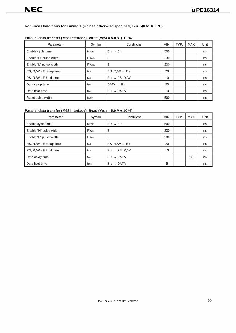
Required Conditions for Timing 1 (Unless otherwise specified, T A = −4−4−4−40 to +85 °°°°C)
Parallel data transfer (M68 interface): Write (V DD1 = 5.0 V ±±±± 10 %)
Parameter Symbol Conditions MIN. TYP. MAX. Unit
Enable cycle time tCYCE E ↑ → E ↑ 500 ns
Enable “H” pulse width PWEH E 230 ns
Enable “L” pulse width PWEL E 230 ns
RS, R,/W - E setup time tAS RS, R,/W → E ↑ 20 ns
RS, R,/W - E hold time tAH E ↓ → RS, R,/W 10 ns
Data setup time tDS DATA → E ↑ 80 ns
Data hold time tDH E ↓ → DATA 10 ns
Reset pulse width tWRE 500 ns
Parallel data transfer (M68 interface): Read (V DD1 = 5.0 V ±±±± 10 %)
Parameter Symbol Conditions MIN. TYP. MAX. Unit
Enable cycle time tCYCE E ↑ → E ↑ 500 ns
Enable “H” pulse width PWEH E 230 ns
Enable “L” pulse width PWEL E 230 ns
RS, R,/W - E setup time tAS RS, R,/W → E ↑ 20 ns
RS, R,/W - E hold time tAH E ↓ → RS, R,/W 10 ns
Data delay time tDD E ↑ → DATA 160 ns
Data hold time tDHR E ↓ → DATA 5 ns
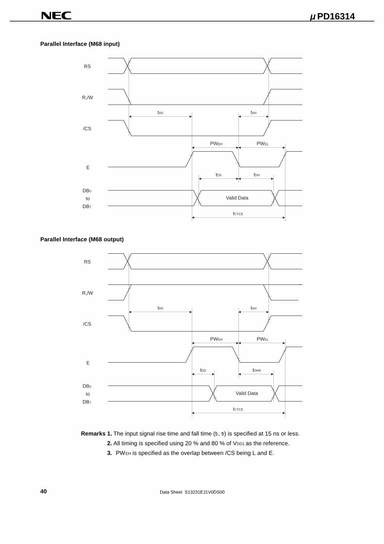
Data Sheet S13231EJ1V0DS0040
µ µ µ µ PD16314
Parallel Interface (M68 input)
RS
R,/W
E
DB0
to
DB7
tAS tAH
PWEH PWEL
tDS tDH
Valid Data
tCYCE
/CS
Parallel Interface (M68 output)
RS
R,/W
E
DB0
to
DB7
tAS tAH
PWEH PWEL
tDD tDHR
Valid Data
tCYCE
/CS
Remarks 1. The input signal rise time and fall time (tr, tf) is specified at 15 ns or less.
2. All timing is specified using 20 % and 80 % of VDD1 as the reference.
3. PWEH is specified as the overlap between /CS being L and E.
Data Sheet S13231EJ1V0DS00 41
µ µ µ µ PD16314
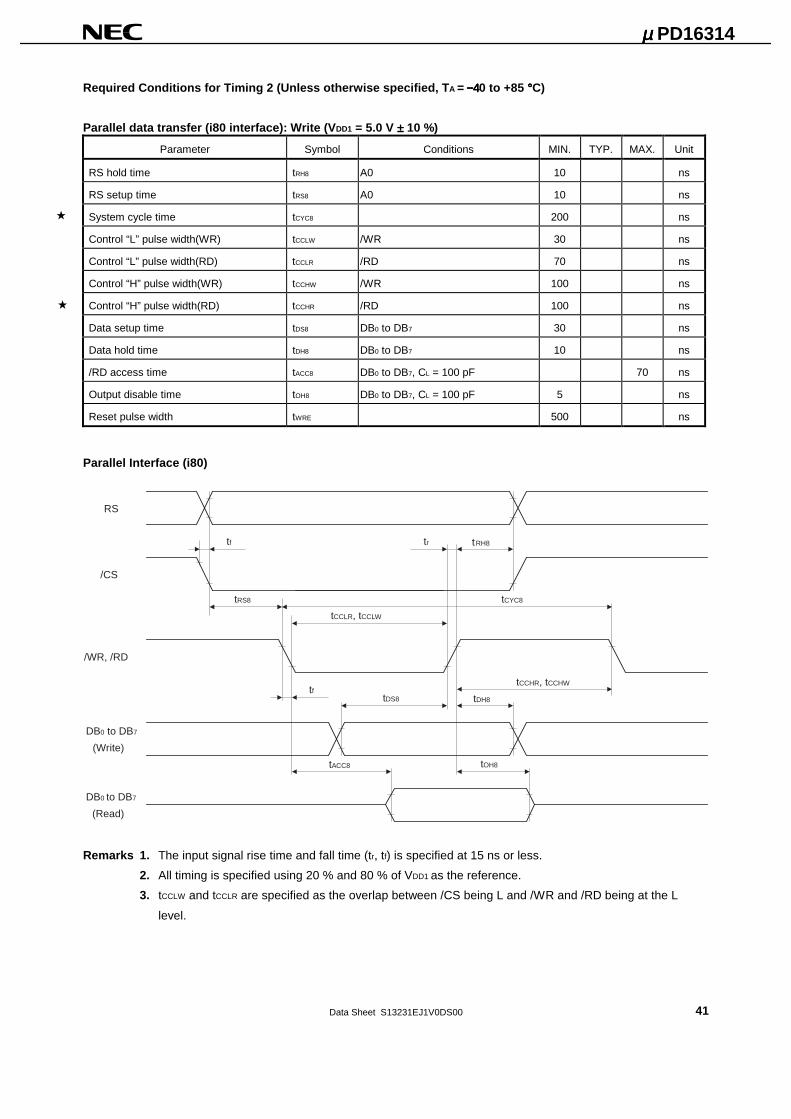
Required Conditions for Timing 2 (Unless otherwise specified, T A = −4−4−4−40 to +85 °°°°C)
Parallel data transfer (i80 interface): Write (V DD1 = 5.0 V ±±±± 10 %)
Parameter Symbol Conditions MIN. TYP. MAX. Unit
RS hold time tRH8 A0 10 ns
RS setup time tRS8 A0 10 ns
System cycle time tCYC8 200 ns
Control “L” pulse width(WR) tCCLW /WR 30 ns
Control “L” pulse width(RD) tCCLR /RD 70 ns
Control “H” pulse width(WR) tCCHW /WR 100 ns
Control “H” pulse width(RD) tCCHR /RD 100 ns
Data setup time tDS8 DB0 to DB7 30 ns
Data hold time tDH8 DB0 to DB7 10 ns
/RD access time tACC8 DB0 to DB7, CL = 100 pF 70 ns
Output disable time tOH8 DB0 to DB7, CL = 100 pF 5 ns
Reset pulse width tWRE 500 ns
Parallel Interface (i80)
tRS8
tRH8
tCCLR, tCCLW
tCYC8
tCCHR, tCCHW
tDH8tDS8
tACC8 tOH8
RS
/CS
/WR, /RD
DB0 to DB7
(Write)
DB0 to DB7
(Read)
tf
trtf
Remarks 1. The input signal rise time and fall time (tr, tf) is specified at 15 ns or less.
2. All timing is specified using 20 % and 80 % of VDD1 as the reference.
3. tCCLW and tCCLR are specified as the overlap between /CS being L and /WR and /RD being at the L
level.

Data Sheet S13231EJ1V0DS0042
µ µ µ µ PD16314
Required Conditions for Timing 3 (Unless otherwise specified, T A = −4−4−4−40 to +85 °°°°C)
Serial data transfer (V DD1 = 5.0 V ±±±± 10 %)
Parameter Symbol Conditions MIN. TYP. MAX. Unit
Shift clock cycle tCYK SCK 500 ns
High-level shift clock pulse width tWHK SCK 200 ns
Low-level shift clock pulse width tWLK SCK 200 ns
Shift clock hold time tHSTBK STB ↓ → SCK ↓ 100 ns
Data setup time tDS DATA → SCK ↑ 100 ns
Data hold time tDH SCK ↑ → DATA 100 ns
STB hold time tDKSTB SCK ↑ → STB ↑ 500 ns
STB pulse width tWSTB 500 ns
Wait time tWAIT 8th CLK ↑ → 1st CLK ↓ 1 µ s
Output data delay time tODD STB ↓ → DATA 150 ns
Output data hold time tODH SCK ↑ → DATA 5 ns
Reset pulse width tWRE 500 ns
Serial Interface (Input)
STB
SCK
SI
tWSTB
tDKSTB
tWLK tWHK
tCYKtHSTBK
tDHtDS
Serial Interface (Output)
STB
SCK
SO
tWSTB
tDKSTB
tWLK tWHK
tCYKtHSTBK
tODHtODD
Remarks 1. The input signal rise time and fall time (tr, tf) is specified at 15 ns or less.
2. All timing is specified using 20 % and 80 % of VDD1 as the reference.
Data Sheet S13231EJ1V0DS00 43
µ µ µ µ PD16314
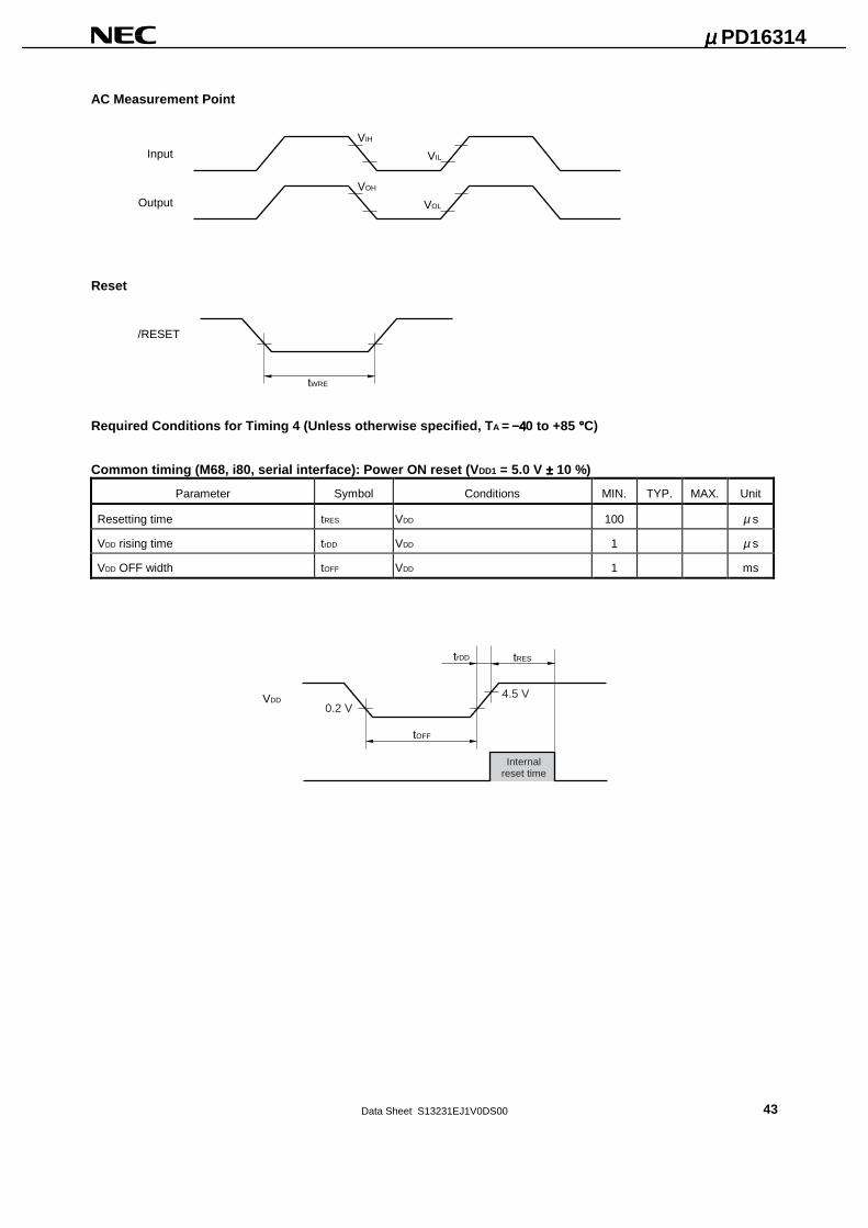
AC Measurement Point
VIH
Input VIL
VOH
Output VOL
Reset
tWRE
/RESET
Required Conditions for Timing 4 (Unless otherwise specified, T A = −4−4−4−40 to +85 °°°°C)
Common timing (M68, i80, serial interface): Power ON reset (V DD1 = 5.0 V ±±±± 10 %)
Parameter Symbol Conditions MIN. TYP. MAX. Unit
Resetting time tRES VDD 100 µ s
VDD rising time trDD VDD 1 µ s
VDD OFF width tOFF VDD 1 ms
tOFF
VDD0.2 V
tREStrDD
4.5 V
Internalreset time

Data Sheet S13231EJ1V0DS0044
µ µ µ µ PD16314
13. PACKAGE DRAWING
144-PIN PLASTIC LQFP (FINE PITCH) (20 20)
ITEM MILLIMETERS INCHESNOTE
Each lead centerline is located within 0.10 mm (0.004 inch) ofits true position (T.P.) at maximum material condition.
A 22.0±0.2 0.866±0.008
B 20.0±0.2 0.787+0.009–0.008
C 20.0±0.2 0.787+0.009–0.008
D
F 1.25
22.0±0.2 0.866±0.008
0.049
S144GJ-50-8EU-2
S 1.7 MAX. 0.067 MAX.
K 1.0±0.2 0.039+0.009–0.008
L 0.5±0.2 0.020+0.008–0.009
R 3 3 +7 –3
+7 –3
G 1.25 0.049
H 0.22 0.009±0.002
I 0.10 0.004
J 0.5 (T.P.) 0.020 (T.P.)
M 0.145 0.006±0.002
N 0.10 0.004
P 1.4±0.1 0.055±0.004
Q 0.125±0.075 0.005±0.003
+0.05–0.04
+0.055–0.045
M
108 73
1 36
109
144
72
37
Detail of lead end
I J
F
G H
QR
P K
M
LN
C D S
A
B
Data Sheet S13231EJ1V0DS00 45
µ µ µ µ PD16314
14. SOLDERING CONDITIONS
Solder the product under the following recommended conditions.
For details of the recommended soldering conditions, refer to information Document Semiconductor Device
Mounting Technology Manual (C10535E).
For soldering methods and soldering conditions other than those recommended, please contact an NEC
salesperson.
Surface Mount Type
µ PD16314GJ-001-8EU: 144-PIN PLASTIC LQFP (20x20 mm)
Soldering
Method
Soldering Condition Symbol of Recommended
Soldering Condition
Infrared reflow Package peak temperature: 235 °C, Time: 30 seconds MAX. (210 °C MIN.),
Number of times: 3 MAX.
<Precaution>
Products other than in heat-resistant trays (such as those packaged in a
magazine, taping, or non-thermal-resistant tray) cannot be baked in their
package.
IR35-103-3
VPS Package peak temperature: 215 °C, Time: 40 seconds MAX. (200 °C MIN.),
Number of times: 3 MAX.
<Precaution>
Products other than in heat-resistant trays (such as those packaged in a
magazine, taping, or non-thermal-resistant tray) cannot be baked in their
package.
VP15-103-3
Wave soldering Solder path temperature: 260 °C MAX., Time: 10 seconds MAX.,
Number of times:1,
Preheating temperature: 120 °C MAX. (Package surface)
WS-60-103-1
Partial heating Pin temperature: 300 °C MAX., Time: 3 seconds MAX. (per side of device) −−−−
Caution Do not use two or more soldering methods in combination (except the partial heating method).

Data Sheet S13231EJ1V0DS0046
µ µ µ µ PD16314
[MEMO]

Data Sheet S13231EJ1V0DS00 47
µ µ µ µ PD16314
NOTES FOR CMOS DEVICES
1 PRECAUTION AGAINST ESD FOR SEMICONDUCTORS
Note:
Strong electric field, when exposed to a MOS device, can cause destruction of the gate oxide and
ultimately degrade the device operation. Steps must be taken to stop generation of static electricity
as much as possible, and quickly dissipate it once, when it has occurred. Environmental control
must be adequate. When it is dry, humidifier should be used. It is recommended to avoid using
insulators that easily build static electricity. Semiconductor devices must be stored and transported
in an anti-static container, static shielding bag or conductive material. All test and measurement
tools including work bench and floor should be grounded. The operator should be grounded using
wrist strap. Semiconductor devices must not be touched with bare hands. Similar precautions need
to be taken for PW boards with semiconductor devices on it.
2 HANDLING OF UNUSED INPUT PINS FOR CMOS
Note:
No connection for CMOS device inputs can be cause of malfunction. If no connection is provided
to the input pins, it is possible that an internal input level may be generated due to noise, etc., hence
causing malfunction. CMOS devices behave differently than Bipolar or NMOS devices. Input levels
of CMOS devices must be fixed high or low by using a pull-up or pull-down circuitry. Each unused
pin should be connected to VDD or GND with a resistor, if it is considered to have a possibility of
being an output pin. All handling related to the unused pins must be judged device by device and
related specifications governing the devices.
3 STATUS BEFORE INITIALIZATION OF MOS DEVICES
Note:
Power-on does not necessarily define initial status of MOS device. Production process of MOS
does not define the initial operation status of the device. Immediately after the power source is
turned ON, the devices with reset function have not yet been initialized. Hence, power-on does
not guarantee out-pin levels, I/O settings or contents of registers. Device is not initialized until the
reset signal is received. Reset operation must be executed immediately after power-on for devices
having reset function.

µ µ µ µ PD16314
• The information in this document is subject to change without notice. Before using this document, please confirm that this is the latest version.• No part of this document may be copied or reproduced in any form or by any means without the prior written consent of NEC Corporation. NEC Corporation assumes no responsibility for any errors which may appear in this document.• NEC Corporation does not assume any liability for infringement of patents, copyrights or other intellectual property rights of third parties by or arising from use of a device described herein or any other liability arising from use of such device. No license, either express, implied or otherwise, is granted under any patents, copyrights or other intellectual property rights of NEC Corporation or others.• Descriptions of circuits, software, and other related information in this document are provided for illustrative purposes in semiconductor product operation and application examples. The incorporation of these circuits, software, and information in the design of the customer's equipment shall be done under the full responsibility of the customer. NEC Corporation assumes no responsibility for any losses incurred by the customer or third parties arising from the use of these circuits, software, and information.• While NEC Corporation has been making continuous effort to enhance the reliability of its semiconductor devices, the possibility of defects cannot be eliminated entirely. To minimize risks of damage or injury to persons or property arising from a defect in an NEC semiconductor device, customers must incorporate sufficient safety measures in its design, such as redundancy, fire-containment, and anti-failure features.• NEC devices are classified into the following three quality grades: "Standard", "Special", and "Specific". The Specific quality grade applies only to devices developed based on a customer designated "quality assurance program" for a specific application. The recommended applications of a device depend on its quality grade, as indicated below. Customers must check the quality grade of each device before using it in a particular application. Standard: Computers, office equipment, communications equipment, test and measurement equipment, audio and visual equipment, home electronic appliances, machine tools, personal electronic equipment and industrial robots Special: Transportation equipment (automobiles, trains, ships, etc.), traffic control systems, anti-disaster systems, anti-crime systems, safety equipment and medical equipment (not specifically designed for life support) Specific: Aircraft, aerospace equipment, submersible repeaters, nuclear reactor control systems, life support systems or medical equipment for life support, etc. The quality grade of NEC devices is "Standard" unless otherwise specified in NEC's Data Sheets or Data Books. If customers intend to use NEC devices for applications other than those specified for Standard quality grade, they should contact an NEC sales representative in advance.
M7 98. 8