
3,350+OPEN ACCESS BOOKS
108,000+INTERNATIONAL
AUTHORS AND EDITORS115+ MILLION
DOWNLOADS
BOOKSDELIVERED TO
151 COUNTRIES
AUTHORS AMONG
TOP 1%MOST CITED SCIENTIST
12.2%AUTHORS AND EDITORS
FROM TOP 500 UNIVERSITIES
Selection of our books indexed in theBook Citation Index in Web of Science™
Core Collection (BKCI)
Chapter from the book Energy Storage in the Emerging Era of Smart GridsDownloaded from: http://www.intechopen.com/books/energy-storage-in-the-emerging-era-of-smart-grids
PUBLISHED BY
World's largest Science,Technology & Medicine
Open Access book publisher
Interested in publishing with IntechOpen?Contact us at [email protected]
5
Lightning Energy: A Lab Scale System
Mohd Farriz Basar, Musa Yusop Lada and Norhaslinda Hasim Universiti Teknikal Malaysia Melaka (UTeM),
Malaysia
1. Introduction
This chapter which has six subchapters explains the energy storage system in harvesting a lightning return stroke for a lab scale system. Nowadays, the world is facing the energy crisis and consequently a renewable energy is required as an energy contributor to solve the crisis. Hence, it is believed that lightning return stroke has a good future to be a free electricity sources. The main difficulty in harnessing the lightning stroke is to attract and simultaneously to store the energy, which limited in a microsecond. Due to that, the computer simulation works using PSpice is done as the preliminary effort intended for the hardware development as well as to understand and verify the proposed system. A lab scale system is set up based on natural characteristics of lightning to determine the performance of the sample capacitor as energy storage accurately. Hence, the single stroke impulse voltage is used as a mock of lightning. Regarding the energy storage device, the capacitor is employed due to the reliability, cost-effective and it is the most common. In addition, the direct tapping system and the high speed switching is most wanted in order to make the whole system more realistic. The capacitors are subjected to 1.2/50μs, 4,200V single-stroke impulse voltages generated by a single stage impulse generator. In this chapter, the energy of impulse voltage that successfully transferred and stored in the storage capacitors is discussed. Basically, the efficiency of the energy transfer is depends on the capacitance values and the switching times. As a final point, the lab scale system explained in this chapter demonstrates the capability to capture the energy from lightning return strokes that can be a clean energy sources. On the other side, lightning which have extremely high current and high voltage is a gratis electricity energy sources that can be replenished. The lab scales systems for harvesting the energy from lightning return stroke, which discussed in this chaper able to give a new contribution to solve the energy crisis and it will be very challenging. Up until now, the mature technology in harvesting the lightning stroke for the large-scale system is still not yet ready and the relevant scientific literature is not easily found. It noted that the final system proposed in this chapter would provide an understanding of the system principle and additionally provide a noteworthy contribution for further research.
2. Clouds and lightning
Lightning return stroke is a complex phenomenon. The large peak currents or the electromagnetic shock wave are capable to kill people and destroy the buildings, trees, animals as well as electrical appliances. As a result, the damage can be outstanding in term of cost.
www.intechopen.com
Energy Storage in the Emerging Era of Smart Grids
90
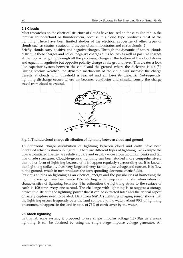
2.1 Clouds Most researches on the electrical structure of clouds have focused on the cumulonimbus, the familiar thundercloud or thunderstorm, because this cloud type produces most of the lightning. There have been limited studies of the electrical properties of other types of clouds such as stratus, stratocumulus, cumulus, nimbostratus and cirrus clouds [2]. Briefly, clouds carry positive and negative charges. Through the dynamic of nature, clouds distribute these charges and collect negative charges at its bottom as well as positive charges at the top. After going through all the processes, charge at the bottom of the cloud draws and equal in magnitude but opposite polarity charge at the ground level. This creates a look like capacitor system between the cloud and the ground where the dielectric is air [3]. During stormy weather, the dynamic mechanism of the cloud will increase the charge density at clouds until threshold is reached and air loses its dielectric. Subsequently, lightning discharge occurs where air becomes conductor and simultaneously the charge travel from cloud to ground.
Fig. 1. Thundercloud charge distribution of lightning between cloud and ground
Thundercloud charge distribution of lightning between cloud and earth have been identified which is shown in Figure 1. There are different types of lightning like example the upward-initiated flashes; are relatively rare and usually occur from mountain peaks and tall man-made structures. Cloud-to-ground lightning has been studied more comprehensively than other form of lightning because of it is happen regularly surrounding us. It is known that lightning strike involves very large and very fast impulse voltage and current. It is flow to the ground, which in turn produces the corresponding electromagnetic fields. Previous studies on lightning as an electrical energy and the possibilities of harnessing the lightning energy have been since 1752 starting with Benjamin Franklin observation on characteristics of lightning behavior. The estimation the lightning strike to the surface of earth is 100 time every one second. The challenge with lightning is to suggest a storage device to distribute the lightning power that it can be extracted later and the critical aspect on safety capture need to be alert. Data from NASA’s lightning imaging sensor shows that the lightning occurs frequently over the land compare to the water. About 90% of lightning phenomenon happens in the land in spite of 75% of earth cover by the water.
2.2 Mock lightning
In this lab scale system, it proposed to use single impulse voltage 1.2/50µs as a mock lightning. It can be obtained by using the single stage impulse voltage generator. An
www.intechopen.com

Lightning Energy: A Lab Scale System
91
impulse voltage is a unidirectional voltage which characterized by two time intervals
expressed in microseconds, µs which is wave front time, tf and wave tail time, tt. Figure 2 shows the impulse voltage waveform that rises rapidly to a maximum value and then decays slowly to zero.
Fig. 2. Standardized impulse voltage wave shape
According to the standard wave shapes, the time to peak value or front time, tf is set to be 1.2µs with the tolerances is ± 30%. Thus, the system proposed must capable to attract and stored the voltage at this peak time. Besides that, the tail time, tt is set to be 50µs with the tolerances is ± 20%. The time to half value of the wave tail of an impulse voltage is the total time occupied by the impulse voltage in rising to peak value and declining there form to half the peak value of the impulse.
3. Energy storage
Energy storage technologies do not represent energy sources, but they provide valuable added benefits to improve power quality, stability and reliability of supply. In this modern power application, practicable storage technologies also known as viable storage technologies like batteries, flywheels, ultra capacitors and superconducting energy storage system was rapidly used. Figure 3 shows a specific energy ranges versus specific power.
Capacitor
Batteries
Flywheel
SMES
1
1000
100
10
0.01 0.1 1 10 100 1000 100000 1000000
Power (MW/g)
En
ergy (
50/3
mW
min
/g)
Fig. 3. Specific power versus specific energy ranges
www.intechopen.com
Energy Storage in the Emerging Era of Smart Grids
92
Optimal Energy System (OES) that consist of flywheel based energy storage system
currently be manufacture and design to provide pulse of energy for charging high voltage
capacitor. This system has been used for electromagnetic air-craft launch system (EMALS)
applications. Flywheel technology has been considered an attractive energy storage choice
due to its potential for reduced weight and volume, high duty-cycle tolerance, and low
maintenance requirements. Flywheel technology overcomes some of the shortcomings of
today’s energy storage systems by having an extremely high cyclic-life, limited temperature
sensitivity, no chemical hazards, charge rate equal to discharge, and reduced weight and
space.
They are a few benefits of adding energy storage to power electronic compensators for
utility application such as improved system reliability, dynamic stability, enhanced power
quality, transmission capacity enhancement and area protection. It shows that energy
storage devices can be integrated to power electronics converters to provide power system
stability, enhanced transmission capability, and improved power quality. Adding energy
storage to power electronics compensators not only enhances the performances of the
device, but can also provide the possibility of reducing the MVA ratings requirements of the
front-end power electronics conversion system. This is an important benefit consideration
when considering adding energy storage systems.
Supercapacitor was an advanced technology as compared to battery or electrostatic
capacitor. The advantage of supercapacitor is high fast step response in term of charge
and discharging. Effects of supercapacitor on power system application are absorbing
high frequency power surges, reduce the degree of discharge and reduce the power
losses.
In order to look into the capability of the lab scale system proposed for harvesting the
lightning energy, two different types of sample capacitor are used. The first type is KNU
1910 Metallized Polypropylene Film Capacitors. The second type is CBB20 Axial-type
Metallized Popypropylene Film Capacitor. These two types of sample capacitor used same
dielectric, which is polypropylene film. The polypropylene capacitor was selected to be used
in the testing because it is cheap, high temperature stability, readily available and it is
widely used in high frequency, DC and pulse circuit’s applications.
Many polypropylene film capacitors have a tolerance about 5% to 10%, which is adequate
for many applications. In addition, there is very little change in capacitance when these
capacitors are used in applications within frequency range of 100,000Hz. Moreover, the
electrodes are vacuum evaporated metal on dielectric. So, the possibility for bad contact
during the operation of capacitors is excluded. It also has a long life due to self-healing effect
and suitable for high current.
4. High speed switching
As discussed in subchapter 2.2, the maximum value of the impulse voltage is occurred at
1.2µs. Consequently, the system proposed must able to draw out and store the energy of the
impulse voltage (mock lightning) particularly at that extremely short time. Hence, the high
speed switching is imperative to isolate the sample capacitor from any connection once the
energy enters the sample capacitor. As a result, the potential voltage that can be retained or
sustained in the sample capacitor can be investigate.
www.intechopen.com

Lightning Energy: A Lab Scale System
93
Figure 4 shows the block diagram of the high speed switching circuit that is used in the
experimental work. The high speed switching controller consists of a microcontroller, a gate
drive and a switching device and the orientation of components is shown in Figure 5.
MICRO
CONTROLLER
IMPULSE
VOLTAGE
(Mock Lightning)
CAPACITOR
(Energy Storage) SWITCHING
DEVICE
GATE
DRIVE
SWITCH CONTROLLER
Fig. 4. Block diagram of the high speed switching circuit
4.1 High speed switching components The advantages of this switching circuit are the circuit is simple and the cost is low. The main components that are used in the circuit are indicated in the Table 1. The high voltage IGBT is preferred to use as a switching device because it has a tremendous performance and widely used. The type of IGBT that be used are NPT (Non Punch Through) type, which is low efficient emitter and high carrier lifetime compare to others types of IGBT.
Components Description
Micro Controller PIC 16F84A
• It is a peripheral interface controller
• 16 series PIC, 14 bit (instructions)
microcontroller
• Maximum operating frequency is
20MHz
Gate Drive NPN Transistor
• Part Number : BC548B
• Manufacturer : Fairchild
Semiconductor
Switching Device High Voltage IGBT • Part Number : IXGR 16N170AH1
• Manufacturer : IXYS
Table 1. Main components of switching controller
The micro controller circuit and gate drive requires 5Vdc of supply whilst the high voltage
IGBT (switching device) requires 15Vdc to turn ON and 0Vdc to turn OFF as illustrated in
Figure 6. Meanwhile, in Figure 7, to activate the switching circuit, two different level of
voltage supply is required. The micro controller circuit and the gate drive requires 5Vdc of
supply whilst the high voltage IGBT (switching device) requires 12Vdc.
It can see that there has an 4,200V impulse voltage at the right side of the circuit in Figure 7.
At the beginning, the IGBT switch is in close position. Ideally, when the charges from the
impulse voltage go into the capacitor, the IGBT switch will be open in order to isolate the
capacitor to discharge. With the aid of IGBT switch, now the capacitor is like a battery.
www.intechopen.com

Energy Storage in the Emerging Era of Smart Grids
94
Fig. 5. Orientation of components of high speed switching controller
Vgg RgVgs
Vaa
C
Vgon
ton toff
Fig. 6. Circuit diagram of IGBT with signal turn ON and OFF
D7 LED RED
R9 1k
R8 1k
X1
20MEG C
3 30pF
C4 30pF
U3
16F84A
1
57
11
10
15 16
4
2
8
RA2
VSS
RB1
RB5
RB4
CLKOUT CLKIN
RESET
RA3
RB2
RELAY R10
1k
IGBT
R7 1k
R6 1k
R5 1k
RESET
SW2
SW1
V1
5V D
6 LED GREEN
V2
5V
V3 12V
Q1
BC548B
Sample Capacitor
V4 4200
V C
G
E
Fig. 7. Schematic diagram of the high speed switching circuit
www.intechopen.com

Lightning Energy: A Lab Scale System
95
4.2 Peripheral interface controller (PIC16F84A) PIC is an abbreviation for Peripheral Interface Controller. It is not PLC or Programmable Logic Controller as most misunderstood, because it is an integrated chip (IC) based controller. When IC based controller is concerned, the logic levels, 0 and 1 are 0 volt and 5 volt respectively. PIC is one of the micro technology generation and even more popular in industrial and hobbyists causing by the advantage on using it. Some of the advantage of PIC is low cost, widely available, large user base, extensive application, and serial programming capability which is the programming data of HEX (PIC data) can be write and re-write this is because PIC is made from flash memory. A microcontroller is normally used for simple applications such as washing machines, rice cooker, air conditioner, keyboards, mouse, Liquid Crystal Displays (LCD) and much more. This means that the microcontroller is used for small applications and sometimes for standalone systems. PIC is a brand of microcontroller, from its manufacturer, Microchip. The decision to use the PIC in this project is due to the vast employ of this device in many applications. It has Reduced Instruction Set Computer (RISC) architecture and moreover the assembly program is much simpler rather than other brands, such as Freescale (Motorola), Intel and many others. However, for the lab scale system proposed in this chapter used PIC16F84A as shown in Figure 8. Table 2 shows the function for every pin of PIC16F84A.
Fig. 8. Pin diagram for PIC16F84A
For programming, C language is used to write the program. Then compiler software is required to convert the C language to machine language (in zeros and ones). The compilers that have been used is mikroC. Next when the machine languages are generated, a downloader is required. The functions of this software is to transfer the machine codes of the program along with the settings to the PIC 16F84A. In simple words, the software installs the PIC with the machine codes of the program. In this project, WINPIC800 software is used because one of its advantages is that it can detect the type of PIC inserted automatically.
5. Computer simulation works
This section discuss about the computer simulation works using Pspice software. The purpose of the simulation is to obtain the testing circuit configuration that needs to be used in the experimental work. Moreover, the results of the computer simulation will verify the effort to harvest the lightning impulse voltage.
www.intechopen.com
Energy Storage in the Emerging Era of Smart Grids
96
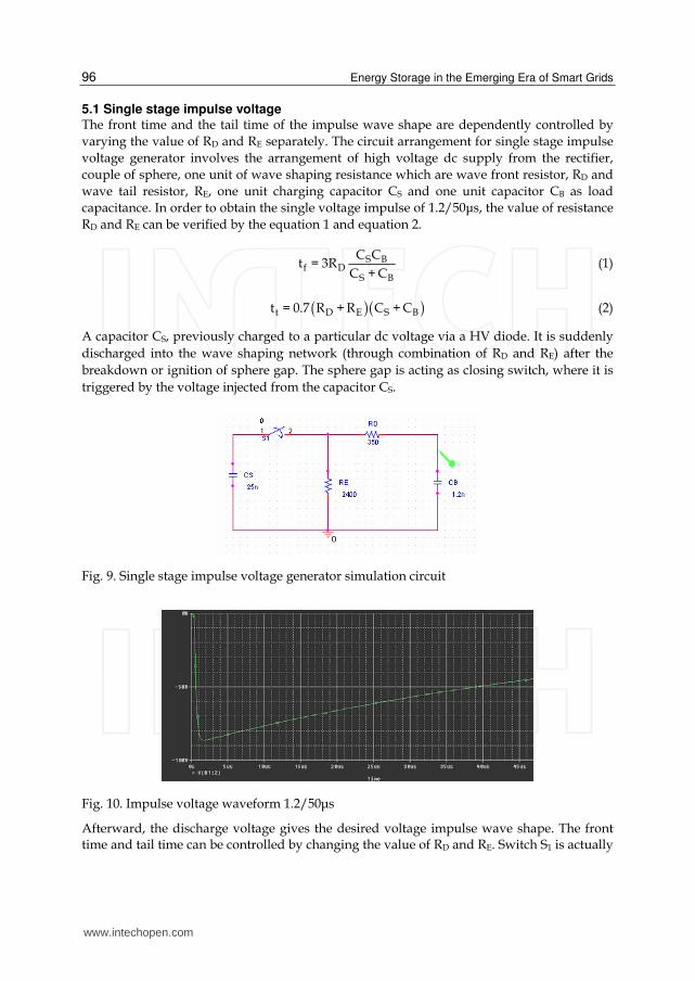
5.1 Single stage impulse voltage The front time and the tail time of the impulse wave shape are dependently controlled by
varying the value of RD and RE separately. The circuit arrangement for single stage impulse
voltage generator involves the arrangement of high voltage dc supply from the rectifier,
couple of sphere, one unit of wave shaping resistance which are wave front resistor, RD and
wave tail resistor, RE, one unit charging capacitor CS and one unit capacitor CB as load
capacitance. In order to obtain the single voltage impulse of 1.2/50μs, the value of resistance
RD and RE can be verified by the equation 1 and equation 2.
S Bf D
S B
C Ct = 3R
C + C (1)
( )( )t D E S Bt = 0.7 R + R C + C (2)
A capacitor CS, previously charged to a particular dc voltage via a HV diode. It is suddenly
discharged into the wave shaping network (through combination of RD and RE) after the
breakdown or ignition of sphere gap. The sphere gap is acting as closing switch, where it is
triggered by the voltage injected from the capacitor CS.
Fig. 9. Single stage impulse voltage generator simulation circuit
Fig. 10. Impulse voltage waveform 1.2/50μs
Afterward, the discharge voltage gives the desired voltage impulse wave shape. The front time and tail time can be controlled by changing the value of RD and RE. Switch S1 is actually
www.intechopen.com
Lightning Energy: A Lab Scale System
97
a sphere gap. The rapid rise and slow decay impulse voltage wave shape can be generated by the activities of charging and discharging circuits with two energy storage elements, which are CS and CB. The CB will be the capacitance of insulation to be tested or known as a load. As shown in Figure 9, it can see that CS>>CB and RD>>RE. Theoritically, the impulse voltage wave shape is composed by the superposition of two exponential functions. As mentioned before, the charging capacitor CS is charged via a high voltage dc supply through the rectifier. In the simulation, the initial condition for CS is set to 8,600V and then it is discharged by closing switch S1 (sparks in the sphere gap). Then, the simulation result is taken from the voltage across the load capacitor CB. The simulation result in Figure 10 shows that, the peak impulse voltage is 8,600V with the front time tf of 1.5μs and the tail time tt of 47μs.
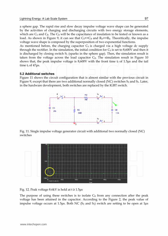
5.2 Additional switches Figure 11 shows the circuit configuration that is almost similar with the previous circuit in Figure 9, except that there are two additional normally closed (NC) switches S2 and S3. Later, in the hardware development, both switches are replaced by the IGBT switch.
Fig. 11. Single impulse voltage generator circuit with additional two normally closed (NC) switches
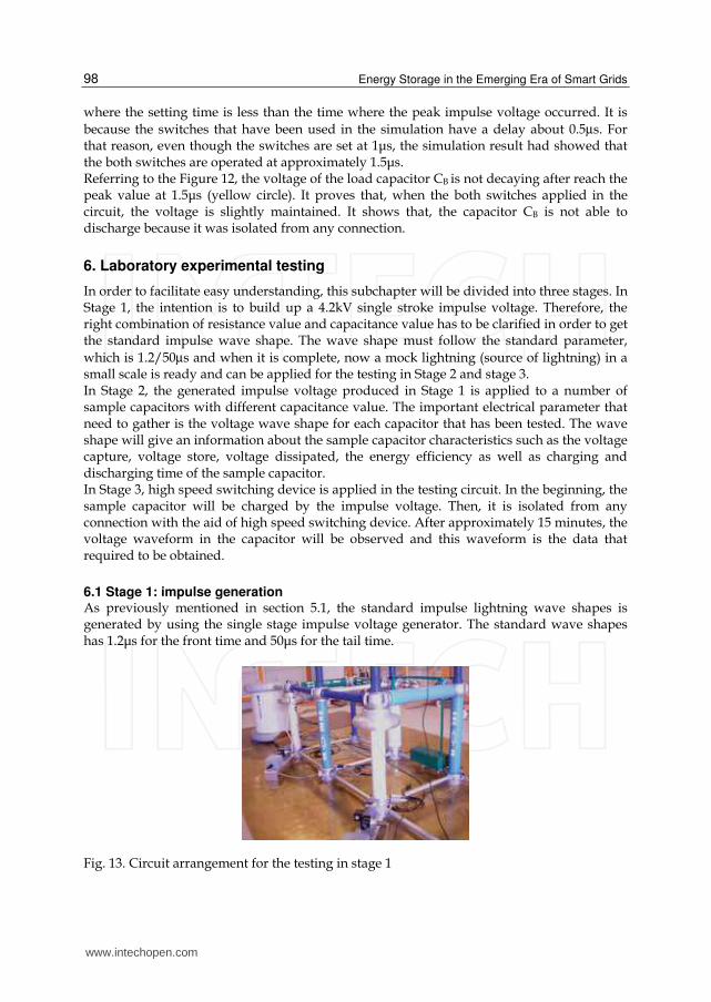
Fig. 12. Peak voltage 8.6kV is hold at t ≥ 1.5μs
The purpose of using these switches is to isolate CB from any connection after the peak voltage has been attained in the capacitor. According to the Figure 2, the peak value of
impulse voltage occurs at 1.5μs. Both NC (S2 and S3) switch are setting to be open at 1µs
www.intechopen.com
Energy Storage in the Emerging Era of Smart Grids
98
where the setting time is less than the time where the peak impulse voltage occurred. It is
because the switches that have been used in the simulation have a delay about 0.5µs. For that reason, even though the switches are set at 1μs, the simulation result had showed that the both switches are operated at approximately 1.5μs. Referring to the Figure 12, the voltage of the load capacitor CB is not decaying after reach the peak value at 1.5μs (yellow circle). It proves that, when the both switches applied in the circuit, the voltage is slightly maintained. It shows that, the capacitor CB is not able to discharge because it was isolated from any connection.
6. Laboratory experimental testing
In order to facilitate easy understanding, this subchapter will be divided into three stages. In Stage 1, the intention is to build up a 4.2kV single stroke impulse voltage. Therefore, the right combination of resistance value and capacitance value has to be clarified in order to get the standard impulse wave shape. The wave shape must follow the standard parameter,
which is 1.2/50µs and when it is complete, now a mock lightning (source of lightning) in a small scale is ready and can be applied for the testing in Stage 2 and stage 3. In Stage 2, the generated impulse voltage produced in Stage 1 is applied to a number of sample capacitors with different capacitance value. The important electrical parameter that need to gather is the voltage wave shape for each capacitor that has been tested. The wave shape will give an information about the sample capacitor characteristics such as the voltage capture, voltage store, voltage dissipated, the energy efficiency as well as charging and discharging time of the sample capacitor. In Stage 3, high speed switching device is applied in the testing circuit. In the beginning, the sample capacitor will be charged by the impulse voltage. Then, it is isolated from any connection with the aid of high speed switching device. After approximately 15 minutes, the voltage waveform in the capacitor will be observed and this waveform is the data that required to be obtained.
6.1 Stage 1: impulse generation As previously mentioned in section 5.1, the standard impulse lightning wave shapes is generated by using the single stage impulse voltage generator. The standard wave shapes has 1.2μs for the front time and 50μs for the tail time.
Fig. 13. Circuit arrangement for the testing in stage 1
www.intechopen.com

Lightning Energy: A Lab Scale System
99
The equipments that need to be used to setup the single impulse generator as shown in Figure 13 are consisted of Single Phase AC Voltage Test Transformer, HV rectifier, charging and load capacitor, wave shaping resistance, sphere gap, grounding rod, voltage divider, HV probe and oscilloscope.
CS 25nF
RE
2400 Ω
RD 355 Ω
470nF
CB 1.19 nF
1200pF
Oscilloscope
Fig. 14. Circuit diagram for stage 1 testing
By using the single stage impulse voltage generator circuit arrangement as shown in Figure 14, the desired impulse voltage wave shape has been achieved by choosing the correct
resistance values for RD and RE as well as the capacitance values for CS and CB. In order to verify the impulse wave shape parameters, a digital oscilloscope is used to capture the experimental impulse voltage wave shapes with conjunction with the voltage divider. Besides that, the value of CS, CB, RD and RE are fixed in order to get a sustained 1.2/50μs
wave shape. This is because the testing in the stage 2 and stage 3 will use the same magnitude of impulse voltage.
6.1.1 Front time, tail time and peak voltage of the experimental wave shape Table 2 shows the right combination of the capacitance and resistance value for CS, CB, RD
and RE that connected as shown in Figure 13 and Fiure 14. In order to obtain the resistance
and capacitance value, equation (1) and equation (2) in section 5.1 is used. As a result, the
front time tf and tail time tt for the generated impulse voltage are 1.3μs and 45μs
respectively. This value is slightly different from the standard impulse wave shape.
However, it is accepted for the reason that the experimental value is still under the tolerance
of impulse wave shape parameter, which is +8.3% for the tf and −10% for the tt.
Standard Impulse Voltage Waveshape 1.2/50μs
Value of charging capacitance, CS 25 nF
Value of load capacitance, CB 1.19 nF
Value of resistance, RD 355 Ω
Value of resistance, RE 2400 Ω
Front Time, tf simulation 1.51 μs
Tail Time, tt simulation 47.0 μs
Front Time, tf calculation 1.21 μs
Tail Time, tt calculation 44.0 μs
Front Time, tf experimental 1.30 μs
Tail Time, tt experimental 45.0 μs
Table 2. Value of CS, CB, RD and RE that was used to obtain the standard impulse
www.intechopen.com
Energy Storage in the Emerging Era of Smart Grids
100
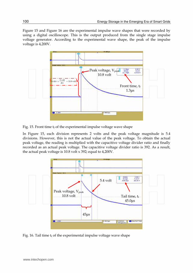
Figure 15 and Figure 16 are the experimental impulse wave shapes that were recorded by using a digital oscilloscope. This is the output produced from the single stage impulse voltage generator. According to the experimental wave shape, the peak of the impulse voltage is 4,200V.
Fig. 15. Front time tf of the experimental impulse voltage wave shape
In Figure 15, each division represents 2 volts and the peak voltage magnitude is 5.4 divisions. However, this is not the actual value of the peak voltage. To obtain the actual peak voltage, the reading is multiplied with the capacitive voltage divider ratio and finally recorded as an actual peak voltage. The capacitive voltage divider ratio is 392. As a result, the actual peak voltage is 10.8 volt x 392; equal to 4,200V.
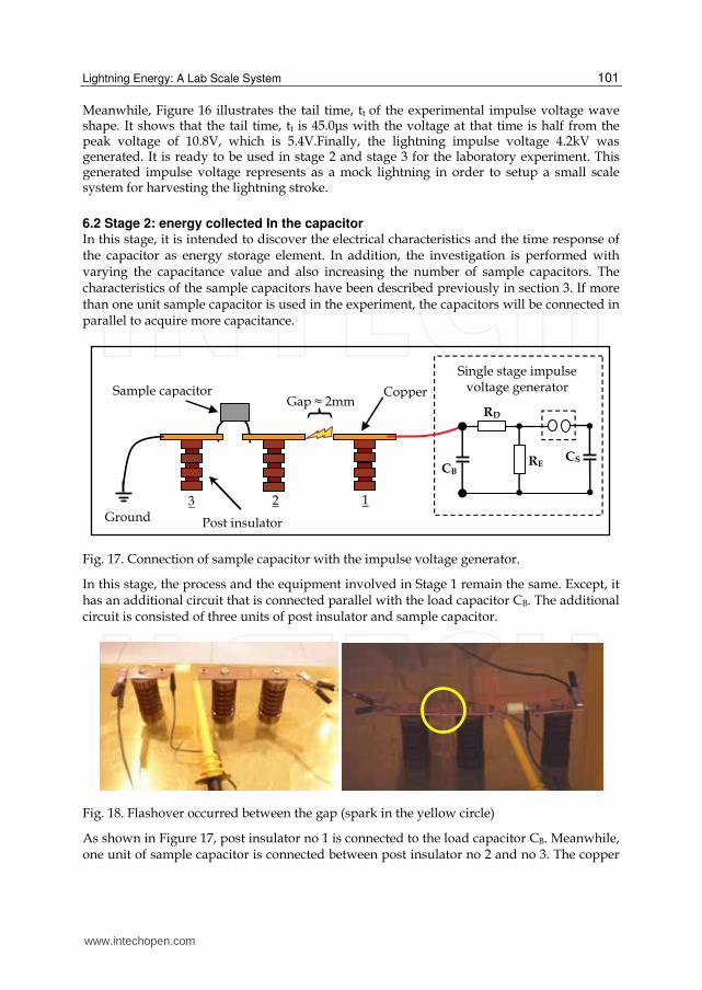
Fig. 16. Tail time tt of the experimental impulse voltage wave shape
Tail time, tt
45.0μs
Peak voltage, Vpeak
10.8 volt
5.4 volt
45μs
2 volt5.4 div x 10.8 volt
div=
Front time, tf
1.3μs
Peak voltage, Vpeak 10.8 volt
www.intechopen.com
Lightning Energy: A Lab Scale System
101
Meanwhile, Figure 16 illustrates the tail time, tt of the experimental impulse voltage wave shape. It shows that the tail time, tt is 45.0μs with the voltage at that time is half from the peak voltage of 10.8V, which is 5.4V.Finally, the lightning impulse voltage 4.2kV was generated. It is ready to be used in stage 2 and stage 3 for the laboratory experiment. This generated impulse voltage represents as a mock lightning in order to setup a small scale system for harvesting the lightning stroke.
6.2 Stage 2: energy collected In the capacitor In this stage, it is intended to discover the electrical characteristics and the time response of the capacitor as energy storage element. In addition, the investigation is performed with varying the capacitance value and also increasing the number of sample capacitors. The characteristics of the sample capacitors have been described previously in section 3. If more than one unit sample capacitor is used in the experiment, the capacitors will be connected in parallel to acquire more capacitance.
Post insulator
Gap ≈ 2mm Sample capacitor
Ground
Copper
CB RE CS
RD
3 2 1
Single stage impulse voltage generator
Fig. 17. Connection of sample capacitor with the impulse voltage generator.
In this stage, the process and the equipment involved in Stage 1 remain the same. Except, it has an additional circuit that is connected parallel with the load capacitor CB. The additional circuit is consisted of three units of post insulator and sample capacitor.
Fig. 18. Flashover occurred between the gap (spark in the yellow circle)
As shown in Figure 17, post insulator no 1 is connected to the load capacitor CB. Meanwhile, one unit of sample capacitor is connected between post insulator no 2 and no 3. The copper
www.intechopen.com

Energy Storage in the Emerging Era of Smart Grids
102
bar at the post insulator no 1 and no 2 is not connected and it has a gap about 2mm. At the time when flashover occurs as shown in Figure 18, the gap will act as a closing switch and simultaneously completed the circuit and charging the sample capacitor. Throughout all these processes, the electrical characteristics and the time response of the sample capacitor can be obtained and measured via HV probe.
Fig. 19. Decaying time for one unit sample capacitor 0.22 μF
The detailed information regarding the decaying period for one unit capacitor 0.22uF
(KNU1910) is illustrated in Figure 19. The decaying time from the peak voltage to the zero
voltage is 93 seconds. After the data collection for the peak voltage, rising time and the
decaying of one unit capacitor is completed, the process will be continued for two units as
well as three units of capacitors connected in parallel.
In order to achieve a clearer picture regarding the voltage efficiency and dissipated voltage for
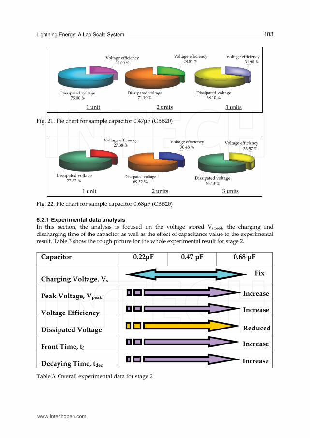
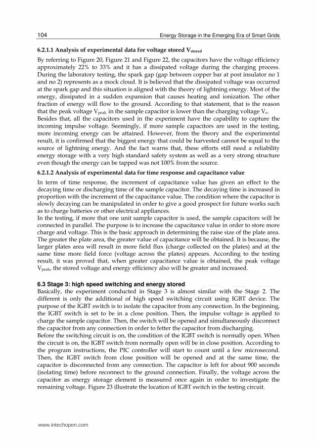
all the sample capacitors used in the laboratory experiment, Figure 20, Figure 21 and Figure 22
can be used as references. In these figures, the pie charts illustrate the relationship between
voltage and voltage efficiency for one unit, two units and three units of sample capacitor. It
proves that the voltage efficiency has an inverse relation with the dissipated voltage, that is
when the voltage efficiency increased, the voltage dissipated will be reduced and vice versa.
Dissipated
voltage
77%
Voltage
efficiency
23%
Dissipated
voltage
72%
Dissipated
voltage
74%
Voltage
efficiency
26%
1 unit
Voltage efficiency 25.71 %
2 units 3 units
Voltage efficiency 22.62 %
Dissipated voltage 77.38 %
Dissipated voltage 74.29 %
Dissipated voltage 71.67 %
Voltage efficiency
28.35%
Fig. 20. Pie chart for sample capacitor 0.22μF (KNU 1910)
Peak voltage, Vpeak 950 volt
Decaying time (discharging), tdec 93 s
Decaying time, tdec 93 s
www.intechopen.com
Lightning Energy: A Lab Scale System
103
Voltage
efficiency
25%
Dissipated
voltage
75%
Dissipated
voltage
71%
Voltage
efficiency
29%
Dissipated
voltage
68%
Voltage
efficiency
32%
1 unit 2 units 3 units
Voltage efficiency 25.00 %
Voltage efficiency 28.81 %
Voltage efficiency31.90 %
Dissipated voltage 75.00 %
Dissipated voltage 68.10 %
Dissipated voltage 71.19 %
Fig. 21. Pie chart for sample capacitor 0.47μF (CBB20)
Dissipated
voltage
73%
Voltage
efficiency
27%
Voltage
efficiency
30%
Dissipated
voltage
70%
Dissipated
voltage
66%
Voltage
efficiency
34%
1 unit
Dissipated voltage 72.62 %
Dissipated voltage
69.52 % Dissipated voltage
66.43 %
2 units 3 units
Voltage efficiency 27.38 %
Voltage efficiency 30.48 %
Voltage efficiency
33.57 %
Fig. 22. Pie chart for sample capacitor 0.68μF (CBB20)
6.2.1 Experimental data analysis In this section, the analysis is focused on the voltage stored Vstored, the charging and discharging time of the capacitor as well as the effect of capacitance value to the experimental result. Table 3 show the rough picture for the whole experimental result for stage 2.
Capacitor 0.22μF 0.47 μF 0.68 μF
Charging Voltage, Vs
Peak Voltage, Vpeak
Voltage Efficiency
Dissipated Voltage
Front Time, tf
Decaying Time, tdec
Fix
Increase
Increase
Increase
Increase
Reduced
Table 3. Overall experimental data for stage 2
www.intechopen.com
Energy Storage in the Emerging Era of Smart Grids
104
6.2.1.1 Analysis of experimental data for voltage stored Vstored
By referring to Figure 20, Figure 21 and Figure 22, the capacitors have the voltage efficiency approximately 22% to 33% and it has a dissipated voltage during the charging process. During the laboratory testing, the spark gap (gap between copper bar at post insulator no 1 and no 2) represents as a mock cloud. It is believed that the dissipated voltage was occurred at the spark gap and this situation is aligned with the theory of lightning energy. Most of the energy, dissipated in a sudden expansion that causes heating and ionization. The other fraction of energy will flow to the ground. According to that statement, that is the reason that the peak voltage Vpeak in the sample capacitor is lower than the charging voltage Vs. Besides that, all the capacitors used in the experiment have the capability to capture the incoming impulse voltage. Seemingly, if more sample capacitors are used in the testing, more incoming energy can be attained. However, from the theory and the experimental result, it is confirmed that the biggest energy that could be harvested cannot be equal to the source of lightning energy. And the fact warns that, these efforts still need a reliability energy storage with a very high standard safety system as well as a very strong structure even though the energy can be tapped was not 100% from the source.
6.2.1.2 Analysis of experimental data for time response and capacitance value
In term of time response, the increment of capacitance value has given an effect to the decaying time or discharging time of the sample capacitor. The decaying time is increased in proportion with the increment of the capacitance value. The condition where the capacitor is slowly decaying can be manipulated in order to give a good prospect for future works such as to charge batteries or other electrical appliances. In the testing, if more that one unit sample capacitor is used, the sample capacitors will be connected in parallel. The purpose is to increase the capacitance value in order to store more charge and voltage. This is the basic approach in determining the raise size of the plate area. The greater the plate area, the greater value of capacitance will be obtained. It is because, the larger plates area will result in more field flux (charge collected on the plates) and at the same time more field force (voltage across the plates) appears. According to the testing result, it was proved that, when greater capacitance value is obtained, the peak voltage Vpeak, the stored voltage and energy efficiency also will be greater and increased.
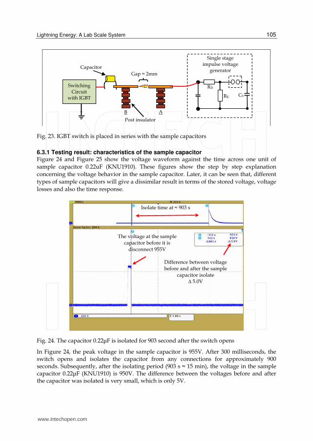
6.3 Stage 3: high speed switching and energy stored Basically, the experiment conducted in Stage 3 is almost similar with the Stage 2. The different is only the additional of high speed switching circuit using IGBT device. The purpose of the IGBT switch is to isolate the capacitor from any connection. In the beginning, the IGBT switch is set to be in a close position. Then, the impulse voltage is applied to charge the sample capacitor. Then, the switch will be opened and simultaneously disconnect the capacitor from any connection in order to fetter the capacitor from discharging. Before the switching circuit is on, the condition of the IGBT switch is normally open. When the circuit is on, the IGBT switch from normally open will be in close position. According to the program instructions, the PIC controller will start to count until a few microsecond. Then, the IGBT switch from close position will be opened and at the same time, the capacitor is disconnected from any connection. The capacitor is left for about 900 seconds (isolating time) before reconnect to the ground connection. Finally, the voltage across the capacitor as energy storage element is measured once again in order to investigate the remaining voltage. Figure 23 illustrate the location of IGBT switch in the testing circuit.
www.intechopen.com
Lightning Energy: A Lab Scale System
105
RE CS
RD
Single stage impulse voltage
generator
Post insulator
Gap ≈ 2mm
Capacitor
B A
Switching Circuit
with IGBT
Fig. 23. IGBT switch is placed in series with the sample capacitors
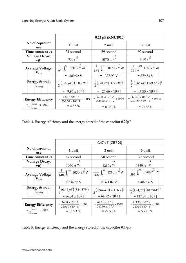
6.3.1 Testing result: characteristics of the sample capacitor Figure 24 and Figure 25 show the voltage waveform against the time across one unit of
sample capacitor 0.22uF (KNU1910). These figures show the step by step explanation
concerning the voltage behavior in the sample capacitor. Later, it can be seen that, different
types of sample capacitors will give a dissimilar result in terms of the stored voltage, voltage
losses and also the time response.
Fig. 24. The capacitor 0.22μF is isolated for 903 second after the switch opens
In Figure 24, the peak voltage in the sample capacitor is 955V. After 300 milliseconds, the switch opens and isolates the capacitor from any connections for approximately 900 seconds. Subsequently, after the isolating period (903 s ≈ 15 min), the voltage in the sample capacitor 0.22μF (KNU1910) is 950V. The difference between the voltages before and after the capacitor was isolated is very small, which is only 5V.
Isolate time at ≈ 903 s
The voltage at the sample capacitor before it is
disconnect 955V
Difference between voltage before and after the sample
capacitor isolate
∆ 5.0V
www.intechopen.com

Energy Storage in the Emerging Era of Smart Grids
106
Fig. 25. Voltage waveform of the sample capacitor after isolating period.
Moreover, Figure 25 shows the voltage waveform after the isolating period where the
sample capacitor 0.22uF (KNU1910) was reconnected with the ground connection. This
figure illustrates that the decaying time is 87 second. The difference in terms of decaying
time between stage 2 and stage 3 does not have much difference, where the discharging time
for the stage 2 is 91 second and for stage 3 is 87 second.
However, the performance of the capacitor 0.46uF (CBB20) and 0.68uF (CBB20) was not as
good as the capacitor 0.22uF (KNU1910). Both capacitors have no capability to retain and
sustain the voltage during the isolating period. Besides that, there was a huge difference
between the decaying time for stage 2 and stage 3.
6.3.2 Experimental data analysis Table 4, Table 5 and Table 6 shows the step by step calculation in determining the energy
stored and the energy efficiency of the sample capacitor. Thus, determining the decaying
voltage function v(t) for every sample capacitor will be the basic step for the energy
calculations. Once, the decaying voltage function v(t) is obtained, it will be used to calculate
the average voltage Vave, the energy stored Estored and the energy efficiency Eefficiency of the
sample capacitor.
Throughout the testing in stage 3, the source voltage Vsource is fixed at 4.2kV. It means that,
the energy supplied by the impulse voltage generator to the sample capacitor is
maintained. Herewith is the calculation for the energy supplied from the impulse voltage
generator.
( ) ( )22
S s sEnergy source, E 0.5 C V 0.5 2500 pF 4200V 0.2205 Joule= = =
After isolate the capacitor for ≈ 900s, the voltage is 950V
Decaying time, tdec 89s
Decaying time, tdec ≈ 89 s
Voltage across the capacitor after isolated
950 V
www.intechopen.com
Lightning Energy: A Lab Scale System
107
0.22 μF (KNU1910)
No of capacitor use
1 unit 2 unit 3 unit
Time constant , τ 31 second 59 second 92 second
Voltage Decay, v(t)
31950
t
e
−
591070
t
e
−
921180
t
e
−
Average Voltage, Vave
= 300.92 V
= 327.93 V
= 379.53 V
Energy Stored, Estored
= 9.96 x 10⁻³ J
= 23.66 x 10⁻³ J
= 47.53 x 10⁻³ J
Energy Efficiency
%1001050.220
1096.9
3
3
xJx
Jx
−
−
=
= 4.52 %
= 10.73 %
= 21.55%
Table 4. Energy efficiency and the energy stored of the capacitor 0.22μF
0.47 μF (CBB20)
No of capacitor use
1 unit 2 unit 3 unit
Time constant , τ 47 second 90 second 126 second
Voltage Decay, v(t)
Average Voltage, Vave
= 334.57 V
= 371.07 V
= 407.96 V
Energy Stored, Estored
= 26.31 x 10⁻³ J
= 64.72 x 10⁻³ J
= 117.33 x 10⁻³ J
Energy Efficiency
%1001050.220
1031.26
3
3
xJx
Jx
−
−
=
= 11.93 %
%1001050.220
1072.64
3
3
xJx
Jx
−
−
=
= 29.53 %
%1001050.220
1033.117
3
3
xJx
Jx
−
−
=
= 53.21 %
Table 5. Energy efficiency and the energy stored of the capacitor 0.47μF
( ) ( )2
92.30022.02
1VFµ ( ) ( )2
93.32744.02
1VFµ ( ) ( )2
53.37966.02
1VFµ
dte
t
3193
0
95093
1−∫ dte
t
59184
0
1070184
1−∫ dte
t
92271
0
1180271
1−∫
100%xE
E
source
stored=
%1001050.220
1066.23
3
3
xJx
Jx
−
−
= %1001050.220
1053.47
3
3
xJx
Jx
−
−
=
100%xE
E
source
stored=
( ) ( )2
07.37194.02
1VFµ ( ) ( )2
96.40741.12
1VFµ
90
t
e1050
−
90
t
e1210
−
126
t
e1340
−
dte
t
47140
0
1050140
1−∫ dte
t
90268
0
1210268
1−∫ dte
t
126396
0
1340396
1−∫
( ) ( )2
57.33447.02
1VFµ
www.intechopen.com

Energy Storage in the Emerging Era of Smart Grids
108
0.68 μF (CBB20)
No of capacitor use
1 unit 2 unit 3 unit
Time constant , τ 68 second 121 second 171 second
Voltage Decay, v(t)
Average Voltage, Vave
= 362.75 V
= 385.59 V
= 410.45 V
Energy Stored, Estored
= 44.74 x 10⁻³ J
= 101.10 x 10⁻³ J
= 171.83 x 10⁻³ J
Energy Efficiency
%1001050.220
1074.44
3
3
xJx
Jx
−
−
=
= 20.29 %
%1001050.220
1010.101
3
3
xJx
Jx
−
−
=
= 45.85 %
%1001050.220
1083.171
3
3
xJx
Jx
−
−
=
= 77.93%
Table 6. Energy efficiency and the energy stored of the capacitor 0.68μF
6.3.3 Analysis of experimental data for voltage stored and energy efficiency As mentioned before, the energy supplied by the lightning impulse voltage generator is maintained at approximately 0.2205 Joule. According to Table 4, Table 5 and Table 6, the measurement data shows that the capacitors used in the testing have the energy efficiency in the range of 4.52% to 77.93%. The data also proved that the energy efficiency increases together with the increment of capacitance value. Instead of the capacitance value, there are a few factors that will give a significance effect to the voltage stored as well as the energy efficiency. One of the factors is the type of capacitor that was used in the experiments. It knows that, the energy efficiency is proportional with the stored voltage. From the measurement result, only the capacitor 0.22μF (KNU1910) is capable of sustaining the voltage compared to other sample capacitors. In other words, even though the energy efficiency for this capacitor is lower from other sample capacitor, only a small voltage losses occurred. The opposite of that, the sample capacitors 0.47μF (CBB20) and 0.68μF (CBB20) suffer a huge voltage losses during the isolating period. It means that, there will be sometime when the voltage stored in both these capacitor reduces to the zero voltage and causes a zero energy efficiency. Another factor that is responsible in obtaining the higher energy efficiency is the tapping method. It is because, the tapping system will be the primary role to attract and capture the lighting energy. It means that, this part have to captured as much as the energy supplied and also transfer the energy to the storage devices. The last factor is the effectiveness of the high speed switching device. The main task of this switching device is to facilitate the capacitors to sustain the charge and the voltage during the separating period. By referring to the measurement data, the high speed switching applied in the testing circuit gave a good performance.
7. Discussion and conclusion
The present work has been directed towards a better understanding of harvesting the lightning energy in a small scale system. In order to achieve the above , the work was
100%xE
E
source
stored=
( ) ( )2
59.38536.12
1VFµ ( ) ( )2
45.41004.22
1VFµ
681150
t
e
−
1211280
t
e
−
1711410
t
e
−
dte
t
68205
0
1150205
1−∫ dte
t
121385
0
1280385
1−∫ dte
t
171556
0
1410556
1−∫
( ) ( )2
75.36268.02
1VFµ
www.intechopen.com

Lightning Energy: A Lab Scale System
109
focused on the development of a small scale laboratory experiment. It was done by injecting the capacitor, which represents an energy storage element, with lightning impulse voltage as a mock lightning. Prior to this, a computer simulation using Pspice was done in order to develop a reliable testing circuit in the laboratory. The simulation work provides an understanding on how to generate the single stroke impulse voltage. Besides that, it also verifies that the circuit that uses fast switching is capable of retaining the incoming lightning impulse voltage. In addition, the simulation circuit was considered as a reference for the circuit arrangement in the lab. In the experimental work, it should be noted that the direct taping approach is suitable for the small scale system. This approach is capable of attracting about a quarter of the incoming lightning impulse voltage and simultaneously charging the sample capacitor. Besides that, the employment of the high speed switching in the testing circuit for the isolation purpose also gives a meaningful outcome. The switching circuit is able to separate the storage device from the circuit connection. However, it has voltage losses that occurred in a few of the sample capacitors during the isolating period. This happened not because of the switch, but due to the losses that came from the sample capacitor itself. The effects of single stroke impulse voltage 1.2/50μs, 4.2kV on the electrical characteristics of the sample capacitor have been determined from the experimental work. There were significant effects on the electrical characteristics such as peak voltage, stored voltage, charging time, discharging time as well as the energy efficiency of the sample capacitor for a single stroke impulse voltage. Clearly, the stored voltage and the energy efficiency of the sample capacitor is extremely increased in proportion with the increment of the capacitance value. By referring to the result and the analysis that have been achieved, the capacitor 0.22μF(KNU1910) has the capability to store energy compared to the other samples which are the 0.47μF(CBB20) capacitor, and the 0.68μF(CBB20) capacitor. Moreover, the experimental results also confirmed that the small scale system constructed which consists of the tapping system and the high speed switching are successfully implemented. It gives significant effects on the electrical characteristics of the sample capacitor subjected to a single stroke impulse voltage of 1.2/50μs, 4.2kV. In particular, the electrical characteristics such as the voltage stored, the response time and the energy efficiency of the sample capacitor is proportional to the value of capacitance and the type of capacitor that have been used. It proves that, the outcome can be improved as long as the energy storage devices, the fast switching circuit and the tapping system are correctly chosen. Generally, the way of testing that was conducted in this project may not be accurate enough to represent the model system for harvesting the lightning energy. However, from the results obtained, it is found to be acceptable. The race to develop the technology in harvesting the lightning energy among the scientist and engineers is ongoing. Since, there are no mature studies of this technology and the scientific literature is not easily found, therefore this project is carried out to be as a sensible part of the research studies. In addition, the experimental result gives a meaningful indicator regarding the effort to create a small scale system for harvesting the lightning impulse energy. It should be noted that the final system of this project would provide an understanding of the system principle and furthermore give a significant contribution for further research Finally, it is hoped that this project will be able to contribute towards making the process of harvesting lightning energy a reality.
www.intechopen.com
Energy Storage in the Emerging Era of Smart Grids
110
8. References
Abidin, H.Z. & Ibrahim, R. (2003). Thunderstorm Day and Ground Flash Density In Malaysia. Proceedings of National Power and Energy Conference, (PECon 2003), pp. 217-219, ISBN 0-7803-8208-0, Bangi, Kuala Lumpur, Malaysia, December 15-16, 2003
Karthick S. & Jason G., (2006). Lightning as Atmospheric Electricity. Canadian Conference on
Electrical and Computer Engineering, (CCECE ’06), pp. 2258-2261, ISBN 1-4244-0038-4, Ottawa, Canada, May 7-10, 2006
Rebeiro, P.F.; Johnson, B.K. ; Crow, M.L. ; Arsov, A. & Liu, Y. ; (2001). Energy Storage System for Advanced Power Application, Proceedings of the IEEE, Vol.89, Issue.12, (December 2001), pp. 1744-1756, ISSN 0018-9219
Uman, M.A. (1994). Natural Lightning. IEEE Transactions on Industry Applications, Vol.30, Issue.3, (June 1994), pp. 785-790, ISSN 0093-9994
Yao, Y.Y.; Zhang, D.L. & Xu, D.G. (2006). A Study of Supercapacitor Parameters and Characteristics. International Conference on Power System Technology, (PowerCon
2006), pp. 1-4, ISBN 1-4244-0110-0, Chongqing, China, October 22-26, 2006 Kumar, B. (1992). Magnetic Energy Storage Devices for Small Scale Applications. IEEE
Aerospace and Electronic Systems Magazine, Vol.7, Issue.11, (November 1992), pp. 12-17, ISSN 0885-8985
Chowdhuri, P. (2001). Parameter of Lightning Stroke and Their Effect on Power System. IEEE/PES Transmission and Distribution Conference and Exposition, pp. 1047-1051, ISBN 0-7803-7285-9, Atlanta, USA, October 28-November 02, 2001
Hefner, A.R. Jr. & Diebolt, D.M. (1994). An Experimentally Verified IGBT Model Implemented in the Saber Circuit Simulator. IEEE Transactions on Power Electronics,
Vol.9, Issue.5, (September 1994), pp. 532-542, ISSN 0085-8993 Microchip Technology Inc. (2001). PIC16F84A Data Sheet, Available from
http://ww1.microchip.com/downloads/en/devicedoc/35007b.pdf Ibrahim, D. (2008). Advanced PIC Microcontroller Projects in C : From USB to RTOS with
the PIC18F Series, In: C Programming Language, 119-165, ISBN 978-0-7506-811-2, Oxford UK, Newnes
Yao, Y. Y. ; Zhang, D. L. & Xu, D. G. (2006) A Study of Supercapacitor Parameters and Characteristics. Power System Technology, 2006. PowerCon 2006. International
Conference on. pp. 1-4, ISBN 1424401100, Chongqing, China, October 22-26, 2006. Wei, L. & JOOS, G. (2008) A Power Electronic Interface for a Battery Supercapacitor Hybrid
Energy Storage System for Wind Applications. Power Electronics Specialists
Conference, 2008. PESC 2008. IEEE , pp. 1762-1768, ISBN 978-1-4244-1667-7, Rhodes, Greece, June 15-19, 2008.
Pagano, M. & Piegari, L. (2004) Supercapacitor Flywheel for High Power Electrochemical Sources. Power Electronics Specialists Conference, 2004. PESC 04. 2004 IEEE 35th
Annual. pp. 718-723 (Vol.1), ISBN 0-7803-8399-0, June 20-25, 2004.. Swett, D. W. & Blanche, J. G. IV. (2005) Flywheel Charging Module for Energy Storage Used
in Electromagnetic Aircraft Launch System. 12th Symposium on Electromagnetic
Launch technology, IEEE Transactions on, Vol.41, pp. 525-528, ISBN 0-7803-8290-0, Snowbird, Utah, May 25-28, 2005.
www.intechopen.com
Energy Storage in the Emerging Era of Smart GridsEdited by Prof. Rosario Carbone
ISBN 978-953-307-269-2Hard cover, 478 pagesPublisher InTechPublished online 22, September, 2011Published in print edition September, 2011
InTech EuropeUniversity Campus STeP Ri Slavka Krautzeka 83/A 51000 Rijeka, Croatia Phone: +385 (51) 770 447 Fax: +385 (51) 686 166www.intechopen.com
InTech ChinaUnit 405, Office Block, Hotel Equatorial Shanghai No.65, Yan An Road (West), Shanghai, 200040, China
Phone: +86-21-62489820 Fax: +86-21-62489821
Reliable, high-efficient and cost-effective energy storage systems can undoubtedly play a crucial role for alarge-scale integration on power systems of the emerging “distributed generation†(DG) and for enablingthe starting and the consolidation of the new era of so called smart-grids. A non exhaustive list of benefits ofthe energy storage properly located on modern power systems with DG could be as follows: it can increasevoltage control, frequency control and stability of power systems, it can reduce outages, it can allow thereduction of spinning reserves to meet peak power demands, it can reduce congestion on the transmissionand distributions grids, it can release the stored energy when energy is most needed and expensive, it canimprove power quality or service reliability for customers with high value processes or critical operations andso on. The main goal of the book is to give a date overview on: (I) basic and well proven energy storagesystems, (II) recent advances on technologies for improving the effectiveness of energy storage devices, (III)practical applications of energy storage, in the emerging era of smart grids.
How to referenceIn order to correctly reference this scholarly work, feel free to copy and paste the following:
Mohd Farriz Basar, Musa Yusop Lada and Norhaslinda Hasim (2011). Lightning Energy: A Lab Scale System,Energy Storage in the Emerging Era of Smart Grids, Prof. Rosario Carbone (Ed.), ISBN: 978-953-307-269-2,InTech, Available from: http://www.intechopen.com/books/energy-storage-in-the-emerging-era-of-smart-grids/lightning-energy-a-lab-scale-system


