1
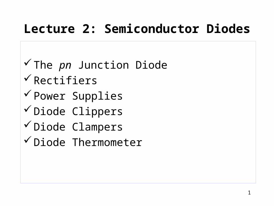
Lecture 2: Semiconductor Diodes
The pn Junction DiodeRectifiersPower SuppliesDiode ClippersDiode ClampersDiode Thermometer

2
Diodes
• Diodes are semiconductor devices which might be described as passing current in one direction only. Diodes however are far more versatile devices than that.
• Diodes may be used as voltage regulators, tuning devices in RF tuned circuits, frequency multiplying devices in RF circuits, mixing devices in RF circuits, switching applications or can be used to make logic decisions in digital circuits.
• There are also diodes which emit “light”, of course these are known as light-emitting-diodes or LED’s.
3
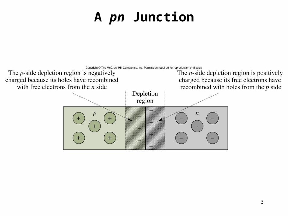
Figure 9.5
A pn Junction
4
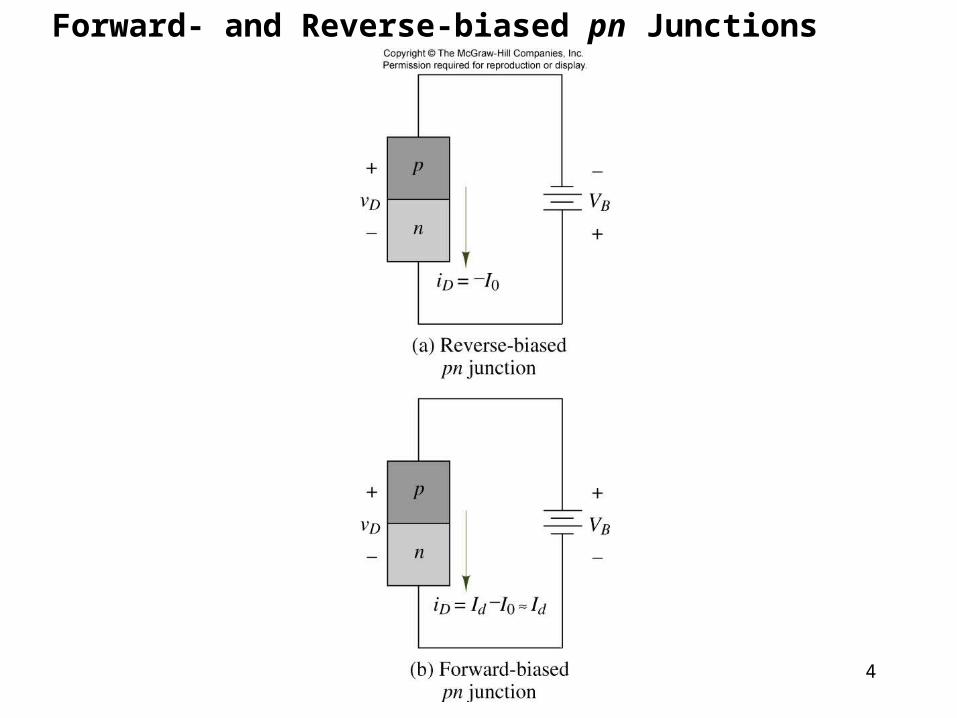
Figure 9.7
Forward- and Reverse-biased pn Junctions
5
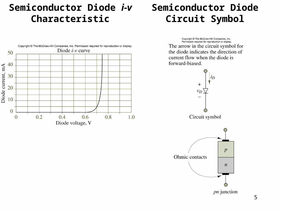
Figure 9.8, 9.9
Semiconductor Diode i-v Characteristic
Semiconductor Diode Circuit Symbol
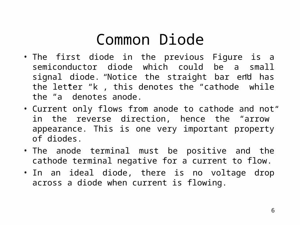
6
Common Diode• The first diode in the previous Figure is a semiconductor
diode which could be a small signal diode. Notice the straight bar end has the letter “k”, this denotes the “cathode” while the “a” denotes anode.
• Current only flows from anode to cathode and not in the reverse direction, hence the “arrow” appearance. This is one very important property of diodes.
• The anode terminal must be positive and the cathode terminal negative for a current to flow.
• In an ideal diode, there is no voltage drop across a diode when current is flowing.
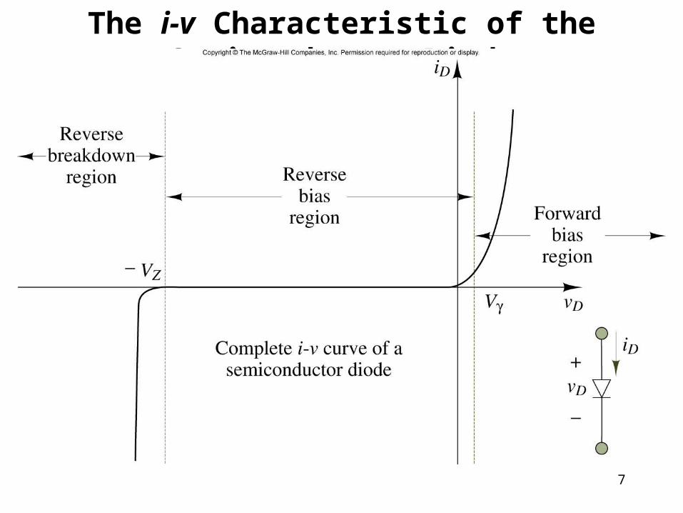
7Figure 9.10
The i-v Characteristic of the Semiconductor Diode
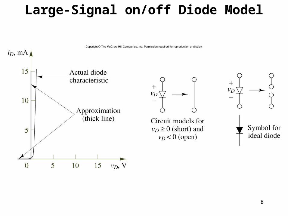
8
Figure 9.11
Large-Signal on/off Diode Model
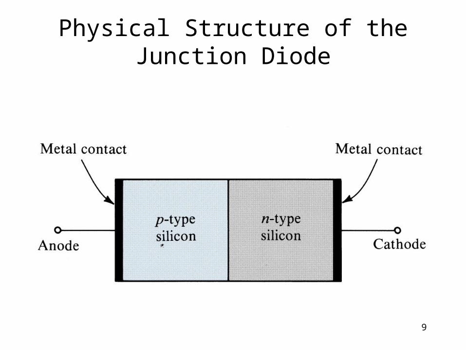
9
Physical Structure of the Junction Diode
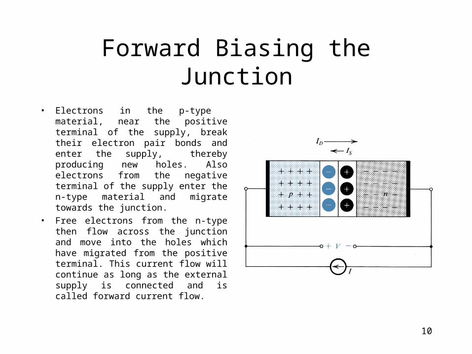
10
Forward Biasing the Junction
• Electrons in the p-type material, near the positive terminal of the supply, break their electron pair bonds and enter the supply, thereby producing new holes. Also electrons from the negative terminal of the supply enter the n-type material and migrate towards the junction.
• Free electrons from the n-type then flow across the junction and move into the holes which have migrated from the positive terminal. This current flow will continue as long as the external supply is connected and is called forward current flow.
11
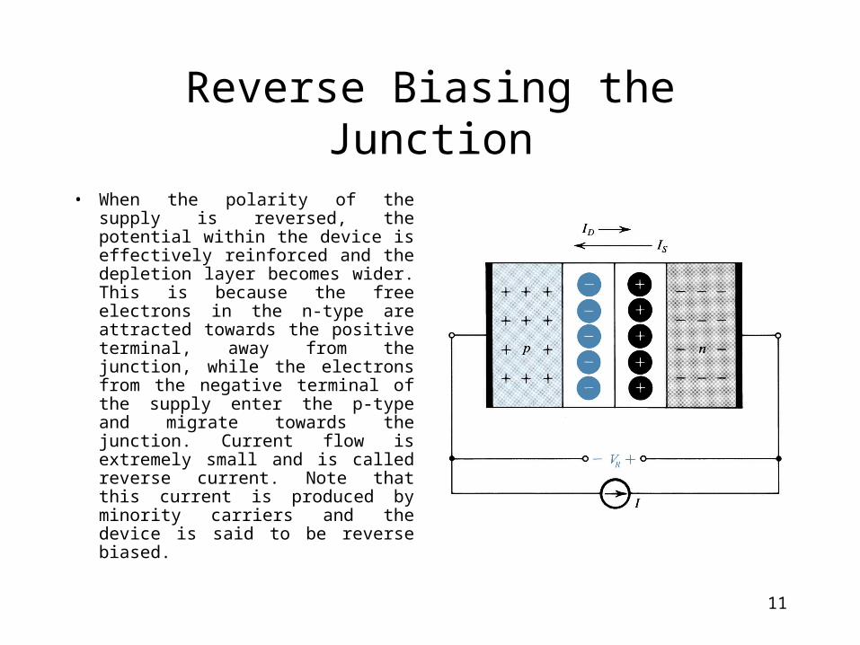
Reverse Biasing the Junction
• When the polarity of the supply is reversed, the potential within the device is effectively reinforced and the depletion layer becomes wider. This is because the free electrons in the n-type are attracted towards the positive terminal, away from the junction, while the electrons from the negative terminal of the supply enter the p-type and migrate towards the junction. Current flow is extremely small and is called reverse current. Note that this current is produced by minority carriers and the device is said to be reverse biased.
12
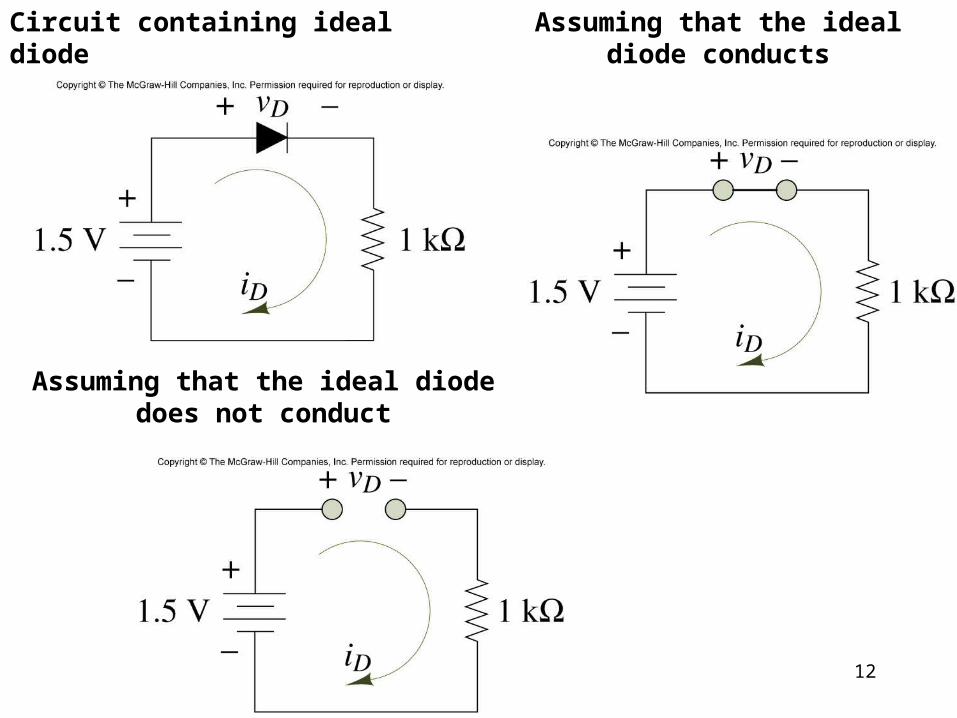
Figure 9.12, 9.13, 9.14
Circuit containing ideal diode Assuming that the ideal diode conducts
Assuming that the ideal diode does not conduct
13
Zener Diode
• The second of the diodes is a zener diode which are fairly popular for the voltage regulation of low current power supplies.
• While it is possible to obtain high current zener diodes, most regulation today is done electronically with the use of dedicated integrated circuits and pass transistors.
14
Varactor Diode
• This is actually two varactor diodes mounted back to back with the DC control voltage applied at the common junction of the cathodes. These cathodes have the double bar appearance of capacitors to indicate a varactor diode.
• When a DC control voltage is applied to the common junction of the cathodes, the capacitance exhibited by the diodes (all diodes and transistors exhibit some degree of capacitance) varies in accordance with the applied voltage.
15
Vacuum Tube
• The next diode is the simplest form of vacuum tube or valve. It simply has the old cathode and anode.
• These terms were passed on to modern solid state devices. Vacuum tube diodes are mainly only of interest to restorers and tube enthusiasts.
16
LED
• The last diode depicted is of course a light emitting diode or LED.
• A LED actually does not emit as much light as it first appears, a single LED has a plastic lens installed over it and this concentrates the amount of light.
• Seven LED’s can be arranged in a bar fashion called a seven segment LED display and when decoded properly can display the numbers 0 - 9 as well as the letters A to F.
17
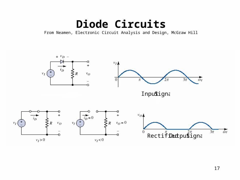
Diode CircuitsFrom Neamen, Electronic Circuit Analysis and Design, McGraw Hill
SignalInput
SignalOutput Rectified
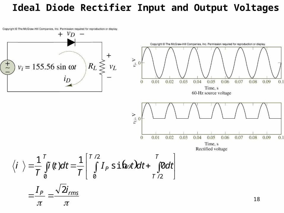
18
Figure 9.20, 9.21
Ideal Diode Rectifier Input and Output Voltages
rmsP
T T T
TP
iI
dtdttIT
dttiT
i
2
0sin1
)(1
0
2/
0 2/
19
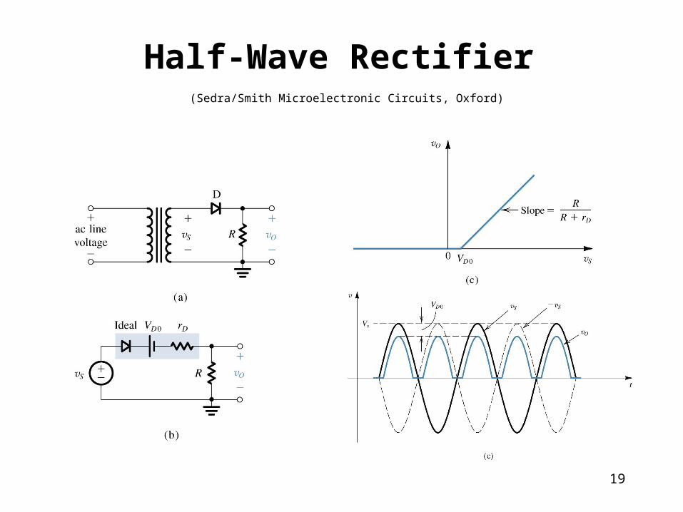
Half-Wave Rectifier (Sedra/Smith Microelectronic Circuits, Oxford)
20
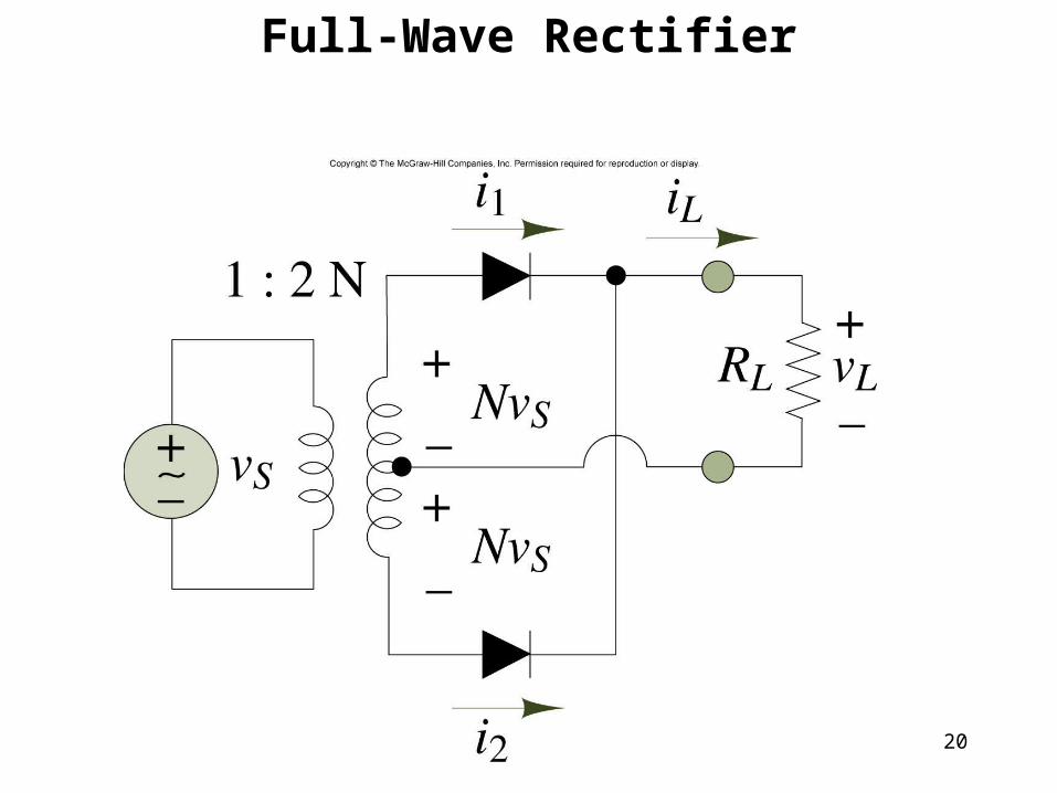
Figure 9.39
Full-Wave Rectifier
21
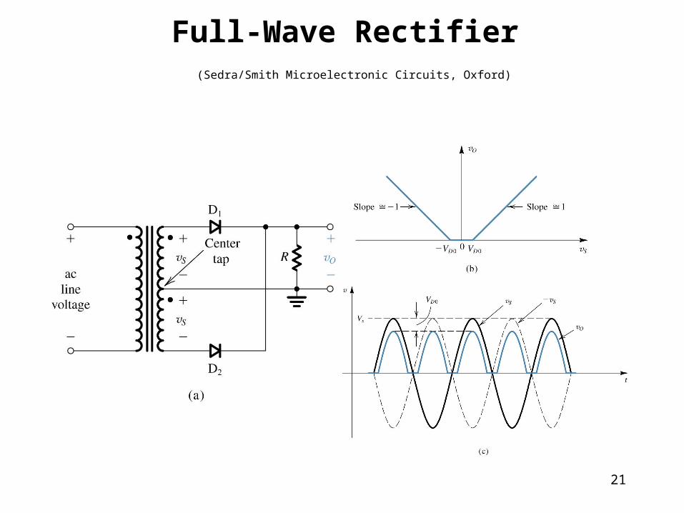
Full-Wave Rectifier (Sedra/Smith Microelectronic Circuits, Oxford)
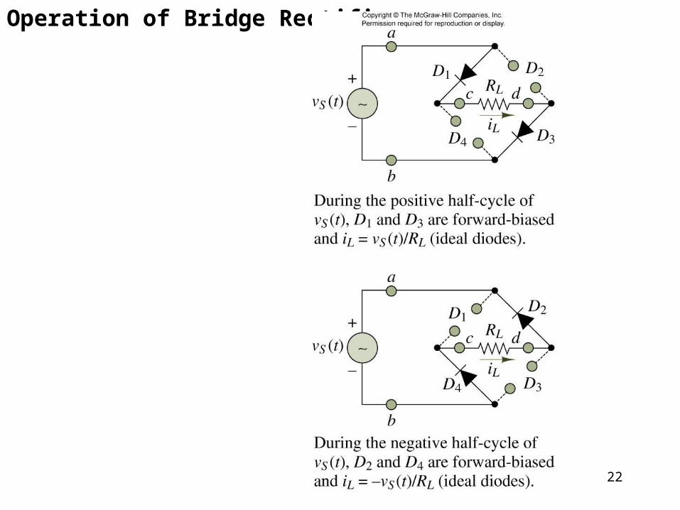
22
Figure 9.42
Operation of Bridge Rectifier
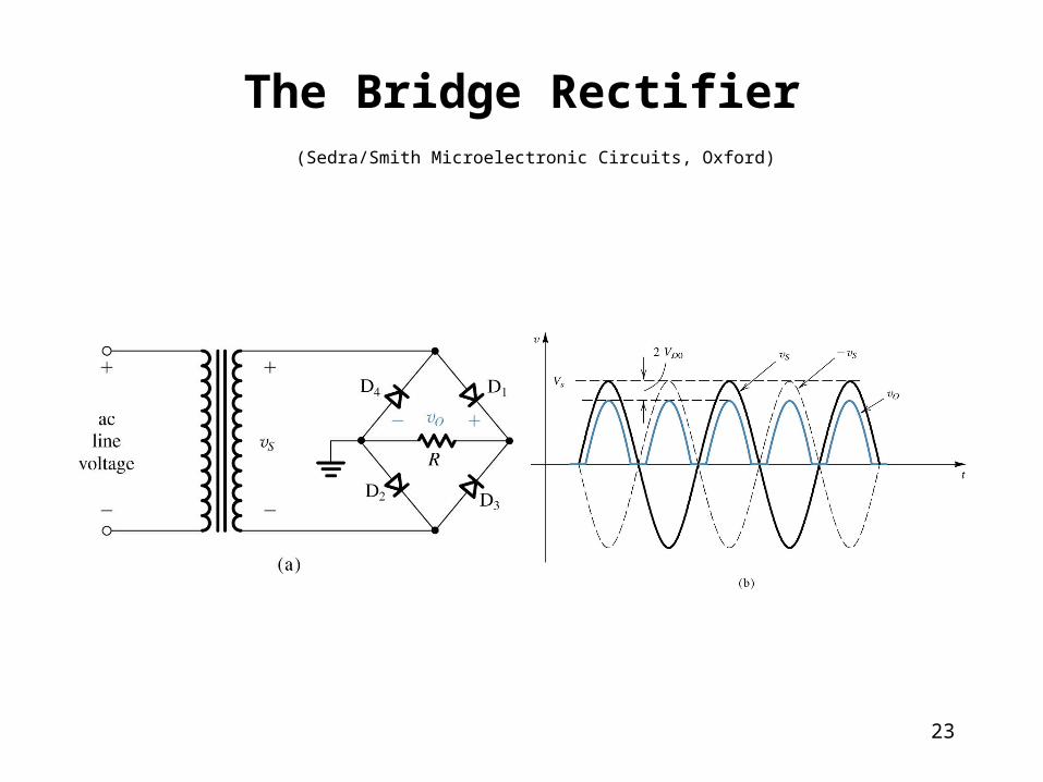
23
The Bridge Rectifier (Sedra/Smith Microelectronic Circuits, Oxford)
24
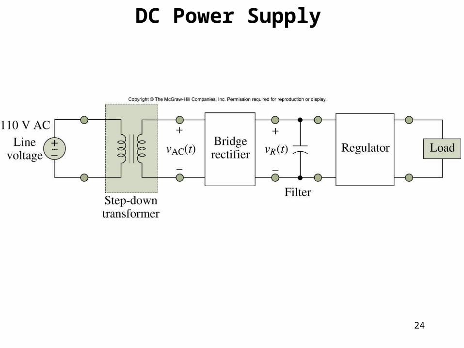
Figure 9.45
DC Power Supply
25
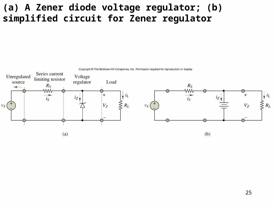
Figure 9.49
(a) A Zener diode voltage regulator; (b) simplified circuit for Zener regulator
26
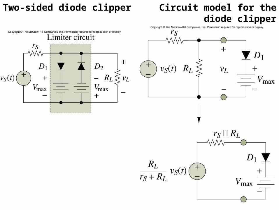
Figure 9.54, 9.55
Two-sided diode clipper Circuit model for the diode clipper
27
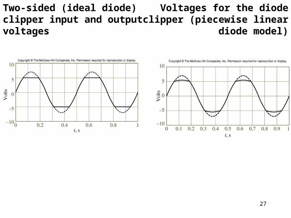
Figure 9.58, 9.60
Two-sided (ideal diode) clipper input and output voltages
Voltages for the diode clipper (piecewise linear diode model)
28
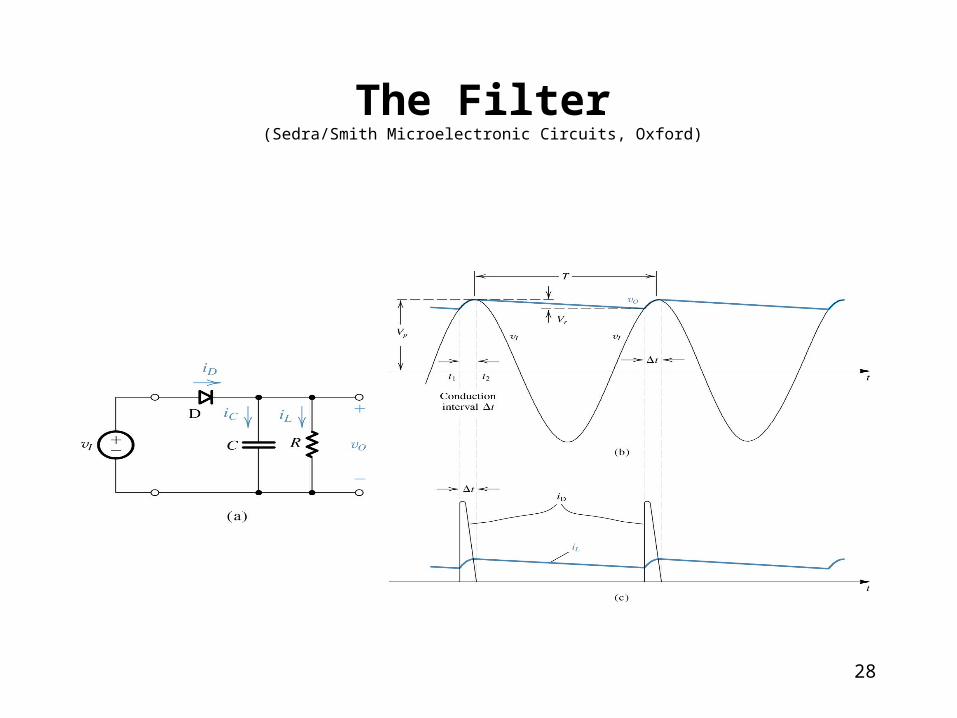
The Filter(Sedra/Smith Microelectronic Circuits, Oxford)


