256Mb: x16, x32 Mobile SDRAMFeatures
Mobile SDRAMMT48H16M16LF – 4 Meg x 16 x 4 banksMT48H8M32LF – 2 Meg x 32 x 4 banks
Features• Fully synchronous; all signals registered on positive
edge of system clock• VDD/VDDQ = 1.70–1.95V• Internal, pipelined operation; column address can
be changed every clock cycle• Four internal banks for concurrent operation• Programmable burst lengths: 1, 2, 4, 8, or
continuous page• Auto precharge, includes concurrent auto precharge• Auto refresh and self refresh modes• LVTTL-compatible inputs and outputs• On-chip temperature sensor to control refresh rate• Partial-array self refresh (PASR)• Deep power-down (DPD)• Selectable output drive (DS)• 64ms refresh period (8192 rows)
Options Marking• VDD/VDDQ
– 1.8V/1.8V H• Configuration
– 16 Meg x 16 (4 Meg x 16 x 4 banks) 16M16– 8 Meg x 32 (2 Meg x 32 x 4 banks) 8M32
• Plastic “green” package– 54-ball VFBGA (8mm x 9mm) BF– 90-ball VFBGA (8mm x 13mm) B5
• Timing – cycle time– 7.5ns at CL = 3 -75– 8ns at CL = 3 -8
• Power– Standard IDD2P/IDD7 None– Low IDD2P/IDD7 L
• Operating temperature range– Commercial (0° to +70°C) None– Industrial (–40°C to +85°C) IT
• Design revision :G
Products and specifications discussed herein are
PDF:09005aef8219eeeb/Source: 09005aef8219eedd256mb_x16_sdram_y36m_1.fm - Rev G 6/09 EN 1
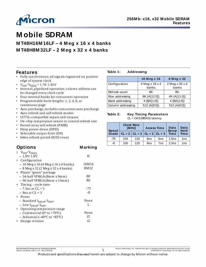
Table 1: Addressing
16 Meg x 16 8 Meg x 32
Configuration 4 Meg x 16 x 4 banks
2 Meg x 32 x 4 banks
Refresh count 8K 8K
Row addressing 8K (A[12:0]) 4K (A[11:0])
Bank addressing 4 (BA[1:0]) 4 (BA[1:0])
Column addressing 512 (A[8:0]) 512 (A[8:0])
Table 2: Key Timing ParametersCL = CAS (READ) latency
Speed Grade
Clock Rate (MHz) Access Time Data
Setup Time
Data Hold TimeCL = 2 CL = 3 CL = 2 CL = 3
-75 104 133 8ns 6ns 1.5ns 1ns-8 100 125 9ns 7ns 2.5ns 1ns
subject to change by Micron without notice.
Micron Technology, Inc., reserves the right to change products or specifications without notice.©2006 Micron Technology, Inc. All rights reserved.
PDF:09005aef8219eeeb/Source: 09005aef8219eedd Micron Technology, Inc., reserves the right to change products or specifications without notice.256mb_x16_sdram_y36m_1.fm - Rev G 6/09 EN 2 ©2006 Micron Technology, Inc. All rights reserved.
256Mb: x16, x32 Mobile SDRAMTable of Contents
Table of ContentsFeatures . . . . . . . . . . . . . . . . . . . . . . . . . . . . . . . . . . . . . . . . . . . . . . . . . . . . . . . . . . . . . . . . . . . . . . . . . . . . . . . . . . . . . . . . . . . . . .1Options . . . . . . . . . . . . . . . . . . . . . . . . . . . . . . . . . . . . . . . . . . . . . . . . . . . . . . . . . . . . . . . . . . . . . . . . . . . . . . . . . . . . . . . . . . . . . .1General Description . . . . . . . . . . . . . . . . . . . . . . . . . . . . . . . . . . . . . . . . . . . . . . . . . . . . . . . . . . . . . . . . . . . . . . . . . . . . . . . . . . .5Functional Block Diagrams. . . . . . . . . . . . . . . . . . . . . . . . . . . . . . . . . . . . . . . . . . . . . . . . . . . . . . . . . . . . . . . . . . . . . . . . . . . . .6Ball Assignments . . . . . . . . . . . . . . . . . . . . . . . . . . . . . . . . . . . . . . . . . . . . . . . . . . . . . . . . . . . . . . . . . . . . . . . . . . . . . . . . . . . . . .8Ball Descriptions . . . . . . . . . . . . . . . . . . . . . . . . . . . . . . . . . . . . . . . . . . . . . . . . . . . . . . . . . . . . . . . . . . . . . . . . . . . . . . . . . . . . .10Functional Description . . . . . . . . . . . . . . . . . . . . . . . . . . . . . . . . . . . . . . . . . . . . . . . . . . . . . . . . . . . . . . . . . . . . . . . . . . . . . . .12Initialization . . . . . . . . . . . . . . . . . . . . . . . . . . . . . . . . . . . . . . . . . . . . . . . . . . . . . . . . . . . . . . . . . . . . . . . . . . . . . . . . . . . . . . . . .12Register Definition . . . . . . . . . . . . . . . . . . . . . . . . . . . . . . . . . . . . . . . . . . . . . . . . . . . . . . . . . . . . . . . . . . . . . . . . . . . . . . . . . . .13
Mode Register . . . . . . . . . . . . . . . . . . . . . . . . . . . . . . . . . . . . . . . . . . . . . . . . . . . . . . . . . . . . . . . . . . . . . . . . . . . . . . . . . . . . .13Extended Mode Register (EMR) . . . . . . . . . . . . . . . . . . . . . . . . . . . . . . . . . . . . . . . . . . . . . . . . . . . . . . . . . . . . . . . . . . . . .16
Commands . . . . . . . . . . . . . . . . . . . . . . . . . . . . . . . . . . . . . . . . . . . . . . . . . . . . . . . . . . . . . . . . . . . . . . . . . . . . . . . . . . . . . . . . . .19Operations . . . . . . . . . . . . . . . . . . . . . . . . . . . . . . . . . . . . . . . . . . . . . . . . . . . . . . . . . . . . . . . . . . . . . . . . . . . . . . . . . . . . . . . . . .23
Bank/Row Activation. . . . . . . . . . . . . . . . . . . . . . . . . . . . . . . . . . . . . . . . . . . . . . . . . . . . . . . . . . . . . . . . . . . . . . . . . . . . . . .23READs . . . . . . . . . . . . . . . . . . . . . . . . . . . . . . . . . . . . . . . . . . . . . . . . . . . . . . . . . . . . . . . . . . . . . . . . . . . . . . . . . . . . . . . . . . . .24WRITEs . . . . . . . . . . . . . . . . . . . . . . . . . . . . . . . . . . . . . . . . . . . . . . . . . . . . . . . . . . . . . . . . . . . . . . . . . . . . . . . . . . . . . . . . . . .30
Truth Tables . . . . . . . . . . . . . . . . . . . . . . . . . . . . . . . . . . . . . . . . . . . . . . . . . . . . . . . . . . . . . . . . . . . . . . . . . . . . . . . . . . . . . . . . .40Electrical Specifications. . . . . . . . . . . . . . . . . . . . . . . . . . . . . . . . . . . . . . . . . . . . . . . . . . . . . . . . . . . . . . . . . . . . . . . . . . . . . . .45
Absolute Maximum Ratings . . . . . . . . . . . . . . . . . . . . . . . . . . . . . . . . . . . . . . . . . . . . . . . . . . . . . . . . . . . . . . . . . . . . . . . . .45Notes . . . . . . . . . . . . . . . . . . . . . . . . . . . . . . . . . . . . . . . . . . . . . . . . . . . . . . . . . . . . . . . . . . . . . . . . . . . . . . . . . . . . . . . . . . . . . . .52Timing Diagrams. . . . . . . . . . . . . . . . . . . . . . . . . . . . . . . . . . . . . . . . . . . . . . . . . . . . . . . . . . . . . . . . . . . . . . . . . . . . . . . . . . . . .54Package Dimensions . . . . . . . . . . . . . . . . . . . . . . . . . . . . . . . . . . . . . . . . . . . . . . . . . . . . . . . . . . . . . . . . . . . . . . . . . . . . . . . . .73Revision History. . . . . . . . . . . . . . . . . . . . . . . . . . . . . . . . . . . . . . . . . . . . . . . . . . . . . . . . . . . . . . . . . . . . . . . . . . . . . . . . . . . . . .75
PDF:09005aef8219eeeb/Source: 09005aef8219eedd Micron Technology, Inc., reserves the right to change products or specifications without notice.256mb_x16_sdram_y36m_1.fm - Rev G 6/09 EN 3 ©2006 Micron Technology, Inc. All rights reserved.
256Mb: x16, x32 Mobile SDRAMList of Figures
List of FiguresFigure 1: 256Mb Mobile SDRAM Part Numbering . . . . . . . . . . . . . . . . . . . . . . . . . . . . . . . . . . . . . . . . . . . . . . . . . . . . .5Figure 2: 16 Meg x 16 SDRAM . . . . . . . . . . . . . . . . . . . . . . . . . . . . . . . . . . . . . . . . . . . . . . . . . . . . . . . . . . . . . . . . . . . . . . .6Figure 3: 8 Meg x 32 SDRAM . . . . . . . . . . . . . . . . . . . . . . . . . . . . . . . . . . . . . . . . . . . . . . . . . . . . . . . . . . . . . . . . . . . . . . . .7Figure 4: 54-Ball FBGA (Top View) – 8mm x 9mm . . . . . . . . . . . . . . . . . . . . . . . . . . . . . . . . . . . . . . . . . . . . . . . . . . . . .8Figure 5: 90-Ball VFBGA (Top View) – 8mm x 13mm . . . . . . . . . . . . . . . . . . . . . . . . . . . . . . . . . . . . . . . . . . . . . . . . . . .9Figure 6: Mode Register Definition . . . . . . . . . . . . . . . . . . . . . . . . . . . . . . . . . . . . . . . . . . . . . . . . . . . . . . . . . . . . . . . . .14Figure 7: CAS Latency . . . . . . . . . . . . . . . . . . . . . . . . . . . . . . . . . . . . . . . . . . . . . . . . . . . . . . . . . . . . . . . . . . . . . . . . . . . . .16Figure 8: EMR Definition . . . . . . . . . . . . . . . . . . . . . . . . . . . . . . . . . . . . . . . . . . . . . . . . . . . . . . . . . . . . . . . . . . . . . . . . . .17Figure 9: Activating a Specific Row in a Specific Bank. . . . . . . . . . . . . . . . . . . . . . . . . . . . . . . . . . . . . . . . . . . . . . . . .23Figure 10: Example: Meeting tRCD (MIN) When 2 < tRCD (MIN)/tCK < 3 . . . . . . . . . . . . . . . . . . . . . . . . . . . . . . . .24Figure 11: READ Command. . . . . . . . . . . . . . . . . . . . . . . . . . . . . . . . . . . . . . . . . . . . . . . . . . . . . . . . . . . . . . . . . . . . . . . . .24Figure 12: Consecutive READ Bursts . . . . . . . . . . . . . . . . . . . . . . . . . . . . . . . . . . . . . . . . . . . . . . . . . . . . . . . . . . . . . . . . .25Figure 13: Random READ Accesses . . . . . . . . . . . . . . . . . . . . . . . . . . . . . . . . . . . . . . . . . . . . . . . . . . . . . . . . . . . . . . . . . .26Figure 14: READ-to-WRITE . . . . . . . . . . . . . . . . . . . . . . . . . . . . . . . . . . . . . . . . . . . . . . . . . . . . . . . . . . . . . . . . . . . . . . . . .27Figure 15: READ-to-WRITE with Extra Clock Cycle . . . . . . . . . . . . . . . . . . . . . . . . . . . . . . . . . . . . . . . . . . . . . . . . . . . .28Figure 16: READ-to-PRECHARGE . . . . . . . . . . . . . . . . . . . . . . . . . . . . . . . . . . . . . . . . . . . . . . . . . . . . . . . . . . . . . . . . . . .28Figure 17: Terminating a READ Burst . . . . . . . . . . . . . . . . . . . . . . . . . . . . . . . . . . . . . . . . . . . . . . . . . . . . . . . . . . . . . . . .29Figure 18: WRITE Command. . . . . . . . . . . . . . . . . . . . . . . . . . . . . . . . . . . . . . . . . . . . . . . . . . . . . . . . . . . . . . . . . . . . . . . .30Figure 19: WRITE Burst. . . . . . . . . . . . . . . . . . . . . . . . . . . . . . . . . . . . . . . . . . . . . . . . . . . . . . . . . . . . . . . . . . . . . . . . . . . . .31Figure 20: WRITE-to-WRITE . . . . . . . . . . . . . . . . . . . . . . . . . . . . . . . . . . . . . . . . . . . . . . . . . . . . . . . . . . . . . . . . . . . . . . . .31Figure 21: Random WRITE Cycles . . . . . . . . . . . . . . . . . . . . . . . . . . . . . . . . . . . . . . . . . . . . . . . . . . . . . . . . . . . . . . . . . . .32Figure 22: WRITE-to-READ . . . . . . . . . . . . . . . . . . . . . . . . . . . . . . . . . . . . . . . . . . . . . . . . . . . . . . . . . . . . . . . . . . . . . . . . .32Figure 23: WRITE-to-PRECHARGE . . . . . . . . . . . . . . . . . . . . . . . . . . . . . . . . . . . . . . . . . . . . . . . . . . . . . . . . . . . . . . . . . .33Figure 24: Terminating a WRITE Burst . . . . . . . . . . . . . . . . . . . . . . . . . . . . . . . . . . . . . . . . . . . . . . . . . . . . . . . . . . . . . . .33Figure 25: PRECHARGE Command . . . . . . . . . . . . . . . . . . . . . . . . . . . . . . . . . . . . . . . . . . . . . . . . . . . . . . . . . . . . . . . . . .34Figure 26: Power-Down . . . . . . . . . . . . . . . . . . . . . . . . . . . . . . . . . . . . . . . . . . . . . . . . . . . . . . . . . . . . . . . . . . . . . . . . . . . .35Figure 27: Clock Suspend During WRITE Burst . . . . . . . . . . . . . . . . . . . . . . . . . . . . . . . . . . . . . . . . . . . . . . . . . . . . . . .36Figure 28: Clock Suspend During READ Burst . . . . . . . . . . . . . . . . . . . . . . . . . . . . . . . . . . . . . . . . . . . . . . . . . . . . . . . .37Figure 29: READ with Auto Precharge Interrupted by a READ . . . . . . . . . . . . . . . . . . . . . . . . . . . . . . . . . . . . . . . . . .37Figure 30: READ with Auto Precharge Interrupted by a WRITE . . . . . . . . . . . . . . . . . . . . . . . . . . . . . . . . . . . . . . . . .38Figure 31: WRITE with Auto Precharge Interrupted by a READ . . . . . . . . . . . . . . . . . . . . . . . . . . . . . . . . . . . . . . . . .39Figure 32: WRITE with Auto Precharge Interrupted by a WRITE . . . . . . . . . . . . . . . . . . . . . . . . . . . . . . . . . . . . . . . .39Figure 33: Typical Self Refresh Current vs. Temperature . . . . . . . . . . . . . . . . . . . . . . . . . . . . . . . . . . . . . . . . . . . . . . .50Figure 34: Initialize and Load Mode Register . . . . . . . . . . . . . . . . . . . . . . . . . . . . . . . . . . . . . . . . . . . . . . . . . . . . . . . . .54Figure 35: Power-Down Mode . . . . . . . . . . . . . . . . . . . . . . . . . . . . . . . . . . . . . . . . . . . . . . . . . . . . . . . . . . . . . . . . . . . . . .55Figure 36: Clock Suspend Mode . . . . . . . . . . . . . . . . . . . . . . . . . . . . . . . . . . . . . . . . . . . . . . . . . . . . . . . . . . . . . . . . . . . . .56Figure 37: Auto Refresh Mode . . . . . . . . . . . . . . . . . . . . . . . . . . . . . . . . . . . . . . . . . . . . . . . . . . . . . . . . . . . . . . . . . . . . . . .57Figure 38: Self Refresh Mode . . . . . . . . . . . . . . . . . . . . . . . . . . . . . . . . . . . . . . . . . . . . . . . . . . . . . . . . . . . . . . . . . . . . . . . .58Figure 39: READ – without Auto Precharge . . . . . . . . . . . . . . . . . . . . . . . . . . . . . . . . . . . . . . . . . . . . . . . . . . . . . . . . . . .59Figure 40: READ – with Auto Precharge . . . . . . . . . . . . . . . . . . . . . . . . . . . . . . . . . . . . . . . . . . . . . . . . . . . . . . . . . . . . . .60Figure 41: Single READ – without Auto Precharge . . . . . . . . . . . . . . . . . . . . . . . . . . . . . . . . . . . . . . . . . . . . . . . . . . . . .61Figure 42: Single READ – with Auto Precharge . . . . . . . . . . . . . . . . . . . . . . . . . . . . . . . . . . . . . . . . . . . . . . . . . . . . . . . .62Figure 43: Alternating Bank Read Accesses . . . . . . . . . . . . . . . . . . . . . . . . . . . . . . . . . . . . . . . . . . . . . . . . . . . . . . . . . . .63Figure 44: READ – Continuous Page Burst . . . . . . . . . . . . . . . . . . . . . . . . . . . . . . . . . . . . . . . . . . . . . . . . . . . . . . . . . . . .64Figure 45: READ – DQM Operation . . . . . . . . . . . . . . . . . . . . . . . . . . . . . . . . . . . . . . . . . . . . . . . . . . . . . . . . . . . . . . . . . .65Figure 46: WRITE – Without Auto Precharge . . . . . . . . . . . . . . . . . . . . . . . . . . . . . . . . . . . . . . . . . . . . . . . . . . . . . . . . . .66Figure 47: WRITE – with Auto Precharge . . . . . . . . . . . . . . . . . . . . . . . . . . . . . . . . . . . . . . . . . . . . . . . . . . . . . . . . . . . . .67Figure 48: Single WRITE – Without Auto Precharge . . . . . . . . . . . . . . . . . . . . . . . . . . . . . . . . . . . . . . . . . . . . . . . . . . . .68Figure 49: Single WRITE – with Auto Precharge . . . . . . . . . . . . . . . . . . . . . . . . . . . . . . . . . . . . . . . . . . . . . . . . . . . . . . .69Figure 50: Alternating Bank Write Accesses . . . . . . . . . . . . . . . . . . . . . . . . . . . . . . . . . . . . . . . . . . . . . . . . . . . . . . . . . . .70Figure 51: WRITE – Continuous Page Burst . . . . . . . . . . . . . . . . . . . . . . . . . . . . . . . . . . . . . . . . . . . . . . . . . . . . . . . . . . .71Figure 52: WRITE – DQM Operation . . . . . . . . . . . . . . . . . . . . . . . . . . . . . . . . . . . . . . . . . . . . . . . . . . . . . . . . . . . . . . . . .72Figure 53: 54-Ball VFBGA (8mm x 9mm) . . . . . . . . . . . . . . . . . . . . . . . . . . . . . . . . . . . . . . . . . . . . . . . . . . . . . . . . . . . . .73Figure 54: 90-Ball VFBGA (8mm x 13mm) . . . . . . . . . . . . . . . . . . . . . . . . . . . . . . . . . . . . . . . . . . . . . . . . . . . . . . . . . . . .74

PDF:09005aef8219eeeb/Source: 09005aef8219eedd Micron Technology, Inc., reserves the right to change products or specifications without notice.256mb_x16_sdram_y36m_1.fm - Rev G 6/09 EN 4 ©2006 Micron Technology, Inc. All rights reserved.
256Mb: x16, x32 Mobile SDRAMList of Tables
List of TablesTable 1: Addressing . . . . . . . . . . . . . . . . . . . . . . . . . . . . . . . . . . . . . . . . . . . . . . . . . . . . . . . . . . . . . . . . . . . . . . . . . . . . . . .1Table 2: Key Timing Parameters . . . . . . . . . . . . . . . . . . . . . . . . . . . . . . . . . . . . . . . . . . . . . . . . . . . . . . . . . . . . . . . . . . . .1Table 3: VFBGA Ball Descriptions. . . . . . . . . . . . . . . . . . . . . . . . . . . . . . . . . . . . . . . . . . . . . . . . . . . . . . . . . . . . . . . . . .10Table 4: Burst Definition Table . . . . . . . . . . . . . . . . . . . . . . . . . . . . . . . . . . . . . . . . . . . . . . . . . . . . . . . . . . . . . . . . . . . .15Table 5: Truth Table – Commands and DQM Operation . . . . . . . . . . . . . . . . . . . . . . . . . . . . . . . . . . . . . . . . . . . . .19Table 6: Truth Table – CKE. . . . . . . . . . . . . . . . . . . . . . . . . . . . . . . . . . . . . . . . . . . . . . . . . . . . . . . . . . . . . . . . . . . . . . . .40Table 7: Truth Table – Current State Bank n, Command to Bank n . . . . . . . . . . . . . . . . . . . . . . . . . . . . . . . . . . . .41Table 8: Truth Table – Current State Bank n, Command to Bank m. . . . . . . . . . . . . . . . . . . . . . . . . . . . . . . . . . . .43Table 9: Absolute Maximum Ratings . . . . . . . . . . . . . . . . . . . . . . . . . . . . . . . . . . . . . . . . . . . . . . . . . . . . . . . . . . . . . . .45Table 10: DC Electrical Characteristics and Operating Conditions. . . . . . . . . . . . . . . . . . . . . . . . . . . . . . . . . . . . . .45Table 11: Electrical Characteristics and Recommended AC Operating Conditions . . . . . . . . . . . . . . . . . . . . . . .46Table 12: AC Functional Characteristics . . . . . . . . . . . . . . . . . . . . . . . . . . . . . . . . . . . . . . . . . . . . . . . . . . . . . . . . . . . . .47Table 13: IDD Specifications and Conditions (x16) . . . . . . . . . . . . . . . . . . . . . . . . . . . . . . . . . . . . . . . . . . . . . . . . . . . .48Table 14: IDD Specifications and Conditions (x32) . . . . . . . . . . . . . . . . . . . . . . . . . . . . . . . . . . . . . . . . . . . . . . . . . . . .49Table 15: IDD7 – Self Refresh Current Options . . . . . . . . . . . . . . . . . . . . . . . . . . . . . . . . . . . . . . . . . . . . . . . . . . . . . . . .50Table 16: Capacitance . . . . . . . . . . . . . . . . . . . . . . . . . . . . . . . . . . . . . . . . . . . . . . . . . . . . . . . . . . . . . . . . . . . . . . . . . . . . .51

256Mb: x16, x32 Mobile SDRAMGeneral Description
Figure 1: 256Mb Mobile SDRAM Part Numbering
General DescriptionThe Micron® 256Mb Mobile SDRAM is a high-speed CMOS, dynamic random-access memory containing 268,435,456-bits. It is internally configured as a quad-bank DRAM with a synchronous interface (all signals are registered on the positive edge of the clock signal, CLK). Each of the x16’s 67,108,864-bit banks is organized as 8192 rows by 512 col-umns by 16 bits. Each of the x32’s 67,108,864-bit banks is organized as 4096 rows by 512 columns by 32 bits.
Read and write accesses to the SDRAM are burst oriented; accesses start at a selected location and continue for a programmed number of locations in a programmed sequence. Accesses begin with the registration of an ACTIVE command, which is then followed by a READ or WRITE command. The address bits registered coincident with the ACTIVE command are used to select the bank and row to be accessed. The address bits registered coincident with the READ or WRITE command are used to select the starting column location for the burst access.
The SDRAM provides for programmable read or write burst lengths (BLs) of 1, 2, 4, or 8 locations, or continuous page burst, with a read burst terminate option. An auto pre-charge function may be enabled to provide a self-timed row precharge that is initiated at the end of the burst sequence.
The 256Mb SDRAM uses an internal pipelined architecture to achieve high-speed opera-tion. It also allows the column address to be changed on every clock cycle to achieve a high-speed, fully random access. Precharging one bank while accessing one of the other three banks will hide the precharge cycles and provide seamless high-speed, random-access operation.
Speed Grade tCK = 7.5ns
tCK = 8.0ns
-75
-8
IT
Operating Temp.
Commercial
Industrial
L
Power
Standard IDD2P/IDD7
Low IDD2P/IDD7
Example Part Number: MT48H8M32LFB5-75LIT
MobileConfigurationMT48 Package Speed Temp.
Power
Configuration
16 Meg x 16
8 Meg x 32
16M16LF
8M32LF
Package
8 x 9 VFBGA (lead-free)
8 x 13 VFBGA (lead-free)
H
VDD/VDDQ
VDD/VDDQ
1.8V/1.8V
BF
B5
Revision–
Revision
:G Design Revision
PDF:09005aef8219eeeb/Source: 09005aef8219eedd Micron Technology, Inc., reserves the right to change products or specifications without notice.256mb_x16_sdram_y36m_1.fm - Rev G 6/09 EN 5 ©2006 Micron Technology, Inc. All rights reserved.

256Mb: x16, x32 Mobile SDRAMFunctional Block Diagrams
The 256Mb SDRAM is designed to operate in 1.8V low-power memory systems. An auto refresh mode is provided, along with a power-saving deep power-down mode. All inputs and outputs are LVTTL-compatible.
SDRAM offers substantial advances in DRAM operating performance, including the abil-ity to synchronously burst data at a high data rate with automatic column-address gen-eration, the ability to interleave between internal banks in order to hide precharge time, and the capability to randomly change column addresses on each clock cycle during a burst access.
Functional Block Diagrams
Figure 2: 16 Meg x 16 SDRAM
13
RAS#
CAS#
ROW- ADDRESS
MUX
CLK
CS#
WE#
CKE
CONTROL LOGIC
COLUMN- ADDRESS COUNTER/
LATCH
MODE REGISTER
9
CO
MM
AN
D
DEC
OD
E
A[12:0],BA[1:0]
UDQM, LDQM 13
ADDRESS REGISTER
15
256 (x16)
8192
I/O GATING DQM MASK LOGIC READ DATA LATCH
WRITE DRIVERS
COLUMN DECODER
BANK0MEMORY
ARRAY(8192 x 512 x 16)
BANK0 ROW-
ADDRESS LATCH
& DECODER
8192
Sense amplifiers
BANK CONTROL
LOGIC
DQ[15:0]
16
16
15
Bank1 Bank2
Bank3
13
9
2
2 2
2
REFRESH COUNTER
EXT MODE REGISTER
16
BA1 BA0 Bank 0 0 0 0 1 1 1 0 2 1 1 3
DATA OUTPUT REGISTER
DATA INPUT
REGISTER
PDF:09005aef8219eeeb/Source: 09005aef8219eedd Micron Technology, Inc., reserves the right to change products or specifications without notice.256mb_x16_sdram_y36m_1.fm - Rev G 6/09 EN 6 ©2006 Micron Technology, Inc. All rights reserved.
256Mb: x16, x32 Mobile SDRAMFunctional Block Diagrams
Figure 3: 8 Meg x 32 SDRAM
13
RAS#
CAS#
ROW- ADDRESS
MUX
CLK
CS#
WE#
CKE
CONTROL LOGIC
COLUMN- ADDRESS COUNTER/
LATCH
MODE REGISTER
9
CO
MM
AN
D
DEC
OD
E
A[11:0],BA[1:0]
DQM[3:0]12
ADDRESS REGISTER
14
512 (x32)
4096
COLUMN DECODER
BANK0MEMORY
ARRAY(4096 x 512 x 32)
BANK0 ROW-
ADDRESS LATCH
& DECODER
4096
SENSE AMPLIFIERS
BANK CONTROL
LOGIC
DQ[31:0]
32
32 DATA INPUT
REGISTER
DATA OUTPUT REGISTER
32
14
BANK1 BANK2
BANK3
12
9
2
4 4
2
REFRESH COUNTER
BA1 BA0 Bank 0 0 0 0 1 1 1 0 2 1 1 3
EXT MODE REGISTER
I/O GATING DQM MASK LOGIC READ DATA LATCH
WRITE DRIVERS
PDF:09005aef8219eeeb/Source: 09005aef8219eedd Micron Technology, Inc., reserves the right to change products or specifications without notice.256mb_x16_sdram_y36m_1.fm - Rev G 6/09 EN 7 ©2006 Micron Technology, Inc. All rights reserved.

256Mb: x16, x32 Mobile SDRAMBall Assignments
Ball Assignments
Figure 4: 54-Ball FBGA (Top View) – 8mm x 9mm
VSS
DQ14
DQ12
DQ10
DQ8
UDQM
A12
A8
VSS
DQ15
DQ13
DQ11
DQ9
DNU
CLK
A11
A7
A5
VSSQ
VDDQ
VSSQ
VDDQ
VSS
CKE
A9
A6
A4
VDDQ
VSSQ
VDDQ
VSSQ
VDD
CAS#
BA0
A0
A3
DQ0
DQ2
DQ4
DQ6
LDQM
RAS#
BA1
A1
A2
VDD
DQ1
DQ3
DQ5
DQ7
WE#
CS#
A10
VDD
1 2 3 4 5 6 7 8 9
A
B
C
D
E
F
G
H
J
PDF:09005aef8219eeeb/Source: 09005aef8219eedd Micron Technology, Inc., reserves the right to change products or specifications without notice.256mb_x16_sdram_y36m_1.fm - Rev G 6/09 EN 8 ©2006 Micron Technology, Inc. All rights reserved.

256Mb: x16, x32 Mobile SDRAMBall Assignments
Figure 5: 90-Ball VFBGA (Top View) – 8mm x 13mm
DQ26
DQ28
VSSQ
VSSQ
VDDQ
VSS
A4
A7
CLK
DQM1
VDDQ
VSSQ
VSSQ
DQ11
DQ13
A
B
C
D
E
F
G
H
J
K
L
M
N
P
R
DQ24
VDDQ
DQ27
DQ29
DQ31
DQM3
A5
A8
CKE
DNU
DQ8
DQ10
DQ12
VDDQ
DQ15
VSS
VSSQ
DQ25
DQ30
NC
A3
A6
NC
A9
NC
VSS
DQ9
DQ14
VSSQ
VSS
VDD
VDDQ
DQ22
DQ17
NC
A2
A10
NC
BA0
CAS#
VDD
DQ6
DQ1
VDDQ
VDD
DQ23
VSSQ
DQ20
DQ18
DQ16
DQM2
A0
BA1
CS#
WE#
DQ7
DQ5
DQ3
VSSQ
DQ0
DQ21
DQ19
VDDQ
VDDQ
VSSQ
VDD
A1
A11
RAS#
DQM0
VSSQ
VDDQ
VDDQ
DQ4
DQ2
1 2 3 4 5 6 7 8 9
PDF:09005aef8219eeeb/Source: 09005aef8219eedd Micron Technology, Inc., reserves the right to change products or specifications without notice.256mb_x16_sdram_y36m_1.fm - Rev G 6/09 EN 9 ©2006 Micron Technology, Inc. All rights reserved.

256Mb: x16, x32 Mobile SDRAMBall Descriptions
Ball Descriptions
Table 3: VFBGA Ball Descriptions
54-Ball VFBGA 90-Ball VFBGA Symbol Type Description
F2 J1 CLK Input Clock: CLK is driven by the system clock. All SDRAM input signals are sampled on the positive edge of CLK. CLK also increments the internal burst counter and controls the output registers.
F3 J2 CKE Input Clock enable: CKE activates (HIGH) and deactivates (LOW) the CLK signal. Deactivating the clock provides precharge power-down and SELF REFRESH operation (all banks idle), ACTIVE power-down (row active in any bank), Deep power-down (all banks idle), or CLOCK SUSPEND operation (burst/access in progress). CKE is synchronous except after the device enters power-down and self refresh modes, where CKE becomes asynchronous until after exiting the same mode. The input buffers, including CLK, are disabled during power-down and self refresh modes, providing low standby power.
G9 J8 CS# Input Chip select: CS# enables (registered LOW) and disables (registered HIGH) the command decoder. All commands are masked when CS# is registered HIGH. CS# provides for external bank selection on systems with multiple banks. CS# is considered part of the command code.
F7, F8, F9 K7, J9, K8 CAS#, RAS#, WE#
Input Command inputs: RAS#, CAS#, and WE# (along with CS#) define the command being entered.
F1, E8 K9, K1, F8, F2 UDQMLDQM,
DQM[33:0]
Input Input/output mask: DQM is sampled HIGH and is an input mask signal for write accesses and an output enable signal for read accesses. Input data is masked during a WRITE cycle. The output buffers are placed in a High-Z state (two-clock latency) during a READ cycle. For the x16, LDQM corresponds to DQ[7:0] and UDQM corresponds to DQ[16:8]. For the x32, DQM0 corresponds to DQ[7:0], DQM1 corresponds to DQ[15:8], DQM2 corresponds to DQ[23:16], and DQM3 corresponds to DQ[31:24]. DQM[3:0] (or LDQM and UDQM if x16) are considered same state when referenced as DQM. DQM loading is designed to match that of DQ balls.
G7, G8 J7, H8 BA[1:0] Input Bank address input(s): BA[1:0] define to which bank the ACTIVE, READ, WRITE, or PRECHARGE command is being applied. These balls also provide the op-code during a LOAD MODE REGISTER (LMR) command. BA[1:0] become “Don’t Care” when registering an ALL BANK PRECHARGE (A10 HIGH).
H7, H8, J8, J7, J3, J2, H3, H2,
H1, G3, H9, G2, G1
G8, G9, F7, F3, G1, G2, G3, H1, H2, J3, G7, H9
A[12:0] Input Address inputs: A[12:0] are sampled during the ACTIVE command (row-address A[12:0] and READ/WRITE command (column-address A[8:0] (x32); column-address A[8:0] (x16); with A10 defining auto precharge) to select one location out of the memory array in the respective bank. A10 is sampled during a PRECHARGE command to determine if all banks are to be precharged (A10 HIGH) or bank selected by BA[1:0]. The address inputs also provide the op-code during a LMR command.
PDF:09005aef8219eeeb/Source: 09005aef8219eedd Micron Technology, Inc., reserves the right to change products or specifications without notice.256mb_x16_sdram_y36m_1.fm - Rev G 6/09 EN 10 ©2006 Micron Technology, Inc. All rights reserved.
256Mb: x16, x32 Mobile SDRAMBall Descriptions
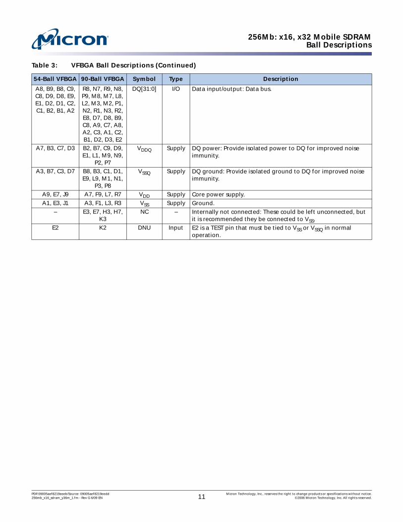
A8, B9, B8, C9, C8, D9, D8, E9, E1, D2, D1, C2, C1, B2, B1, A2
R8, N7, R9, N8, P9, M8, M7, L8, L2, M3, M2, P1, N2, R1, N3, R2, E8, D7, D8, B9, C8, A9, C7, A8, A2, C3, A1, C2, B1, D2, D3, E2
DQ[31:0] I/O Data input/output: Data bus.
A7, B3, C7, D3 B2, B7, C9, D9, E1, L1, M9, N9,
P2, P7
VDDQ Supply DQ power: Provide isolated power to DQ for improved noise immunity.
A3, B7, C3, D7 B8, B3, C1, D1, E9, L9, M1, N1,
P3, P8
VSSQ Supply DQ ground: Provide isolated ground to DQ for improved noise immunity.
A9, E7, J9 A7, F9, L7, R7 VDD Supply Core power supply.A1, E3, J1 A3, F1, L3, R3 VSS Supply Ground.
– E3, E7, H3, H7, K3
NC – Internally not connected: These could be left unconnected, but it is recommended they be connected to VSS.
E2 K2 DNU Input E2 is a TEST pin that must be tied to VSS or VSSQ in normal operation.
Table 3: VFBGA Ball Descriptions (Continued)
54-Ball VFBGA 90-Ball VFBGA Symbol Type Description
PDF:09005aef8219eeeb/Source: 09005aef8219eedd Micron Technology, Inc., reserves the right to change products or specifications without notice.256mb_x16_sdram_y36m_1.fm - Rev G 6/09 EN 11 ©2006 Micron Technology, Inc. All rights reserved.
256Mb: x16, x32 Mobile SDRAMFunctional Description
Functional DescriptionIn general, a 256Mb SDRAM is quad-bank DRAM that operates at 1.8V and includes a synchronous interface (all signals are registered on the positive edge of the clock signal, CLK).
Read and write accesses to the SDRAM are burst oriented; accesses start at a selected location and continue for a programmed number of locations in a programmed sequence. Accesses begin with the registration of an ACTIVE command, which is then followed by a READ or WRITE command. The address bits registered coincident with the ACTIVE command are used to select the bank and row to be accessed (BA[1:0] select the bank, A[12:0] select the row for x16, and A[11:0] select the row for x32). The address bits (A[8:0] for x16 and A[8:0] for x32) registered coincident with the READ or WRITE com-mand are used to select the starting column location for the burst access.
Prior to normal operation, the SDRAM must be initialized. The following sections pro-vide detailed information covering device initialization, register definition, command descriptions, and device operation.
InitializationSDRAM must be powered up and initialized in a predefined manner. Operational proce-dures other than those specified may result in undefined operation. The initialization for mobile SDRAM is as follows.1. Simultaneously apply power to VDD and VDDQ.2. After power supplies have settled, apply a stable clock signal. Stable clock is defined as
a signal cycling within timing constraints specified for the clock pin.3. Wait at least 100µs. During this period NOP or COMMAND INHIBIT commands
should be applied. No other command other than NOP or COMMAND INHIBIT isallowed during this period.
4. Preform a PRECHARGE ALL command to place the SDRAM into an all banks idlestate.
5. Wait at least tRP time. During this time NOP or COMMAND INHIBIT commands mustbe applied.
6. Issue an AUTO REFRESH command.7. Wait at least tRFC time, during which only NOP or COMMAND INHIBIT commands
are allowed.8. Issue an Auto Refresh command.9. Wait at least tRFC time, during which only NOP or COMMAND INHIBIT commands
are allowed.10. Issue a LOAD MODE REGISTER command with BA1=0, and BA0=0, to program the
mode register with desired values.11. Wait tMRD time. Only NOP or COMMAND INHIBIT commands may be applied dur-
ing this time.12. Issue a LOAD MODE REGISTER command with BA1 = 1, and BA0 = 0, to program the
extended mode register with desired values.13. Wait tMRD time. Only NOP or COMMAND INHIBIT commands may be applied dur-
ing this time.
The Mobile SDRAM is now initialized and can accept any valid command.
PDF:09005aef8219eeeb/Source: 09005aef8219eedd Micron Technology, Inc., reserves the right to change products or specifications without notice.256mb_x16_sdram_y36m_1.fm - Rev G 6/09 EN 12 ©2006 Micron Technology, Inc. All rights reserved.

256Mb: x16, x32 Mobile SDRAMRegister Definition
Register Definition
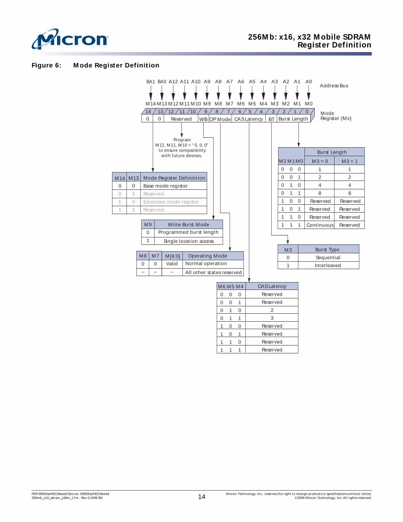
Mode Register
There are two mode registers in the component: mode register and extended mode reg-ister (EMR). The mode register is illustrated in Figure 6 on page 14. The mode register is used to define the specific mode of operation of the SDRAM. This definition includes the selection of a burst length (BL), a burst type, a CAS latency (CL), an operating mode and a write burst mode, as shown in Figure 6 on page 14. The mode register is programmed via the LMR command and will retain the stored information until it is programmed again or the device loses power.
Mode register bits M[2:0] specify the BL, M3 specifies the type of burst, M[6:4] specify the CL, M[8:7] specify the operating mode, M9 specifies the write burst mode, and M[11:10] should be set to zero.
The mode register must be loaded when all banks are idle, and the controller must wait tMRD before initiating the subsequent operation. Violating either of these requirements will result in unspecified operation.
Burst Length (BL)
Read and write accesses to the SDRAM are burst oriented, with the BL being program-mable, as shown in Figure 6 on page 14. The BL determines the maximum number of column locations that can be accessed for a given READ or WRITE command. BL = 1, 2, 4, 8 locations are available for both the sequential and the interleaved burst types, and a continuous page burst is available for the sequential type. The continuous page burst is used in conjunction with the BURST TERMINATE command to generate arbitrary burst lengths.
Reserved states should not be used, as unknown operation or incompatibility with future versions may result.
When a READ or WRITE command is issued, a block of columns equal to the BL is effec-tively selected. All accesses for that burst take place within this block, meaning that the burst will wrap within the block if a boundary is reached. The block is uniquely selected by A[8:1] when BL = 2, A[8:2] when BL = 4, and A[8:3] when BL = 8. The remaining (least significant) address bit(s) is (are) used to select the starting location within the block. Continuous page bursts wrap within the page if the boundary is reached.
Burst Type
Accesses within a given burst may be programmed to be either sequential or interleaved; this is referred to as the burst type and is selected via bit M3.
The ordering of accesses within a burst is determined by the BL, the burst type, and the starting column address, as shown in Table 4 on page 15.
PDF:09005aef8219eeeb/Source: 09005aef8219eedd Micron Technology, Inc., reserves the right to change products or specifications without notice.256mb_x16_sdram_y36m_1.fm - Rev G 6/09 EN 13 ©2006 Micron Technology, Inc. All rights reserved.
256Mb: x16, x32 Mobile SDRAMRegister Definition
Figure 6: Mode Register Definition
M3 = 0
1
2
4
8
Reserved
Reserved
Reserved
Continuous
M3 = 1
1
2
4
8
Reserved
Reserved
Reserved
Reserved
0
1
Burst Type
Sequential
Interleaved
CAS Latency
Reserved
Reserved
2
3
Reserved
Reserved
Reserved
Reserved
Burst Length
M0
0
1
0
1
0
1
0
1
M1
0
0
1
1
0
0
1
1
M2
0
0
0
0
1
1
1
1
M3
M4
0
1
0
1
0
1
0
1
M5
0
0
1
1
0
0
1
1
M6
0
0
0
0
1
1
1
1
0
0
1
1
0
1
0
1
Mode Register (Mx)
Address Bus
M8
0
–
M7
0
–
Operating Mode
Valid
–
Normal operation
All other states reserved
Mode Register Definintion
Base mode register
Reserved
Extended mode register
Reserved
M14 M13
M9
0
1
Write Burst Mode
Programmed burst length
Single location access
ProgramM12, M11, M10 = “0, 0, 0”
to ensure compatibilitywith future devices.
9 7 6 5 4 3 8 2 1 Burst Length0
M12
A11
M11
A10
M10
A9
M9
A8
M8
A7
M7
A6
M6
A5
M5
A4
M4
A3
M3
A2
M2
A1
M1
A0
M0
10 11 12
BA0 A12
M13
BA1
M14
013 14 0
BTCAS LatencyOP ModeWBReserved
M[6:0]
PDF:09005aef8219eeeb/Source: 09005aef8219eedd Micron Technology, Inc., reserves the right to change products or specifications without notice.256mb_x16_sdram_y36m_1.fm - Rev G 6/09 EN 14 ©2006 Micron Technology, Inc. All rights reserved.

256Mb: x16, x32 Mobile SDRAMRegister Definition
CAS Latency (CL)
The CL is the delay, in clock cycles, between the registration of a READ command and the availability of the first piece of output data. The latency can be set to two or three clocks.
If a READ command is registered at clock edge n, and the latency is m clocks, the data will be available by clock edge n + m. The DQs will start driving as a result of the clock edge one cycle earlier (n + m - 1), and provided that the relevant access times are met, the data will be valid by clock edge n + m. For example, assuming that the clock cycle time is such that all relevant access times are met, if a READ command is registered at T0 and the latency is programmed to two clocks, the DQs will start driving after T1 and the data will be valid by T2, as shown in Figure 7 on page 16.
Reserved states should not be used as unknown operation or incompatibility with future versions may result.
Table 4: Burst Definition Table
Burst Length Starting Column Address
Order of Accesses Within a Burst
Type = Sequential Type = Interleaved
2 A00 0-1 0-11 1-0 1-0
4 A1 A00 0 0-1-2-3 0-1-2-30 1 1-2-3-0 1-0-3-21 0 2-3-0-1 2-3-0-11 1 3-0-1-2 3-2-1-0
8 A2 A1 A00 0 0 0-1-2-3-4-5-6-7 0-1-2-3-4-5-6-70 0 1 1-2-3-4-5-6-7-0 1-0-3-2-5-4-7-60 1 0 2-3-4-5-6-7-0-1 2-3-0-1-6-7-4-50 1 1 3-4-5-6-7-0-1-2 3-2-1-0-7-6-5-41 0 0 4-5-6-7-0-1-2-3 4-5-6-7-0-1-2-31 0 1 5-6-7-0-1-2-3-4 5-4-7-6-1-0-3-21 1 0 6-7-0-1-2-3-4-5 6-7-4-5-2-3-0-11 1 1 7-0-1-2-3-4-5-6 7-6-5-4-3-2-1-0
Continuous Page
n = A[8:0] Cn, Cn + 1, Cn + 2Cn + 3,
Cn + 4…,…Cn - 1,
Cn…
Not supported
PDF:09005aef8219eeeb/Source: 09005aef8219eedd Micron Technology, Inc., reserves the right to change products or specifications without notice.256mb_x16_sdram_y36m_1.fm - Rev G 6/09 EN 15 ©2006 Micron Technology, Inc. All rights reserved.

256Mb: x16, x32 Mobile SDRAMRegister Definition
Figure 7: CAS Latency
Operating Mode
The normal operating mode is selected by setting M7 and M8 to zero; the other combi-nations of values for M7 and M8 are reserved for future use.
Reserved states should not be used as unknown operation or incompatibility with future versions may result.
Write Burst Mode
When M9 = 0, the BL programmed via M[2:0] applies to both READ and WRITE bursts; when M9 = 1, the programmed BL applies to READ bursts, but write accesses are single-location accesses.
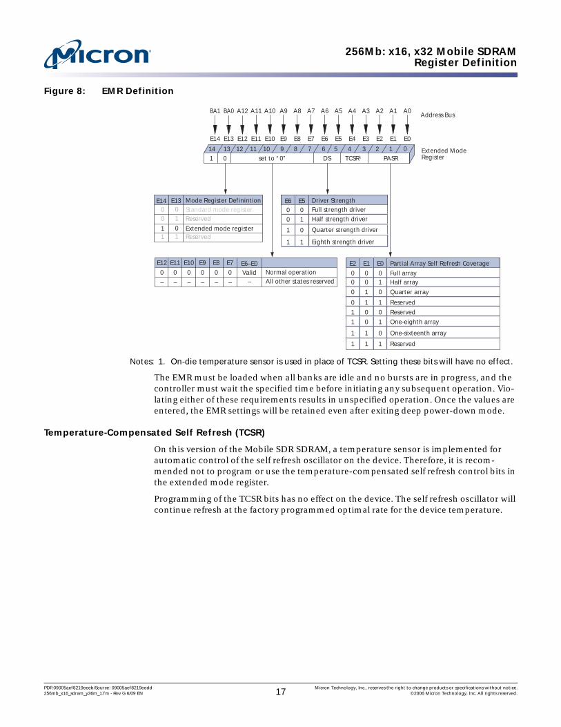
Extended Mode Register (EMR)
The low-power EMR controls the functions beyond those controlled by the mode regis-ter. These additional functions are special features of the mobile device. They include temperature-compensated self refresh (TCSR) control, partial-array self refresh (PASR), and output drive strength.
The low-power EMR is programmed via the MODE REGISTER SET command and retains the stored information until it is programmed again or the device loses power.
CLK
DQ
T2 T1 T3 T0
CL = 3
LZ
DOUT
t OH t
COMMAND NOP READ
t AC
T4
NOP
DON’T CARE
UNDEFINED
CLK
DQ
T2 T1 T3 T0
CL = 2
LZ
DOUT
t OH t
COMMAND NOP READ
t AC
NOP
NOP
PDF:09005aef8219eeeb/Source: 09005aef8219eedd Micron Technology, Inc., reserves the right to change products or specifications without notice.256mb_x16_sdram_y36m_1.fm - Rev G 6/09 EN 16 ©2006 Micron Technology, Inc. All rights reserved.
256Mb: x16, x32 Mobile SDRAMRegister Definition
Figure 8: EMR Definition
Notes: 1. On-die temperature sensor is used in place of TCSR. Setting these bits will have no effect.
The EMR must be loaded when all banks are idle and no bursts are in progress, and the controller must wait the specified time before initiating any subsequent operation. Vio-lating either of these requirements results in unspecified operation. Once the values are entered, the EMR settings will be retained even after exiting deep power-down mode.
Temperature-Compensated Self Refresh (TCSR)
On this version of the Mobile SDR SDRAM, a temperature sensor is implemented for automatic control of the self refresh oscillator on the device. Therefore, it is recom-mended not to program or use the temperature-compensated self refresh control bits in the extended mode register.
Programming of the TCSR bits has no effect on the device. The self refresh oscillator will continue refresh at the factory programmed optimal rate for the device temperature.
Extended Mode Register
Address Bus
9 7 6 5 4 3 8 2 1 PASR TCSR1DS set to “0” 0
E12
A11
E11
A10
E10
A9
E9
A8
E8
A7
E7
A6
E6
A5
E5
A4
E4
A3
E3
A2
E2
A1
E1
A0
E0
10 11 12
E2
0 0
0
0
1
1
1
1
E1
0 0
1
1
0
0
1
1
E0
0 1
0
1
0
1
0
1
Partial Array Self Refresh Coverage
Full arrayHalf array
Quarter array
Reserved
Reserved
One-eighth array
One-sixteenth array
Reserved
E6 0 0
1
E5 0 1
0
Driver Strength Full strength driver Half strength driver
Quarter strength driver
BA0 A12
E13
BA1
E14
1 13 14
0 0
1 1
Mode Register Definintion Standard mode register Reserved
Extended mode register Reserved
E14 0 1
0 1
E13
0
E11
0
–
E12
0
–
E10
0
–
E9
0
–
E8
0
–
E7
0
–Valid
– Normal operation All other states reserved
1 1 Eighth strength driver
E6–E0
PDF:09005aef8219eeeb/Source: 09005aef8219eedd Micron Technology, Inc., reserves the right to change products or specifications without notice.256mb_x16_sdram_y36m_1.fm - Rev G 6/09 EN 17 ©2006 Micron Technology, Inc. All rights reserved.

256Mb: x16, x32 Mobile SDRAMRegister Definition
Partial-Array Self Refresh (PASR)
For further power savings during self refresh, the partial-array self refresh (PASR) feature allows the controller to select the amount of memory that will be refreshed during self refresh. The following refresh options are available.1. All banks (banks 0, 1, 2, and 3).2. Two banks (banks 0 and 1; BA1 = 0).3. One bank (bank 0; BA1 = BA0 = 0).4. Half bank (bank 0; BA1 = BA0 = row address MSB = 0).5. Quarter bank (bank 0; BA1 = BA0; row address MSB = row address MSB -1 = 0).
WRITE and READ commands occur to any bank selected during standard operation, but only the selected banks in PASR will be refreshed during self refresh. It is important to note that data in banks 2 and 3 will be lost when the two-bank option is used.
Driver StrengthBits E5 and E6 of the EMR can be used to select the driver strength of the DQ outputs. This value should be set according to the application’s requirements.
PDF:09005aef8219eeeb/Source: 09005aef8219eedd Micron Technology, Inc., reserves the right to change products or specifications without notice.256mb_x16_sdram_y36m_1.fm - Rev G 6/09 EN 18 ©2006 Micron Technology, Inc. All rights reserved.

256Mb: x16, x32 Mobile SDRAMCommands
CommandsTable 5 provides a quick reference of available commands. This is followed by a written description of each command. Three additional truth tables appear following “Opera-tions” on page 23. These tables provide current state/next state information.
Notes: 1. CKE is HIGH for all commands shown except SELF REFRESH and deep power-down.2. All states and sequences not shown are reserved and/or illegal.3. The purpose of the BURST TERMINATE command is to stop a data burst, thus the command
could coincide with data on the bus. However, the DQs column reads a don’t care state to illustrate that the BURST TERMINATE command can occur when there is no data present.
4. DESELECT and NOP are functionally interchangeable.5. BA[1:0] provide bank address and A[12:0] provide row address.6. BA[1:0] provide bank address; A[9:0] provide column address; A10 HIGH enables the auto
precharge feature (nonpersistent), and A10 LOW disables the auto precharge feature.7. Applies only to read bursts with auto precharge disabled; this command is undefined (and
should not be used) for READ bursts with auto precharge enabled and for WRITE bursts.8. This command is a BURST TERMINATE if CKE is HIGH, deep power-down if CKE is LOW.9. A10 LOW: BA[1:0] determine which bank is precharged. A10 HIGH: all banks are pre-
charged and BA[1:0] are “Don’t Care.”10. This command is AUTO REFRESH if CKE is HIGH, SELF REFRESH if CKE is LOW.11. Internal refresh counter controls row addressing; all inputs and I/Os are “Don’t Care”
except for CKE.12. BA[1:0] select either the standard mode register or the extended mode register (BA0 = 0,
BA1 = 0 select the standard mode register; BA0 = 0, BA1 = 1 select extended mode register; other combinations of BA[1:0] are reserved.) A[12:0] provide the op-code to be written to the selected mode register.
COMMAND INHIBIT
The COMMAND INHIBIT function prevents new commands from being executed by the SDRAM, regardless of whether the CLK signal is enabled. The SDRAM is effectively dese-lected. Operations already in progress are not affected.
Table 5: Truth Table – Commands and DQM OperationNotes 1 and 2 apply to all commands
Name (Function) CS# RAS# CAS# WE# DQM ADDR DQs Notes
COMMAND INHIBIT (NOP) H X X X X X X 4
NO OPERATION (NOP) L H H H X X X 4
ACTIVE (Select bank and activate row) L L H H X Bank/Row X 5
READ (Select bank and column, and start READ burst) L H L H L/H Bank/Col X 6
WRITE (Select bank and column, and start WRITE burst) L H L L L/H Bank/Col Valid 6
BURST TERMINATE or deep power-down(Enter deep power-down mode)
L H H L X X X 3, 7, 8
PRECHARGE (Deactivate row in bank or banks) L L H L X Code X 9
AUTO REFRESH or SELF REFRESH(Enter self refresh mode)
L L L H X X X 10, 11
LOAD MODE REGISTER L L L L X Op-Code X 12
Write enable/output enable X X X X L X Active
Write inhibit/output High-Z X X X X H X High-Z
PDF:09005aef8219eeeb/Source: 09005aef8219eedd Micron Technology, Inc., reserves the right to change products or specifications without notice.256mb_x16_sdram_y36m_1.fm - Rev G 6/09 EN 19 ©2006 Micron Technology, Inc. All rights reserved.
256Mb: x16, x32 Mobile SDRAMCommands
NO OPERATION (NOP)
The NO OPERATION (NOP) command is used to perform a NOP to an SDRAM which is selected (CS# is LOW). This prevents unwanted commands from being registered during idle or wait states. Operations already in progress are not affected.
LOAD MODE REGISTER (LMR)
The mode register is loaded via inputs A[12:0] and BA[1:0]. (See “Mode Register” on page 13.) The LMR and LOAD EXTENDED MODE REGISTER (LEMR) commands can only be issued when all banks are idle, and a subsequent executable command cannot be issued until tMRD is met.
ACTIVE
The ACTIVE command is used to open (or activate) a row in a particular bank for a sub-sequent access. The value on the BA[1:0] inputs selects the bank, and the address pro-vided selects the row. This row remains active (or open) for accesses until a PRECHARGE command is issued to that bank. A PRECHARGE command must be issued before open-ing a different row in the same bank.
READ
The READ command is used to initiate a burst read access to an active row. The value on the BA[1:0] inputs selects the bank, and the address provided selects the starting column location. The value on input A10 determines whether or not auto precharge is used. If auto precharge is selected, the row being accessed will be precharged at the end of the read burst; if auto precharge is not selected, the row will remain open for subsequent accesses. Read data appears on the DQs subject to the logic level on the DQM inputs two clocks earlier. If a given DQM signal was registered HIGH, the corresponding DQs will be High-Z two clocks later; if the DQM signal was registered LOW, the DQs will provide valid data.
WRITE
The WRITE command is used to initiate a burst write access to an active row. The value on the BA[1:0] inputs selects the bank, and the address provides the starting column location. The value on input A10 determines whether or not auto precharge is used. If auto precharge is selected, the row being accessed will be precharged at the end of the write burst; if auto precharge is not selected, the row will remain open for subsequent accesses. Input data appearing on the DQs is written to the memory array subject to the DQM input logic level appearing coincident with the data. If a given DQM signal is regis-tered LOW, the corresponding data will be written to memory; if the DQM signal is regis-tered HIGH, the corresponding data inputs will be ignored, and a write will not be executed to that byte/column location.
PRECHARGE
The PRECHARGE command is used to deactivate the open row in a particular bank or the open row in all banks. The bank(s) will be available for a subsequent row access a specified time (tRP) after the precharge command is issued. Input A10 determines whether one or all banks are to be precharged, and in the case where only one bank is to be precharged, inputs BA[1:0] select the bank. Otherwise BA[1:0] are treated as “Don’t Care.” Once a bank has been precharged, it is in the idle state and must be activated prior to any READ or WRITE commands being issued to that bank.
PDF:09005aef8219eeeb/Source: 09005aef8219eedd Micron Technology, Inc., reserves the right to change products or specifications without notice.256mb_x16_sdram_y36m_1.fm - Rev G 6/09 EN 20 ©2006 Micron Technology, Inc. All rights reserved.

256Mb: x16, x32 Mobile SDRAMCommands
BURST TERMINATE
The BURST TERMINATE command is used to truncate either fixed-length or continuous page bursts. The most recently registered READ or WRITE command prior to the BURST TERMINATE command will be truncated, as shown in “Operations” on page 23.
AUTO REFRESH
AUTO REFRESH is used during normal operation of the SDRAM and is analogous to CAS#-BEFORE-RAS# (CBR) refresh in conventional DRAM. This command is non persis-tent, so it must be issued each time a refresh is required. All active banks must be PRE-CHARGED prior to issuing an AUTO REFRESH command. The AUTO REFRESH command should not be issued until the minimum tRP has been met after the PRE-CHARGE command, as shown in “Operations” on page 23.
The addressing is generated by the internal refresh controller. This makes the address bits “Don’t Care” during an AUTO REFRESH command. The 256Mb SDRAM requires 8192 AUTO REFRESH cycles every 64ms (tREF). Providing a distributed AUTO REFRESH command every 7.8125µs will meet the refresh requirement and ensure that each row is refreshed. Alternatively, 8192 AUTO REFRESH commands can be issued in a burst at the minimum cycle rate (tRFC), once every 64ms.
SELF REFRESH
The SELF REFRESH command can be used to retain data in the SDRAM, even if the rest of the system is powered down. When in the self refresh mode, the SDRAM retains data without external clocking. The SELF REFRESH command is initiated like an AUTO REFRESH command, except CKE is disabled (LOW). Once the SELF REFRESH command is registered, all the inputs to the SDRAM become “Don’t Care” with the exception of CKE, which must remain LOW.
Once self refresh mode is engaged, the SDRAM provides its own internal clocking, caus-ing it to perform its own auto refresh cycles. The SDRAM must remain in self refresh mode for a minimum period equal to tRAS and may remain in self refresh mode for an indefinite period beyond that.
The procedure for exiting self refresh requires a sequence of commands. First, CLK must be stable (stable clock is defined as a signal cycling within timing constraints specified for the clock ball) prior to CKE going back HIGH. Once CKE is HIGH, the SDRAM must have NOP commands issued (a minimum of two clocks) for tXSR because time is required for the completion of any internal refresh in progress.
Upon exiting the self refresh mode, AUTO REFRESH commands must be issued every 7.8125µs or less as both SELF REFRESH and AUTO REFRESH utilize the row refresh counter.
Auto Precharge
Auto precharge is a feature which performs the same individual-bank precharge func-tion described above, without requiring an explicit command. This is accomplished by using A10 to enable auto precharge in conjunction with a specific READ or WRITE com-mand. A precharge of the bank/row that is addressed with the READ or WRITE com-mand is automatically performed upon completion of the READ or WRITE burst, except in the continuous page burst mode, where auto precharge does not apply. Auto pre-charge is non persistent in that it is either enabled or disabled for each individual READ or WRITE command.
PDF:09005aef8219eeeb/Source: 09005aef8219eedd Micron Technology, Inc., reserves the right to change products or specifications without notice.256mb_x16_sdram_y36m_1.fm - Rev G 6/09 EN 21 ©2006 Micron Technology, Inc. All rights reserved.

256Mb: x16, x32 Mobile SDRAMCommands
Auto precharge ensures that the precharge is initiated at the earliest valid stage within a burst. The user must not issue another command to the same bank until the precharge time (tRP) is completed. This is determined as if an explicit PRECHARGE command was issued at the earliest possible time, as described for each burst type in “Operations” on page 23.
Deep Power-Down
Deep power-down is an operating mode used to achieve maximum power reduction by eliminating the power to the memory array. Data will not be retained once the device enters deep power-down mode.
PDF:09005aef8219eeeb/Source: 09005aef8219eedd Micron Technology, Inc., reserves the right to change products or specifications without notice.256mb_x16_sdram_y36m_1.fm - Rev G 6/09 EN 22 ©2006 Micron Technology, Inc. All rights reserved.
256Mb: x16, x32 Mobile SDRAMOperations
Operations
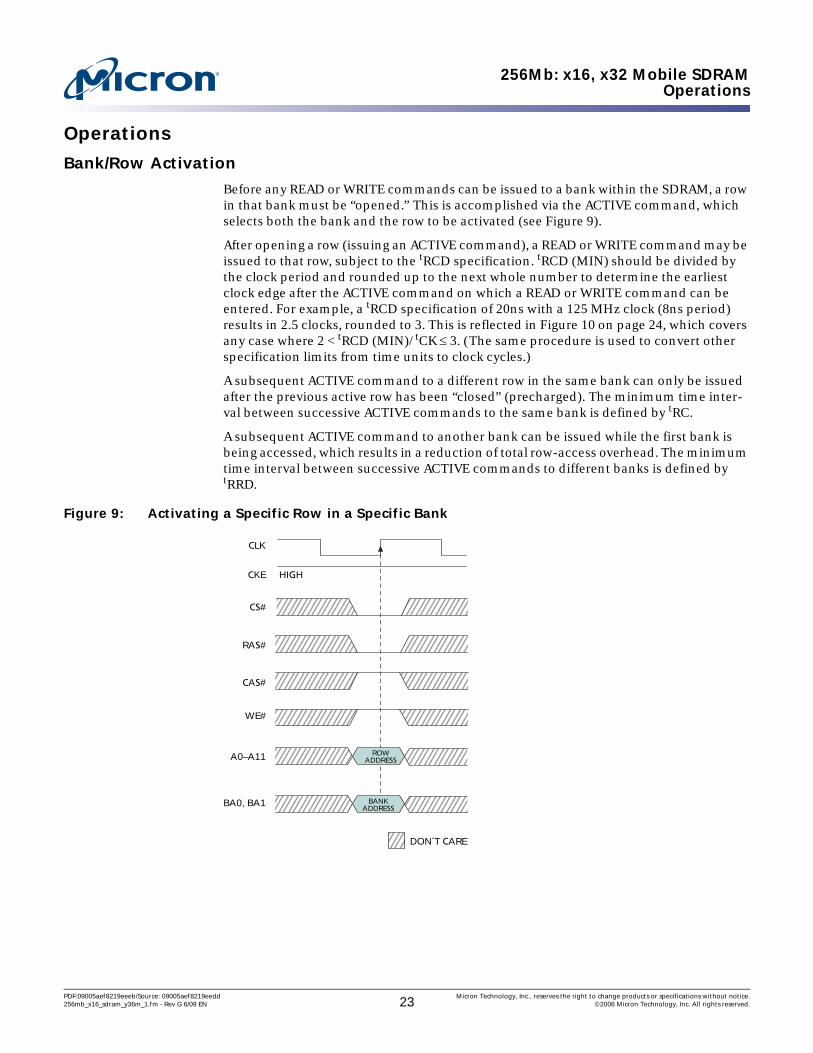
Bank/Row Activation
Before any READ or WRITE commands can be issued to a bank within the SDRAM, a row in that bank must be “opened.” This is accomplished via the ACTIVE command, which selects both the bank and the row to be activated (see Figure 9).
After opening a row (issuing an ACTIVE command), a READ or WRITE command may be issued to that row, subject to the tRCD specification. tRCD (MIN) should be divided by the clock period and rounded up to the next whole number to determine the earliest clock edge after the ACTIVE command on which a READ or WRITE command can be entered. For example, a tRCD specification of 20ns with a 125 MHz clock (8ns period) results in 2.5 clocks, rounded to 3. This is reflected in Figure 10 on page 24, which covers any case where 2 < tRCD (MIN)/tCK ≤ 3. (The same procedure is used to convert other specification limits from time units to clock cycles.)
A subsequent ACTIVE command to a different row in the same bank can only be issued after the previous active row has been “closed” (precharged). The minimum time inter-val between successive ACTIVE commands to the same bank is defined by tRC.
A subsequent ACTIVE command to another bank can be issued while the first bank is being accessed, which results in a reduction of total row-access overhead. The minimum time interval between successive ACTIVE commands to different banks is defined by tRRD.
Figure 9: Activating a Specific Row in a Specific Bank
CS#
WE#
CAS#
RAS#
CKE
CLK
A0–A11 ROWADDRESS
DON´T CARE
HIGH
BA0, BA1 BANKADDRESS
PDF:09005aef8219eeeb/Source: 09005aef8219eedd Micron Technology, Inc., reserves the right to change products or specifications without notice.256mb_x16_sdram_y36m_1.fm - Rev G 6/09 EN 23 ©2006 Micron Technology, Inc. All rights reserved.

256Mb: x16, x32 Mobile SDRAMOperations
Figure 10: Example: Meeting tRCD (MIN) When 2 < tRCD (MIN)/tCK < 3
READs
READ bursts are initiated with a READ command, as shown in Figure 11.
The starting column and bank addresses are provided with the READ command, and auto precharge is either enabled or disabled for that burst access. If auto precharge is enabled, the row being accessed is precharged at the completion of the burst. For the generic READ commands used in the following illustrations, auto precharge is disabled.
During READ bursts, the valid data-out element from the starting column address will be available following the CL after the READ command. Each subsequent data-out ele-ment will be valid by the next positive clock edge. Figure 7 on page 16 shows general tim-ing for each possible CL setting.
Figure 11: READ Command
CLK
T2T1 T3T0
t
COMMAND NOPACTIVE READ or WRITE
NOP
RCD (MIN)
tCK tCK tCK
DON’T CARE
CS#
WE#
CAS#
RAS#
CKE
CLK
COLUMNADDRESS
A10
BA0, BA1
DON’T CARE
HIGH
ENABLE AUTO PRECHARGE
DISABLE AUTO PRECHARGE
BANKADDRESS
A0–A8
A9, A11
PDF:09005aef8219eeeb/Source: 09005aef8219eedd Micron Technology, Inc., reserves the right to change products or specifications without notice.256mb_x16_sdram_y36m_1.fm - Rev G 6/09 EN 24 ©2006 Micron Technology, Inc. All rights reserved.
256Mb: x16, x32 Mobile SDRAMOperations
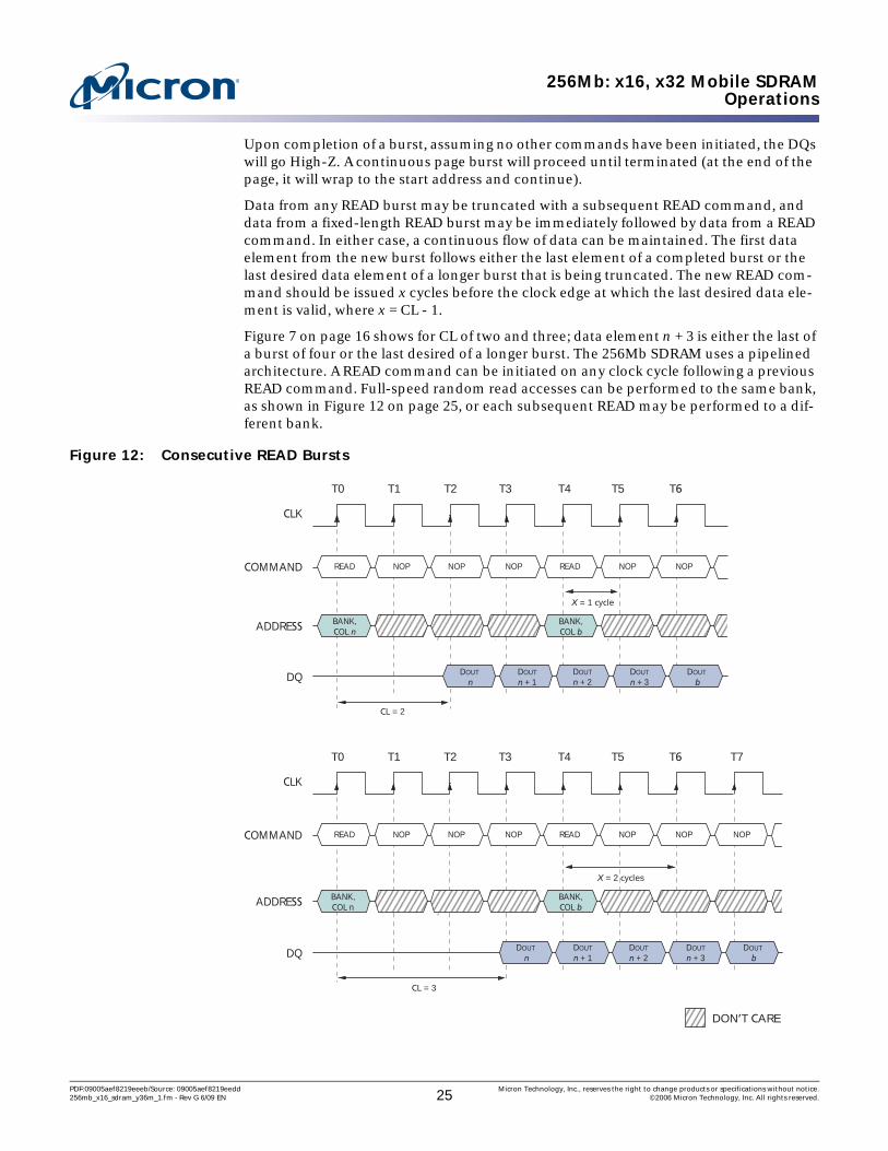
Upon completion of a burst, assuming no other commands have been initiated, the DQs will go High-Z. A continuous page burst will proceed until terminated (at the end of the page, it will wrap to the start address and continue).
Data from any READ burst may be truncated with a subsequent READ command, and data from a fixed-length READ burst may be immediately followed by data from a READ command. In either case, a continuous flow of data can be maintained. The first data element from the new burst follows either the last element of a completed burst or the last desired data element of a longer burst that is being truncated. The new READ com-mand should be issued x cycles before the clock edge at which the last desired data ele-ment is valid, where x = CL - 1.
Figure 7 on page 16 shows for CL of two and three; data element n + 3 is either the last of a burst of four or the last desired of a longer burst. The 256Mb SDRAM uses a pipelined architecture. A READ command can be initiated on any clock cycle following a previous READ command. Full-speed random read accesses can be performed to the same bank, as shown in Figure 12 on page 25, or each subsequent READ may be performed to a dif-ferent bank.
Figure 12: Consecutive READ Bursts
CLK
DQ DOUT n
T2 T1 T4 T3 T6 T5 T0
COMMAND
ADDRESS
READ NOP NOP NOP NOP
BANK, COL n
NOP
BANK, COL b
DOUT n + 1
DOUT n + 2
DOUT
n + 3DOUT
b
READ
X = 1 cycle
CL = 2
CLK
DQ DOUT n
T2 T1 T4 T3 T6 T5 T0
COMMAND
ADDRESS
READ NOP NOP NOP NOP
BANK, COL n
NOP
BANK, COL b
DOUT n + 1
DOUT n + 2
DOUT n + 3
DOUT b
READ NOP
T7
X = 2 cycles
CL = 3
DON’T CARE
PDF:09005aef8219eeeb/Source: 09005aef8219eedd Micron Technology, Inc., reserves the right to change products or specifications without notice.256mb_x16_sdram_y36m_1.fm - Rev G 6/09 EN 25 ©2006 Micron Technology, Inc. All rights reserved.
256Mb: x16, x32 Mobile SDRAMOperations
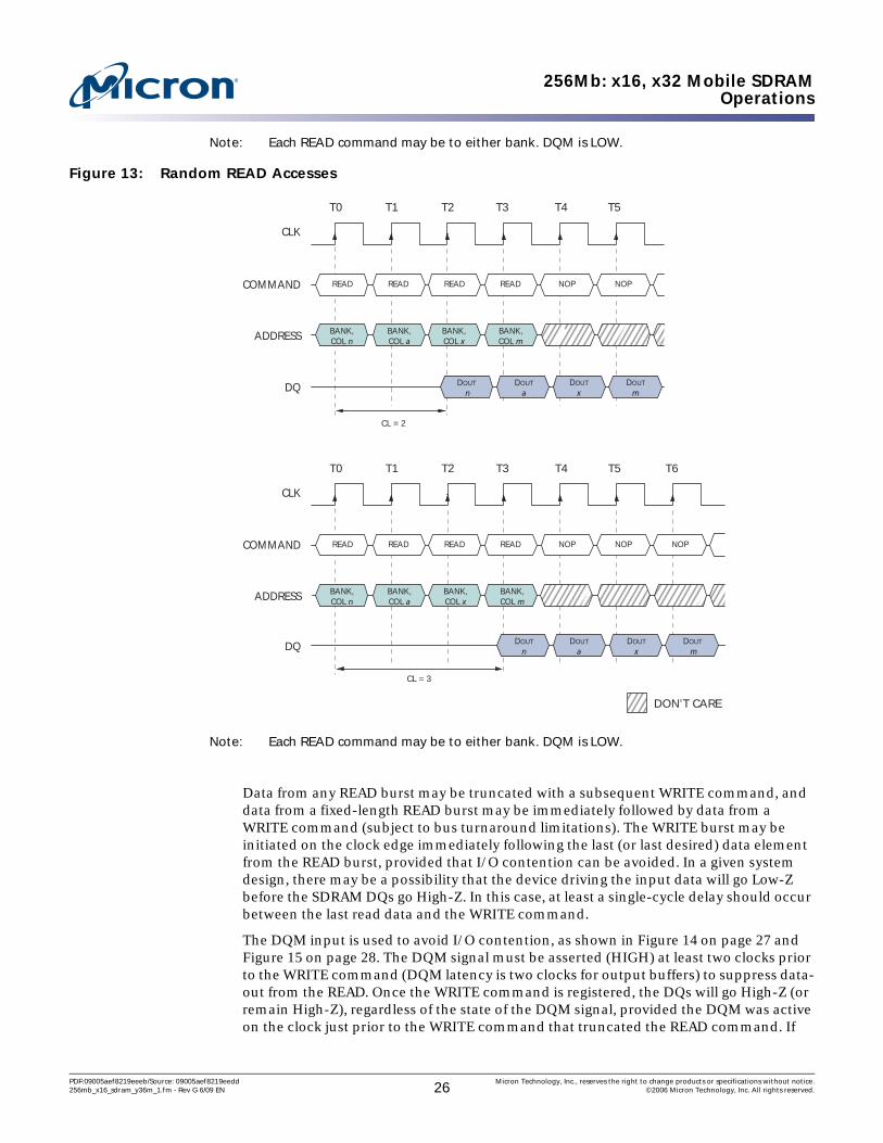
Note: Each READ command may be to either bank. DQM is LOW.
Figure 13: Random READ Accesses
Note: Each READ command may be to either bank. DQM is LOW.
Data from any READ burst may be truncated with a subsequent WRITE command, and data from a fixed-length READ burst may be immediately followed by data from a WRITE command (subject to bus turnaround limitations). The WRITE burst may be initiated on the clock edge immediately following the last (or last desired) data element from the READ burst, provided that I/O contention can be avoided. In a given system design, there may be a possibility that the device driving the input data will go Low-Z before the SDRAM DQs go High-Z. In this case, at least a single-cycle delay should occur between the last read data and the WRITE command.
The DQM input is used to avoid I/O contention, as shown in Figure 14 on page 27 and Figure 15 on page 28. The DQM signal must be asserted (HIGH) at least two clocks prior to the WRITE command (DQM latency is two clocks for output buffers) to suppress data-out from the READ. Once the WRITE command is registered, the DQs will go High-Z (or remain High-Z), regardless of the state of the DQM signal, provided the DQM was active on the clock just prior to the WRITE command that truncated the READ command. If
CLK
DQ
T2 T1 T4 T3 T6 T5 T0
COMMAND
ADDRESS
READ NOP NOP
BANK, COL n
DON’T CARE
DOUT n
DOUT a
DOUT x
DOUT m
READ READ READ NOP
BANK, COL a
BANK,COL x
BANK,COL m
CLK
DQ DOUT n
T2 T1 T4 T3 T5 T0
COMMAND
ADDRESS
READ NOP
BANK, COL n
DOUT a
DOUT x
DOUT m
READ READ READ NOP
BANK, COL a
BANK, COL x
BANK, COL m
CL = 2
CL = 3
PDF:09005aef8219eeeb/Source: 09005aef8219eedd Micron Technology, Inc., reserves the right to change products or specifications without notice.256mb_x16_sdram_y36m_1.fm - Rev G 6/09 EN 26 ©2006 Micron Technology, Inc. All rights reserved.

256Mb: x16, x32 Mobile SDRAMOperations
not, the second WRITE will be an invalid WRITE. For example, if DQM was LOW during T4 (as in Figure 15 on page 28) then the WRITEs at T5 and T7 would be valid, while the WRITE at T6 would be invalid.
The DQM signal must be de-asserted prior to the WRITE command (DQM latency is zero clocks for input buffers) to ensure that the written data is not masked. Figure 12 on page 25 shows the case where the clock frequency allows for bus contention to be avoided without adding a NOP cycle, and Figure 13 on page 26 shows the case where the additional NOP is needed.
A fixed-length READ burst may be followed by, or truncated with, a PRECHARGE com-mand to the same bank (provided that auto precharge was not activated). The PRE-CHARGE command should be issued x cycles before the clock edge at which the last desired data element is valid, where x = CL - 1. This is shown in Figure 16 on page 28 for each possible CL; data element n + 3 is either the last of a burst of four or the last desired of a longer burst. Following the PRECHARGE command, a subsequent command to the same bank cannot be issued until tRP is met. Note that part of the row precharge time is hidden during the access of the last data element(s).
In the case of a fixed-length burst being executed to completion, a PRECHARGE com-mand issued at the optimum time (as described above) provides the same operation that would result from the same fixed-length burst with auto precharge. The disadvan-tage of the PRECHARGE command is that it requires that the command and address buses be available at the appropriate time to issue the command; the advantage of the PRECHARGE command is that it can be used to truncate fixed-length or continuous page bursts.
Figure 14: READ-to-WRITE
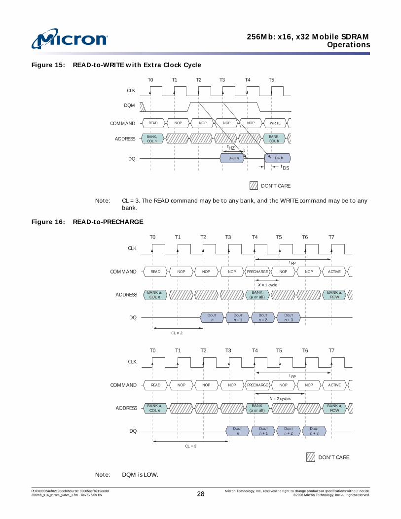
Note: CL = 3. The READ command may be to any bank, and the WRITE command may be to any bank. If a burst of one is used, then DQM is not required.
DON’T CARE
READ NOP NOP WRITE NOP
CLK
T2 T1 T4 T3 T0
DQM
DQ DOUT n
COMMAND
DIN b
ADDRESS BANK, COL n
BANK, COL b
DS
t HZ
t
t CK
PDF:09005aef8219eeeb/Source: 09005aef8219eedd Micron Technology, Inc., reserves the right to change products or specifications without notice.256mb_x16_sdram_y36m_1.fm - Rev G 6/09 EN 27 ©2006 Micron Technology, Inc. All rights reserved.
256Mb: x16, x32 Mobile SDRAMOperations
Figure 15: READ-to-WRITE with Extra Clock Cycle
Note: CL = 3. The READ command may be to any bank, and the WRITE command may be to any bank.
Figure 16: READ-to-PRECHARGE
Note: DQM is LOW.
DON’T CARE
READ NOP NOP NOP NOP
DQM
CLK
DQ DOUT n
T2 T1 T4 T3 T0
COMMAND
ADDRESS BANK, COL n
WRITE
DIN b
BANK, COL b
T5
DS
t HZ
t
CLK
DQ DOUT n
T2 T1 T4 T3 T6 T5 T0
COMMAND
ADDRESS
READ NOP NOP NOP NOP NOP
DOUT n + 1
DOUT n + 2
DOUT n + 3
PRECHARGE ACTIVE
t RP
T7
CLK
DQ DOUT n
T2 T1 T4 T3 T6 T5 T0
COMMAND
ADDRESS
READ NOP NOP NOP NOP NOP
DOUT n + 1
DOUT n + 2
DOUT n + 3
PRECHARGE ACTIVE
t RP
T7
DON’T CARE
X = 1 cycle
CL = 2
CL = 3
BANK a, COL n
BANK a, ROW
BANK (a or all)
BANK a, COL n
BANK a, ROW
BANK (a or all)
X = 2 cycles
PDF:09005aef8219eeeb/Source: 09005aef8219eedd Micron Technology, Inc., reserves the right to change products or specifications without notice.256mb_x16_sdram_y36m_1.fm - Rev G 6/09 EN 28 ©2006 Micron Technology, Inc. All rights reserved.
256Mb: x16, x32 Mobile SDRAMOperations
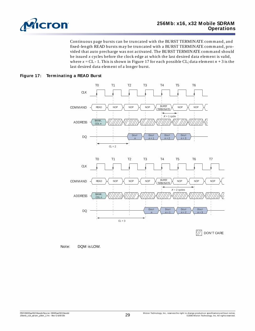
Continuous page bursts can be truncated with the BURST TERMINATE command, and fixed-length READ bursts may be truncated with a BURST TERMINATE command, pro-vided that auto precharge was not activated. The BURST TERMINATE command should be issued x cycles before the clock edge at which the last desired data element is valid, where x = CL - 1. This is shown in Figure 17 for each possible CL; data element n + 3 is the last desired data element of a longer burst.
Figure 17: Terminating a READ Burst
Note: DQM is LOW.
DON’T CARE
CLK
DQ DOUT n
T2 T1 T4 T3 T6 T5 T0
COMMAND
ADDRESS
READ NOP NOP NOP NOP
BANK, COL n
NOP
DOUT n + 1
DOUT n + 2
DOUT n + 3
BURST TERMINATE
NOP
T7
CLK
DQ DOUT n
T2 T1 T4 T3 T6 T5 T0
COMMAND
ADDRESS
READ NOP NOP NOP
BANK, COL n
NOP
DOUT n + 1
DOUT n + 2
DOUT n + 3
BURST TERMINATE
NOP
X = 1 cycle
CL = 2
CL = 3
X = 2 cycles
PDF:09005aef8219eeeb/Source: 09005aef8219eedd Micron Technology, Inc., reserves the right to change products or specifications without notice.256mb_x16_sdram_y36m_1.fm - Rev G 6/09 EN 29 ©2006 Micron Technology, Inc. All rights reserved.
256Mb: x16, x32 Mobile SDRAMOperations
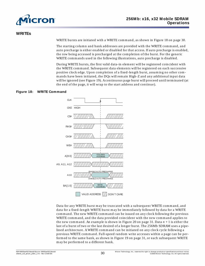
WRITEs
WRITE bursts are initiated with a WRITE command, as shown in Figure 18 on page 30.
The starting column and bank addresses are provided with the WRITE command, and auto precharge is either enabled or disabled for that access. If auto precharge is enabled, the row being accessed is precharged at the completion of the burst. For the generic WRITE commands used in the following illustrations, auto precharge is disabled.
During WRITE bursts, the first valid data-in element will be registered coincident with the WRITE command. Subsequent data elements will be registered on each successive positive clock edge. Upon completion of a fixed-length burst, assuming no other com-mands have been initiated, the DQs will remain High-Z and any additional input data will be ignored (see Figure 19). A continuous page burst will proceed until terminated (at the end of the page, it will wrap to the start address and continue).
Figure 18: WRITE Command
Data for any WRITE burst may be truncated with a subsequent WRITE command, and data for a fixed-length WRITE burst may be immediately followed by data for a WRITE command. The new WRITE command can be issued on any clock following the previous WRITE command, and the data provided coincident with the new command applies to the new command. An example is shown in Figure 20 on page 31. Data n + 1 is either the last of a burst of two or the last desired of a longer burst. The 256Mb SDRAM uses a pipe-lined architecture. A WRITE command can be initiated on any clock cycle following a previous WRITE command. Full-speed random write accesses within a page can be per-formed to the same bank, as shown in Figure 19 on page 31, or each subsequent WRITE may be performed to a different bank.
CS#
WE#
CAS#
RAS#
CKE
CLK
COLUMN ADDRESS
DON’T CARE
HIGH
ENABLE AUTO PRECHARGE
DISABLE AUTO PRECHARGE
BANK ADDRESS
A[8:0]
A10
BA[1:0]
A9, A11, A12
VALID ADDRESS
PDF:09005aef8219eeeb/Source: 09005aef8219eedd Micron Technology, Inc., reserves the right to change products or specifications without notice.256mb_x16_sdram_y36m_1.fm - Rev G 6/09 EN 30 ©2006 Micron Technology, Inc. All rights reserved.

256Mb: x16, x32 Mobile SDRAMOperations
Figure 19: WRITE Burst
Note: BL = 2. DQM is LOW.
Figure 20: WRITE-to-WRITE
Note: BL = 2. DQM is LOW. Each WRITE command may be to any bank.
Data for any WRITE burst may be truncated with a subsequent READ command, and data for a fixed-length WRITE burst may be immediately followed by a READ command. Once the READ command is registered, the data inputs will be ignored, and WRITEs will not be executed. An example is shown in Figure 21 on page 32. Data n + 1 is either the last of a burst of two or the last desired of a longer burst.
Data for a fixed-length WRITE burst may be followed by, or truncated with, a PRE-CHARGE command to the same bank (provided that auto precharge was not activated), and a continuous page WRITE burst can be truncated with a PRECHARGE command to the same bank. The PRECHARGE command should be issued tWR after the clock edge at which the last desired input data element is registered. The auto precharge mode requires a tWR of at least one clock plus time (see note 24 on page 53), regardless of fre-quency.
In addition, when truncating a WRITE burst, the DQM signal must be used to mask input data for the clock edge prior to, and the clock edge coincident with, the PRE-CHARGE command. An example is shown in Figure 21 on page 32. Data n + 1 is either the last of a burst of two or the last desired of a longer burst. Following the PRECHARGE command, a subsequent command to the same bank cannot be issued until tRP is met.
CLK
DQ DIN
n
T2 T1 T3 T0
COMMAND
ADDRESS
NOP NOP
DON’T CARE
WRITE
DIN n + 1
NOP
BANK, COL n
CLK
DQ
T2 T1 T0
COMMAND
ADDRESS
NOP WRITE WRITE
BANK, COL n
BANK, COL b
DIN
n DIN
n + 1 DIN b
DON’T CARE
PDF:09005aef8219eeeb/Source: 09005aef8219eedd Micron Technology, Inc., reserves the right to change products or specifications without notice.256mb_x16_sdram_y36m_1.fm - Rev G 6/09 EN 31 ©2006 Micron Technology, Inc. All rights reserved.

256Mb: x16, x32 Mobile SDRAMOperations
In the case of a fixed-length burst being executed to completion, a PRECHARGE com-mand issued at the optimum time (as described above) provides the same operation that would result from the same fixed-length burst with auto precharge. The disadvan-tage of the PRECHARGE command is that it requires that the command and address buses be available at the appropriate time to issue the command; the advantage of the PRECHARGE command is that it can be used to truncate fixed-length or continuous page bursts.
Figure 21: Random WRITE Cycles
Note: Each WRITE command may be to any bank. DQM is LOW.
Figure 22: WRITE-to-READ
Note: BL = 2. The WRITE command may be to any bank, and the READ command may be to any bank. DQM is LOW. CL = 2 for illustration.
DON’T CARE
CLK
DQ DIN
n
T2 T1 T3 T0
COMMAND
ADDRESS
WRITE
BANK, COL n
DIN a
DIN x
DIN m
WRITE WRITE WRITE
BANK, COL a
BANK, COL x
BANK, COL m
DON’T CARE
CLK
DQ
T2 T1 T3 T0
COMMAND
ADDRESS
NOP WRITE
BANK, COL n
DIN n
DIN n + 1
DOUT
b
READ NOP NOP
BANK, COL b
NOP
DOUT
b + 1
T4 T5
PDF:09005aef8219eeeb/Source: 09005aef8219eedd Micron Technology, Inc., reserves the right to change products or specifications without notice.256mb_x16_sdram_y36m_1.fm - Rev G 6/09 EN 32 ©2006 Micron Technology, Inc. All rights reserved.

256Mb: x16, x32 Mobile SDRAMOperations
Figure 23: WRITE-to-PRECHARGE
Note: DQM could remain LOW in this example if the WRITE burst is a fixed length of two.
Figure 24: Terminating a WRITE Burst
Note: DQMs are LOW.
DON’T CARE
DQM
CLK
DQ
T2 T1 T4 T3 T0
COMMAND
ADDRESS BANK a, COL n
T5
NOP WRITE PRECHARGE NOP NOP
DIN n
DIN n + 1
ACTIVE
t RP
BANK (a or all)
t WR
BANK a, ROW
DQM
DQ
COMMAND
ADDRESS BANK a, COL n
NOP WRITE PRECHARGE NOP NOP
DIN n
DIN n + 1
ACTIVE
t RP
BANK (a or all)
t WR
BANK a, ROW
T6
NOP
NOP
tWR@ tCK < 15ns
tWR@ tCK ≥ 15ns
DON’T CARE
CLK
DQ
T2 T1 T0
COMMAND
ADDRESS BANK, COL n
WRITE BURST TERMINATE
NEXT COMMAND
DIN n
(Address)
(Data)
PDF:09005aef8219eeeb/Source: 09005aef8219eedd Micron Technology, Inc., reserves the right to change products or specifications without notice.256mb_x16_sdram_y36m_1.fm - Rev G 6/09 EN 33 ©2006 Micron Technology, Inc. All rights reserved.

256Mb: x16, x32 Mobile SDRAMOperations
Fixed-length or continuous page WRITE bursts can be truncated with the BURST TER-MINATE command. When truncating a WRITE burst, the input data applied coincident with the BURST TERMINATE command will be ignored. The last data written (provided that DQM is LOW at that time) will be the input data applied one clock previous to the BURST TERMINATE command. This is shown in Figure 22 on page 32, where data n is the last desired data element of a longer burst.
PRECHARGE
The PRECHARGE command (see Figure 25) is used to deactivate the open row in a par-ticular bank or the open row in all banks. The bank(s) will be available for a subsequent row access some specified time (tRP) after the precharge command is issued. Input A10 determines whether one or all banks are to be precharged, and in the case where only one bank is to be precharged, inputs BA[1:0] select the bank. When all banks are to be precharged, inputs BA[1:0] are treated as “Don’t Care.” Once a bank has been pre-charged, it is in the idle state and must be activated prior to any READ or WRITE com-mands being issued to that bank.
Figure 25: PRECHARGE Command
Power-Down
Power-down occurs if CKE is registered LOW coincident with a NOP or COMMAND INHIBIT when no accesses are in progress. If power-down occurs when all banks are idle, this mode is referred to as precharge power-down; if power-down occurs when there is a row active in any bank, this mode is referred to as active power-down. Entering power-down deactivates the input and output buffers, excluding CKE, for maximum power savings while in standby. The device may not remain in the power-down state longer than the refresh period (64ms) since no REFRESH operations are performed in this mode.
CS#
WE#
CAS#
RAS#
CKE
CLK
A10
DON’T CARE
HIGH
All Banks
Bank Selected
A[9:0], A11, A12
BA[1:0] BANK ADDRESS
VALID ADDRESS
PDF:09005aef8219eeeb/Source: 09005aef8219eedd Micron Technology, Inc., reserves the right to change products or specifications without notice.256mb_x16_sdram_y36m_1.fm - Rev G 6/09 EN 34 ©2006 Micron Technology, Inc. All rights reserved.

256Mb: x16, x32 Mobile SDRAMOperations
The power-down state is exited by registering a NOP or COMMAND INHIBIT and CKE HIGH at the desired clock edge (meeting tCKS). See Figure 24.
Figure 26: Power-Down
Deep Power-Down
Deep power-down mode is a maximum power savings feature achieved by shutting off the power to the entire memory array of the device. Data in the memory array will not be retained once deep power-down mode is executed. Deep power-down mode is entered by having all banks idle then CS# and WE# held LOW with RAS# and CAS# HIGH at the rising edge of the clock, while CKE is LOW. CKE must be held LOW during deep power-down.
To exit deep power-down mode, CKE must be asserted HIGH. Upon exit of Deep Power-Down mode, at least 200µs of valid clocks with either NOP or COMMAND INHIBIT com-mands are applied to the command bus, followed by a full Mobile SDRAM initialization sequence, is required.
Clock Suspend
The clock suspend mode occurs when a column access/burst is in progress and CKE is registered LOW. In the clock suspend mode, the internal clock is deactivated, “freezing” the synchronous logic.
For each positive clock edge on which CKE is sampled LOW, the next internal positive clock edge is suspended. Any command or data present on the input balls at the time of a suspended internal clock edge is ignored; any data present on the DQ balls remains driven; and burst counters are not incremented, as long as the clock is suspended. (See examples in Figure 27 and Figure 28 on page 37.)
Clock suspend mode is exited by registering CKE HIGH; the internal clock and related operation will resume on the subsequent positive clock edge.
Burst Read/Single Write
The burst read/single write mode is entered by programming the write burst mode bit (M9) in the mode register to a logic 1. In this mode, all WRITE commands result in the access of a single column location (burst of one), regardless of the programmed BL. READ commands access columns according to the programmed BL and sequence, just as in the normal mode of operation (M9 = 0).
DON’T CARE
tRAS
tRCD
tRC
All banks idleInput buffers gated off
Exit power-down mode
()()
()()
()()
tCKS > tCKS
COMMAND NOP ACTIVE
Enter power-down mode
NOP
CLK
CKE
()()
()()
PDF:09005aef8219eeeb/Source: 09005aef8219eedd Micron Technology, Inc., reserves the right to change products or specifications without notice.256mb_x16_sdram_y36m_1.fm - Rev G 6/09 EN 35 ©2006 Micron Technology, Inc. All rights reserved.
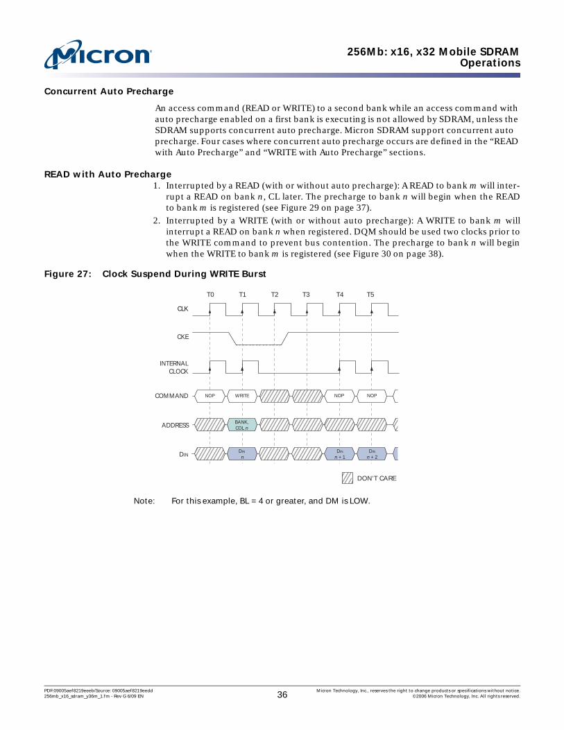
256Mb: x16, x32 Mobile SDRAMOperations
Concurrent Auto Precharge
An access command (READ or WRITE) to a second bank while an access command with auto precharge enabled on a first bank is executing is not allowed by SDRAM, unless the SDRAM supports concurrent auto precharge. Micron SDRAM support concurrent auto precharge. Four cases where concurrent auto precharge occurs are defined in the “READ with Auto Precharge” and “WRITE with Auto Precharge” sections.
READ with Auto Precharge1. Interrupted by a READ (with or without auto precharge): A READ to bank m will inter-
rupt a READ on bank n, CL later. The precharge to bank n will begin when the READto bank m is registered (see Figure 29 on page 37).
2. Interrupted by a WRITE (with or without auto precharge): A WRITE to bank m willinterrupt a READ on bank n when registered. DQM should be used two clocks prior tothe WRITE command to prevent bus contention. The precharge to bank n will beginwhen the WRITE to bank m is registered (see Figure 30 on page 38).
Figure 27: Clock Suspend During WRITE Burst
Note: For this example, BL = 4 or greater, and DM is LOW.
DON’T CARE
DIN
COMMAND
ADDRESS
WRITE
BANK, COL n
DIN
n
NOP NOP
CLK
T2 T1 T4 T3 T5 T0
CKE
INTERNAL CLOCK
NOP
DIN n + 1
DIN n + 2
PDF:09005aef8219eeeb/Source: 09005aef8219eedd Micron Technology, Inc., reserves the right to change products or specifications without notice.256mb_x16_sdram_y36m_1.fm - Rev G 6/09 EN 36 ©2006 Micron Technology, Inc. All rights reserved.
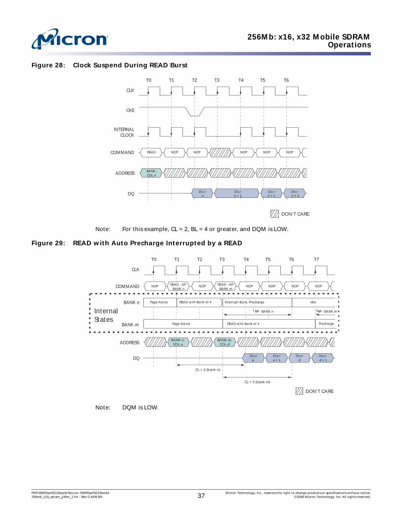
256Mb: x16, x32 Mobile SDRAMOperations
Figure 28: Clock Suspend During READ Burst
Note: For this example, CL = 2, BL = 4 or greater, and DQM is LOW.
Figure 29: READ with Auto Precharge Interrupted by a READ
Note: DQM is LOW.
DON’T CARE
CLK
DQ DOUT n
T2 T1 T4 T3 T6 T5 T0
COMMAND
ADDRESS
READ NOP NOP NOP
BANK, COL n
NOP
DOUT n + 1
DOUT n + 2
DOUT n + 3
CKE
INTERNAL CLOCK
NOP
DON’T CARE
CLK
DQ DOUT a
T2 T1 T4 T3 T6 T5 T0
COMMAND READ - AP BANK n
NOP NOP NOP NOP
DOUT a + 1
DOUT d
DOUT
d + 1
NOP
T7
BANK n
CL = 3 (bank m)
BANK m
ADDRESS
Idle
NOP
BANK n, COL a
BANK m, COL d
READ - AP BANK m
Internal States
t
Page Active READ with Burst of 4 Interrupt Burst, Precharge
Page Active READ with Burst of 4 Precharge
RP - BANK n t RP - BANK m
CL = 3 (bank n)
PDF:09005aef8219eeeb/Source: 09005aef8219eedd Micron Technology, Inc., reserves the right to change products or specifications without notice.256mb_x16_sdram_y36m_1.fm - Rev G 6/09 EN 37 ©2006 Micron Technology, Inc. All rights reserved.
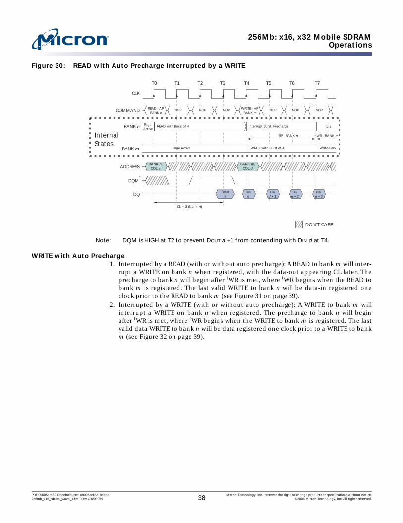
256Mb: x16, x32 Mobile SDRAMOperations
Figure 30: READ with Auto Precharge Interrupted by a WRITE
Note: DQM is HIGH at T2 to prevent DOUT a +1 from contending with DIN d at T4.
WRITE with Auto Precharge1. Interrupted by a READ (with or without auto precharge): A READ to bank m will inter-
rupt a WRITE on bank n when registered, with the data-out appearing CL later. Theprecharge to bank n will begin after tWR is met, where tWR begins when the READ tobank m is registered. The last valid WRITE to bank n will be data-in registered oneclock prior to the READ to bank m (see Figure 31 on page 39).
2. Interrupted by a WRITE (with or without auto precharge): A WRITE to bank m willinterrupt a WRITE on bank n when registered. The precharge to bank n will beginafter tWR is met, where tWR begins when the WRITE to bank m is registered. The lastvalid data WRITE to bank n will be data registered one clock prior to a WRITE to bankm (see Figure 32 on page 39).
CLK
DQ DOUT
a
T2 T1 T4 T3 T6 T5 T0
COMMAND NOP NOP NOP NOP
DIN d + 1
DIN d
DIN d + 2
DIN
d + 3
NOP
T7
BANK n
BANK m
ADDRESS
Idle
NOP
DQM
BANK n, COL a
BANK m, COL d
WRITE - AP BANK m
Internal States
t
Page Active
READ with Burst of 4 Interrupt Burst, Precharge
Page Active WRITE with Burst of 4 Write-Back
RP - BANK n t WR - BANK m
CL = 3 (bank n)
READ - AP BANK n
1
DON’T CARE
PDF:09005aef8219eeeb/Source: 09005aef8219eedd Micron Technology, Inc., reserves the right to change products or specifications without notice.256mb_x16_sdram_y36m_1.fm - Rev G 6/09 EN 38 ©2006 Micron Technology, Inc. All rights reserved.

256Mb: x16, x32 Mobile SDRAMOperations
Figure 31: WRITE with Auto Precharge Interrupted by a READ
Note: DQM is LOW.
Figure 32: WRITE with Auto Precharge Interrupted by a WRITE
Note: DQM is LOW.
DON’T CARE
CLK
DQ
T2 T1 T4 T3 T6 T5 T0
COMMAND WRITE - AP BANK n
NOP NOP NOP NOP
DIN a + 1
DIN a
NOP NOP
T7
BANK n
BANK m
ADDRESS BANK n,
COL a BANK m,
COL d
READ - AP BANK m
Internal States
t
Page Active WRITE with Burst of 4 Interrupt Burst, Write-Back Precharge
Page Active READ with Burst of 4
t t RP - BANK m
DOUT d
DOUT d + 1
CL = 3 (bank m)
RP - BANK n WR - BANK n
DON’T CARE
CLK
DQ
T2 T1 T4 T3 T6 T5 T0
COMMAND WRITE - AP BANK n
NOP NOP NOP NOP
DIN
d + 1DIN d
DIN a + 1
DIN
a + 2DIN a
DIN
d + 2DIN
d + 3
NOP
T7
BANK n
BANK m
ADDRESS
NOP
BANK n, COL a
BANK m, COL d
WRITE - AP BANK m
Internal States
t
Page Active WRITE with Burst of 4 Interrupt Burst, Write-Back Precharge
Page Active WRITE with Burst of 4 Write-Back
WR - BANK n t RP - BANK n t WR - BANK m
PDF:09005aef8219eeeb/Source: 09005aef8219eedd Micron Technology, Inc., reserves the right to change products or specifications without notice.256mb_x16_sdram_y36m_1.fm - Rev G 6/09 EN 39 ©2006 Micron Technology, Inc. All rights reserved.
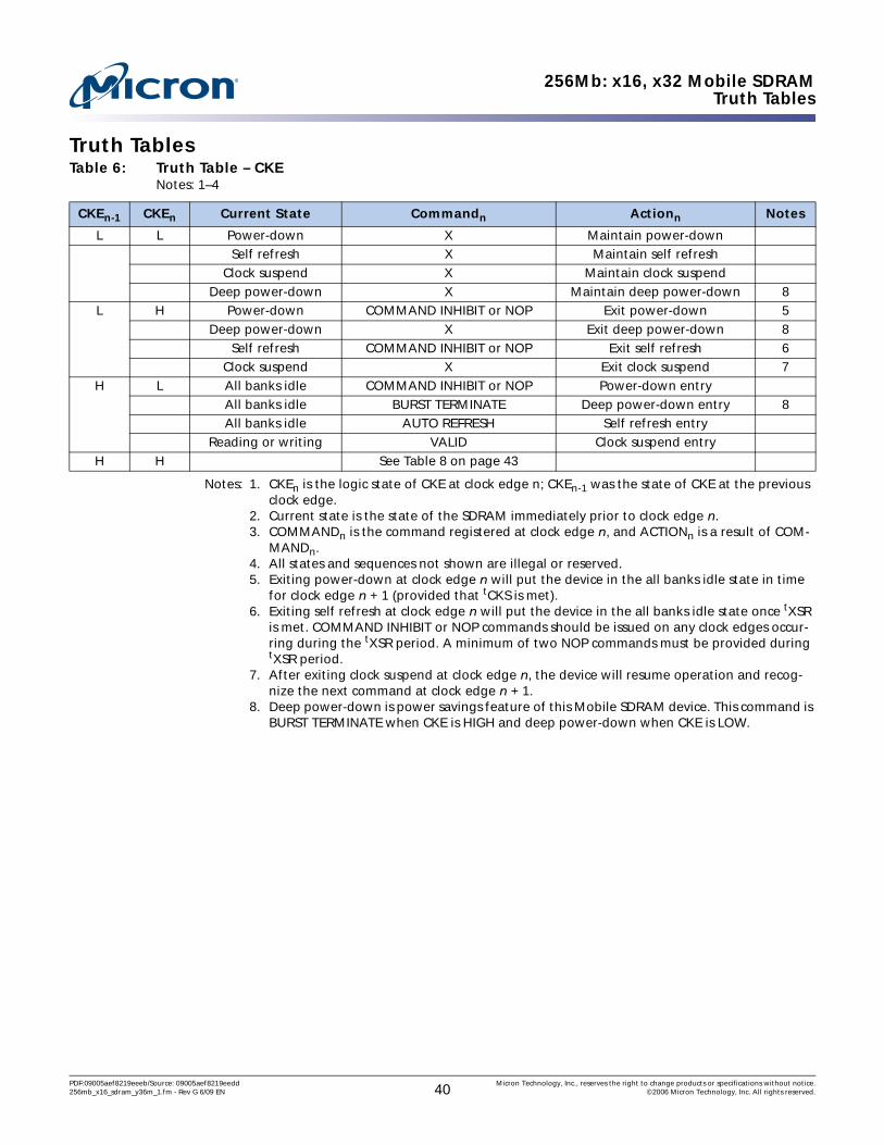
256Mb: x16, x32 Mobile SDRAMTruth Tables
Truth Tables
Notes: 1. CKEn is the logic state of CKE at clock edge n; CKEn-1 was the state of CKE at the previous clock edge.
2. Current state is the state of the SDRAM immediately prior to clock edge n.3. COMMANDn is the command registered at clock edge n, and ACTIONn is a result of COM-
MANDn.4. All states and sequences not shown are illegal or reserved.5. Exiting power-down at clock edge n will put the device in the all banks idle state in time
for clock edge n + 1 (provided that tCKS is met).6. Exiting self refresh at clock edge n will put the device in the all banks idle state once tXSR
is met. COMMAND INHIBIT or NOP commands should be issued on any clock edges occur-ring during the tXSR period. A minimum of two NOP commands must be provided during tXSR period.
7. After exiting clock suspend at clock edge n, the device will resume operation and recog-nize the next command at clock edge n + 1.
8. Deep power-down is power savings feature of this Mobile SDRAM device. This command is BURST TERMINATE when CKE is HIGH and deep power-down when CKE is LOW.
Table 6: Truth Table – CKENotes: 1–4
CKEn-1 CKEn Current State Commandn Actionn Notes
L L Power-down X Maintain power-downSelf refresh X Maintain self refresh
Clock suspend X Maintain clock suspendDeep power-down X Maintain deep power-down 8
L H Power-down COMMAND INHIBIT or NOP Exit power-down 5Deep power-down X Exit deep power-down 8
Self refresh COMMAND INHIBIT or NOP Exit self refresh 6Clock suspend X Exit clock suspend 7
H L All banks idle COMMAND INHIBIT or NOP Power-down entryAll banks idle BURST TERMINATE Deep power-down entry 8All banks idle AUTO REFRESH Self refresh entry
Reading or writing VALID Clock suspend entryH H See Table 8 on page 43
PDF:09005aef8219eeeb/Source: 09005aef8219eedd Micron Technology, Inc., reserves the right to change products or specifications without notice.256mb_x16_sdram_y36m_1.fm - Rev G 6/09 EN 40 ©2006 Micron Technology, Inc. All rights reserved.
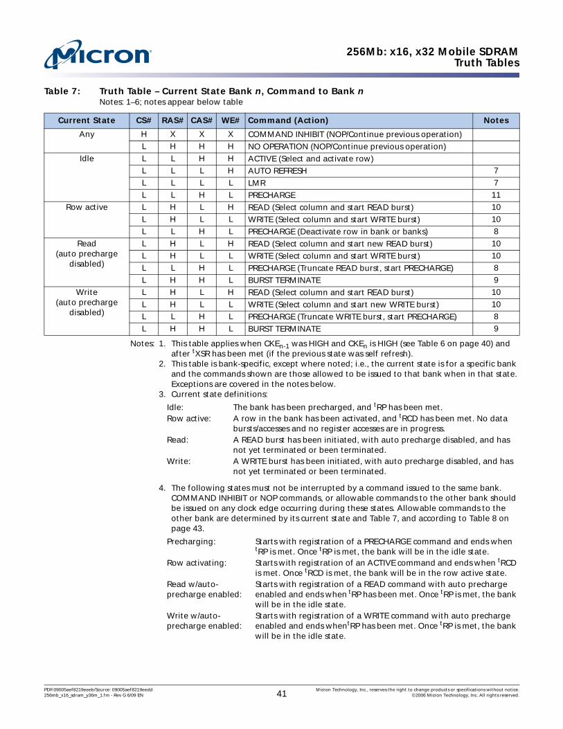
256Mb: x16, x32 Mobile SDRAMTruth Tables
Notes: 1. This table applies when CKEn-1 was HIGH and CKEn is HIGH (see Table 6 on page 40) and after tXSR has been met (if the previous state was self refresh).
2. This table is bank-specific, except where noted; i.e., the current state is for a specific bank and the commands shown are those allowed to be issued to that bank when in that state. Exceptions are covered in the notes below.
3. Current state definitions:
4. The following states must not be interrupted by a command issued to the same bank. COMMAND INHIBIT or NOP commands, or allowable commands to the other bank should be issued on any clock edge occurring during these states. Allowable commands to the other bank are determined by its current state and Table 7, and according to Table 8 on page 43.
Table 7: Truth Table – Current State Bank n, Command to Bank nNotes: 1–6; notes appear below table
Current State CS# RAS# CAS# WE# Command (Action) Notes
Any H X X X COMMAND INHIBIT (NOP/Continue previous operation)L H H H NO OPERATION (NOP/Continue previous operation)
Idle L L H H ACTIVE (Select and activate row)L L L H AUTO REFRESH 7L L L L LMR 7L L H L PRECHARGE 11
Row active L H L H READ (Select column and start READ burst) 10L H L L WRITE (Select column and start WRITE burst) 10L L H L PRECHARGE (Deactivate row in bank or banks) 8
Read (auto precharge
disabled)
L H L H READ (Select column and start new READ burst) 10L H L L WRITE (Select column and start WRITE burst) 10L L H L PRECHARGE (Truncate READ burst, start PRECHARGE) 8L H H L BURST TERMINATE 9
Write (auto precharge
disabled)
L H L H READ (Select column and start READ burst) 10L H L L WRITE (Select column and start new WRITE burst) 10L L H L PRECHARGE (Truncate WRITE burst, start PRECHARGE) 8L H H L BURST TERMINATE 9
Idle: The bank has been precharged, and tRP has been met.Row active: A row in the bank has been activated, and tRCD has been met. No data
bursts/accesses and no register accesses are in progress.Read: A READ burst has been initiated, with auto precharge disabled, and has
not yet terminated or been terminated.Write: A WRITE burst has been initiated, with auto precharge disabled, and has
not yet terminated or been terminated.
Precharging: Starts with registration of a PRECHARGE command and ends when tRP is met. Once tRP is met, the bank will be in the idle state.
Row activating: Starts with registration of an ACTIVE command and ends when tRCD is met. Once tRCD is met, the bank will be in the row active state.
Read w/auto-precharge enabled:
Starts with registration of a READ command with auto precharge enabled and ends when tRP has been met. Once tRP is met, the bank will be in the idle state.
Write w/auto-precharge enabled:
Starts with registration of a WRITE command with auto precharge enabled and ends whentRP has been met. Once tRP is met, the bank will be in the idle state.
PDF:09005aef8219eeeb/Source: 09005aef8219eedd Micron Technology, Inc., reserves the right to change products or specifications without notice.256mb_x16_sdram_y36m_1.fm - Rev G 6/09 EN 41 ©2006 Micron Technology, Inc. All rights reserved.

256Mb: x16, x32 Mobile SDRAMTruth Tables
5. The following states must not be interrupted by any executable command; DESELECT or NOP commands must be applied on each positive clock edge during these states.
6. All states and sequences not shown are illegal or reserved7. Not bank-specific; requires that all banks are idle.8. May or may not be bank-specific; if all banks are to be precharged, all must be in a valid
state for precharging.9. Not bank-specific; BURST TERMINATE affects the most recent READ or WRITE burst,
regardless of bank.10. READs or WRITEs listed in the Command (Action) column include READs or WRITEs with
auto precharge enabled and READs or WRITEs with auto precharge disabled.11. Does not affect the state of the bank and acts as a NOP to that bank.
Refreshing: Starts with registration of an AUTO REFRESH command and ends when tRFC is met. Once tRFC is met, the Mobile SDRAM will be in the all banks idle state.
Accessing mode register:
Starts with registration of an LMR command and ends when tMRD has been met. Once tMRD is met, the Mobile SDRAM will be in the all banks idle state.
Precharging all: Starts with registration of a PRECHARGE ALL command and ends when tRP is met. Once tRP is met, all banks will be in the idle state.
PDF:09005aef8219eeeb/Source: 09005aef8219eedd Micron Technology, Inc., reserves the right to change products or specifications without notice.256mb_x16_sdram_y36m_1.fm - Rev G 6/09 EN 42 ©2006 Micron Technology, Inc. All rights reserved.
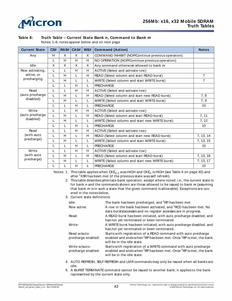
256Mb: x16, x32 Mobile SDRAMTruth Tables
Notes: 1. This table applies when CKEn-1 was HIGH and CKEn is HIGH (see Table 6 on page 40) and after tXSR has been met (if the previous state was self refresh).
2. This table describes alternate bank operation, except where noted; i.e., the current state is for bank n and the commands shown are those allowed to be issued to bank m (assuming that bank m is in such a state that the given command is allowable). Exceptions are cov-ered in the notes below.
3. Current state definitions:
4. AUTO REFRESH, SELF REFRESH and LMR commands may only be issued when all banks are idle.
5. A BURST TERMINATE command cannot be issued to another bank; it applies to the bank represented by the current state only.
Table 8: Truth Table – Current State Bank n, Command to Bank mNotes: 1–6; notes appear below and on next page
Current State CS# RAS# CAS# WE# Command (Action) Notes
Any H X X X COMMAND INHIBIT (NOP/Continue previous operation)L H H H NO OPERATION (NOP/Continue previous operation)
Idle X X X X Any command otherwise allowed to bank mRow activating,
active, orprecharging
L L H H ACTIVE (Select and activate row)L H L H READ (Select column and start READ burst) 7L H L L WRITE (Select column and start WRITE burst) 7L L H L PRECHARGE
Read(auto precharge
disabled)
L L H H ACTIVE (Select and activate row)L H L H READ (Select column and start new READ burst) 7, 8L H L L WRITE (Select column and start WRITE burst) 7, 9L L H L PRECHARGE 10
Write(auto precharge
disabled)
L L H H ACTIVE (Select and activate row)L H L H READ (Select column and start READ burst) 7, 11L H L L WRITE (Select column and start new WRITE burst) 7, 12L L H L PRECHARGE 10
Read(with autoprecharge)
L L H H ACTIVE (Select and activate row)L H L H READ (Select column and start new READ burst) 7, 13, 14L H L L WRITE (Select column and start WRITE burst) 7, 13, 15L L H L PRECHARGE 10
Write(with autoprecharge)
L L H H ACTIVE (Select and activate row)L H L H READ (Select column and start READ burst) 7, 13, 16L H L L WRITE (Select column and start new WRITE burst) 7, 13, 17L L H L PRECHARGE 10
Idle: The bank has been precharged, and tRP has been met.Row active: A row in the bank has been activated, and tRCD has been met. No
data bursts/accesses and no register accesses are in progress.Read: A READ burst has been initiated, with auto precharge disabled, and
has not yet terminated or been terminated.Write: A WRITE burst has been initiated, with auto precharge disabled, and
has not yet terminated or been terminated.Read w/auto-precharge enabled:
Starts with registration of a READ command with auto precharge enabled and ends when tRP has been met. Once tRP is met, the bank will be in the idle state.
Write w/auto-precharge enabled:
Starts with registration of a WRITE command with auto precharge enabled and ends when tRP has been met. Once tRP is met, the bank will be in the idle state.
PDF:09005aef8219eeeb/Source: 09005aef8219eedd Micron Technology, Inc., reserves the right to change products or specifications without notice.256mb_x16_sdram_y36m_1.fm - Rev G 6/09 EN 43 ©2006 Micron Technology, Inc. All rights reserved.

256Mb: x16, x32 Mobile SDRAMTruth Tables
6. All states and sequences not shown are illegal or reserved.7. READs or WRITEs to bank m listed in the Command (Action) column include READs or
WRITEs with auto precharge enabled and READs or WRITEs with auto precharge disabled.8. For a READ without auto precharge interrupted by a READ (with or without auto pre-
charge), the READ to bank m will interrupt the READ on bank n, CL later (see Figure 11 on page 24).
9. For a READ without auto precharge interrupted by a WRITE (with or without auto pre-charge), the WRITE to bank m will interrupt the READ on bank n when registered (see Figure 12 on page 25 and Figure 13 on page 26). DQM should be used one clock prior to the WRITE command to prevent bus contention.
10. Burst in bank n continues as initiated.11. For a WRITE without auto precharge interrupted by a READ (with or without auto pre-
charge), the READ to bank m will interrupt the WRITE on bank n when registered (see Figure 20 on page 31), with the data-out appearing CL later. The last valid WRITE to bank n will be data-in registered one clock prior to the READ to bank m.
12. For a WRITE without auto precharge interrupted by a WRITE (with or without auto pre-charge), the WRITE to bank will interrupt the WRITE on bank n when registered (see Figure 18 on page 30). The last valid WRITE to bank n will be data-in registered one clock prior to the READ to bank m.
13. Concurrent auto precharge: Bank n will initiate the auto precharge command when its burst has been interrupted by bank m burst.
14. For a READ with auto precharge interrupted by a READ (with or without auto precharge), the READ to bank m will interrupt the READ on bank n, CL later. The PRECHARGE to bank n will begin when the READ to bank m is registered.
15. For a READ with auto precharge interrupted by a WRITE (with or without auto precharge), the WRITE to bank m will interrupt the READ on bank n when registered. DQM should be used two clocks prior to the WRITE command to prevent bus contention. The PRECHARGE to bank n will begin when the WRITE to bank m is registered.
16. For a WRITE with auto precharge interrupted by a READ (with or without auto precharge), the READ to bank m will interrupt the WRITE on bank n when registered, with the data-out appearing CL later. The PRECHARGE to bank n will begin after tWR is met, where tWR begins when the READ to bank m is registered. The last valid WRITE bank n will be data-in registered one clock prior to the READ to bank m.
17. For a WRITE with auto precharge interrupted by a WRITE (with or without auto pre-charge), the WRITE to bank m interrupt the WRITE on bank n when registered. The PRE-CHARGE to bank n will begin after tWR is met, where tWR begins when the WRITE to bank m is registered. The last valid WRITE to bank n will be data registered one clock to the WRITE to bank m.
PDF:09005aef8219eeeb/Source: 09005aef8219eedd Micron Technology, Inc., reserves the right to change products or specifications without notice.256mb_x16_sdram_y36m_1.fm - Rev G 6/09 EN 44 ©2006 Micron Technology, Inc. All rights reserved.

256Mb: x16, x32 Mobile SDRAMElectrical Specifications
Electrical Specifications
Absolute Maximum Ratings
Stresses greater than those listed in Table 9 may cause permanent damage to the device. This is a stress rating only, and functional operation of the device at these or any other conditions above those indicated in the operational sections of this specification is not implied. Exposure to absolute maximum rating conditions for extended periods may affect reliability.
Table 9: Absolute Maximum Ratings
Voltage/Temperature Min Max Units
Voltage on VDD/VDDQ supply relative to VSS (1.8V) –0.3 +2.7 V
Voltage on inputs, NC or I/O balls relative to VSS (1.8V) –0.3 +2.7
Storage temperature plastic –55 +150
Table 10: DC Electrical Characteristics and Operating Conditions Notes: 1, 5, 6; notes appear on page 52 and 53; VDD/VDDQ = 1.7–1.95V
Parameter/Condition Symbol Min Max Units Notes
Supply voltage VDD 1.7 1.95 V
I/O supply voltage VDDQ 1.7 1.95 V
Input high voltage: Logic 1; All inputs VIH 0.8 × VDDQ VDDQ + 0.3 V 22
Input low voltage: Logic 0; All inputs VIL –0.3 +0.3 V 22
Output high voltage: All inputs: IOUT = –4mA VOH 0.9 × VDDQ – V
Output low voltage: All inputs: IOUT = 4mA VOL – 0.2 V
Input leakage current:Any input 0V ≤ VIN ≤ VDD (All other balls not under test = 0V)
II –1.0 1.0 µA
Output leakage current: DQ are disabled; 0V ≤ VOUT ≤ VDDQ IOZ -1.5 1.5 µA
Operating temperatureTA (commercial)TA (industrial)
+70+85
°C
PDF:09005aef8219eeeb/Source: 09005aef8219eedd Micron Technology, Inc., reserves the right to change products or specifications without notice.256mb_x16_sdram_y36m_1.fm - Rev G 6/09 EN 45 ©2006 Micron Technology, Inc. All rights reserved.
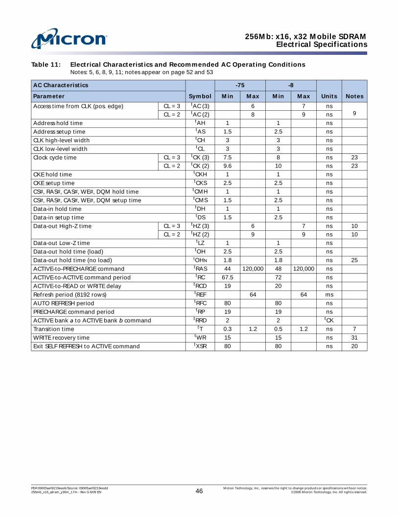
256Mb: x16, x32 Mobile SDRAMElectrical Specifications
Table 11: Electrical Characteristics and Recommended AC Operating ConditionsNotes: 5, 6, 8, 9, 11; notes appear on page 52 and 53
AC Characteristics
Symbol
-75 -8
Units NotesParameter Min Max Min Max
Access time from CLK (pos. edge) CL = 3 tAC (3) 6 7 ns9CL = 2 tAC (2) 8 9 ns
Address hold time tAH 1 1 ns
Address setup time tAS 1.5 2.5 ns
CLK high-level width tCH 3 3 ns
CLK low-level width tCL 3 3 ns
Clock cycle time CL = 3 tCK (3) 7.5 8 ns 23CL = 2 tCK (2) 9.6 10 ns 23
CKE hold time tCKH 1 1 ns
CKE setup time tCKS 2.5 2.5 ns
CS#, RAS#, CAS#, WE#, DQM hold time tCMH 1 1 ns
CS#, RAS#, CAS#, WE#, DQM setup time tCMS 1.5 2.5 ns
Data-in hold time tDH 1 1 ns
Data-in setup time tDS 1.5 2.5 ns
Data-out High-Z time CL = 3 tHZ (3) 6 7 ns 10CL = 2 tHZ (2) 9 9 ns 10
Data-out Low-Z time tLZ 1 1 ns
Data-out hold time (load) tOH 2.5 2.5 ns
Data-out hold time (no load) tOHN 1.8 1.8 ns 25
ACTIVE-to-PRECHARGE command tRAS 44 120,000 48 120,000 ns
ACTIVE-to-ACTIVE command period tRC 67.5 72 ns
ACTIVE-to-READ or WRITE delay tRCD 19 20 ns
Refresh period (8192 rows) tREF 64 64 ms
AUTO REFRESH period tRFC 80 80 ns
PRECHARGE command period tRP 19 19 ns
ACTIVE bank a to ACTIVE bank b command tRRD 2 2 tCK
Transition time tT 0.3 1.2 0.5 1.2 ns 7
WRITE recovery time tWR 15 15 ns 31
Exit SELF REFRESH to ACTIVE command tXSR 80 80 ns 20
PDF:09005aef8219eeeb/Source: 09005aef8219eedd Micron Technology, Inc., reserves the right to change products or specifications without notice.256mb_x16_sdram_y36m_1.fm - Rev G 6/09 EN 46 ©2006 Micron Technology, Inc. All rights reserved.

256Mb: x16, x32 Mobile SDRAMElectrical Specifications
Table 12: AC Functional CharacteristicsNotes: 5, 6, 8, 9,11 notes appear on page 52 and 53
Parameter Symbol -75 -8 Units Notes
READ/WRITE command to READ/WRITE command tCCD 1 1 tCK 17
CKE to clock disable or power-down entry mode tCKED 1 1 tCK 14
CKE to clock enable or power-down exit setup mode tPED 1 1 tCK 14
DQM to input data delay tDQD 0 0 tCK 17
DQM to data mask during WRITEs tDQM 0 0 tCK 17
DQM to data High-Z during READs tDQZ 2 2 tCK 17
WRITE command to input data delay tDWD 0 0 tCK 17
Data-in to ACTIVE command tDAL 5 5 tCK 15, 21
Data-in to PRECHARGE command tDPL 2 2 tCK 16, 21
Last data-in to burst STOP command tBDL 1 1 tCK 17
Last data-in to new READ/WRITE command tCDL 1 1 tCK 17
Last data-in to PRECHARGE command tRDL 2 2 tCK 16, 21
LMR command to ACTIVE or REFRESH command tMRD 2 2 tCK 25
Data-out High-Z from PRECHARGE command CL = 3 tROH(3) 3 3 tCK 17CL = 2 tROH(2) 2 2 tCK 17
PDF:09005aef8219eeeb/Source: 09005aef8219eedd Micron Technology, Inc., reserves the right to change products or specifications without notice.256mb_x16_sdram_y36m_1.fm - Rev G 6/09 EN 47 ©2006 Micron Technology, Inc. All rights reserved.

256Mb: x16, x32 Mobile SDRAMElectrical Specifications
Table 13: IDD Specifications and Conditions (x16)Notes: 1, 5, 6, 11, 13; notes appear on page 52 and 53; VDD/VDDQ = 1.7–1.95V
Parameter/Condition Symbol
Max
Units Notes-75 -8
Operating current: Active mode; BL = 1; READ or WRITE; tRC = tRC (MIN)
IDD1 65 60 mA 1, 18, 19
Standby current:Power-down mode; All banks idle; CKE = LOW
IDD2Pstandard
300 300 µA 1, 18, 19
IDD2Plow-power
220 220 µA 1, 18, 19
Precharge nonpower-down standby current with clock stopped: All banks idle; CKE is LOW, CS is HIGH; CK = LOW, CK# = HIGH; Address and control inputs are switching; Data bus inputs are stable
IDD2PSstandard
300 300 µA 30
IDD2PSlow-power
220 220 µA 30
Standby current: Non-power-down mode; All banks idle; CKE = HIGH
IDD2N 20 20 mA
Precharge nonpower-down standby current with clock stopped: All banks idle; CKE is LOW, CS is HIGH; CK = LOW, CK# = HIGH; Address and control inputs are switching; Data bus inputs are stable
IDD2NS 5 5 mA
Standby current: Active mode; CKE = LOW; CS# = HIGH; All banks active; No accesses in progress
IDD3P 5 5 mA 1, 12, 19
Precharge nonpower-down standby current with clock stopped: All banks idle; CKE is LOW, CS is HIGH; CK = LOW, CK# = HIGH; Address and control inputs are switching; Data bus inputs are stable
IDD3PS 3 3 mA
Standby current: Active mode; CKE = HIGH; CS# = HIGH; All banks active after tRCD met; No accesses in progress
IDD3N 25 25 mA 1, 12, 19
Precharge nonpower-down standby current with clock stopped: All banks idle; CKE is LOW, CS is HIGH; CK = LOW, CK# = HIGH; Address and control inputs are switching; Data bus inputs are stable
IDD3NS 10 10 mA
Operating current: Burst mode; READ or WRITE; All banks active, half DQs toggling every cycle
IDD4 90 85 mA 1, 18, 19
Auto refresh current:CKE = HIGH; CS# = HIGH
tRFC = tRFC (MIN) IDD5 100 95 mA 1, 12, 18 19,
26tRFC = 7.8125µs IDD6 5 5 mA
Deep power-down IZZ 10 10 µA 29, 30
PDF:09005aef8219eeeb/Source: 09005aef8219eedd Micron Technology, Inc., reserves the right to change products or specifications without notice.256mb_x16_sdram_y36m_1.fm - Rev G 6/09 EN 48 ©2006 Micron Technology, Inc. All rights reserved.
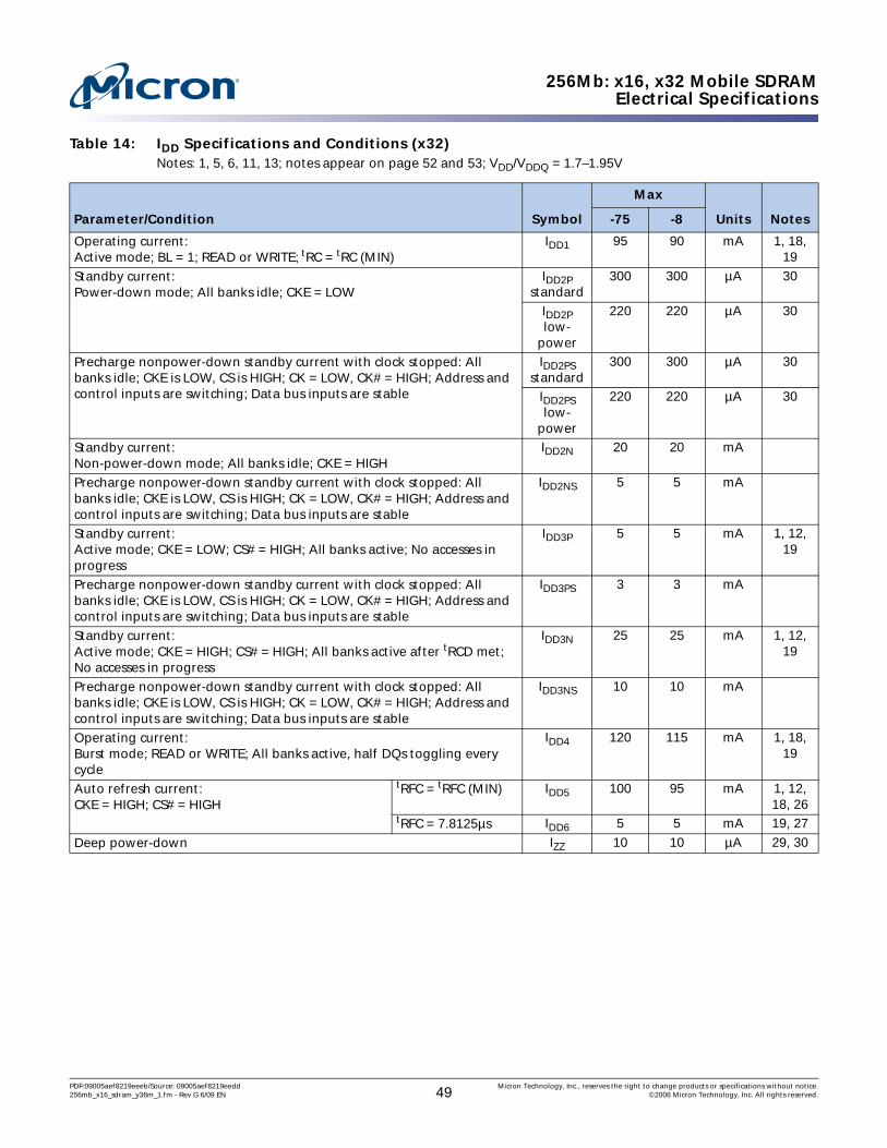
256Mb: x16, x32 Mobile SDRAMElectrical Specifications
Table 14: IDD Specifications and Conditions (x32)Notes: 1, 5, 6, 11, 13; notes appear on page 52 and 53; VDD/VDDQ = 1.7–1.95V
Parameter/Condition Symbol
Max
Units Notes-75 -8
Operating current: Active mode; BL = 1; READ or WRITE; tRC = tRC (MIN)
IDD1 95 90 mA 1, 18, 19
Standby current:Power-down mode; All banks idle; CKE = LOW
IDD2Pstandard
300 300 µA 30
IDD2Plow-
power
220 220 µA 30
Precharge nonpower-down standby current with clock stopped: All banks idle; CKE is LOW, CS is HIGH; CK = LOW, CK# = HIGH; Address and control inputs are switching; Data bus inputs are stable
IDD2PSstandard
300 300 µA 30
IDD2PSlow-
power
220 220 µA 30
Standby current: Non-power-down mode; All banks idle; CKE = HIGH
IDD2N 20 20 mA
Precharge nonpower-down standby current with clock stopped: All banks idle; CKE is LOW, CS is HIGH; CK = LOW, CK# = HIGH; Address and control inputs are switching; Data bus inputs are stable
IDD2NS 5 5 mA
Standby current: Active mode; CKE = LOW; CS# = HIGH; All banks active; No accesses in progress
IDD3P 5 5 mA 1, 12, 19
Precharge nonpower-down standby current with clock stopped: All banks idle; CKE is LOW, CS is HIGH; CK = LOW, CK# = HIGH; Address and control inputs are switching; Data bus inputs are stable
IDD3PS 3 3 mA
Standby current: Active mode; CKE = HIGH; CS# = HIGH; All banks active after tRCD met; No accesses in progress
IDD3N 25 25 mA 1, 12, 19
Precharge nonpower-down standby current with clock stopped: All banks idle; CKE is LOW, CS is HIGH; CK = LOW, CK# = HIGH; Address and control inputs are switching; Data bus inputs are stable
IDD3NS 10 10 mA
Operating current: Burst mode; READ or WRITE; All banks active, half DQs toggling every cycle
IDD4 120 115 mA 1, 18, 19
Auto refresh current:CKE = HIGH; CS# = HIGH
tRFC = tRFC (MIN) IDD5 100 95 mA 1, 12, 18, 26
tRFC = 7.8125µs IDD6 5 5 mA 19, 27
Deep power-down IZZ 10 10 µA 29, 30
PDF:09005aef8219eeeb/Source: 09005aef8219eedd Micron Technology, Inc., reserves the right to change products or specifications without notice.256mb_x16_sdram_y36m_1.fm - Rev G 6/09 EN 49 ©2006 Micron Technology, Inc. All rights reserved.
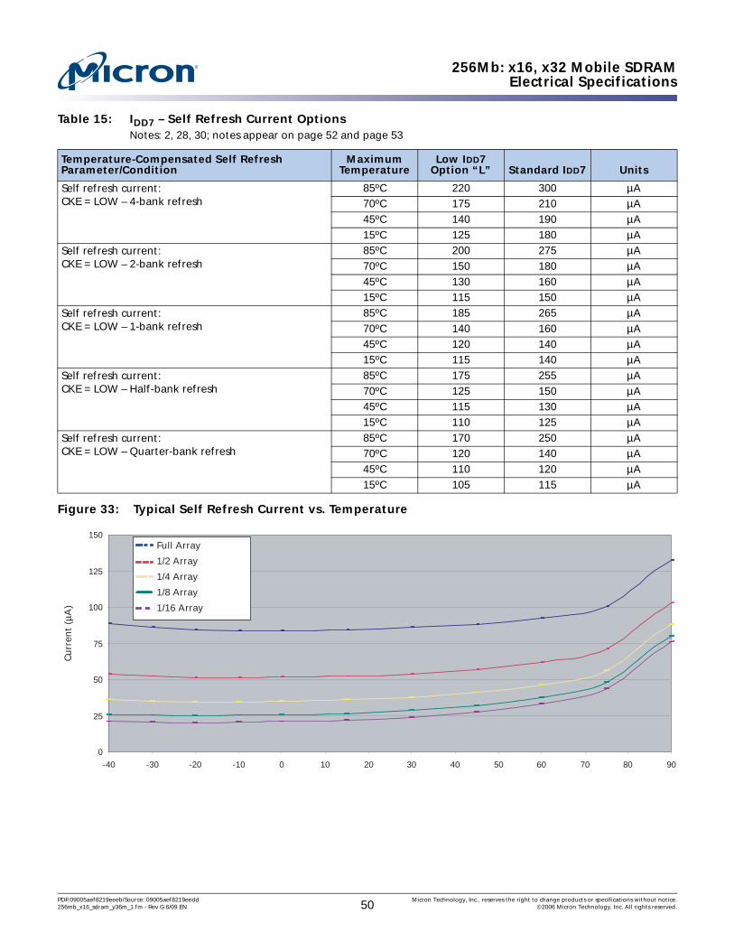
256Mb: x16, x32 Mobile SDRAMElectrical Specifications
Figure 33: Typical Self Refresh Current vs. Temperature
Table 15: IDD7 – Self Refresh Current OptionsNotes: 2, 28, 30; notes appear on page 52 and page 53
Temperature-Compensated Self Refresh Parameter/Condition
Maximum Temperature
Low IDD7 Option “L” Standard IDD7 Units
Self refresh current:CKE = LOW – 4-bank refresh
85ºC 220 300 µA70ºC 175 210 µA45ºC 140 190 µA15ºC 125 180 µA
Self refresh current:CKE = LOW – 2-bank refresh
85ºC 200 275 µA70ºC 150 180 µA45ºC 130 160 µA15ºC 115 150 µA
Self refresh current:CKE = LOW – 1-bank refresh
85ºC 185 265 µA70ºC 140 160 µA45ºC 120 140 µA15ºC 115 140 µA
Self refresh current:CKE = LOW – Half-bank refresh
85ºC 175 255 µA70ºC 125 150 µA45ºC 115 130 µA15ºC 110 125 µA
Self refresh current:CKE = LOW – Quarter-bank refresh
85ºC 170 250 µA70ºC 120 140 µA45ºC 110 120 µA15ºC 105 115 µA
Temperature (°C)
Cu
rren
t (µ
A)
0
25
50
75
100
125
150
-40 -30 -20 -10 0 10 20 30 40 50 60 70 80 90
Full Array
1/2 Array
1/4 Array
1/8 Array
1/16 Array
PDF:09005aef8219eeeb/Source: 09005aef8219eedd Micron Technology, Inc., reserves the right to change products or specifications without notice.256mb_x16_sdram_y36m_1.fm - Rev G 6/09 EN 50 ©2006 Micron Technology, Inc. All rights reserved.
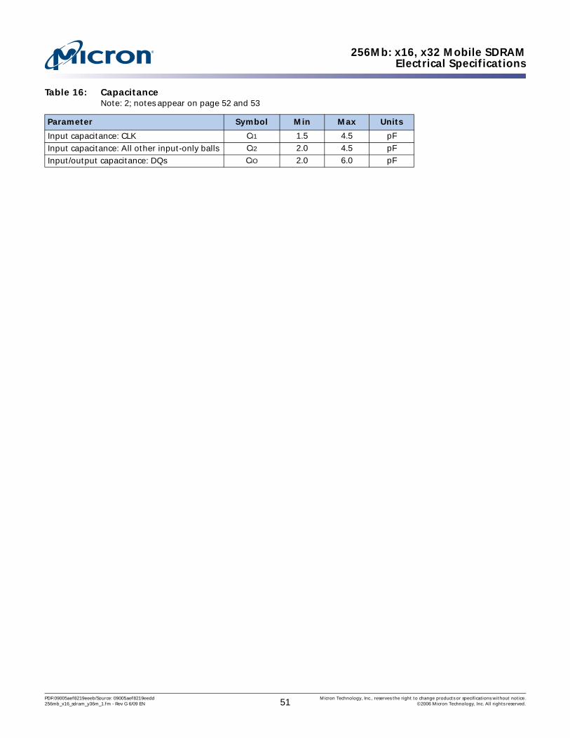
256Mb: x16, x32 Mobile SDRAMElectrical Specifications
Table 16: CapacitanceNote: 2; notes appear on page 52 and 53
Parameter Symbol Min Max Units
Input capacitance: CLK CI1 1.5 4.5 pF
Input capacitance: All other input-only balls CI2 2.0 4.5 pF
Input/output capacitance: DQs CIO 2.0 6.0 pF
PDF:09005aef8219eeeb/Source: 09005aef8219eedd Micron Technology, Inc., reserves the right to change products or specifications without notice.256mb_x16_sdram_y36m_1.fm - Rev G 6/09 EN 51 ©2006 Micron Technology, Inc. All rights reserved.
256Mb: x16, x32 Mobile SDRAMNotes
Notes1. All voltages referenced to VSS.2. This parameter is sampled. VDD, VDDQ = +1.8V; TA = 25°C; ball under test biased at
0.9V; f = 1 MHz. 3. IDD is dependent on output loading and cycle rates. Specified values are obtained
with minimum cycle time and the outputs open.4. Enables on-chip refresh and address counters. 5. The minimum specifications are used only to indicate cycle time at which proper
operation over the full temperature range (–40°C ≤ TA ≤ +85°C for TA on IT parts) isensured.
6. An initial pause of 100µs is required after power-up, followed by two AUTO REFRESHcommands, before proper device operation is ensured. (VDD and VDDQ must be pow-ered up simultaneously. VSS and VSSQ must be at same potential.) The two AUTOREFRESH command wake-ups should be repeated any time the tREF refresh require-ment is exceeded.
7. AC characteristics assume tT = 1ns.8. In addition to meeting the transition rate specification, the clock and CKE must tran-
sit between VIH and VIL (or between VIL and VIH) in a monotonic manner. 9. Outputs measured for 1.8V at 0.9V with equivalent load:
Test loads with full DQ driver strength. Performance will vary with actual system DQbus capacitive loading, termination, and programmed drive strength.
10. tHZ defines the time at which the output achieves the open circuit condition; it is nota reference to VOH or VOL. The last valid data element will meet tOH before goingHigh-Z.
11. AC timing and IDD tests have VIL and VIH, with timing referenced to VIH/2 = crossoverpoint. If the input transition time is longer than tT (MAX), then the timing is refer-enced at VIL,max and VIH,min and no longer at the VIH/2 crossover point.
12. Other input signals are allowed to transition no more than once every two clocks andare otherwise at valid VIH or VIL levels.
13. IDD specifications are tested after the device is properly initialized.14. Timing actually specified by tCKS; clock(s) specified as a reference only at minimum
cycle rate.15. Timing actually specified by tWR plus tRP; clock(s) specified as a reference only at
minimum cycle rate. 16. Timing actually specified by tWR.17. Required clocks are specified by JEDEC functionality and are not dependent on any
timing parameter. 18. The IDD current will increase or decrease proportionally according to the amount of
frequency alteration for the test condition.19. Address transitions average one transition every two clocks.20. CLK must be toggled a minimum of two times during this period.21. Based on tCK = 7.5ns for -75,tCK = 8ns for -8, at CL = 3.
Q
20pF
PDF:09005aef8219eeeb/Source: 09005aef8219eedd Micron Technology, Inc., reserves the right to change products or specifications without notice.256mb_x16_sdram_y36m_1.fm - Rev G 6/09 EN 52 ©2006 Micron Technology, Inc. All rights reserved.
256Mb: x16, x32 Mobile SDRAMNotes
22. VIH overshoot: VIH,max = VDDQ + 2V for a pulse width ≤ 3ns, and the pulse width can-not be greater than one third of the cycle rate. VIL undershoot: VIL,min = –2V for a pulsewidth ≤ 3ns.
23. The clock frequency can only be changed during clock stop, power-down, or while ina self-refresh mode.
24. Auto precharge mode only. The precharge timing budget (tRP) begins at 7ns for -8after the first clock delay, after the last WRITE is executed. May not exceed limit set forprecharge mode.The clock frequency can only be changed during
25. Parameter guaranteed by design. 26. CKE is HIGH during refresh command period tRFC (MIN), else CKE is LOW. 27. The IDD6 limit is actually a nominal value and does not result in a fail value.28. Values for IDD7 for 70°C, 45°C, 15°C, and IDD7 1/2-bank and 1/4-bank are sampled
only. Values for IDD7 4-bank, 2-bank, and 1-bank for 85°C are 100% tested.29. Deep power-down current is a nominal value at 25°C. This parameter is not tested.30. Test conditions include 500ms delay prior to measurement.31. Auto precharge mode only. The precharge timing budget (tRP) begins at 7.5ns for -75
and 7ns for -8 after the first clock delay, after the last WRITE is executed. For auto pre-charge mode, at least one clock cycle is required during tWR.
PDF:09005aef8219eeeb/Source: 09005aef8219eedd Micron Technology, Inc., reserves the right to change products or specifications without notice.256mb_x16_sdram_y36m_1.fm - Rev G 6/09 EN 53 ©2006 Micron Technology, Inc. All rights reserved.
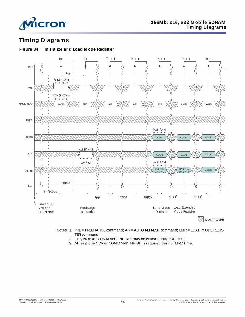
256Mb: x16, x32 Mobile SDRAMTiming Diagrams
Timing Diagrams
Figure 34: Initialize and Load Mode Register
Notes: 1. PRE = PRECHARGE command; AR = AUTO REFRESH command; LMR = LOAD MODE REGIS-TER command.
2. Only NOPs or COMMAND INHIBITs may be issued during tRFC time.3. At least one NOP or COMMAND INHIBIT is required during tMRD time.
CKE
BA[1:0]
Load Extended Mode Register
Load Mode Register
tCKS
Power-up: VDD and CLK stable
T = 100µs
tCKH
( ) ( )
( ) ( )
( ) ( )
( ) ( )
( ) ( )
( ) ( )
( ) ( )
( ) ( )
( ) ( )
( ) ( )
DQM
( ) ( )
( ) ( )
DQ High-Z
ADDR VALID
A10 VALID
CLK
tCK
COMMAND1 AR NOP LMR AR LMR VALID
tCMS tCMH
tAS tAH
BA0 = L, BA1 = L
( ) ( )
( ) ( )
CODE CODE
t AS t AH
CODE CODE
( ) ( )
( ) ( )
PRE
ALL BANKS
t AS t AH
( ) ( )
( ) ( )
T0 T1
DON’T CARE
( ) ( )
( ) ( )
( ) ( )
( ) ( )
( ) ( )
( ) ( )
( ) ( )
( ) ( )
( ) ( )
( ) ( )
( ) ( )
( ) ( )
( ) ( )
( ) ( )
( ) ( )
( ) ( )
( ) ( )
( ) ( )
( ) ( )
( ) ( )
( ) ( )
( ) ( )
( ) ( )
( ) ( )
( ) ( )
( ) ( )
( ) ( )
tRP tMRD3 tMRD3 tRFC2 tRFC2
( ) ( )
( ) ( )
( ) ( )
( ) ( )
( ) ( )
( ) ( )
( ) ( )
( ) ( )
VALID
( ) ( )
( ) ( )
( ) ( )
( ) ( )
( ) ( )
( ) ( )
( ) ( )
( ) ( )
( ) ( )
( ) ( )
BA0 = L, BA1 = L
BA0 = L, BA1 = H
( ) ( )
( ) ( )
( ) ( )
( ) ( )
( ) ( )
( ) ( )
( ) ( )
( ) ( )
( ) ( )
( ) ( )
( ) ( )
( ) ( )
( ) ( )
( ) ( )
( ) ( )
( ) ( )
( ) ( )
( ) ( )
( ) ( )
( ) ( )
( ) ( )
( ) ( )
( ) ( )
( ) ( )
Precharge all banks
( ) ( )
( ) ( )
Tn + 1 To + 1 Tp + 1 Tq + 1 Tr + 1
( ) ( )
( ) ( )
( ) ( )
( ) ( )
( ) ( )
( ) ( )
( ) ( )
( ) ( )
( ) ( )
( ) ( )
( ) ( )
( ) ( )
( ) ( )
( ) ( )
( ) ( )
( ) ( )
( ) ( )
( ) ( )
PDF:09005aef8219eeeb/Source: 09005aef8219eedd Micron Technology, Inc., reserves the right to change products or specifications without notice.256mb_x16_sdram_y36m_1.fm - Rev G 6/09 EN 54 ©2006 Micron Technology, Inc. All rights reserved.

256Mb: x16, x32 Mobile SDRAMTiming Diagrams
Figure 35: Power-Down Mode
Notes: 1. Violating refresh requirements during power-down may result in a loss of data.See Table 11 on page 46.
t CH
t CL t CK
Two clock cycles
CKE
CLK
DQ
All banks idle, enter power-down mode
Precharge all active banks
Input buffers gated off while in
power-down mode
Exit power-down mode
( ) ( )
()()
DON’T CARE
t CKS t CKS
COMMAND
t CMH t CMS
PRECHARGE NOP NOP ACTIVE NOP
All banks idle
BA[1:0] BANK BANK(S)
High-Z
t AH t AS
t CKH t CKS
DQM
()()
()()
ADDR ROW
ALL BANKS
SINGLE BANK
A10 ROW
T0 T1 T2 Tn + 1 Tn + 2
()()
()()
()()
()()
()()
()()
()()
()()
()()
()()
PDF:09005aef8219eeeb/Source: 09005aef8219eedd Micron Technology, Inc., reserves the right to change products or specifications without notice.256mb_x16_sdram_y36m_1.fm - Rev G 6/09 EN 55 ©2006 Micron Technology, Inc. All rights reserved.
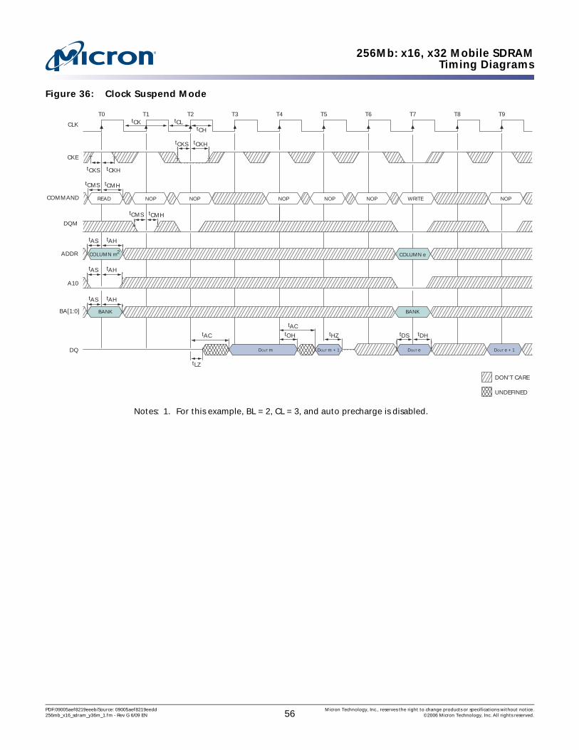
256Mb: x16, x32 Mobile SDRAMTiming Diagrams
Figure 36: Clock Suspend Mode
Notes: 1. For this example, BL = 2, CL = 3, and auto precharge is disabled.
t CH
t CL t CK
t AC
t LZ
DQM
CLK
DQ
A10
t OH
DOUT m
t AH t AS
t AH t AS
t AH t AS
BANK
t DH
DOUT e
t AC t HZ
DOUT m + 1
COMMAND
t CMH t CMS
NOP NOP NOP NOP NOP READ WRITE
DON’T CARE
UNDEFINED
CKE
t CKS t CKH
BANK
COLUMN m
t DS
DOUT e + 1
NOP
t CKH t CKS
t CMH t CMS
2 COLUMN e
T0 T1 T2 T3 T4 T5 T6 T7 T8 T9
BA[1:0]
ADDR
PDF:09005aef8219eeeb/Source: 09005aef8219eedd Micron Technology, Inc., reserves the right to change products or specifications without notice.256mb_x16_sdram_y36m_1.fm - Rev G 6/09 EN 56 ©2006 Micron Technology, Inc. All rights reserved.
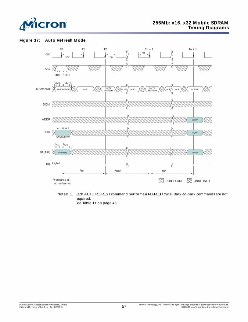
256Mb: x16, x32 Mobile SDRAMTiming Diagrams
Figure 37: Auto Refresh Mode
Notes: 1. Each AUTO REFRESH command performs a REFRESH cycle. Back-to-back commands are not required.See Table 11 on page 46.
UNDEFINED DON’T CARE
t CH
t CL t CK
CKE
CLK
DQ
t RFC
( ) ( )
( ) ( )
( ) ( )
t RP
( ) ( )
( ) ( )
( ) ( )
( ) ( )
COMMAND
t CMH t CMS
NOP NOP
( ) ( )
( ) ( )
BANK
ACTIVE AUTO
REFRESH
( ) ( )
( ) ( )
NOP NOP PRECHARGE
Precharge all active banks
AUTO REFRESH
t RFC
High-Z
BANK(S)
( ) ( )
( ) ( )
( ) ( )
( ) ( )
t AH t AS
t CKH t CKS
( ) ( )
NOP
( ) ( )
( ) ( )
( ) ( )
( ) ( )
ROW
( ) ( )
( ) ( )
ALL BANKS
SINGLE BANK
A10 ROW
( ) ( )
( ) ( )
( ) ( )
( ) ( )
( ) ( )
( ) ( )
( ) ( )
( ) ( )
T0 T1 T2 Tn + 1 To + 1
BA[1:0]
ADDR
DQM
PDF:09005aef8219eeeb/Source: 09005aef8219eedd Micron Technology, Inc., reserves the right to change products or specifications without notice.256mb_x16_sdram_y36m_1.fm - Rev G 6/09 EN 57 ©2006 Micron Technology, Inc. All rights reserved.

256Mb: x16, x32 Mobile SDRAMTiming Diagrams
Figure 38: Self Refresh Mode
t CH
t CL t CK
t RP
CKE
CLK
DQ
Enter self refresh mode Precharge all active banks
t XSR
CLK stable prior to exiting self refresh mode
Exit self refresh mode (Restart refresh time base)
( ) ( )
DON’T CARE
COMMAND
t CMH t CMS
AUTO REFRESH PRECHARGE NOP NOP
BANK(S)
High-Z
t CKS
AH AS
AUTO REFRESH
> t RAS
t CKH t CKS
t t
ALL BANKS
SINGLE BANK
A10
T0 T1 T2 Tn + 1 To + 1 To + 2
BA[1:0]
DQM
ADDR
( ) ( )
( ) ( )
( ) ( )
( ) ( )
( ) ( )
( ) ( )
( ) ( )
( ) ( )
( ) ( )
( ) ( )
( ) ( )
( ) ( )
( ) ( )
( ) ( )
( ) ( )
( ) ( )
( ) ( )
( ) ( )
( ) ( )
( ) ( )
( ) ( )
( ) ( )
( ) ( )
( ) ( )
( ) ( )
( ) ( )
( ) ( )
( ) ( )
PDF:09005aef8219eeeb/Source: 09005aef8219eedd Micron Technology, Inc., reserves the right to change products or specifications without notice.256mb_x16_sdram_y36m_1.fm - Rev G 6/09 EN 58 ©2006 Micron Technology, Inc. All rights reserved.

256Mb: x16, x32 Mobile SDRAMTiming Diagrams
Figure 39: READ – without Auto Precharge
Notes: 1. For this example, BL = 4, CL = 2, and the READ burst is followed by a manual PRECHARGE.
ALL BANKS
t CH
t CL t CK
t AC
t LZ
t RP
t RAS
t RCD CL
t RC
CKE
CLK
DQ
A10
t OH
DOUT m
t CMH t CMS
t AH t AS
t AH t AS
t AH t AS
ROW
ROW
BANK BANK(S) BANK
ROW
ROW
BANK
t HZ
t OH
DOUT m + 3
t AC t OH
t AC t OH
t AC
DOUT m + 2 DOUT m + 1
COMMAND
t CMH t CMS
PRECHARGE NOP NOP NOP ACTIVE NOP READ NOP ACTIVE
DISABLE AUTO PRECHARGE SINGLE BANK
DON’T CARE
UNDEFINED
tCKH t CKS
COLUMN m
T0 T1 T2 T4 T3 T5 T6 T7 T8
BA[1:0]
DQM
ADDR
PDF:09005aef8219eeeb/Source: 09005aef8219eedd Micron Technology, Inc., reserves the right to change products or specifications without notice.256mb_x16_sdram_y36m_1.fm - Rev G 6/09 EN 59 ©2006 Micron Technology, Inc. All rights reserved.
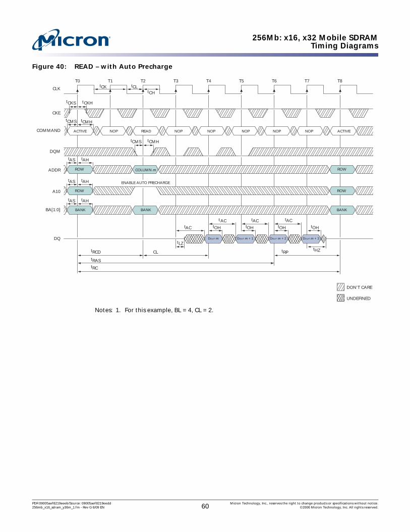
256Mb: x16, x32 Mobile SDRAMTiming Diagrams
Figure 40: READ – with Auto Precharge
Notes: 1. For this example, BL = 4, CL = 2.
t CH
t CL t CK
t AC
t LZ
t RP
t RAS
t RCD CL
t RC
CKE
CLK
DQ
A10
t OH
DOUT m
t CMH t CMS
t AH t AS
t AH t AS
t AH t AS
ROW
ROW
BANK BANK
ROW
ROW
BANK
t HZ
t OH
DOUT m + 3
t AC t OH
t AC t OH
t AC
DOUT m + 2 DOUT m + 1
COMMAND
t CMH t CMS
NOP NOP NOP NOP ACTIVE NOP READ NOP ACTIVE
ENABLE AUTO PRECHARGE
DON’T CARE
UNDEFINED
tCKH t CKS
COLUMN m
T0 T1 T2 T4 T3 T5 T6 T7 T8
BA[1:0]
DQM
ADDR
PDF:09005aef8219eeeb/Source: 09005aef8219eedd Micron Technology, Inc., reserves the right to change products or specifications without notice.256mb_x16_sdram_y36m_1.fm - Rev G 6/09 EN 60 ©2006 Micron Technology, Inc. All rights reserved.
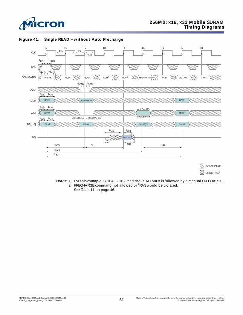
256Mb: x16, x32 Mobile SDRAMTiming Diagrams
Figure 41: Single READ – without Auto Precharge
Notes: 1. For this example, BL = 4, CL = 2, and the READ burst is followed by a manual PRECHARGE. 2. PRECHARGE command not allowed or tRAS would be violated.
See Table 11 on page 46.
ALL BANKS
t CH
t CL t CK
t AC
t LZ
t RP
t RAS
t RCD CL
t RC
CKE
CLK
DQ
A10
t OH
DOUT m
t CMH t CMS
t AH t AS
t AH t AS
t AH t AS
ROW
ROW
BANK BANK(S) BANK
ROW
ROW
BANK
t HZ
COMMAND
t CMH t CMS
NOP NOP2 NOP2 PRECHARGE ACTIVE NOP READ ACTIVE NOP
DISABLE AUTO PRECHARGE SINGLE BANK
DON’T CARE
UNDEFINED
tCKH t CKS
COLUMN m
T0 T1 T2 T4 T3 T5 T6 T7 T8
BA[1:0]
DQM
ADDR
PDF:09005aef8219eeeb/Source: 09005aef8219eedd Micron Technology, Inc., reserves the right to change products or specifications without notice.256mb_x16_sdram_y36m_1.fm - Rev G 6/09 EN 61 ©2006 Micron Technology, Inc. All rights reserved.

256Mb: x16, x32 Mobile SDRAMTiming Diagrams
Figure 42: Single READ – with Auto Precharge
Notes: 1. For this example, BL = 4, CL = 2, and the READ burst is followed by a manual PRECHARGE. 2. PRECHARGE command not allowed or tRAS would be violated.
See Table 11 on page 46.
t CH
t CL t CK
t AC
t RP t RAS
t RCD CL
t RC
CKE
CLK
DQ
A10
t OH
DOUT m
t CMH t CMS
t AH t AS
t AH t AS
t AH t AS
ROW
ROW
BANK BANK
ROW
ROW
BANK
tHZ
COMMAND
t CMH t CMS
NOP NOP NOP2 NOP2 READ ACTIVE NOP ACTIVE NOP
ENABLE AUTO PRECHARGE
DON’T CARE
UNDEFINED
tCKH t CKS
COLUMN m
T0 T1 T2 T4 T3 T5 T6 T7 T8
BA[1:0]
DQM
ADDR
PDF:09005aef8219eeeb/Source: 09005aef8219eedd Micron Technology, Inc., reserves the right to change products or specifications without notice.256mb_x16_sdram_y36m_1.fm - Rev G 6/09 EN 62 ©2006 Micron Technology, Inc. All rights reserved.
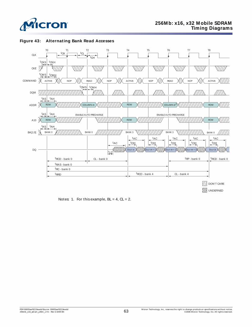
256Mb: x16, x32 Mobile SDRAMTiming Diagrams
Figure 43: Alternating Bank Read Accesses
Notes: 1. For this example, BL = 4, CL = 2.
DON’T CARE
UNDEFINED
ENABLE AUTO PRECHARGE
t CH
t CL t CK
t AC
t LZ
CLK
DQ
A10
t OH
DOUT m
t CMH t CMS
t AH t AS
t AH t AS
t AH t AS
ROW
ROW
ROW
ROW
t OH
DOUT m + 3
t AC t OH
t AC t OH
t AC
DOUT m + 2 DOUT m + 1
COMMAND
t CMH t CMS
NOP NOP ACTIVE NOP READ NOP ACTIVE
t OH
DOUT b
t AC t AC
READ
ENABLE AUTO PRECHARGE
ROW
ACTIVE
ROW
BANK 0 BANK 0 BANK 3 BANK 3 BANK 0
CKE
t CKH t CKS
COLUMN m
COLUMN b 2
T0 T1 T2 T4 T3 T5 T6 T7 T8
t RP - bank 0
t RAS - bank 0
t RCD - bank 0 t RCD - bank 0 CL - bank 0
t RCD - bank 4 CL - bank 4
t
t
RC - bank 0
RRD
BA[1:0]
DQM
ADDR
PDF:09005aef8219eeeb/Source: 09005aef8219eedd Micron Technology, Inc., reserves the right to change products or specifications without notice.256mb_x16_sdram_y36m_1.fm - Rev G 6/09 EN 63 ©2006 Micron Technology, Inc. All rights reserved.

256Mb: x16, x32 Mobile SDRAMTiming Diagrams
Figure 44: READ – Continuous Page Burst
Notes: 1. For this examples, CL = 2.2. Page left open; no tRP.
t CH
t CL t CK
t AC
t LZ
t RCD CAS Latency
DQM/ DQML, DQMH
CKE
CLK
Address
DQ
BA[1:0]
A10
t OH
DOUT m
t CMH t CMS
t AH t AS
t AH t AS
t AC t OH
DOUT m+1
ROW
ROW
t HZ
t AC t OH
DOUT m+1
t AC t OH
DOUT m+2
t AC t OH
DOUT m-1
t AC t OH
Dout m
Continuous-page burst does not self-terminateCan use BURST TERMINATE command
( ) ( )
( ) ( )
( ) ( )
( ) ( )
( ) ( )
( ) ( )
( ) ( )
Continuous page completed
1024 (x16) locations within same row
Don’t Care
Undefined
Command
t CMH t CMS
NOP NOP NOP ACTIVE NOP READ NOP BURST TERM NOP NOP
( ) ( )
( ) ( )
NOP
( ) ( )
( ) ( )
t AH t AS
BANK
( ) ( )
( ) ( )
BANK
t CKH t CKS ( ) ( )
( ) ( )
( ) ( )
( ) ( )
COLUMN m
2
T0 T1 T2 T4 T3 T5 T6 Tn + 1 Tn + 2 Tn + 3 Tn + 4
PDF:09005aef8219eeeb/Source: 09005aef8219eedd Micron Technology, Inc., reserves the right to change products or specifications without notice.256mb_x16_sdram_y36m_1.fm - Rev G 6/09 EN 64 ©2006 Micron Technology, Inc. All rights reserved.

256Mb: x16, x32 Mobile SDRAMTiming Diagrams
Figure 45: READ – DQM Operation
Notes: 1. For this example, CL = 2.
t CH
t CL t CK
t AC
t AC
t LZ
t RCD CL
CKE
CLK
DQ
A10
t OH
DOUT m
t CMH t CMS
t AH t AS
t AH t AS
t AH t AS
ROW
BANK
ROW
BANK
t HZ
t AC
t LZ
t OH
DOUT m + 2
t OH
DOUT m + 3
t HZ
COMMAND
t CMH t CMS
NOP NOP NOP NOP ACTIVE NOP READ NOP NOP
DISABLE AUTO PRECHARGE
ENABLE AUTO PRECHARGE
DON’T CARE
UNDEFINED
tCKH t CKS
COLUMN m
T0 T1 T2 T4 T3 T5 T6 T7 T8
BA[1:0]
DQM
ADDR
PDF:09005aef8219eeeb/Source: 09005aef8219eedd Micron Technology, Inc., reserves the right to change products or specifications without notice.256mb_x16_sdram_y36m_1.fm - Rev G 6/09 EN 65 ©2006 Micron Technology, Inc. All rights reserved.

256Mb: x16, x32 Mobile SDRAMTiming Diagrams
Figure 46: WRITE – Without Auto Precharge
Notes: 1. For this example, BL = 4, and the WRITE burst is followed by a manual PRECHARGE.2. 15ns is required between <DIN m + 3> and the PRECHARGE command, regardless of fre-
quency.
DISABLE AUTO PRECHARGE
ALL BANKS
t CH
t CL t CK
t RP t RAS
t RCD
t RC
CKE
CLK
DQ
A10
t CMH t CMS
t AH t AS
ROW
BANK BANK
ROW
BANK
tWR2
DON’T CARE
DIN m
t DH t DS
DIN m + 1 DIN m + 2 DIN m + 3
COMMAND
t CMH t CMS
NOP NOP NOP ACTIVE NOP WRITE PRECHARGE NOP NOP
ROW
BANK
ROW
t AH t AS
t AH t AS
t DH t DS t DH t DS t DH t DS
SINGLE BANK
t CKH t CKS
COLUMN m
T0 T1 T2 T4 T3 T5 T6 T7 T8 T9
DQM
BA[1:0]
ADDR
ACTIVE
PDF:09005aef8219eeeb/Source: 09005aef8219eedd Micron Technology, Inc., reserves the right to change products or specifications without notice.256mb_x16_sdram_y36m_1.fm - Rev G 6/09 EN 66 ©2006 Micron Technology, Inc. All rights reserved.

256Mb: x16, x32 Mobile SDRAMTiming Diagrams
Figure 47: WRITE – with Auto Precharge
Notes: 1. For this example, BL = 4.
ENABLE AUTO PRECHARGE
t CH
t CL t CK
t RP t RAS
t RCD
t RC
CKE
CLK
DQ
A10
t CMH t CMS
t AH t AS
ROW
BANK
ROW
BANK
tWR2
DON’T CARE
UNDEFINED
DIN m
t DH t DS
DIN m + 1 DIN m + 2 DIN m + 3
COMMAND
t CMH t CMS
NOP NOP NOP ACTIVE NOP WRITE NOP NOP NOP
ROW
BANK
ROW
t AH t AS
t AH t AS
t DH t DS t DH t DS t DH t DS
t CKH t CKS
COLUMN m
T0 T1 T2 T4 T3 T5 T6 T7 T8 T9
DQM
BA[1:0]
ADDR
ACTIVE
PDF:09005aef8219eeeb/Source: 09005aef8219eedd Micron Technology, Inc., reserves the right to change products or specifications without notice.256mb_x16_sdram_y36m_1.fm - Rev G 6/09 EN 67 ©2006 Micron Technology, Inc. All rights reserved.

256Mb: x16, x32 Mobile SDRAMTiming Diagrams
Figure 48: Single WRITE – Without Auto Precharge
Notes: 1. For this example, BL = 1, and the WRITE burst is followed by a manual PRECHARGE. 2. 15ns is required between <DIN m> and the PRECHARGE command, regardless of frequency. 3. PRECHARGE command not allowed or tRAS would be violated.
See Table 11 on page 46.
ALL BANKS
t CH
t CL t CK
t RP
t RAS
t RCD tWR2
t RC
CKE
CLK
DQ
A10
t CMH t CMS
t AH t AS
t AH t AS
t AH t AS
ROW
BANK BANK BANK
ROW
ROW
BANK
COMMAND
t CMH t CMS
NOP NOP3 NOP3 PRECHARGE ACTIVE NOP WRITE ACTIVE NOP
DISABLE AUTO PRECHARGE SINGLE BANK
DON’T CARE
tCKH t CKS
COLUMN m
T0 T1 T2 T4 T3 T5 T6 T7 T8
BA[1:0]
DQM
ADDR
DIN m
t DH t DS
PDF:09005aef8219eeeb/Source: 09005aef8219eedd Micron Technology, Inc., reserves the right to change products or specifications without notice.256mb_x16_sdram_y36m_1.fm - Rev G 6/09 EN 68 ©2006 Micron Technology, Inc. All rights reserved.
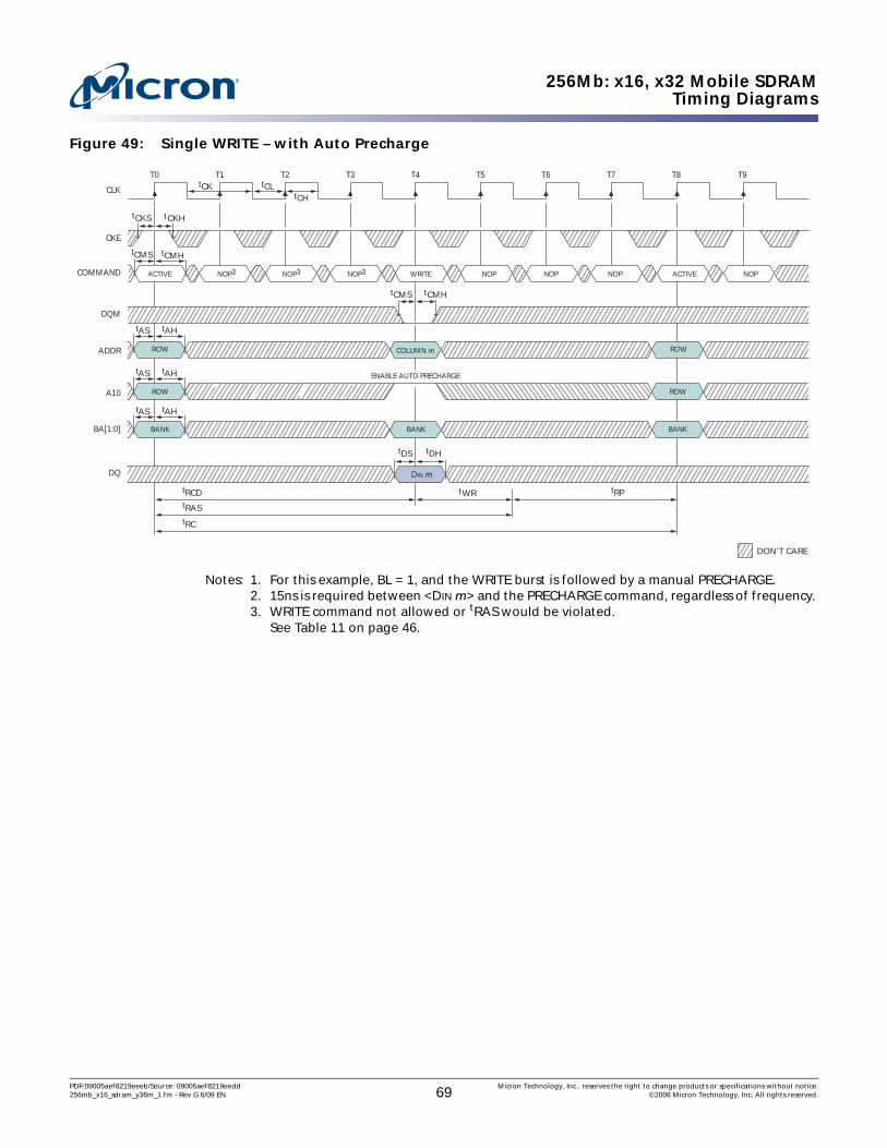
256Mb: x16, x32 Mobile SDRAMTiming Diagrams
Figure 49: Single WRITE – with Auto Precharge
Notes: 1. For this example, BL = 1, and the WRITE burst is followed by a manual PRECHARGE. 2. 15ns is required between <DIN m> and the PRECHARGE command, regardless of frequency. 3. WRITE command not allowed or tRAS would be violated.
See Table 11 on page 46.
t CH
t CL t CK
CKE
CLK
DQ
A10
t CMH t CMS
t AH t AS
t AH t AS
t AH t AS
ROW
ROW
BANK BANK
ROW
ROW
BANK
COMMAND
t CMH t CMS
NOP NOP NOP3 NOP3 WRITE ACTIVE NOP3 NOP ACTIVE NOP
ENABLE AUTO PRECHARGE
DON’T CARE
tCKH t CKS
COLUMN m
T0 T1 T2 T4 T3 T5 T6 T7 T8 T9
BA[1:0]
DQM
ADDR
t RP t RAS
t RCD
t RC
tWR
DIN m
t DH t DS
PDF:09005aef8219eeeb/Source: 09005aef8219eedd Micron Technology, Inc., reserves the right to change products or specifications without notice.256mb_x16_sdram_y36m_1.fm - Rev G 6/09 EN 69 ©2006 Micron Technology, Inc. All rights reserved.
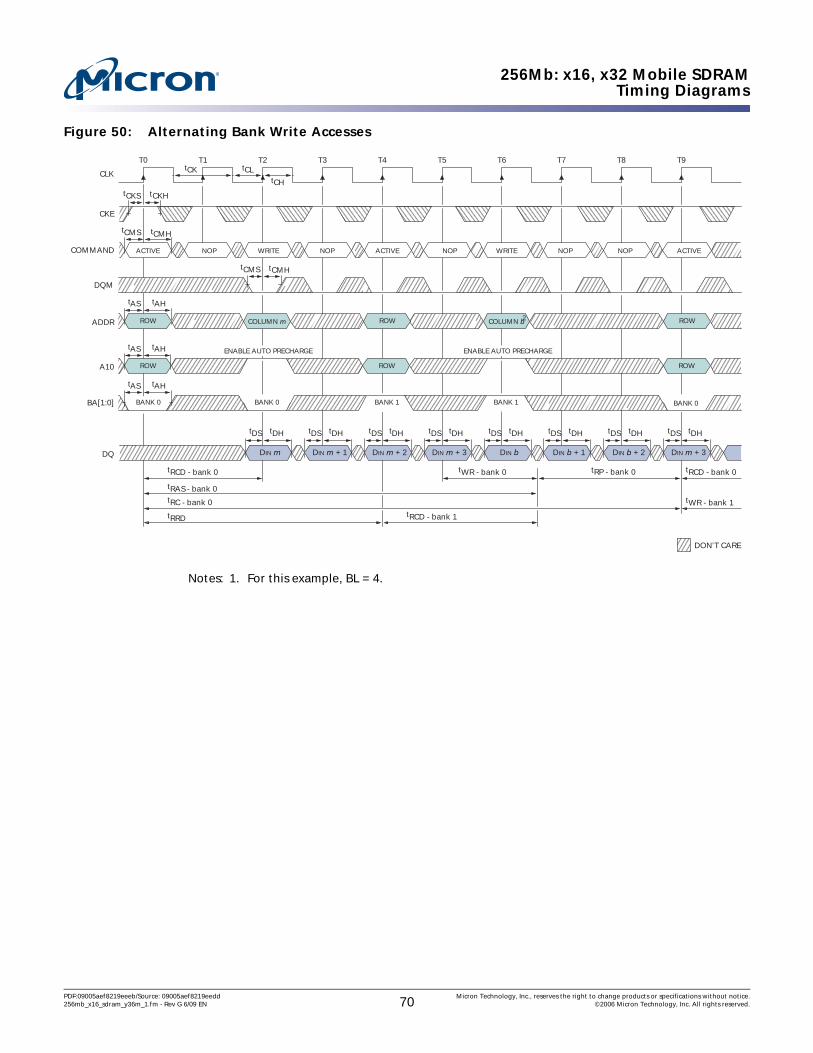
256Mb: x16, x32 Mobile SDRAMTiming Diagrams
Figure 50: Alternating Bank Write Accesses
Notes: 1. For this example, BL = 4.
DON’T CARE
ENABLE AUTO PRECHARGE
t CH
t CL t CK CLK
DQ
A10
t CMH t CMS
t AH t AS
t AH t AS
t AH t AS
ROW
ROW
ROW
ROW
COMMAND
t CMH t CMS
NOP NOP ACTIVE NOP WRITE NOP NOP ACTIVE WRITE
ENABLE AUTO PRECHARGE
ROW
ACTIVE
ROW
BANK 0 BANK 0 BANK 1 BANK 1 BANK 0
CKE
t CKH t CKS
COLUMN m
COLUMN b2
T0 T1 T2 T4 T3 T5 T6 T7 T8 T9
t RP - bank 0
t RAS - bank 0
t RCD - bank 0 t RCD - bank 0
t WR - bank 1
t WR - bank 0
t RCD - bank 1
t
t
RC - bank 0
RRD
BA[1:0]
DQM
ADDR
DIN m
t DH t DS
DIN m + 1 DIN m + 2 DIN m + 3
t DH t DS t DH t DS t DH t DS
DIN b
t DH t DS
DIN b + 1
t DH t DS
DIN b + 2
t DH t DS
DIN m + 3
t DH t DS
PDF:09005aef8219eeeb/Source: 09005aef8219eedd Micron Technology, Inc., reserves the right to change products or specifications without notice.256mb_x16_sdram_y36m_1.fm - Rev G 6/09 EN 70 ©2006 Micron Technology, Inc. All rights reserved.
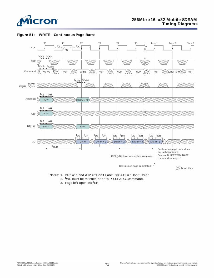
256Mb: x16, x32 Mobile SDRAMTiming Diagrams
Figure 51: WRITE – Continuous Page Burst
Notes: 1. x16: A11 and A12 = “Don’t Care”; x8: A12 = “Don’t Care.” 2. tWR must be satisfied prior to PRECHARGE command. 3. Page left open; no tRP.
t CH
t CL t CK
t RCD
DQM/ DQML, DQMH
CKE
CLK
Addresss
BA[1:0]
A10
t CMS
t AH t AS
t AH t AS
ROW
ROW
Continuous-page burst doesnot self-terminate. Can use BURST TERMINATE command to stop.2, 3
( ) ( )
( ) ( )
( ) ( )
( ) ( )
Continuous page completedDon’t Care
Command
t CMH t CMS
NOP NOP NOP ACTIVE NOP WRITE BURST TERM NOP NOP
( ) ( )
( ) ( )
DQ DIN m
t DH t DS
DIN m + 1 DIN m + 2 DIN m + 3
t DH t DS t DH t DS t DH t DS
DIN m - 1
t DH t DS
t AH t AS
BANK
( ) ( )
( ) ( )
BANK
t CMH
t CKH t CKS
( ) ( )
( ) ( )
( ) ( )
( ) ( )
( ) ( )
( ) ( )
1024 (x16) locations within same row
COLUMN m1
T0 T1 T2 T3 T4 T5 Tn + 1 Tn + 2 Tn + 3
( ) ( )
( ) ( )
PDF:09005aef8219eeeb/Source: 09005aef8219eedd Micron Technology, Inc., reserves the right to change products or specifications without notice.256mb_x16_sdram_y36m_1.fm - Rev G 6/09 EN 71 ©2006 Micron Technology, Inc. All rights reserved.
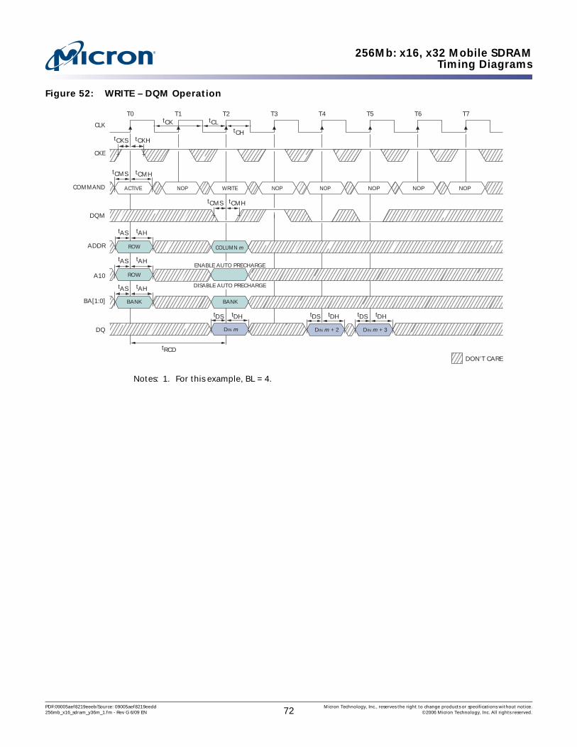
256Mb: x16, x32 Mobile SDRAMTiming Diagrams
Figure 52: WRITE – DQM Operation
Notes: 1. For this example, BL = 4.
DON’T CARE
t CH
t CL t CK
t RCD
CKE
CLK
DQ
A10
t CMS
t AH t AS
ROW
BANK
ROW
BANK
ENABLE AUTO PRECHARGE
DIN m + 3
t DH t DS
DIN m DIN m + 2
t CMH
COMMAND NOP NOP NOP ACTIVE NOP WRITE NOP NOP
t CMS t CMH
t DH t DS t DH t DS
t AH t AS
t AH t AS
DISABLE AUTO PRECHARGE
t CKH t CKS
COLUMN m
T0 T1 T2 T3 T4 T5 T6 T7
BA[1:0]
DQM
ADDR
PDF:09005aef8219eeeb/Source: 09005aef8219eedd Micron Technology, Inc., reserves the right to change products or specifications without notice.256mb_x16_sdram_y36m_1.fm - Rev G 6/09 EN 72 ©2006 Micron Technology, Inc. All rights reserved.

256Mb: x16, x32 Mobile SDRAMPackage Dimensions
Package Dimensions
Figure 53: 54-Ball VFBGA (8mm x 9mm)
Notes: 1. All dimensions are in millimeters.
MICRON LOGO TO BE LASED BALL A1 ID
SUBSTRATE MATERIAL: PLASTIC LAMINATE MOLD COMPOUND: EPOXY NOVOLAC
SOLDER BALL MATERIAL: SAC105 (98.5% Sn, 1% Ag, 0.5% Cu)
SEATING PLANE
0.65 ±0.05
BALL A9
SOLDER BALL DIAMETER REFERS TO POST REFLOW
CONDITION. THE PRE- REFLOW DIAMETER
IS 0.42 ON A 0.40 SMD BALL PAD.
0.10 A A
9.00 ± 0.10
0.80 TYP
4.50 ±0.05
1.00 MAX
3.20
6.40
BALL A1 ID BALL A1
0.80 TYP
8.00 ±0.10
3.20 4.00 ±0.05
6.40
54X Ø0.45
C L
C L
PDF:09005aef8219eeeb/Source: 09005aef8219eedd Micron Technology, Inc., reserves the right to change products or specifications without notice.256mb_x16_sdram_y36m_1.fm - Rev G 6/09 EN 73 ©2006 Micron Technology, Inc. All rights reserved.
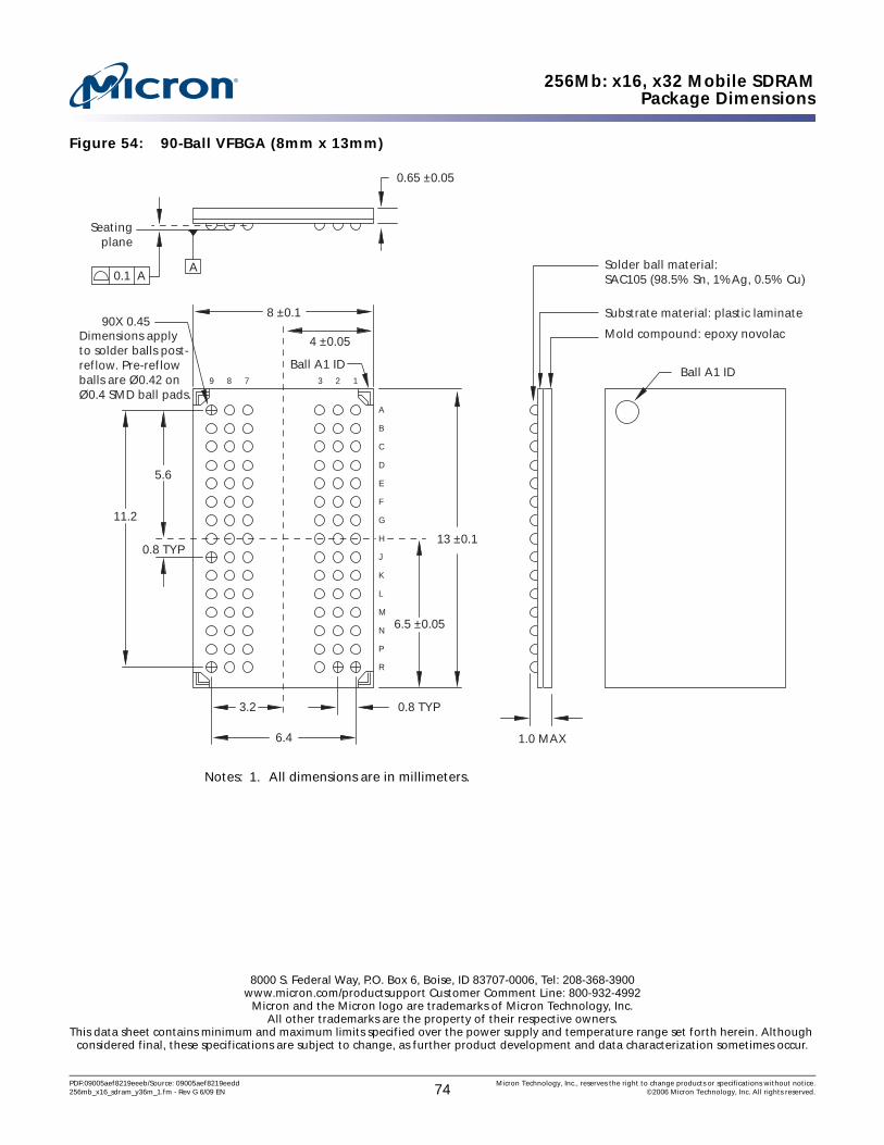
256Mb: x16, x32 Mobile SDRAMPackage Dimensions
Figure 54: 90-Ball VFBGA (8mm x 13mm)
Notes: 1. All dimensions are in millimeters.
Ball A1 ID
1.0 MAX
Mold compound: epoxy novolac
Substrate material: plastic laminate
Solder ball material:SAC105 (98.5% Sn, 1%Ag, 0.5% Cu)
13 ±0.1
Ball A1 ID9 8 7 3 2 1
A
B
C
D
E
F
G
H
J
K
L
M
N
P
R
0.8 TYP
6.5 ±0.05
8 ±0.1
4 ±0.05
3.2
5.6
0.65 ±0.05
Seatingplane
A
11.2
6.4
0.1 A
90X 0.45Dimensions applyto solder balls post-reflow. Pre-reflowballs are Ø0.42 onØ0.4 SMD ball pads.
0.8 TYP
8000 S. Federal Way, P.O. Box 6, Boise, ID 83707-0006, Tel: 208-368-3900www.micron.com/productsupport Customer Comment Line: 800-932-4992
Micron and the Micron logo are trademarks of Micron Technology, Inc.All other trademarks are the property of their respective owners.
This data sheet contains minimum and maximum limits specified over the power supply and temperature range set forth herein. Although considered final, these specifications are subject to change, as further product development and data characterization sometimes occur.
PDF:09005aef8219eeeb/Source: 09005aef8219eedd Micron Technology, Inc., reserves the right to change products or specifications without notice.256mb_x16_sdram_y36m_1.fm - Rev G 6/09 EN 74 ©2006 Micron Technology, Inc. All rights reserved.
256Mb: x16, x32 Mobile SDRAMRevision History
Revision History
Rev. G, Production . . . . . . . . . . . . . . . . . . . . . . . . . . . . . . . . . . . . . . . . . . . . . . . . . . . . . . . . . . . . . . . . . . . . . . . . . . . . . . . . . . 06/09
• Table 10, “DC Electrical Characteristics and Operating Conditions,” on page 45: Updated IOZ specification.
Rev. F, Production . . . . . . . . . . . . . . . . . . . . . . . . . . . . . . . . . . . . . . . . . . . . . . . . . . . . . . . . . . . . . . . . . . . . . . . . . . . . . . . . . . . 04/07
• Changed wording in Note 1 in the “Options” section on page 1.• Changed CL = 2, -75 and -8 access times from “6ns” and “7ns” to “9ns” in Table 2 on
page 1.• Added “Revision :G” to Figure 1 on page 5.• Changed refresh counter from “12” to “13” and changed Bank0 Memory Array from
“8,192” to “4,096” in Figure 3 on page 7.• Changed E2, K2 to “DNU” and added the following sentence in the: “TEST pin must
be tied to VssQ in normal operation” in Table 3 on page 10.• Added the following sentence to the “Input/output mask” description in Table 3 on
page 10: “DQM loading is designed to match that of DQ balls.”• Removed all the text after the first sentence in the “Initialization” section on page 12. • Removed the first seven words in the “Mode Register” section on page 13.• Removed “(sequential or interleaved)” and “...the specified time...” in the
“Mode Register” section on page 13.• Changed “M13” and “M12” to “M13” and “M14” and deleted a column in the
“Operating Mode” table in Figure 3 on page 7.• Removed the notes under Table 4 on page 15.• Corrected the “Operating Mode” table in Figure 6 on page 14.• Removed the following text under the “Operating Mode” section on page 16: “or test
modes” and “The programmed BL applies to both READ and WRITE bursts.”• Removed “(nonburst)” under the “Write Burst Mode” section on page 16.• Removed the last two sentences in the first paragraph and removed
“(BA1=1, AB0=0),” in the second paragraph in the “Low-Power Extended Mode Regis-ter (EMR) Definition” section on page 16.
• Changed the “Low-Power Extended Mode Register (EMR) Definition” heading to “Extended Mode Register (EMR)” on page 16.
• Moved Figure 7 to page 16.• Changed the title of Figure 7 on page 16 to “EMR Definition.” • Removed all bank address references from the “PASR Self-Refresh Coverage” in
Figure 7 on page 16.• Replace the “Temperature-Compensated Self Refresh (TCSR)” section on page 17.• Removed the second sentence in the “Partial Array Self-Refresh” section on page 18.• Replaced Table 5 on page 19 and all the associated notes.• Removed last paragraph and added “A0–A12” in the first sentence in the “Load Mode
Register” section on page 20.• Removed “...and the DQ balls tri-state” from the “COMMAND INHIBIT” section on
page 19.• Moved the “Auto Precharge” section to page 21.• Added a second paragraph in the “Deep Power Down” section on page 22.• Added “BL = 2” to the note under Figure 20 on page 31.• Added “BL = 2” to the note under Figure 22 on page 32.• Changed “(see Figure 23)” to “(see Figure 25)” on page 34.
PDF:09005aef8219eeeb/Source: 09005aef8219eedd Micron Technology, Inc., reserves the right to change products or specifications without notice.256mb_x16_sdram_y36m_1.fm - Rev G 6/09 EN 75 ©2006 Micron Technology, Inc. All rights reserved.
256Mb: x16, x32 Mobile SDRAMRevision History
• Moved Figure 25 to page 34.• Removed the “In order to exit deep power down...” paragraph on page 35.• Replaced text in note 9 and removed “Deep power down” rows in Table 7 on page 41.• Added note 9 to tAC and note 27 to tOHN in Table 11 on page 46.• Changed tXSR from “67.5” to “80” in Table 11 on page 46.• Changed “9” to “8” for tAC (2) -75, and tCK (2) -75 from “10” to “9” in Table 11 on
page 46.• Replaced note 30 and 31 in the “Notes” section on page 52.• Moved Figure 34 to page 54.• Removed note 1 from Figure 38 on page 58.
Rev. E, Production. . . . . . . . . . . . . . . . . . . . . . . . . . . . . . . . . . . . . . . . . . . . . . . . . . . . . . . . . . . . . . . . . . . . . . . . . . . . . . . . . . . 03/07
• Changed ball D7 from “VDDQ” to “VSSQ” in Figure 4 on page 8.Rev. D, Production . . . . . . . . . . . . . . . . . . . . . . . . . . . . . . . . . . . . . . . . . . . . . . . . . . . . . . . . . . . . . . . . . . . . . . . . . . . . . . . . . . 02/07
• Removed CL = 1 from Table 2 on page 1, Figure 6 on page 14, Figure 7 on page 16, Figure 12 on page 25, Figure 13 on page 26, Figure 16 on page 28, Figure 17 on page 29, Table 11 on page 46, Table 12 on page 47.
Rev. C, Production . . . . . . . . . . . . . . . . . . . . . . . . . . . . . . . . . . . . . . . . . . . . . . . . . . . . . . . . . . . . . . . . . . . . . . . . . . . . . . . . . . 09/06
• Added a “For burst length of 16 or continuous page burst, contact factory for avail-ability” in Features section on page 1.
• Changed “Burst Length = 1” in the IDD1 row in Table 13 and Table 14.• Changed all instances of “HDQM” with “UDQM.” • Changed all instances of “DQM0-3” to “DQM” in Figure 36 through Figure 52.• Removed all instances of continuous page burst after page 1.• Added changed burst length “16” and “continuous” to “Reserved” in Figure 6.• Removed note specifying “E14 and E13 (BA1 and BA0) must be “1, 0” to select the
extended mode register (vs. the standard mode register) from Figure 8.• Changed the following sentence in the “Extended Mode Register (EMR)” on page 16:
“The low-power EMR must be loaded when all banks are idle and no burst are in progress.”
• Removed the following note from Figure 53 and Figure 54: “Green packaging compo-sition is available upon request.”
Rev. B, Production . . . . . . . . . . . . . . . . . . . . . . . . . . . . . . . . . . . . . . . . . . . . . . . . . . . . . . . . . . . . . . . . . . . . . . . . . . . . . . . . . . 09/06
• Added Note 1 to Figure 8, page 17.• Updated Table 15 values, page 50.• Removed all instances of -10 speed grade.• Changed CL = 2 from 104 MHz to 100 MHz.• Changed “Refresh count” for 8 Meg x 32 to 8K from 4K in Table 1.• Added “E2” row to Table 3.• Removed the following from sentence two in the “General Description” section: “This
architecture is compatible with the 2n rule of prefetch architecture.”• Removed all instances of “full” page burst and replaced them with “continuous” page
burst.• Added the following note to the “Features” section on page 1: “Contact factory for
availability.”• Added a “Power” section to “Options” on page 1.• Replaced old part numbering table with Figure 1.• Changed the clock rate on -75 and -8 for CL = 2 from 111 to 100 in Table 2.
PDF:09005aef8219eeeb/Source: 09005aef8219eedd Micron Technology, Inc., reserves the right to change products or specifications without notice.256mb_x16_sdram_y36m_1.fm - Rev G 6/09 EN 76 ©2006 Micron Technology, Inc. All rights reserved.
256Mb: x16, x32 Mobile SDRAMRevision History
• Changed the “8” address lines going into the “column address counter/Latch” to “9” in Figure 2.
• Changed all references of 13 to 12 and changed the “8” address lines going into the “column address counter/Latch” to “9” in Figure 3.
• Changed the “8” address lines going into the “column address counter/Latch” to “9” in Figure 2.
• Deleted “(4 Meg x32 x4 banks)” from the first sentence of the “Functional Descrip-tion” section.
• Removed the following sentence from the “Mode Register (MR) section: “M12 and M13 should be set to zero to prevent the EMR from being programmed.”
• Added A12 to Figure 6.• Added notes 2? and 2 to Figure 8.• Removed Table 5, “CAS Latency.”• Removed all notes except note 2 and added note 1 to Table 5.• Removed all text references to the “2n rule.”• Changed the following items in Table 12: Changed tAC(2) from 7/8 to 9ns for -75 and -
8 speed grades, changed tCK(2) from 9 tp 10ns for -75 and -8 speed grades, and changed tHZ(2) from 7/8 to 9ns for -75 and -8 speed grades.
• Added Table 14 for x32 specifications.• Changed the following specifications in Table 16: CLK 1.5 (MIN) 4.5 (MAX), Input 2.0
(MIN) 4.5 (MAX), DQs 2.0 (MIN) 6.0 (MAX)• Added Figure 33.• Deleted first line of “Solder Ball Material” in Figure 52.• Changed “Burst Length = 1” in the IDD1 row in Table 13 and Table 14.• Added a “Contact factory for availability” note to Figure 6.
Rev. A, Advance . . . . . . . . . . . . . . . . . . . . . . . . . . . . . . . . . . . . . . . . . . . . . . . . . . . . . . . . . . . . . . . . . . . . . . . . . . . . . . . . . . . . . 4/06
• Initial release
PDF:09005aef8219eeeb/Source: 09005aef8219eedd Micron Technology, Inc., reserves the right to change products or specifications without notice.256mb_x16_sdram_y36m_1.fm - Rev G 6/09 EN 77 ©2006 Micron Technology, Inc. All rights reserved.


