
6.976High Speed Communication Circuits and Systems
Lecture 9Low Noise Amplifiers
Michael PerrottMassachusetts Institute of Technology
Copyright © 2003 by Michael H. Perrott
M.H. Perrott MIT OCW
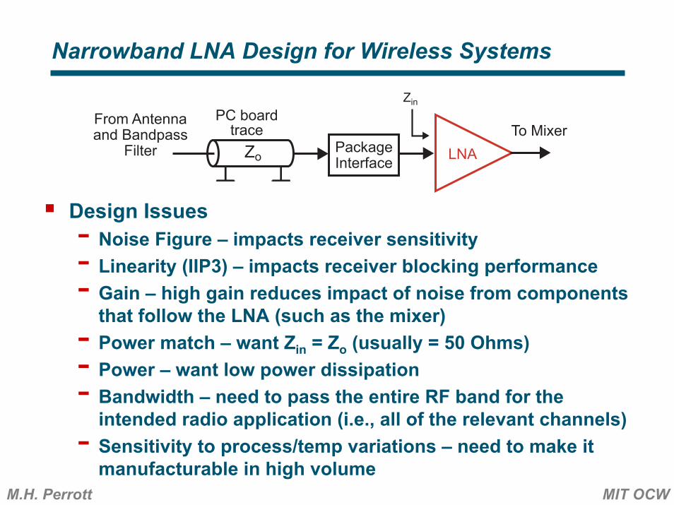
Narrowband LNA Design for Wireless Systems
Design Issues- Noise Figure – impacts receiver sensitivity- Linearity (IIP3) – impacts receiver blocking performance- Gain – high gain reduces impact of noise from components
that follow the LNA (such as the mixer)- Power match – want Zin = Zo (usually = 50 Ohms) - Power – want low power dissipation- Bandwidth – need to pass the entire RF band for the
intended radio application (i.e., all of the relevant channels)- Sensitivity to process/temp variations – need to make it
manufacturable in high volume
Zin
Zo LNATo Mixer
From Antennaand Bandpass
Filter
PC boardtrace
PackageInterface
M.H. Perrott MIT OCW
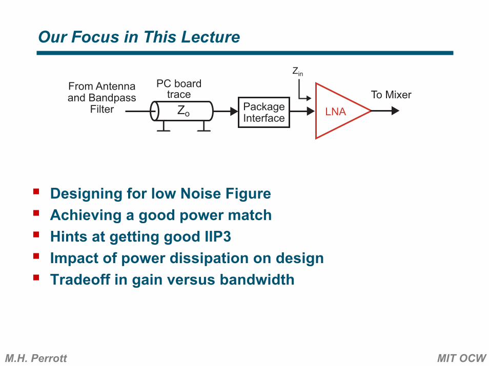
Our Focus in This Lecture
Designing for low Noise FigureAchieving a good power matchHints at getting good IIP3Impact of power dissipation on designTradeoff in gain versus bandwidth
Zin
Zo LNATo Mixer
From Antennaand Bandpass
Filter
PC boardtrace
PackageInterface

M.H. Perrott MIT OCW
Our Focus: Inductor Degenerated Amp
Same as amp in Lecture 7 except for inductor degeneration- Note that noise analysis in Tom Lee’s book does not include
inductor degeneration (i.e., Table 11.1)
vgs gmvgsCgs indgZgs
Rsens
Sourceinout
Lg
M1
Ldeg
LgRs
vin
Vbias
IoutSource
Ldeg
M.H. Perrott MIT OCW
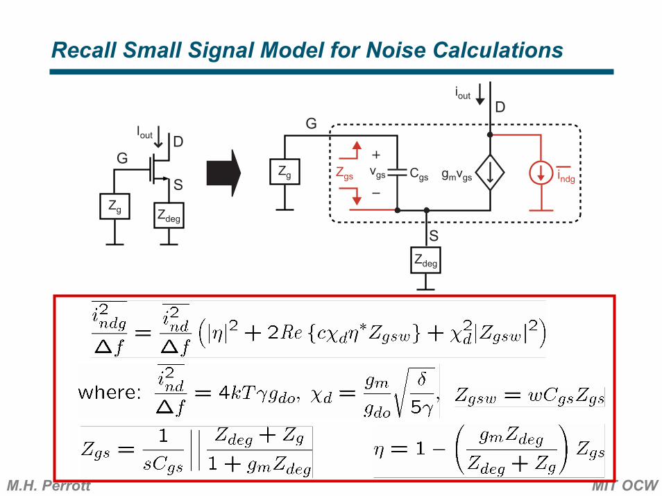
Recall Small Signal Model for Noise Calculations
Iout
GD
Svgs gmvgsCgs indg
D
S
G
ZgsZg
Zdeg
iout
Zg Zdeg
M.H. Perrott MIT OCW
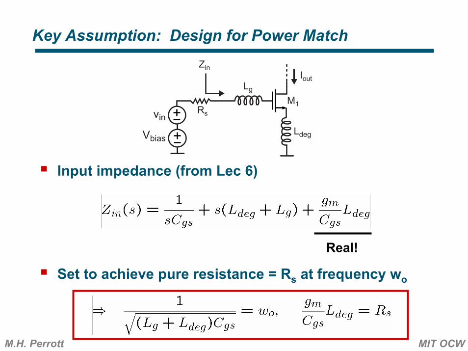
Input impedance (from Lec 6)
Set to achieve pure resistance = Rs at frequency wo
Key Assumption: Design for Power Match
M1
Vbias
vinRs
Ldeg
ZinIout
Lg
Real!

M.H. Perrott MIT OCW
Process and Topology Parameters for Noise Calculation
Process parameters- For 0.18µ CMOS, we will assume the following
Circuit topology parameters Zg and Zdeg
vgs gmvgsCgs indgZgs
Rsens
Sourceinout
Lg
Ldeg

M.H. Perrott MIT OCW
Calculation of Zgs
vgs gmvgsCgs indgZgs
Rsens
Sourceinout
Lg
Ldeg

M.H. Perrott MIT OCW
Calculation of η
vgs gmvgsCgs indgZgs
Rsens
Sourceinout
Lg
Ldeg
= Rs
M.H. Perrott MIT OCW
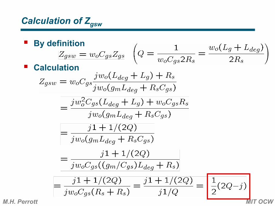
Calculation of Zgsw
By definition
Calculation
M.H. Perrott MIT OCW
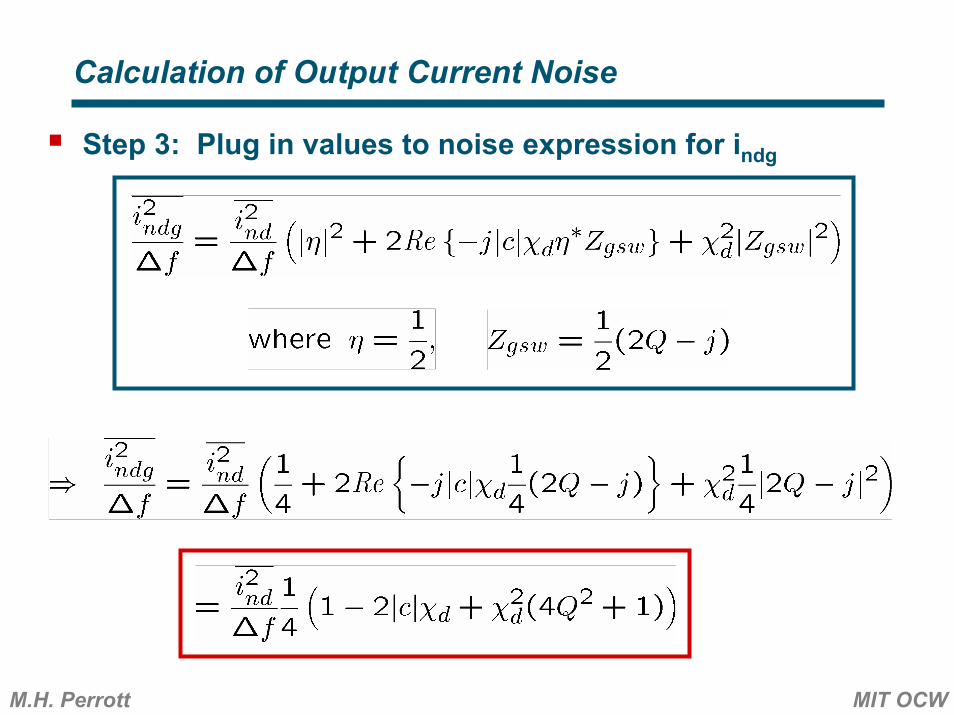
Calculation of Output Current Noise
Step 3: Plug in values to noise expression for indg

M.H. Perrott MIT OCW
From Lecture 7, we derived for Ldeg = 0, wo2 = 1/(LgCgs)
We now have for (gm/Cgs)Ldeg = Rs, wo2 = 1/((Lg + Ldeg)Cgs)
Compare Noise With and Without Inductor Degeneration
vgs gmvgsCgs indgZgs
Rsens
Sourceinout
Lg
Ldeg

M.H. Perrott MIT OCW
Recall the alternate expression for Noise Factor derived in Lecture 8
We now know the output noise due to the transistor noise- We need to determine the output noise due to the source
resistance
Derive Noise Factor for Inductor Degenerated Amp
vgs gmvgsCgs indgZgs
Rsens
Sourceinout
Lg
Ldeg

M.H. Perrott MIT OCW
Output Noise Due to Source Resistance
vgs gmvgsCgs indgZgs
Rsens
Sourceinout
Lg
Ldeg
Zin

M.H. Perrott MIT OCW
Noise Factor for Inductor Degenerated Amplifier
Noise Factor scaling coefficient

M.H. Perrott MIT OCW
Noise Factor Scaling Coefficient Versus Q
1 1.5 2 2.5 3 3.5 4 4.5 52.5
3
3.5
4
4.5
5
5.5
6
6.5
7
Q
Noi
se F
acto
r Sca
ling
Coe
ffici
ent
Noise Factor Scaling Coefficient Versus Q for 0.18 µ NMOS Device
Achievable values asa function of Q underthe constraints that
(Lg+Ldeg)Cgs
1= wo
Ldeg = RsCgs
gm
2RswoCgs
1Q =Note:
c = -j0
c = -j0.55
c = -j1
M.H. Perrott MIT OCW
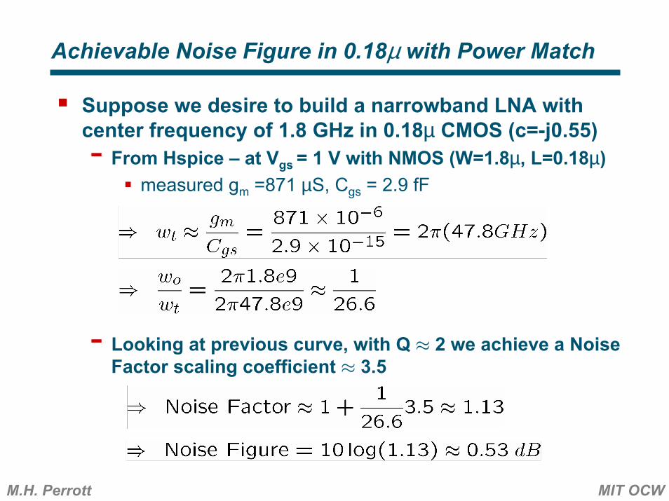
Achievable Noise Figure in 0.18µ with Power Match
Suppose we desire to build a narrowband LNA with center frequency of 1.8 GHz in 0.18µ CMOS (c=-j0.55)- From Hspice – at Vgs = 1 V with NMOS (W=1.8µ, L=0.18µ)
measured gm =871 µS, Cgs = 2.9 fF
- Looking at previous curve, with Q ≈ 2 we achieve a Noise Factor scaling coefficient ≈ 3.5

M.H. Perrott MIT OCW
Component Values for Minimum NF with Power Match
Assume Rs = 50 Ohms, Q = 2, fo = 1.8 GHz, ft = 47.8 GHz- Cgs calculated as
- Ldeg calculated as
- Lg calculated as

M.H. Perrott MIT OCW
Have We Chosen the Correct Bias Point? (Vgs = 1V)
M1
IdVgs
WL = 1.8µ
0.18µ
0 100 200 300 400 500 600 7000
0.5
1
1.5
2
2.5
3
3.5
4
4.5
Current Density (microAmps/micron)
g m a
nd g
do (m
illiAm
ps/V
olts
) and
Vgs
(Vol
ts)
Vgs , gm , and gdo versus Current Density for 0.18µ NMOS
gm
gdo
Vgs
Chosen biaspoint is Vgs = 1 V
Lower powerLower ft
Lower IIP3
Higher powerHigher ft
Higher IIP3gdogm
gdogm
Lower Higher
Note: IIP3 is also a function of Q

M.H. Perrott MIT OCW
Calculation of Bias Current for Example Design
Calculate current density from previous plot
Calculate W from Hspice simulation (assume L=0.18 µm)
- Could also compute this based on Cox valueCalculate bias current
- Problem: this is not low power!!
M.H. Perrott MIT OCW
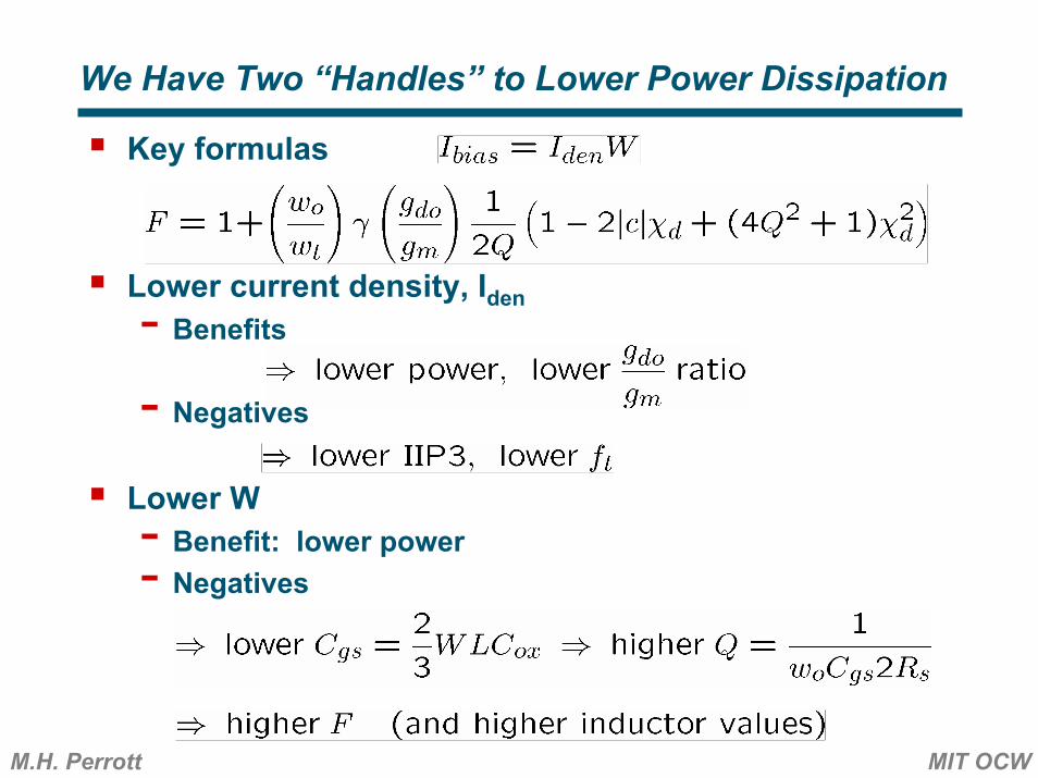
We Have Two “Handles” to Lower Power Dissipation
Key formulas
Lower current density, Iden- Benefits
- Negatives
Lower W- Benefit: lower power- Negatives
M.H. Perrott MIT OCW
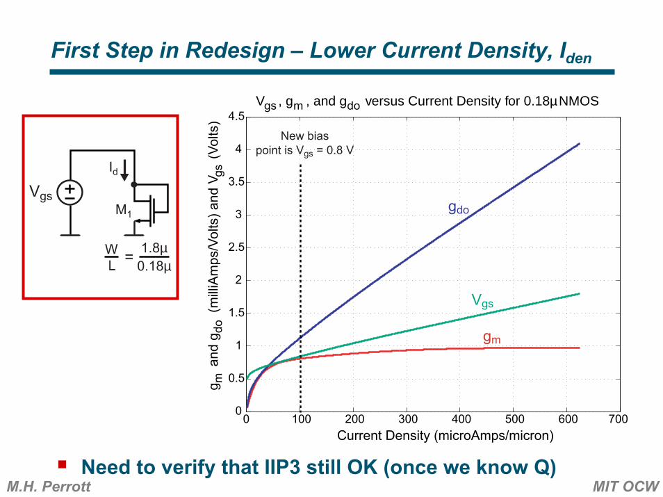
First Step in Redesign – Lower Current Density, Iden
M1
IdVgs
WL = 1.8µ
0.18µ
0 100 200 300 400 500 600 7000
0.5
1
1.5
2
2.5
3
3.5
4
4.5
Current Density (microAmps/micron)
g m a
nd g
do (m
illiAm
ps/V
olts
) and
Vgs
(Vol
ts)
Vgs , gm , and gdo versus Current Density for 0.18µ NMOS
gm
gdo
Vgs
New biaspoint is Vgs = 0.8 V
Need to verify that IIP3 still OK (once we know Q)
M.H. Perrott MIT OCW
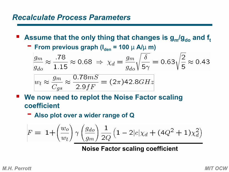
Recalculate Process Parameters
Assume that the only thing that changes is gm/gdo and ft- From previous graph (Iden = 100 µ A/µ m)
We now need to replot the Noise Factor scaling coefficient- Also plot over a wider range of Q
Noise Factor scaling coefficient
M.H. Perrott MIT OCW
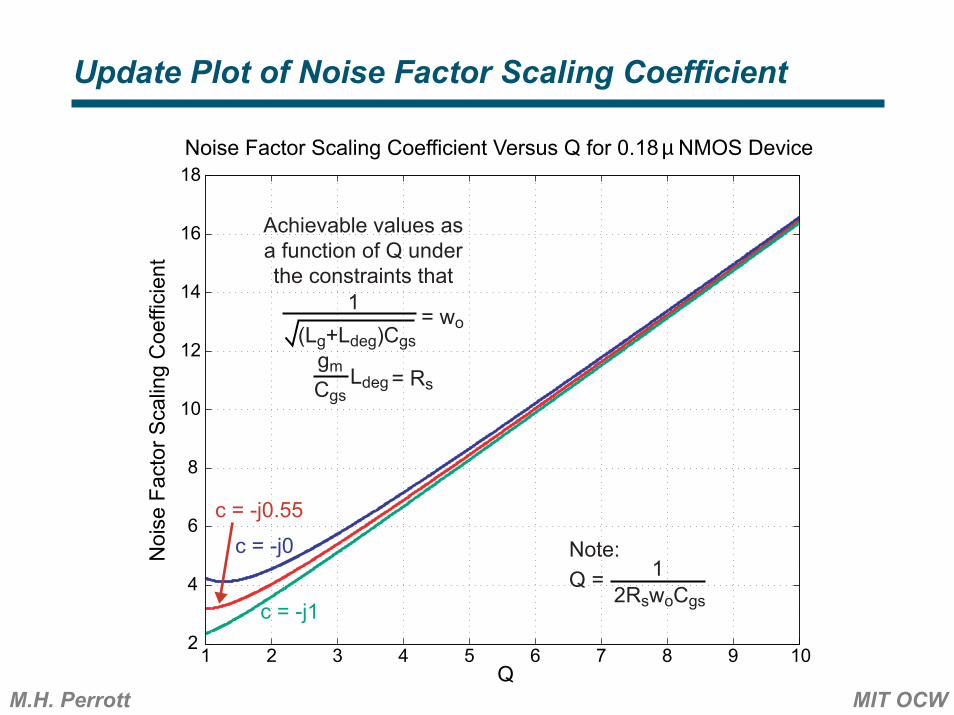
Update Plot of Noise Factor Scaling Coefficient
1 2 3 4 5 6 7 8 9 102
4
6
8
10
12
14
16
18
Q
Noi
se F
acto
r Sca
ling
Coe
ffici
ent
Noise Factor Scaling Coefficient Versus Q for 0.18 µ NMOS Device
Achievable values asa function of Q underthe constraints that
(Lg+Ldeg)Cgs
1= wo
Ldeg = RsCgs
gm
2RswoCgs
1Q =Note:c = -j0
c = -j0.55
c = -j1

M.H. Perrott MIT OCW
Second Step in Redesign – Lower W
Recall
Ibias can be related to Q as
We previously chose Q = 2, let’s now choose Q = 6- Cuts power dissipation by a factor of 3!- New value of W is one third the old one
M.H. Perrott MIT OCW
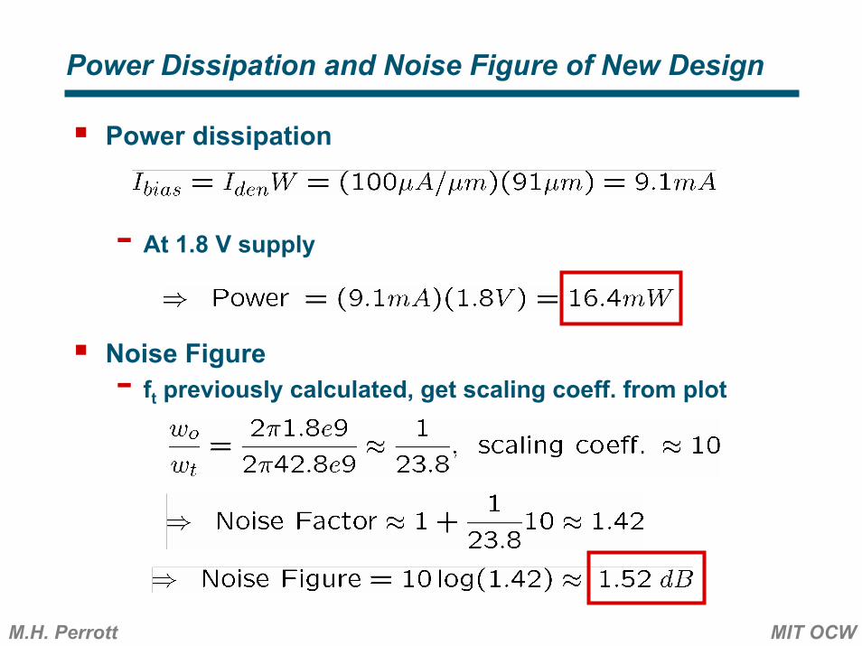
Power Dissipation and Noise Figure of New Design
Power dissipation
- At 1.8 V supply
Noise Figure- ft previously calculated, get scaling coeff. from plot

M.H. Perrott MIT OCW
Updated Component Values
Assume Rs = 50 Ohms, Q = 6, fo = 1.8 GHz, ft = 42.8 GHz- Cgs calculated as
- Ldeg calculated as
- Lg calculated as

M.H. Perrott MIT OCW
Inclusion of Load (Resonant Tank)
Add output load to achieve voltage gain- Note: in practice, use cascode device
We’re ignoring Cgd in this analysis
M1
Ldeg
LgRs
vin
Vbias
LL RL CL
VoutIout
vgs gmvgsCgs indgZgs
Rsens
inout
Lg
Ldeg
vin
iout
LL RL CL
vout
Zin

M.H. Perrott MIT OCW
Calculation of Gain
Assume Zin = Rs
Assume load tank resonates at frequency wo
vgs gmvgsCgs indgZgs
Rsens
inout
Lg
Ldeg
vin
iout
LL RL CL
vout
Zin

M.H. Perrott MIT OCW
Setting of Gain
Parameters gm and Q were set by Noise Figure and IIP3 considerations- Note that Q is of the input matching network, not the
amplifier loadRL is the free parameter – use it to set the desired gain- Note that higher RL for a given resonant frequency and
capacitive load will increase QL (i.e., Q of the amplifier load)
There is a tradeoff between amplifier bandwidth and gain- Generally set RL according to overall receiver noise and
IIP3 requirements (higher gain is better for noise)Very large gain (i.e., high QL) is generally avoided to minimize sensitivity to process/temp variations that will shift the center frequency
M.H. Perrott MIT OCW
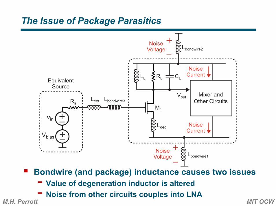
The Issue of Package Parasitics
Bondwire (and package) inductance causes two issues- Value of degeneration inductor is altered- Noise from other circuits couples into LNA
M1
Ldeg
LextRs
vin
Vbias
LL RL CL
Vout
Lbondwire1
Mixer andOther Circuits
NoiseCurrent
NoiseCurrent
Lbondwire2
Lbondwire3
EquivalentSource
NoiseVoltage
NoiseVoltage

M.H. Perrott MIT OCW
Differential LNA
Advantages- Value of Ldeg is now much better controlled- Much less sensitivity to noise from other circuits
Disadvantages- Twice the power as the single-ended version- Requires differential input at the chip
M1Ldeg
LgRs
vin
Vbias
LL RL CL
Vout
M2
LLRLCL
Vout
Ibias
Ldeg
Lg Rs
2-vin
2

M.H. Perrott MIT OCW
Note: Be Generous with Substrate Contact Placement
Having an abundance of nearby substrate contacts helps in three ways- Reduces possibility of latch up issues- Lowers Rsub and its associated noise
Impacts LNA through backgate effect (gmb)- Absorbs stray electrons from other circuits that will otherwise inject noise into the LNA
Negative: takes up a bit extra area
S DG
SubstrateContact
SubstrateContact
GND
P-
GND
N+ N+
RsubRsub
To Ldeg To LgTo amplifer
load
Hot electrons andother noise
Hot electrons andother noise
enRsub enRsub

M.H. Perrott MIT OCW
Another CMOS LNA Topology
Consider increasing gm for a given current by using both PMOS and NMOS devices- Key idea: re-use of current
Issues- PMOS device has poorer transconductance than NMOS for a given amount of current, and ft is lower- Not completely clear there is an advantage to using this technique, but published results are good
See A. Karanicolas, “A 2.7 V 900-MHz CMOS LNA and Mixer”, JSSC, Dec 1996
M1
M2
M1
Id
W/L
M2
Id/2
M1
Id/2
(1/2)W/L (1/2)W/L
Id
gm
gm1+gm2
gm1+gm2Id/2
Id/2
(1/2)W/L
(1/2)W/L
M.H. Perrott MIT OCW
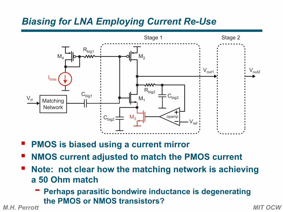
Biasing for LNA Employing Current Re-Use
PMOS is biased using a current mirrorNMOS current adjusted to match the PMOS currentNote: not clear how the matching network is achieving a 50 Ohm match- Perhaps parasitic bondwire inductance is degenerating
the PMOS or NMOS transistors?
M2
M1
Cbig2
Ibias
Rbig1M4
Rbig2
M3 opampVref
Cbig3Cbig1
MatchingNetwork
Vrf
Vout1 Vout2
Stage 1 Stage 2
M.H. Perrott MIT OCW
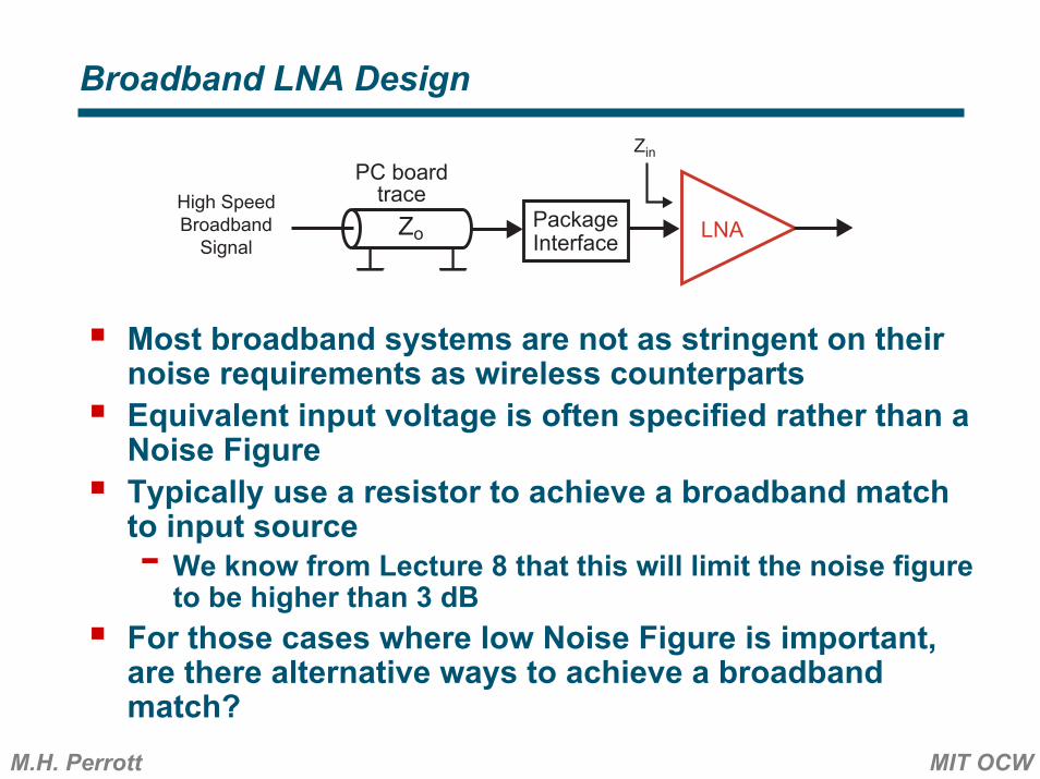
Broadband LNA Design
Most broadband systems are not as stringent on their noise requirements as wireless counterpartsEquivalent input voltage is often specified rather than a Noise FigureTypically use a resistor to achieve a broadband match to input source- We know from Lecture 8 that this will limit the noise figure
to be higher than 3 dBFor those cases where low Noise Figure is important, are there alternative ways to achieve a broadband match?
Zin
Zo LNA
PC boardtrace
PackageInterface
High SpeedBroadband
Signal
M.H. Perrott MIT OCW
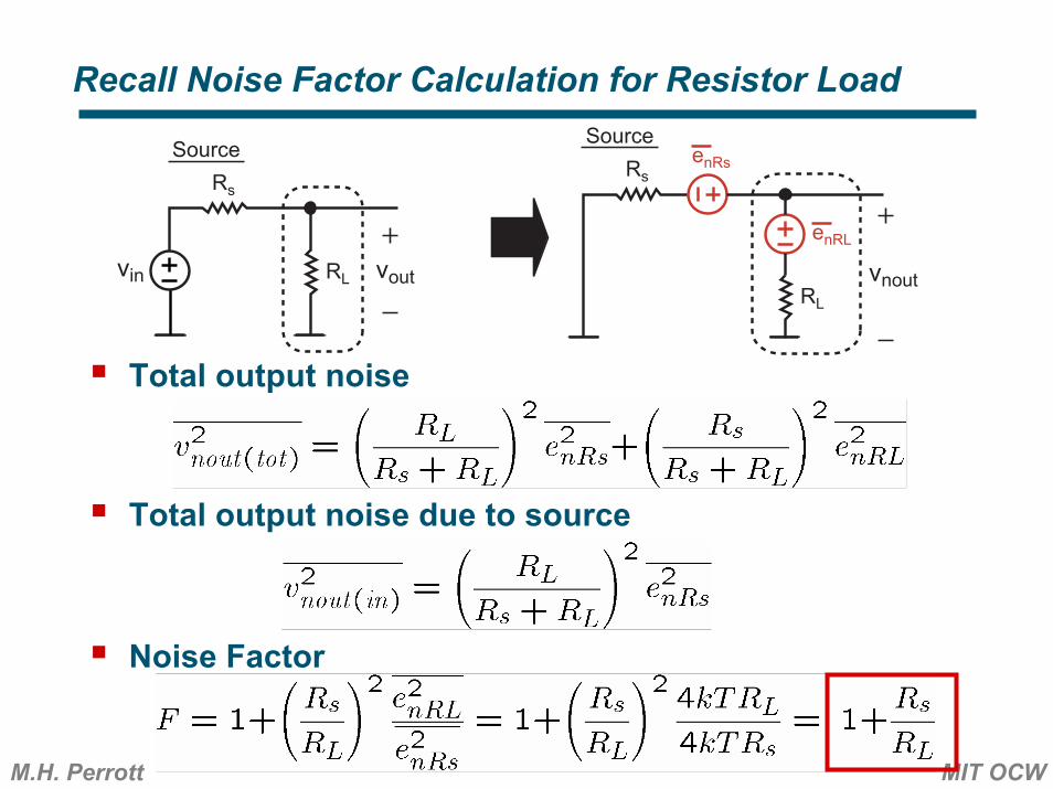
Recall Noise Factor Calculation for Resistor Load
Total output noise
Total output noise due to source
Noise Factor
vin
Rs
RL
Source
vout
enRs
enRL
Rs
RL
Source
vnout

M.H. Perrott MIT OCW
Noise Figure For Amp with Resistor in Feedback
Total output noise (assume A is large)
Total output noise due to source (assume A is large)
Noise Factor
Vin
Rs
RfSource
Vout
enRs
AVref
Rs
RfSource
VnoutA
enRf
incrementalground

M.H. Perrott MIT OCW
Input Impedance For Amp with Resistor in Feedback
Recall from Miller effect discussion that
If we choose Zin to match Rs, then
Therefore, Noise Figure lowered by being able to choose a large value for Rf since
enRsRs
RfSource
VnoutA
enRf
Zin

M.H. Perrott MIT OCW
Example – Series-Shunt Amplifier
Recall that the above amplifier was analyzed in Lecture 5Tom Lee points out that this amplifier topology is actually used in noise figure measurement systems such as the Hewlett-Packard 8970A- It is likely to be a much higher performance transistor
than a CMOS device, though
M1
Vbias
vinvout
Rf
R1
Rs
RL
Rin Rout
vx


