
Advances in display technologies
Hoi-Sing Kwok
Center for Display ResearchHong Kong University of Science and Technology
Display symposium November 2008

2
Displays – historyFirst generation – CRT
Braun tube was invented in 1897RCA patented color picture tube in 1954Still has a market of US$17B in 2007
Second generation – LCDLC effect was discovered in 1888Field effect was invented in 1968 by RCA researchersActive matrix LCD commercialized in 1990
Third generation – OLED Invented in 1982 by C W Tang (邓青云)Passive matrix display commercialized in 2000Active matrix display commercialized in 2003Large scale deployment expected in 2009

3
Display Market
As a comparison, the semiconductor market is about $250B

4
Active matrixRegardless of display technology used, the active matrix backplane is essentialPassive matrix – multiplex driving
LCD – time multiplexing reduces selection ratioLimited multiplexing to 240 lines (STN)OLED – time multiplexing increases current loadingLimited to 100 lines
Active matrix – one or more transistors per pixelIndividual voltage or current control of pixels with no crosstalk
Thin film transistors (TFT)Amorphous silicon (a-Si)Polycrystalline silicon (poly-Si)

5
Display manufacturing
Active matrix array process :
growth of TFT on glass
Backend :
deposition of OLED
or fabrication of LCD cell
Module manufacturing: driver IC, PCB, backlight in case of TFT LCD
Passive matrix : simple etching of ITO glass
PMOLEDPMLCDPassive matrix
AMOLEDAMLCDActive matrix
OLEDLCD

6
FPD technology• Display research encompasses
electronics, optics, material and vacuum technologies
• FPD has obvious advantages over other technologies in thickness, weight, and power consumption
• High-resolution, full-color and video FPD’s need active-matrix addressing
• SOP or SOG technology is required for versatile, compact and super high resolution mobile displays DisplayDisplay
Flat-Panel display
AM-FPD
SoP

7
FPD mega trend
*From Samsung Electronics
Both require LTPS

8
Thin film transistors90% of TFT fabs use a-Si technologyPoly-Si is gaining market share
HTPS – used in LCD projectorsLTPS – can be grown on glass
LTPS (low temperature poly-Si) is needed forCircuits on glass – integrated drivers and scanners and multiplexer – reduces use of external IC and connectors to panelMuch smaller TFT ⇒ larger aperture ratio – mobileapplications Much more stable than a-Si under high current loading (OLED needs current to drive)
9
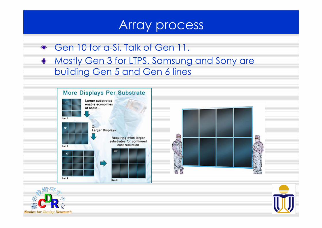
Array processGen 10 for a-Si. Talk of Gen 11.Mostly Gen 3 for LTPS. Samsung and Sony are building Gen 5 and Gen 6 lines

10
Silicon technologies

11
Comparison of a-Si, poly-Si TFT
Mobility : ~500 cm2/VsN/P-channel TFT
(CMOS)< 1 ㎛
Mobility : 50~200 cm2/Vs
N/P-channel TFT (CMOS)2~3 ㎛
Mobility : 0.5~1 cm2/Vs
N-channel TFT3~5 ㎛
System on panelPoly-Si TFTa-Si TFT
Gate Driving IC
Source PCB (Controller, converter, gamma, DC-DC)
Data Driving IC
Controller PCB(Controller, Y-source,
Amp, DC-DC)
Data Driving IC
Control IC, Peripheral circuits
Data Driving IC
Poly-Si TFT-OLED
System on Panel
a-Si TFT-LCD

12
AMOLED bottleneckAMOLED is now in the same situation as LCD in 19901990 – introduction of TFT array process – active matrix – AMLCD quickly replaced STN in notebook computersOLED lacks a TFT that can bring it to the next level -current TFT is developed for LCD Difference: LCD needs voltage driving and OLED needs current drivingPotential LTPS technologies for OLED:
MIC, SLS, CGS, GGS, MICC, MILCBG-TIGR (HKUST proprietary)

13
LTPS – external connectorsCommon practice: LTPS line scanner plus data multiplexerFor example, use 1/10 multiplexer for VGA display, then external connection is reduced from 1120 to 110Greatly improves packaging yield and cost
14
LTPS – aperture ratioLTPS TFT can be much smaller than those with a-SiFor example 3” VGA,a-Si ~50%,LTPS~80%Larger aperture ratio means smaller backlight and lower power consumptionImportant for mobile displays
15
LTPS – data processingLTPS TFT is much faster than a-Si TFTFast data loading needed for field sequential colorCan also incorporate multiple transistors on each pixel for extra functions such as sensors, touch panels

16
LTPS market2.2” QCIF - 30% LTPS2.4” QVGA - 70% LTPS3-4” VGA(cell phones, PDA) - 100% LTPSSmall palmtop - 100% LTPSIn general, the division between LTPS and a-Si TFT is 150 dpiMore and more LTPS LCD for mobile displays

17
Active matrix LCD and OLED
Scan Scan lineline
Data lineData line
AddressAddress TFTTFT
Liquid Liquid crystal crystal
cellcell(C(CLCLC))
CCss
Address TFTAddress TFT
CCss
OLEDOLED
Data lineData linePower linePower line
DriveDrive TFTTFT
LC PixelLC Pixel OLED PixelOLED Pixel

18

19
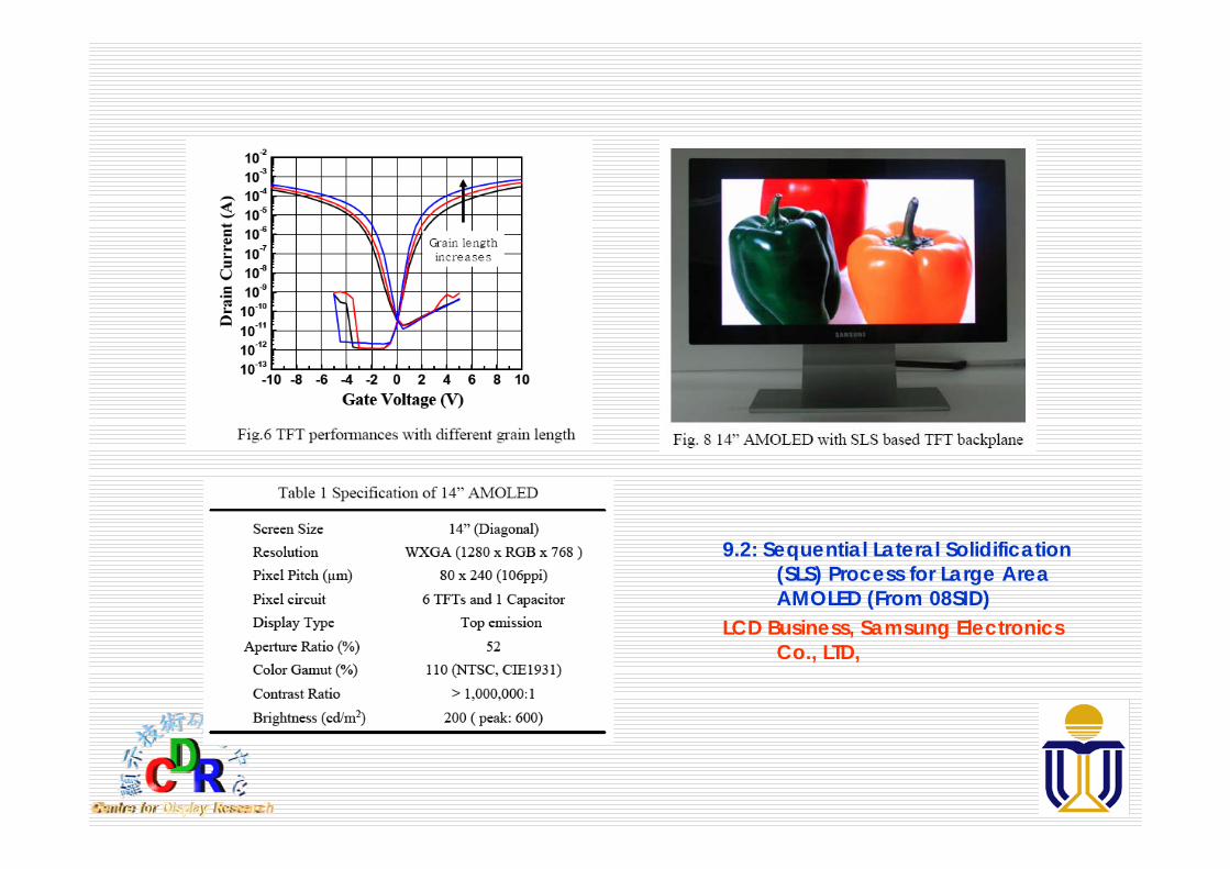
Recent results on SLS poly-Si TFT
SID 2008 9.2: Sequential Lateral Solidification (SLS) Process for Large Area AMOLEDLCD Business, Samsung Electronics Co., LTD,
6 TFT + 1 capacitor for pixel circuit
20
9.2: Sequential Lateral Solidification (SLS) Process for Large Area AMOLED (From 08SID)
LCD Business, Samsung Electronics Co., LTD,

21
Recent results on SPC TFT OLED
9.3: 15-inch AMOLED Display with SPC TFTs and symmetric drivingLG Display R&D Center, Anyang-shi, Gyeonggi-do, Korea
W/L of 6 µm/18 µm,The threshold voltage, -2 V sub-threshold swing, 0.6 V/decMobility, 30 cm2/Vs,

22
Excimer laser annealingDeveloped for LCDVariations – CGS (continuous grain silicon) of Sharp, SLS (single crystal like silicon) of SamsungProblems : too expensive and mura defects

23
Metal Induced crystallization of a-Si
Metal Induced Lateral crystallization (MILC)/Metal Induced Unilaterally crystallization (MIUC)
Disk-like domain poly-Si or giant grain (GGS) poly-Si

24
Metal induced lateral/unilaterally crystallization
Low temperature crystallization ( < 600 ℃) glass substrate applicableLarge grain size compared to SPCHigh mobility, high uniformity
Advantages
Disadvantages
High nickel concentrationin some areaAlignment misplacement caused by the shrinkage of the glass substrate during the crystallization process
Crystallization inducing holeNi
MILC
a-Si MILC MIC
High Ni Concentration at the MILC
25
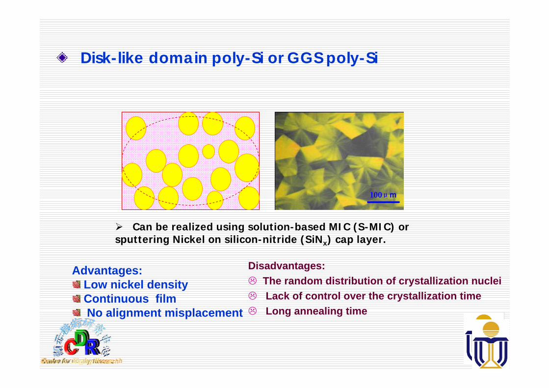
Disk-like domain poly-Si or GGS poly-Si
Can be realized using solution-based MIC (S-MIC) or sputtering Nickel on silicon-nitride (SiNx) cap layer.
Disadvantages:The random distribution of crystallization nuclei Lack of control over the crystallization time Long annealing time
Advantages:Low nickel density Continuous film No alignment misplacement

26
Defined grain (DG) Poly-Si
30µm Nickela-Si
Substrate
Silicon Oxide
Crystalline Nuclei Lines
Poly-Si
Cross section of the DG structure
Aims: Reduce nickel residualReduce crystallization timeImprove film uniformity

27
GGS and DG poly-Si
Optical microscopy images of amorphous silicon film after one hour annealing at 590℃ in N2 atmosphere employing (a) GGS technology and (b) CZD technology.
30µm 30µm
(a) (b)
GGS – spontaneous, random
DG – patterned and controlled

28
0
20
40
60
80
100
0 50 100 150 200 250Annealing time(mins)
Ave
rage
cry
stal
lizat
ion
frac
tion
(%)
CZD-PSGGS-PS
This figure shows the average crystallization fraction over large area substrate of the film employing GGS and DG technology as a function of the annealing time at 590℃. 100% crystallization fraction can be obtained using DG technology at 60 mins, while that is just about 40% of the GGS technology.

29
microscope photo of TFTW/L=30µm/10µm
500nm SiO2
500nm LTO
Schematic cross-section of a P-channel CZD poly-Si TFT
Metal Gate
S/D
poly-Si
Al-S/D electrode
Substrate
TFT structure and plan-view photos
30
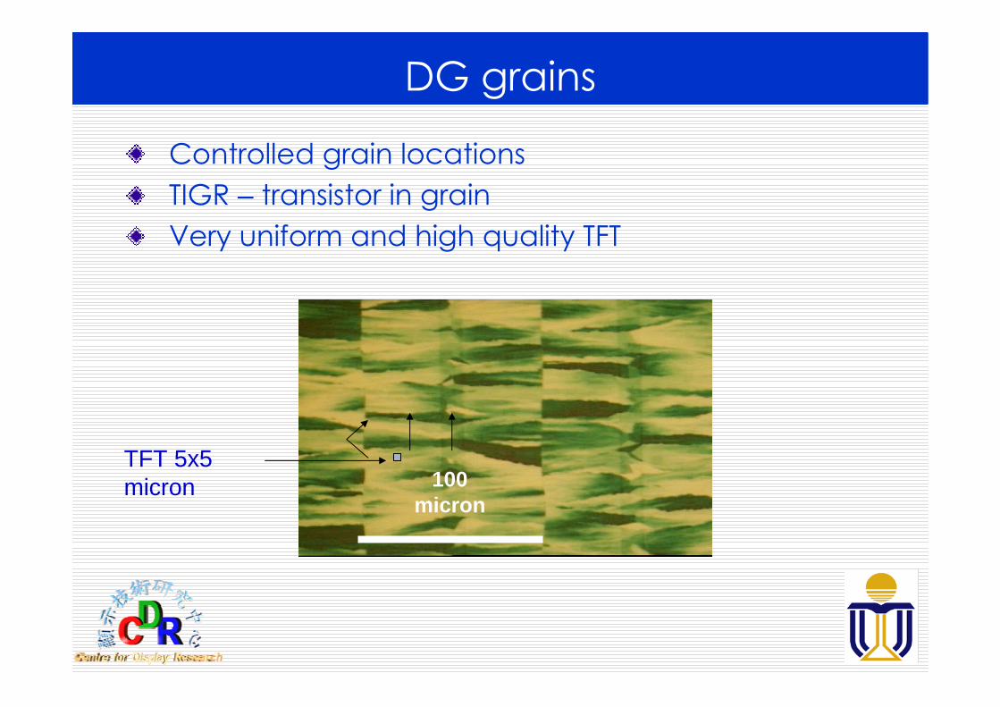
DG grains
Controlled grain locationsTIGR – transistor in grainVery uniform and high quality TFT
100 micron
TFT 5x5 micron

31
Latest invention-BG TFTBG – bridged grainHKUST patented technology

32
MIC-TFT & MIC-BG-TFT (p-channel)
1.E-12
1.E-11
1.E-10
1.E-09
1.E-08
1.E-07
1.E-06
1.E-05
1.E-04
1.E-03
1.E-02
-40 -30 -20 -10 0 10
Vgs(V)
Ids(
A) [
Vds
=-5V
]
0
20
40
60
80
100
120
140
160
180
200
µFE(
cm2 /V
s)
MIC
Active layer: 45nmW/L=30µm/10µmTox=100nmVds=-5V
B+ Implantationdosage: 4E15/cm2
MIC-BG
MIC-TFT & MIC-BG-TFT (p-channel)
33
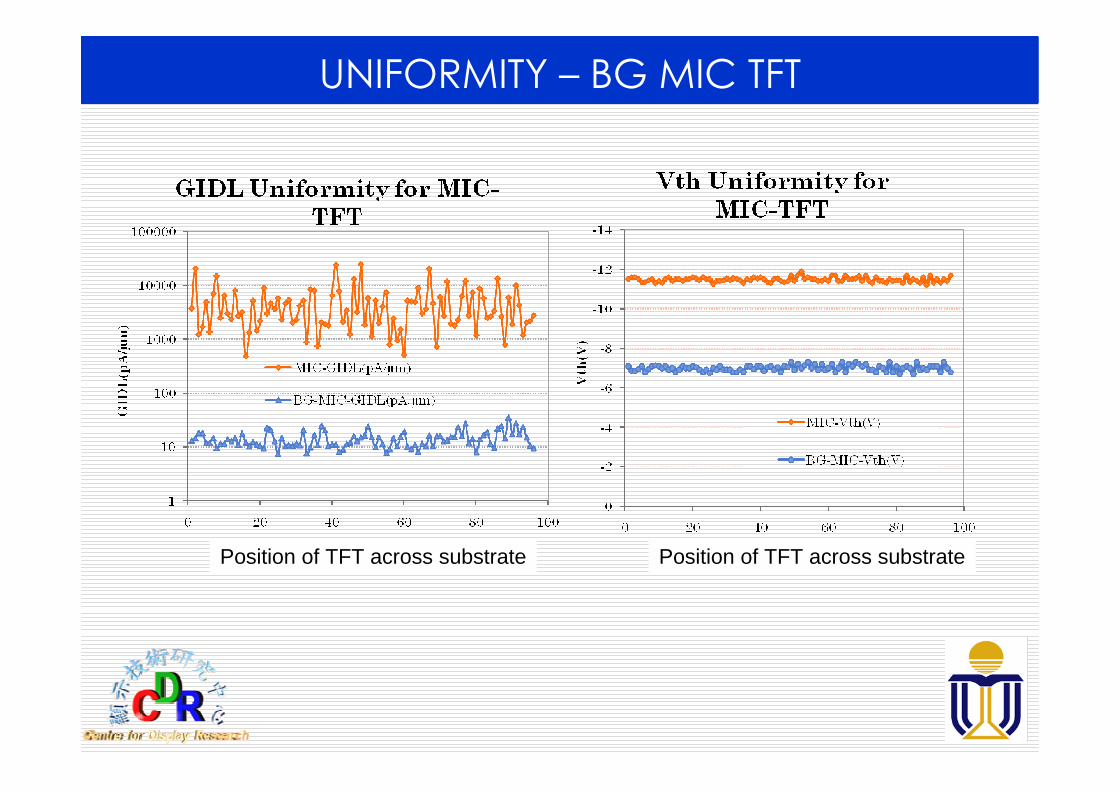
UNIFORMITY – BG MIC TFT
Position of TFT across substratePosition of TFT across substrate

34
SummaryLTPS technology is increasing in importanceHKUST BG-TIGR technology is very competitivePilot line in Foshan being constructed
35
Back to realityLCD is not exactly standing stillIt is being improved constantly – cost downWhat needs to be improved?
Energy consumption – light utilization is only 5-8%Brightness, viewing angle, speed, contrast, color saturation, cost
How can LCD be improved? Light recyclingField sequential colorLED dynamic backlight

36
Fast LCD modesOCB and NBBThin cell gap TN, VAFerroelectric FlexoelectricOthers
OCB requires a bias voltageNBB – no-bias bend mode, made possible with high pretilt angle

37
Ferroelectric LC
Already in production for LCOS Binary switching. Frame rate modulation to obtain grayscale (just like DLP)Traditional FLC are surface stabilizedNew development – V-shape monostable FLC

38
FLC based FSC display
Fujitsu SID 2000
And SID 2007

39
VA mode
J Anderson, SID 2002
40
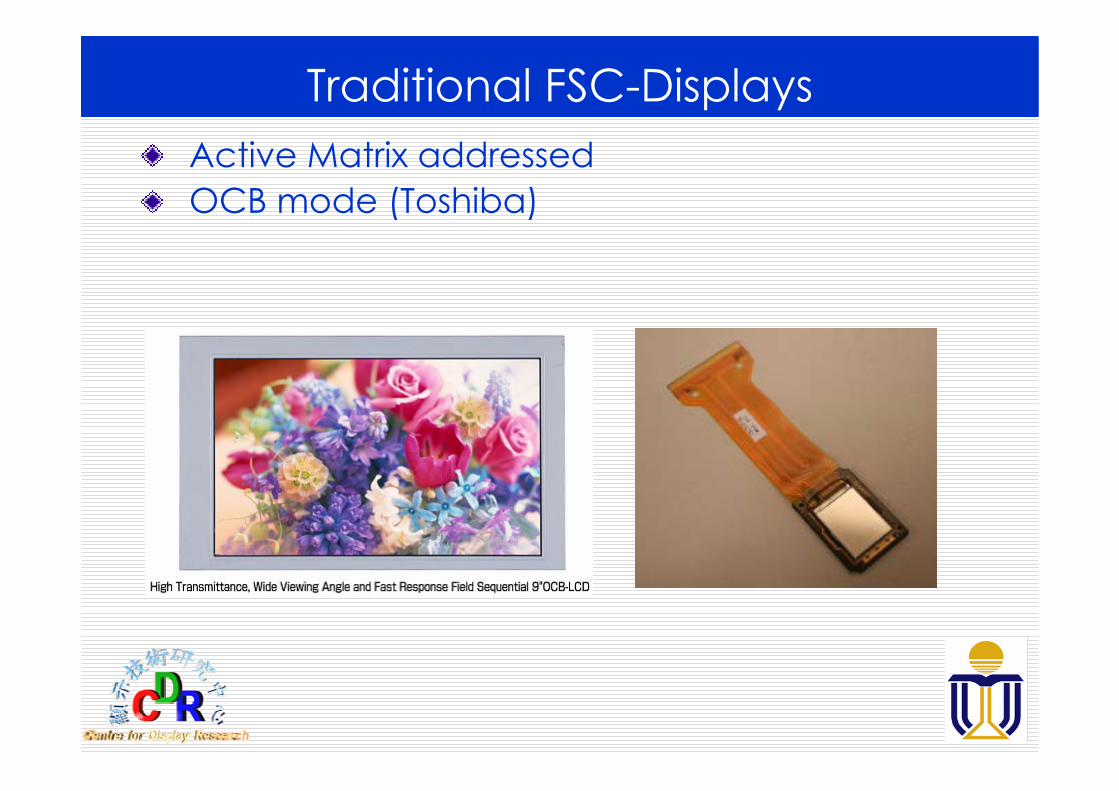
Traditional FSC-DisplaysActive Matrix addressedOCB mode (Toshiba)

41
HKUST invention – NBB modeNo bias bend modeTrue bend cell without bias voltagePossible due to a new nano-alignment layerAny pretilt angle can be obtained – impossible previously

42
Conventional pi-cell (OCB mode)
Splay Bend

43
Splay to Bend transition is tricky
TMD SID 2004
44
Critical holding voltage
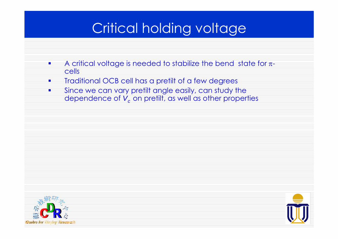
A critical voltage is needed to stabilize the bend state for π-cellsTraditional OCB cell has a pretilt of a few degreesSince we can vary pretilt angle easily, can study the dependence of Vc on pretilt, as well as other properties

45
Dependence of Vc on θο
Bend cellSplay cell

46
No-bias bend (NBB) cell If the pretilt angle is large enough, no critical holding voltage is needed.The stable configuration is the bend state, not the splay state.NBB has smaller effective birefringence and fasterswitching than OCBOptimization of NBB optical properties
47
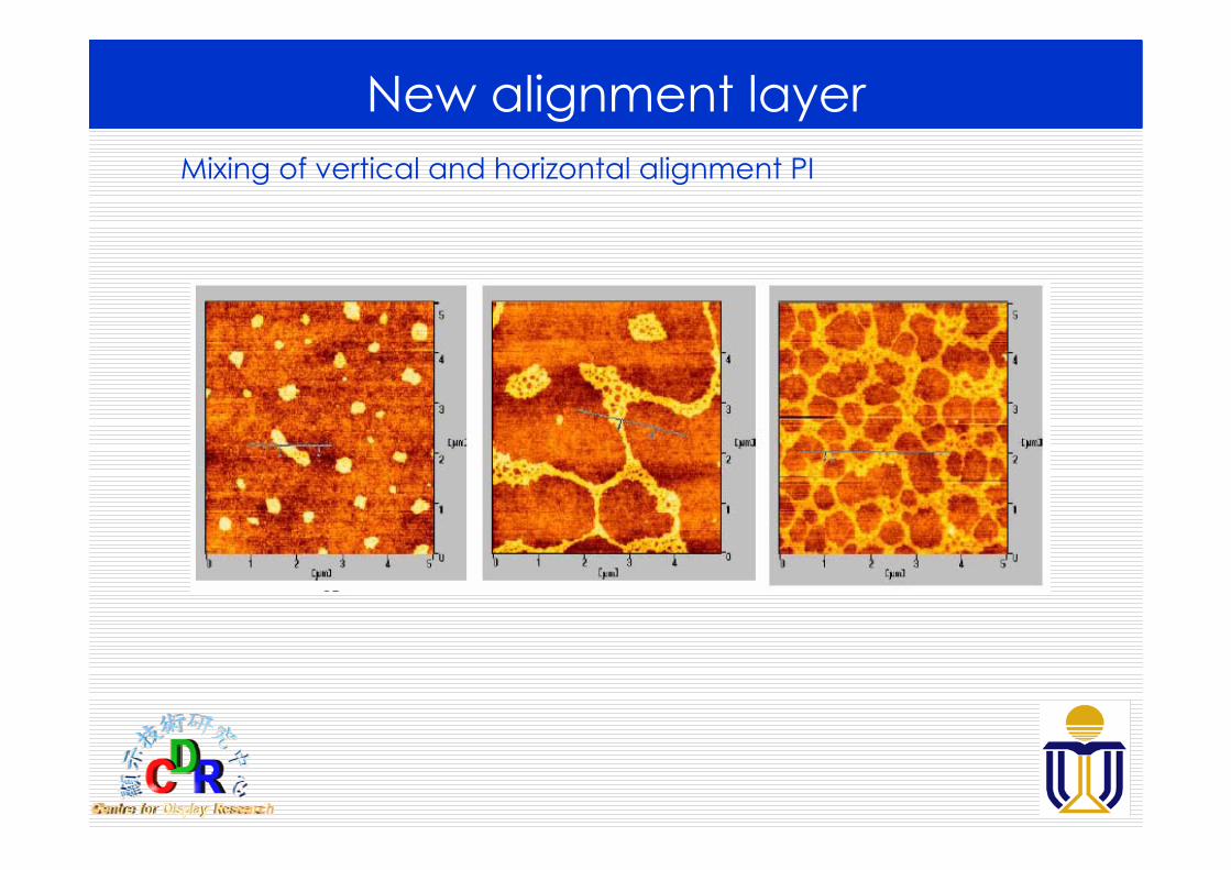
New alignment layerMixing of vertical and horizontal alignment PI

48
Surface morphology
AFM5µm
V
High resolution Microscope50µm
HV
H

49
Any pretilt angle can be obtained
0
10
20
30
40
50
60
70
80
90
0.000% 5.000% 10.000% 15.000%
Percentage of JALS2021
Pretilt angle

50
Fast response times of NBB50° pretilt angle π-cell (d = 5 µm)
Off time: 2ms On time: 70µs
1.00ms/div 50µs/div

51
Gray-to-gray switching speed of NBB cell
(µs)

52
Latest development in NBBNew Alignment method is development for large area uniform high pretilt angle generations
67ο, 52ο, 39ο, 27ο

53
Optical performance is improved By using our new alignment layers, the brightness performance of NBB is improved by 20% without any compensation film applied
Pretilt: 52 degCell gap: 5.25µm
Δn: 0.2Δε:+7
Pol/Anal=+-45degFor both Cells A, B
Α
Β
54
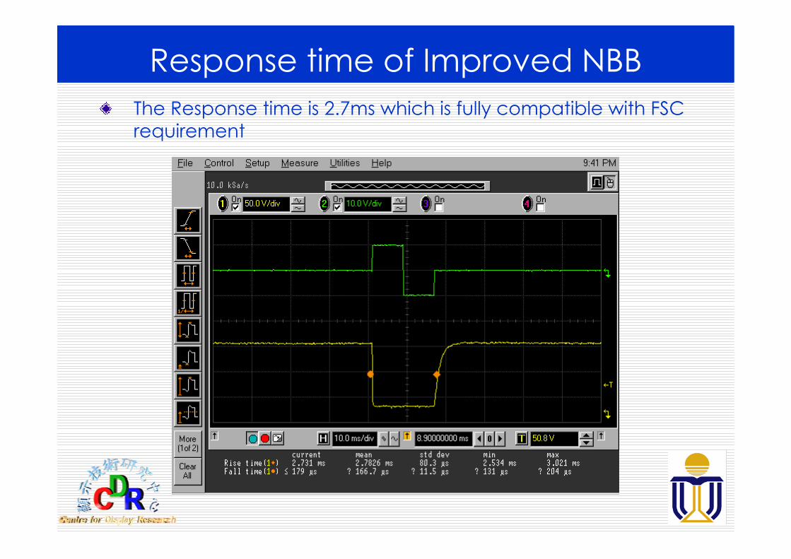
Response time of Improved NBBThe Response time is 2.7ms which is fully compatible with FSC requirement

55
SummaryImproved NBB show much better EO performance than traditional one. Further increase of ∆ε to 14 can reduce the driving value to <5V.
2.7ms2.1msResponse Time
80%60%Brightness75.327Contrast
Modified NBB
Traditional NBB

56

57
ConclusionsDisplay is in a transition to third generationCore technology – LTPS TFTMobile display will be dominated by LTPS technologiesMany LTPS technologies are near commercial successFast LCD still has a bright future, especially for large displays
58
Thank you!


