Arbeitskreis EF-EELS
Lausanne (CH) 29-30 September 2004
New developments in EELS spectrum-imaging
Christian COLLIEX

Outline
Recording 3D spectrum-imaging data cube :application to EELS spectroscopy
Definition and performance in terms of energy and spatial resolution : How to improve them?
Processing spectrum-image data cubes : quantification, deconvolution, MSA…
Applications in various fields : elementalmapping, bond mapping, ultimate sensitivity
Future issues

Ultramicroscopy 28 (1989) 252-257
Spectrum-image : the next step in EELS digital acquisition and processing
C. Jeanguillaume and C. Colliex
This paper defines a new concept in EELS digital acquisition and processing : the spectrum-image. This is a 3D array of nxnxs numbers, the first two axes of which correspond to the x-y position on the specimen as for any image, while the third is associated to a complete electron energy-loss spectrum…

Recording 3D spectrum-image data cube :
Electron Energy Loss Spectroscopy(EELS)
in a (S)TEM?
1. The PEELS/STEM approach2. The EFTEM approach
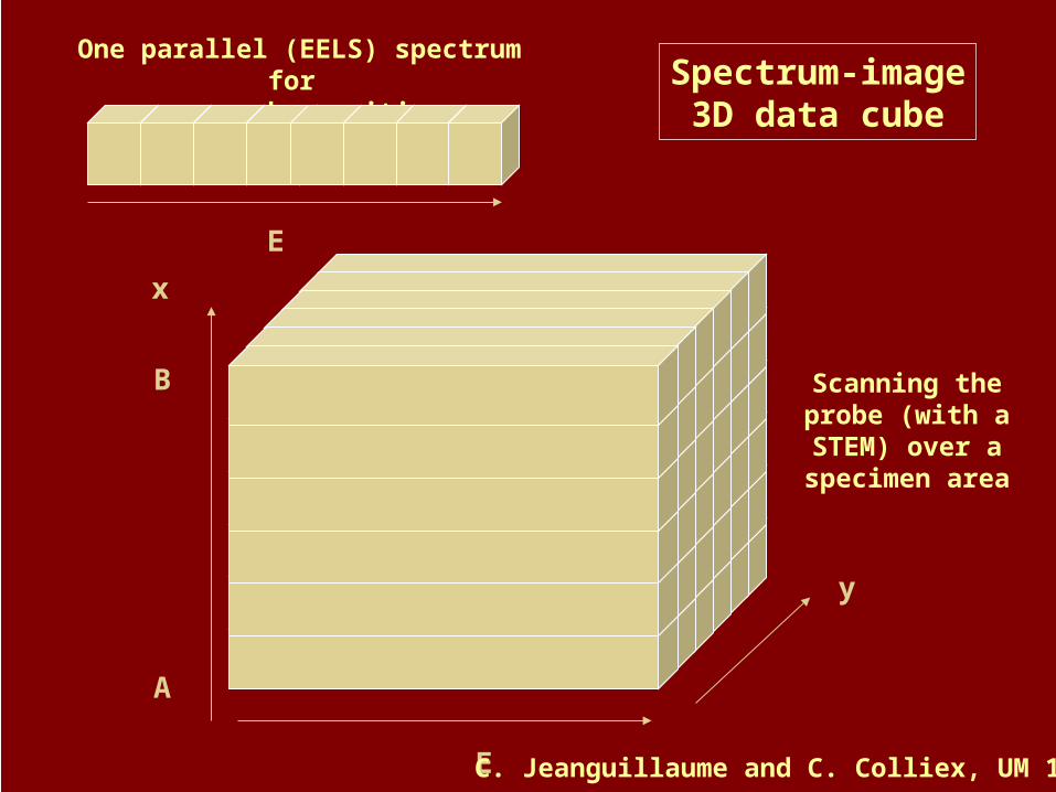
Spectrum-image3D data cube
One parallel (EELS) spectrum for one probe position
A
B Scanning the probe (with a STEM) over a
specimen area
y
x
E
E
C. Jeanguillaume and C. Colliex, UM 1989

I I I I
250 300 350 400
0-
40-
(nm)
Energy Loss (eV)
SPECTRE LIGNE
A
B
SPECTRUM LINE
HADF image
20 nm
450400350300Energy Loss (eV)
EELS spectrum
AB
Specimen
Magnetic spectrometer
Field emission gun
E
E -E
o
o
CameraCCD
HADF detectors
Spectrum
Probe• 0.1 to 1nA• in 0.5 to 1 nm
Scanning coils
The spectrum imaging mode (in Orsay)
100 keV
0.5 to 0.8 eV1 ms to 5 s

0
1000
2000
3000
4000
5000
6000
7000
0 20 40 60 80
Cu-Co multilayers
HADF Cu map
Co map
40 nm
Maps extracted from a spectrum-image data set : .) 256x256 pixels .) 10 ms/pixel .) total energy window from 600 to 1100 eV with 0.5 eV/channel .) edges of interest : Co L23 at 780 eV Cu L23 at 930 eV
.) energy window for signal integration : 120 eV

Reading as a sequence of energy filtered images, an EELS 3D data cube acquired as a collection of individual spectra (64x64 of 1400 channels) :
Probe size and pixel step = 0.75 nmEnergy loss channel = 500 meV
Acquisition time per spectrum = 100 ms
M. Walls, M. Tencé, C. Duhamel, Y. Champion, EMC 12 Antwerp

Image spectrum
x
E
y
E1 E2
One energy filtered image at energy loss E
Pile up of energy filtered images from E1 to E2
E
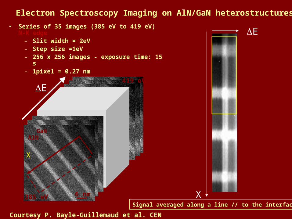
385 eV
419 eV
6 nm
AlNGaN
• Series of 35 images (385 eV to 419 eV) N-K edge
– Slit width = 2eV– Step size =1eV– 256 x 256 images - exposure time: 15 s– 1pixel = 0.27 nm
E
X
X
Electron Spectroscopy Imaging on AlN/GaN heterostructures
Signal averaged along a line // to the interface
Courtesy P. Bayle-Guillemaud et al. CEN Grenoble

Extraction of the local spectra : N-K in AlN and GaN layers
385 390 395 400 405 410 415 420
AlN-ESI
AlN-buffer
Energy Loss (eV)
385 390 395 400 405 410 415 420
GaN-ESI
GaN-buffer
Energy Loss (eV)

Extraction of spectra at the interface AlN
GaN
- 1 spectrum every 0.27 nm- Spatial resolution estimated around 0.5 nm

What about EELS energy and space resolution ?
A survey of new tools developed for improving them

∆x
∆y
∆E
An elementary unit volume in the 3D data cube
PEELS/STEM : ∆E defined by spectral energy resolution∆x, and ∆y defined by probe size
EFTEM : ∆E defined by width of energy slit∆x and ∆y defined by spatial resolution in energy filtered image (major component is the Cc blurring term)

In the years 1967 to 1970, a Castaing and Henry
type filter is built into an Hitachi HU 11B column (Colliex and Jouffrey)
Before the digital era

Energy resolution in EELS spectra
Digitizing a C graphite K-edge micrograph recorded with the
Castaing and Henry filter (C. Colliex Ph. D. 1970) Microdensitometer profile (1970)
Scanner + Digital Micrograph (2002)
Energy resolution : 1 to 1.5 eV

Spatial resolution in energy filtered images
A to E : Energy filtered images recorded respectively with the zero-loss, the plasmon-loss, energy windows before, on top and after the carbon K-edge.
F : micrograph of the carbon K-edge with the two narrow lines for the * and the * edges
From Colliex, Ph.D. thesis, Orsay (1970)
Spatial resolution : a few nm

1
1
0.2
0.2
2
2
∆x (nm)
0.1 0.1
0.3 0.3
1 1
∆E
(eV
)
EFTEM70s
Tanaka with monochromator
80s
Orsay STEM90s
1
3
2
Where are we going ?1) in imaging
2) in spectroscopy3) in spectrum-imaging
IBM STEM90s

Advances in imaging :Correction of aberrations
(i) of the probe forming lens: ultra-small probes and HAADF contrast
(ii) of the imaging lens:UHRTEM and quantitative measurements

Improving spatial resolution in a STEM with a probe-forming Cs corrector
2nd generation Nion Cs corrector in a VG STEM Key features• fits into existing high performance STEM• second generation quad/oct Cs corrector• optimized EELS coupling
Advantages• corrector replaces scan coils - height of scope stays same• <1 Å probe size at 100 kV• 200 pA of current in a 1.4 Å probe
Result (courtesy Dr. A.R. Lupini, ORNL, may 2002)
Bi single atom dopants in Si
1 nm
C1virtual obj. ap.
dark field detector 1
C2
scan, align, stigmator
Cs corrector(4Q+3O)
TV
quadrupole/octupole EELS coupling
module
dark field detector 2
EELS
alignment
sample
objective lens
obj. ap.
gunNionVG


Advances in spectroscopy :
Monochromators

The Monochromated Tecnai F20 solution
Monochromator on
1.0 Å
20 nm20 nm
• Looks like a standard Tecnai
• Has all standard specifications when monochromator is off
• Has 0.1 eV resolution at < 2nm spatial resolution in STEM when monochromator is on
EELS HR-TEM
180
200
220
0 10 20 30 40 50 60 70 80nm
STEMBand gap

Zero-loss peak energy distribution : a comparison
courtesy F. Hofer and K. Kimoto

Comparison of Co L23 lines in CoO
courtesy F. Hofer, Graz

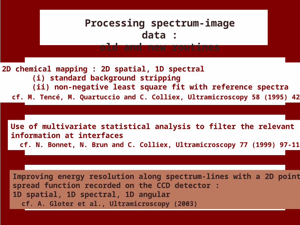
Processing spectrum-image data :old and new routines
2D chemical mapping : 2D spatial, 1D spectral(i) standard background stripping(ii) non-negative least square fit with reference spectra
cf. M. Tencé, M. Quartuccio and C. Colliex, Ultramicroscopy 58 (1995) 42-54
Use of multivariate statistical analysis to filter the relevant information at interfaces cf. N. Bonnet, N. Brun and C. Colliex, Ultramicroscopy 77 (1999) 97-112
Improving energy resolution along spectrum-lines with a 2D point spread function recorded on the CCD detector : 1D spatial, 1D spectral, 1D angular cf. A. Gloter et al., Ultramicroscopy (2003)

Chemical mapping in complex situations (BN nanotubes and
nanoparticles)
Elemental MappingHADF
Bore
B K
Carbon
C K
Calcium
Ca L
Azote
N K
Oxygen
O K

20 nm
Beyond elemental mapping : mapping bonding states
180 200 220 240 260Energy loss (eV)
Inte
nsity
180 190 200 210Energy loss (eV)
Inte
nsity
BK
Reconstructed spectrum
Exp.
180 190 200 210
Energy Loss (eV)
220
BKBN
B2O3
metallic B
ReferencesNNLS Fit
4
4
1
1
2
2
5
5
3
3

B2O3
BN
Amorphous B
NNLSBN
B2O3
Amorphous B
Reconstructed images from B K edges
Metal/oxyde particles on a BN nanotubes network
Bam. @ BN @ B2O3 multishell nanoparticle
10 nm
10 nm
10 nm
20 nm
20 nm
20 nm

10 nm
1) centre
(b)
BN reference spectra
110 120 130 140 150 160 170
Energy Loss (eV)
*
*
With spectrum imaging mode :Chemical, Bonding and Orientation maps are accessible
B metal
B oxyde
BN centre
BN edge
q
ko
Momentumtransfer q
c axis ko
2) edge
2) edge
1) centreOne step further, NNLS fit usingbonding and orientation changes
of fine structures on B-K edge
A. Vlandas (LPS)R. Arenal de la Concha (ONERA)

Processing spectrum-image data :old and new routines
2D chemical mapping : 2D spatial, 1D spectral(i) standard background stripping(ii) non-negative least square fit with reference spectra
cf. M. Tencé, M. Quartuccio and C. Colliex, Ultramicroscopy 58 (1995) 42-54
Use of multivariate statistical analysis to filter the relevant information at interfaces cf. N. Bonnet, N. Brun and C. Colliex, Ultramicroscopy 77 (1999) 97-112
Improving energy resolution along spectrum-lines with a 2D point spread function recorded on the CCD detector : 1D spatial, 1D spectral, 1D angular cf. A. Gloter et al., Ultramicroscopy (2003)

LSMO/STO/LSMOinterface
LS
MO
STO
LS
MO
ELNES results - O-1s edge
In LSMO, the first structure “a” is attributed to overlapping bands
of Mn-3d character
a
O-1s edge seems to vary continuously from the LSMO
to the STO phase
As in Mn-2p, no trend towards Mn 4+ and Sr enrichment is detected at the interfaces

LSMO/STO
0
5
10
15
20
0 5 10 15 20 25 30 35 40 45 50axis number
O-1saxis 1
axis 2
axis 3
spectrum coordonates
MULTIVARIATE STATISTICAL ANALYSIS (MSA)
ELNES results - O-1s edgeDecomposition and reconstruction of the spectrum-image
(i) powerful tool when used in association with the spectrum-image
technique, involving 64 to 512 spectra in the 1D mode and 103 up to
a few 104 spectra in the 2D mode
MSA analyses the variance and the covariance of a multidimensional data set (energy and space axis)
Selection of the different information contributing to the overall signal
It also reduces the identified noise (thresholding method) and assists in detecting and locating the different
ELNES structures (quantification under certain conditions)

LSMO/STO/LSMOinterface
Multivariate Statistical Analysis (MSA)of the O 1s spectrum-line data set
MSA analyses the variance and the covariance of a
multidimensional data set built from each energy
channel and probe location
Image 1 corresponds to the reconstruction of the signal using the two first components : reveals only the spatial location of the LSMO and STO layers. axis 3
2
Image 2 corresponds to the following component. No new significant information is clearly located at the interfaces.
a
axis1+axis2
Energy loss (eV)
Probe position
(nm)
LSMO
STO
LSMO
531 545
1
It confirms that any spectrum in the data set can be built as a
linear combination of the LSMO and STO reference
spectra
Processing spectrum-image data :old and new routines
2D chemical mapping : 2D spatial, 1D spectral(i) standard background stripping(ii) non-negative least square fit with reference spectra
cf. M. Tencé, M. Quartuccio and C. Colliex, Ultramicroscopy 58 (1995) 42-54
Use of multivariate statistical analysis to filter the relevant information at interfaces cf. N. Bonnet, N. Brun and C. Colliex, Ultramicroscopy 77 (1999) 97-112
Improving energy resolution along spectrum-lines with a 2D point spread function recorded on the CCD detector : 1D spatial, 1D spectral, 1D angular cf. A. Gloter et al., Ultramicroscopy (2003)

Image deconvolution
Image equation A x + n = bwe want an estimation of x the unblurred objet
• Iterative RL converges to the maximum likelihood solution for Poisson statistics in the data.• It conserves flux both globally and locally at each iteration.• The restored images are robust against small errors in the used point spread function.
we knowA the point spread function b the measured blurred imagewith unfortunately an additive noise n
• Application to EELS spectrum acquired with 2D CCD detector• Matrix A should take into account : CCD-PSF, spectrometer aberration,
energy width of the incident beam.
Iterative Richardson-Lucy algorithm gives an estimation x(k) of the true image x
Inverse problem

Energy deconvolution of spatially resolved EELS spectra on a VG STEM at 100kV with cold FEG :
B-K edge on an individual BN nanotube
180190200210Energy Loss (eV)0.68 eVraw dataB-K 180190200210Energy Loss (eV)0.36 eVB-Krestored data

Fe L23 and O K edges in different iron oxides
before and after RL deconvolution
705 710 715 720 725 730Energy Loss (eV)
Fe L2,3
(a)
(b)
(c)
525 530 535 540 545 550Energy Loss (eV)
x 5
O-K
(a)
(b)
(c)
A BC
D
525 530 535 540 545 550Energy Loss (eV)
O-K A B C
D
705 710 715 720 725 730Energy Loss (eV)
Fe L2,3
(a)
(b)
(c)
(a)
(b)
(c)
(a) hematite, (b) magnetite, (c) siderite

Iron Fe L2,3 edges for -Fe2O 3 hematite
705710715720725730Energy Loss (eV)
LaB6 Topcon microscope Experimental EELS after 30
iterations of RL deconvolution procedure
Fe L2,3
Atomic multiplet calculation for Fe3+ ions and an Oh crystal field
of 2 eV strength.Energy resolution of Gaussian
0.3eV has been simulated.

630 635 640 645 650 655Energy Loss (eV)
EELS Mn L2,3
How to reduce the noise.How to reduce the noise.
Richardson-Lucy and a entropy stabilisation termRichardson-Lucy and a entropy stabilisation term Mn L2,3 edges of siderite mineral Fe0.80Mn0.13Mg0.06Ca0.01CO3
635 640 645 650 655 660635 640 645 650 655 660
theoretical Mn L2,3valency 2+ , HSCrystal Field Multiplet
Energy Loss (eV)
See A. Isambert et al. JGR (2003).
Deconvolution +Multiplet calculations
Mn impurities are only divalent in this material
Energy deconvolution :2D RL procedure + Shannon Entropy stabilisation.
630 635 640 645 650 655
Energy Loss (eV)
EELS Mn L2,3
LaB6 gun !!!

705710715720725730Energy Loss (eV)TimeFe L2,3
Raw dataAcq. Time 10s/spectrum
705710715720725730Energy Loss (eV)TimeFe L2,3
After RL restoration10 iterations.
How to reduce the noise.Iron reduction of hematite sample under the illumination of a
fixed STEM-VG probe
705710715720725730Energy Loss (eV)TimeFe L2,3
Multivariate Statistical Analysis :denoising with 6 eigenvalues.
Denoising after RL is perilous since amplified noise is colored.MSA is OK but many denoising algorithms may failed.
Chrono-spectroscopy + RL deconvolution + MSA denoising

How to reduce the noise.How to reduce the noise.
We will soon used deconvolution technique stabilized with wavelets We will soon used deconvolution technique stabilized with wavelets filtering.filtering.To be fully operent in EELS, we have to build a plug-in wavelet in To be fully operent in EELS, we have to build a plug-in wavelet in Digital Micrograph (test on Matlab but everything has to be Digital Micrograph (test on Matlab but everything has to be trabsferred to « easy to use » software)trabsferred to « easy to use » software)
At the moment,At the moment,Demoising of Demoising of spectrum is OK in spectrum is OK in DM (DM (C. Charles et al. C. Charles et al. Computational Statistic Computational Statistic and Data Analysis, 43, and Data Analysis, 43,
20032003))
See example for See example for the Ca L2.3 edge.the Ca L2.3 edge.
Stabilization of Stabilization of inverse problem inverse problem algorythm on the algorythm on the road.....(J.L. road.....(J.L. Starck theory)Starck theory)

EMC 2004, Antwerp

Applications in various fields :
elemental mapping, bond mapping, ultimate sensitivity
&
Future issues

190
195200
205Energy Loss (eV)
nm
190 200 210 220Energy Loss (eV)
510
15
Probe position (nm)
B-K“surface”
tube wall
center
Boron K-edge evolution across a single BN nanotube

Surface plasmon modes on individual BN nanotubes(grazing incidence, LL () = C. Im () ~ 2)courtesy R Arenal de la Concha, coll. LPS/ONERAto be published

3nm
Peapods :
Gd@C82@SWCNT
Element selective single-atom imaging
A : HREM image
B : Schematic presentation
C : Superposed maps of the Gd N45 and C K signals extracted from a 32x128 pixels spectrum-image
See Suenaga K., M Tence, C. Colliex et al. Science 290 (2000) 2281
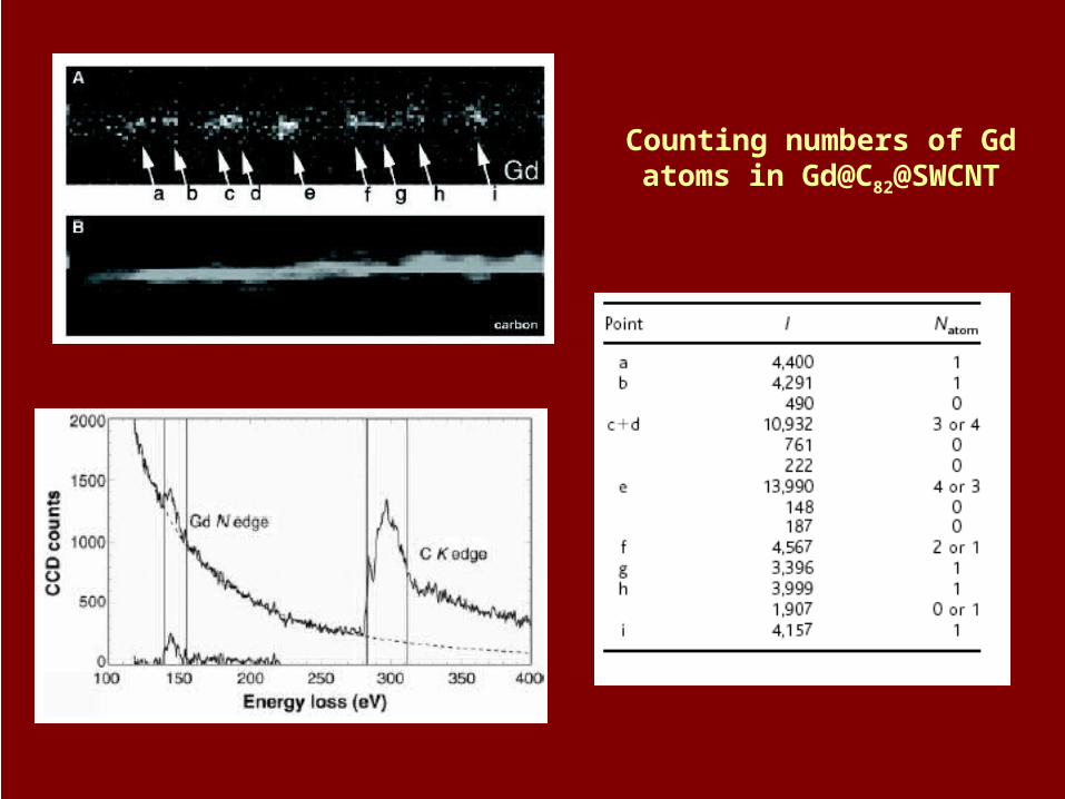
Counting numbers of Gd atoms in Gd@C82@SWCNT


Towards atomic resolution EELS
Sequence of oxygen K edge EELS spectra recorded point by point at the circled positionsacross an ultra-thin gate in a gate stack made visible in the HADF imaging mode. Thebackground corrected O K edges are displayed on the right part of the picture and they exhibita change of shape between those recorded close to the interfaces and those at the center of thedielectric film. The width of both SiO2 and sub-oxide layers has been determined after fittingany spectrum in the sequence as a linear combination of the two representative profiles. It hasshown that the two interfacial signals do not overlap only for gate oxides thicker than about1.5nm (courtesy of Muller et al [Nature 399 (1999) 758])
Representation of instrumentation typically available at different years (see dashed squaresoriginating from the upper left corner of the figure) compared with physical properties thatcan be addressed (adapted from Batson). The major progress in instrumentation occurred overthe past five years, have pushed the spatial resolution limit to about 0.1 nm (aberrationcorrectors) and the energy resolution towards 0.1 eV (monochromators or /anddeconvolution). The new projects under development are sketched with the arrows originatingfrom the presently piece of equipment now running at Orsay and at IBM. The differencesbetween the bonding mapping and the electronic structure areas are rather subjective.
The trends in instrumental upgrading

Acknowledgements are due to :
Paul Ballongue, Danièle Bouchet, Chris Ewels, Abdel Douiri , Alexandre
Gloter, Dominique Imhoff, Mathieu Kociak,
Claudie Mory, Lolwa Samet, Odile StéphanKazutomo Suenaga, Marcel Tencé Dario Taverna, Susana Trasobares,
Alexis Vlandas, Alberto Zobelli from LPS Orsay, France
Support from CNRS, EC and JST is greatly acknowledged


