
BTC’s – Packages We Love ToHate
Dale LeePlexus Corporation
Heartland SMTA Chapter Meeting12 May 2015
Dale LeePlexus Corporation

Early BTC’s
PGA - Pin Grid Array
BGA - Ball Grid Array
BGA – Bump Grid Array
PGA - Pin Grid Array
BGA - Ball Grid Array
BGA – Bump Grid Array
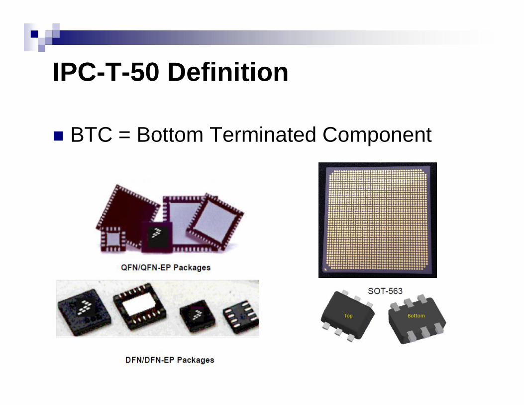
IPC-T-50 Definition
BTC = Bottom Terminated Component
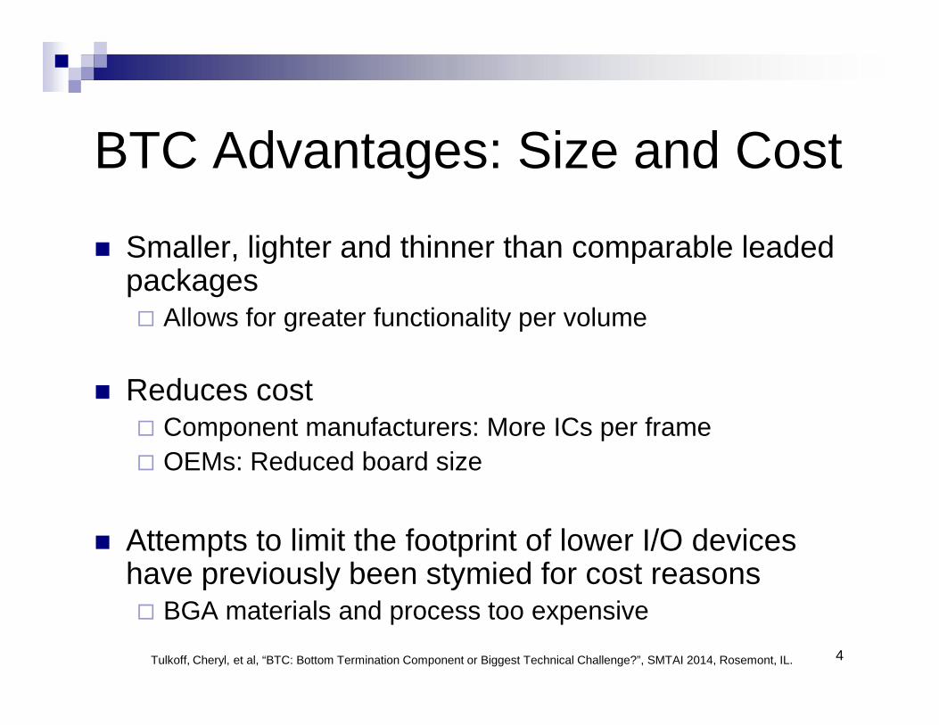
BTC Advantages: Size and Cost
Smaller, lighter and thinner than comparable leadedpackages Allows for greater functionality per volume
Reduces cost Component manufacturers: More ICs per frame OEMs: Reduced board size
Attempts to limit the footprint of lower I/O deviceshave previously been stymied for cost reasons BGA materials and process too expensive
4Tulkoff, Cheryl, et al, “BTC: Bottom Termination Component or Biggest Technical Challenge?”, SMTAI 2014, Rosemont, IL.

BTC Packaging
BTC’s Cover A Wide RangeOf Component PackageStyles And Types IncludingLeadless Chip Carriers, DFN,QFN, LGA, Flat LeadTerminated Packages (i.e.-563),Etc.
BTC’s Cover A Wide RangeOf Component PackageStyles And Types IncludingLeadless Chip Carriers, DFN,QFN, LGA, Flat LeadTerminated Packages (i.e.-563),Etc.

BTC Packaging Issue
Lack Of PackageStandardization IncreasesInconsistency In AssemblyProcesses And Stencil ToolingDesigns
Lack Of PackageStandardization IncreasesInconsistency In AssemblyProcesses And Stencil ToolingDesigns

QFN/DFN Solder Fillet Formation QFN Wetting On Edge Leads With A Solder
Bump Formed On The Pads In The Front Of TheVertical Lead Due To Non-Wetting. Determined That The Bottom Pads Are Tin Plated
Whereas The Sides (Vertical Surfaces) Are RawCopper And Not Meant To Be Soldered.
QFN Wetting On Edge Leads With A SolderBump Formed On The Pads In The Front Of TheVertical Lead Due To Non-Wetting. Determined That The Bottom Pads Are Tin Plated
Whereas The Sides (Vertical Surfaces) Are RawCopper And Not Meant To Be Soldered.

Not All Pads Are Equal
Packages That Are SingulatedBy Saw Or Punch Cut Are NotSolderable Per IPC-A-610Section 8.3.13 Notes 2 And 5
Reference: QFN/DFN Inspection of Solder Joints, Linear Technology Application Note
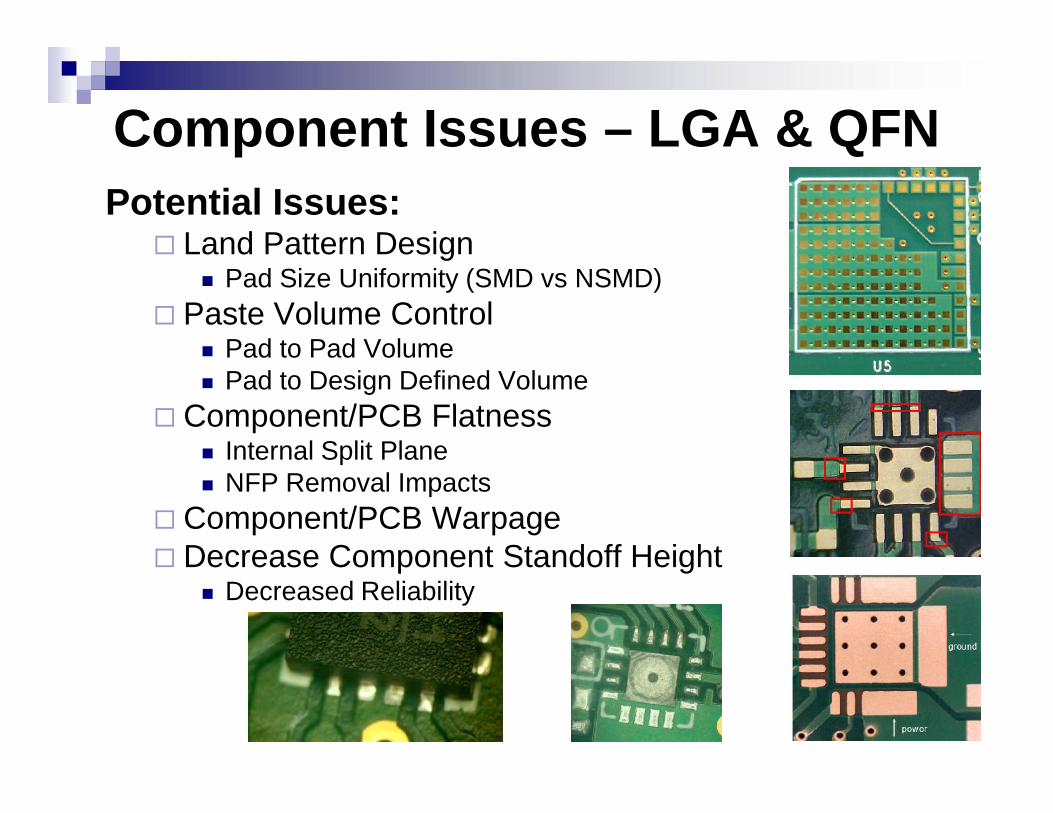
Component Issues – LGA & QFNPotential Issues: Land Pattern Design
Pad Size Uniformity (SMD vs NSMD) Paste Volume Control
Pad to Pad Volume Pad to Design Defined Volume
Component/PCB Flatness Internal Split Plane NFP Removal Impacts
Component/PCB Warpage Decrease Component Standoff Height
Decreased Reliability
Potential Issues: Land Pattern Design
Pad Size Uniformity (SMD vs NSMD) Paste Volume Control
Pad to Pad Volume Pad to Design Defined Volume
Component/PCB Flatness Internal Split Plane NFP Removal Impacts
Component/PCB Warpage Decrease Component Standoff Height
Decreased Reliability
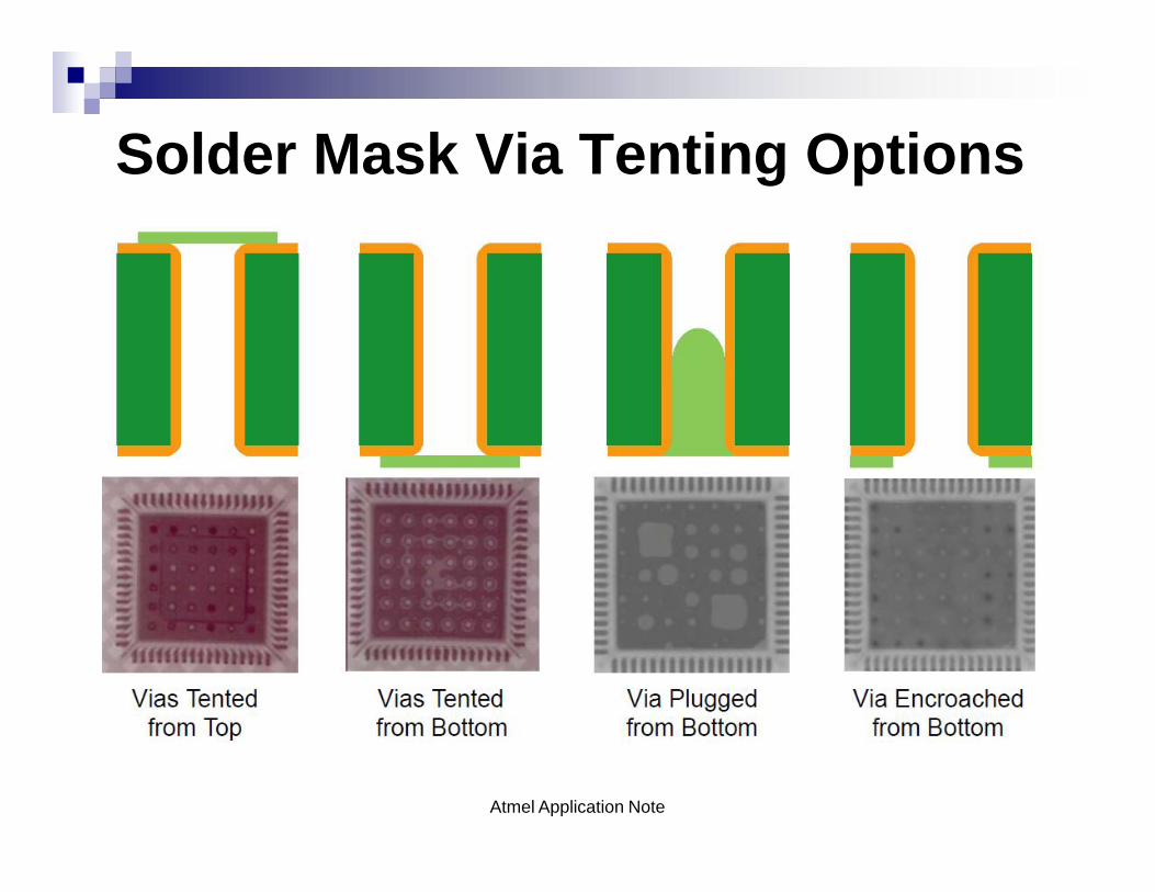
Solder Mask Via Tenting Options
Atmel Application Note

Solder Mask Design Exposed Via In Pad
Ensure Solder Mask Is NotApplied On Opposite Side OfPCB.
If Applied, Ensure Via Hole IsSmall Enough To Restrict SolderMask Flow Through To SolderAttach Side Of PCB
If Top Side Via Plugging IsRequired, Especially Is UnderBTC Components, A NoteShould Be Added To FabricationAnd Assembly DrawingReferencing This Condition
Exposed Via In Pad Ensure Solder Mask Is Not
Applied On Opposite Side OfPCB.
If Applied, Ensure Via Hole IsSmall Enough To Restrict SolderMask Flow Through To SolderAttach Side Of PCB
If Top Side Via Plugging IsRequired, Especially Is UnderBTC Components, A NoteShould Be Added To FabricationAnd Assembly DrawingReferencing This Condition

LGA Pad Design
Solder Mask Defined Non-solder Mask Defined
Pad Geometry Influences Standoff Height - Solder Wicking AroundNSMD Pads Produce Significantly Lower Molten Solder Height.
Solder Mask Defined Pads Should Be Used For LGA And 0.4mm& Smaller Pitch BGA/CSP Packages.
Solder Mask Defined Non-solder Mask Defined
Pad Geometry Influences Standoff Height - Solder Wicking AroundNSMD Pads Produce Significantly Lower Molten Solder Height.
Solder Mask Defined Pads Should Be Used For LGA And 0.4mm& Smaller Pitch BGA/CSP Packages.

LGA/QFN Package Assembly Trace Routing Under Component
Create Localized Height Variations Standoff Height Variation
Leadless Devices Are MoreSensitive To PCB/ComponentFlatness/Warpage Received Condition In-process Condition (During
Reflow/Rework Solder Process)
LGA Package
BGA Package
Trace Routing Under ComponentCreate Localized Height Variations Standoff Height Variation
Leadless Devices Are MoreSensitive To PCB/ComponentFlatness/Warpage Received Condition In-process Condition (During
Reflow/Rework Solder Process)
LGA Package
BGA Package

Board WarpageBoard Warpage Within IPC Assembly WorkmanshipStandards (0.75% May Not Be Adequate For SomeComponent Packages To Obtain High Assembly Yields
14

Removal Of Copper Plane AndUnused Pads
Removal Of CopperPlanes And Unused PadsConcentrated In ALocalized Area CanResult In Changes In PCBThickness (Flatness).These Changes UnderComponents With LimitedCoplanarity CompatibilityCan Result In OpenSolder Connections.
Removal Of CopperPlanes And Unused PadsConcentrated In ALocalized Area CanResult In Changes In PCBThickness (Flatness).These Changes UnderComponents With LimitedCoplanarity CompatibilityCan Result In OpenSolder Connections.
15

Impacts of Via Design onAssembly
Placement AndTypes Of Vias InPad Can AffectAssembly SolderJoint FormationMore Of An Impact
On SmallerComponentsAnd/Or LowerI/O Count
Placement AndTypes Of Vias InPad Can AffectAssembly SolderJoint FormationMore Of An Impact
On SmallerComponentsAnd/Or LowerI/O Count
Design and Construction Affects on PWB Reliability, Paul Reid, IPC Apex Proceedings 2012.

Stacked Via Holes
Placement Of StackedVias Under DevicesMay Create SlightMounting Pad HeightDifferencesMore Of An Impact On
Smaller And/Or Lower I/OCount or Leadless (NoSolder Ball/ SolderBump) ComponentPackages
Placement Of StackedVias Under DevicesMay Create SlightMounting Pad HeightDifferencesMore Of An Impact On
Smaller And/Or Lower I/OCount or Leadless (NoSolder Ball/ SolderBump) ComponentPackages

Solder Paste Printing Volume
Leadless Device UsageIncrease (DFN, QFN, LCCLGA) & Ultra-fine PitchComponents Impacts:
• Tighter Tolerance On SolderPaste Volume – Thinner Stencil
• Increased Uniformity Of PasteVolume Across Component(Pad to Pad)
• Paste Volume/Pad TraceEgress Direction Impact– Some Package Types Are More
Sensitive Than Others Open/Unwetted LGA Solder Connection
Leadless Device UsageIncrease (DFN, QFN, LCCLGA) & Ultra-fine PitchComponents Impacts:
• Tighter Tolerance On SolderPaste Volume – Thinner Stencil
• Increased Uniformity Of PasteVolume Across Component(Pad to Pad)
• Paste Volume/Pad TraceEgress Direction Impact– Some Package Types Are More
Sensitive Than Others

Silk Screen Design Low StandoffComponents
Silk Screen ShouldNot Be Placed UnderBody Of Low StandoffComponents Increased Gap For
Solder To BridgeDuring Solder ReflowProcess
Potential Tilting OfComponents (OpenConnection)
Potential Latent FieldFailure With PartialSolder Connection
Silk Screen ShouldNot Be Placed UnderBody Of Low StandoffComponents Increased Gap For
Solder To BridgeDuring Solder ReflowProcess
Potential Tilting OfComponents (OpenConnection)
Potential Latent FieldFailure With PartialSolder Connection

Silk Screen Design Low StandoffComponents
Low ComponentStand-off HeightExcessive PCB toComponent StandoffHeight – Open JointTilted ComponentOpen Joints (one edgeor center standoff fromPCB)Misalignment
Component TypesLeadless• QFN, DFN, LCC
Low ComponentStand-off HeightExcessive PCB toComponent StandoffHeight – Open JointTilted ComponentOpen Joints (one edgeor center standoff fromPCB)Misalignment
Component TypesLeadless• QFN, DFN, LCC

Silk Screen Design
Low ComponentStand-off Height
Tilted Component Open Joints (standoff
from PCB) Misalignment
Component Types Leadless
QFN, DFN, Passives,etc.
Fine Pitch Area Array BGA, WL-CSP, CSP,
etc.
Low ComponentStand-off Height
Tilted Component Open Joints (standoff
from PCB) Misalignment
Component Types Leadless
QFN, DFN, Passives,etc.
Fine Pitch Area Array BGA, WL-CSP, CSP,
etc.

Exposed Via Impact It is recommended that the via diameter be 0.30
to 0.33 mm with 1.0 ounce copper via barrelplating. This is desirable to avoid any solder-wicking inside the via during the solderingprocess, which may result in voids in solderbetween the exposed pad and the thermal land.
It is recommended that the via diameter be 0.30to 0.33 mm with 1.0 ounce copper via barrelplating. This is desirable to avoid any solder-wicking inside the via during the solderingprocess, which may result in voids in solderbetween the exposed pad and the thermal land.
Freescale Semiconductor, Inc.Application Note

Via Hole SizeSmaller Via Hole Size In Thermal Pad
Reduce Solder Flow Into Via Hole
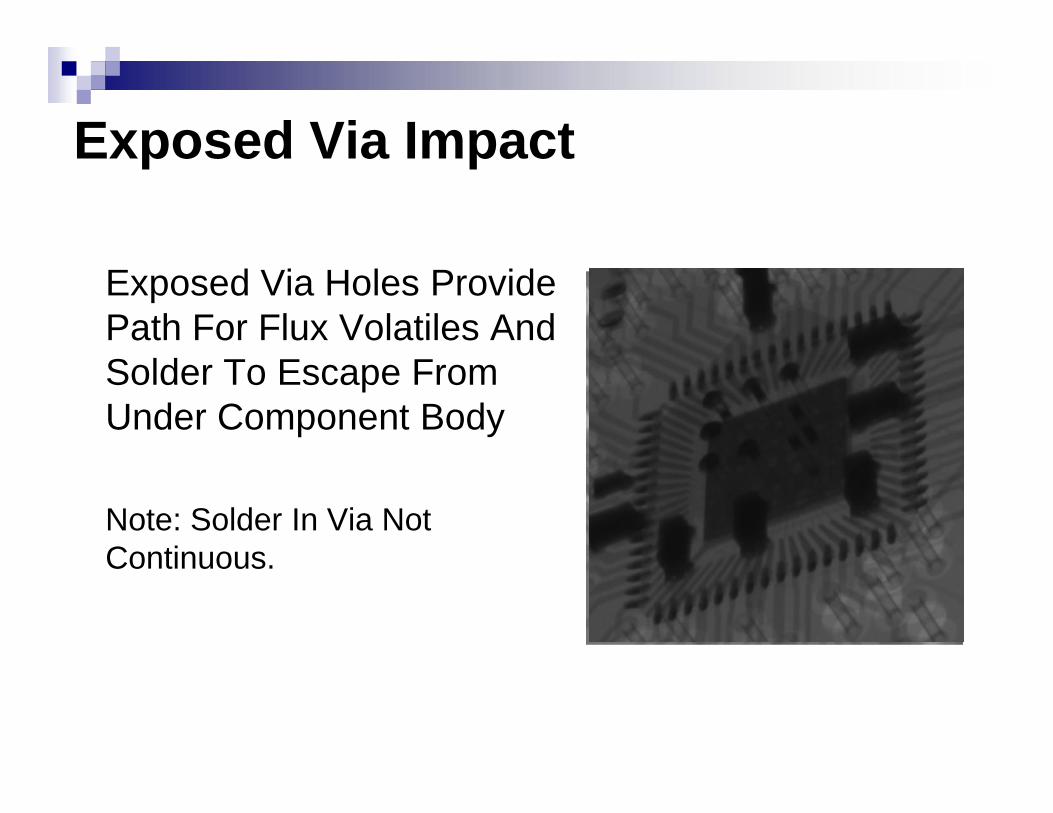
Exposed Via Impact
Exposed Via Holes ProvidePath For Flux Volatiles AndSolder To Escape FromUnder Component Body
Note: Solder In Via NotContinuous.
Exposed Via Holes ProvidePath For Flux Volatiles AndSolder To Escape FromUnder Component Body
Note: Solder In Via NotContinuous.

Thermal Pad Void Formation
Live_Xray_Reflow_Subtitles.mp4
Courtesy OfKummerl, S.(June, 2014).Texas InstrumentsAdvancedPackagingTrends. SMSEmergingTechnologyForum.
Live_Xray_Reflow_Subtitles.mp4
Courtesy OfKummerl, S.(June, 2014).Texas InstrumentsAdvancedPackagingTrends. SMSEmergingTechnologyForum.

Voids In Thermal Pad
Void Size andQuantity DecreaseWith IncreasedNumber Of ExposedVia Holes InThermal Pad
Void Size andQuantity DecreaseWith IncreasedNumber Of ExposedVia Holes InThermal Pad


Design Options
5 primary options recommended by IPC 7093 and component supplier guides
28

New Design Point: SMD Windows
29 Design Rule Parameters Controlled
29
Incorporates solder mask defined windows within the thermal pad area and I/O leads Utilize low cost open through-hole via structures Eliminate solder wicking down thermal vias Ensure proper via counts to manage heat/power Maximize thermal pad % coverage with solder Reduce stand-off variability; improving reliability Provide proper ground return paths, ensuring long term electrically stable system operation Enable safe, repeatable rework process windows
Kelly, Matt et al, “Via-In-Pad Design Considerations for Bottom Terminated Components on Printed Circuit Board Assemblies”, SMTAI 2013, Rosemont, IL.

Solder Preforms – Thermal Pad Offers Predictable Solder Volume Same Metallic Properties As Solder
Paste Flux Coating Compatible With Solder
Paste Size Engineered To Component Increased Standoff Height
Offers Predictable Solder Volume Same Metallic Properties As Solder
Paste Flux Coating Compatible With Solder
Paste Size Engineered To Component Increased Standoff Height
Homer, Seth et al, “Minimizing Voiding In QFN Packages Using Solder Preforms”, APEX Proceedings 2012, Las Vegas, NV.

Design For Cleaning
Removal Of Solder Mask Improves AbilityTo Clean Flux Residues From UnderComponent Body – Increase Stand-off

QFN/MLF Components
Flux Residue Is Heavy For AllSolder Masks
Gap Height Is Better For No Solder Mask Pads Strategies For Increasing Gap
Height Needed To Clean No Solder Mask Is Best Strategy
Time In Wash Is A CriticalParameter
Flux Residue Is Heavy For AllSolder Masks
Gap Height Is Better For No Solder Mask Pads Strategies For Increasing Gap
Height Needed To Clean No Solder Mask Is Best Strategy
Time In Wash Is A CriticalParameter

BGA Components Flux Residue Is Lower For
SMD & NSMD Pads
On No Solder Mask Pads Flux Flows Away From Solder Ball Penetrates Into Mask More Challenging To Clean
To Clean SMD Best NSMD 2nd Best No Solder Mask Worst
Flux Residue Is Lower For SMD & NSMD Pads
On No Solder Mask Pads Flux Flows Away From Solder Ball Penetrates Into Mask More Challenging To Clean
To Clean SMD Best NSMD 2nd Best No Solder Mask Worst

QFN Gap Height
MLF88 Singe RowMLF124 Double Row
110
100
90
80
STANDARDSQUARESLOTHEXAGON
NSMDNoSM
110
100
90
80
2560
Component
Ga
pH
eig
ht
(µm
)M
ea
n
Ground Plane Pattern
Solder Mask Definition Via Holes
Main Effects Plot for Gap Height (µm)Data Means
34
MLF88 Singe RowMLF124 Double Row
110
100
90
80
STANDARDSQUARESLOTHEXAGON
NSMDNoSM
110
100
90
80
2560
Component
Ga
pH
eig
ht
(µm
)M
ea
n
Ground Plane Pattern
Solder Mask Definition Via Holes
Main Effects Plot for Gap Height (µm)Data Means

Exposed Via Hole Impact Increase Number Of Via Holes In Thermal
Pad Results In:Fewer Voids In Thermal PadLess Flux Residue Under Component BodyDecreased Component Stand-off Height
Increase Number Of Via Holes In ThermalPad Results In:Fewer Voids In Thermal PadLess Flux Residue Under Component BodyDecreased Component Stand-off Height

Summary Lack Of Standard Definition For This Component Variability In Package Design Increases Complexity In
Assembly Process Requirements Manufacturing Tolerances For High Yield Tighter Than
Current Industry Material Standards Increased Number Of Via Holes In Thermal Pad
Decreases Voiding Increased Number Of Via Holes In Thermal Pad
Decreases Stand-off Height For Same Solder PasteCoverage Percentage
Cleaning Improves With Increase Stand-off Height AndRemoval Of Solder Mask On QFN’s And Solder MaskDefined Pads on BGA’s
Lack Of Standard Definition For This Component Variability In Package Design Increases Complexity In
Assembly Process Requirements Manufacturing Tolerances For High Yield Tighter Than
Current Industry Material Standards Increased Number Of Via Holes In Thermal Pad
Decreases Voiding Increased Number Of Via Holes In Thermal Pad
Decreases Stand-off Height For Same Solder PasteCoverage Percentage
Cleaning Improves With Increase Stand-off Height AndRemoval Of Solder Mask On QFN’s And Solder MaskDefined Pads on BGA’s

Thank You!
Questions


