Can testers and probe cards keep up with speed requirements for
image sensors?
FormFactor Inc. Larry LevyNobuhiro Kawamata
Advantest Corporation. Akira Hamajima
Abstract
2
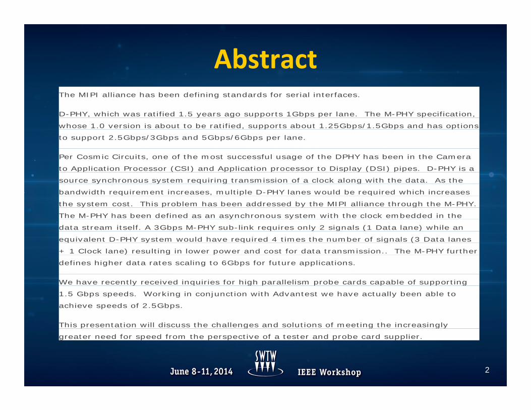
The MIPI alliance has been defining standards for serial interfaces.
D-PHY, which was ratified 1.5 years ago supports 1Gbps per lane. The M-PHY specification,
whose 1.0 version is about to be ratified, supports about 1.25Gbps/1.5Gbps and has options
to support 2.5Gbps/3Gbps and 5Gbps/6Gbps per lane.
Per Cosmic Circuits, one of the most successful usage of the DPHY has been in the Camera
to Application Processor (CSI) and Application processor to Display (DSI) pipes. D-PHY is a
source synchronous system requiring transmission of a clock along with the data. As the
bandwidth requirement increases, multiple D-PHY lanes would be required which increases
the system cost. This problem has been addressed by the MIPI alliance through the M-PHY.
The M-PHY has been defined as an asynchronous system with the clock embedded in the
data stream itself. A 3Gbps M-PHY sub-link requires only 2 signals (1 Data lane) while an
equivalent D-PHY system would have required 4 times the number of signals (3 Data lanes
+ 1 Clock lane) resulting in lower power and cost for data transmission.. The M-PHY further
defines higher data rates scaling to 6Gbps for future applications.
We have recently received inquiries for high parallelism probe cards capable of supporting
1.5 Gbps speeds. Working in conjunction with Advantest we have actually been able to
achieve speeds of 2.5Gbps.
This presentation will discuss the challenges and solutions of meeting the increasingly
greater need for speed from the perspective of a tester and probe card supplier.
Contents• High speed driver• Terms/ Definitions• Standards• Requirements• Tester interconnection and Loss• Probe card interconnection and Loss of 1.3Gbps/3Gbps designs– Probe Head– Probe card board
• Follow on works3

High Speed Drivers
Capture Stunning Videoin 1080p HD
Nokia Lumia Icon20 MP camera
LG G212 MP camera
The large 5.2” Full HD 1080p IPS display offersthe superior clarity of 423-pixel-per-inch resolution to deliver extraordinary
graphics and sharp text, all with the beauty of true-to-life colors.
16:9 high-definition
Samsung Galaxy 4S16 MP camera
Samsung has put everything it knows about HDTV on brilliant display with the 5.1-inch Full HD Super AMOLED® screen on the Galaxy S5. Movies come to life as they were meant to be seen
4

More Data Drives Need for Higher Speed
• Display resolution increasing for video and still– 1080P
• In July 2008, the ATSC standards were amended to include H.264/MPEG‐4 AVC compression and 1080p at 50, 59.94 and 60 frames per second (1080p50 and1080p60). Source: wikipedia
• More Megapixels in cameras• Need to take multiple pictures to get one good high resolution picture
5
Terms/ Definitions• Frame rate: Number of still images that make up one second's worth of video or animation– Frames per second "fps", is a measure of frame rate– The higher the frames per second value, the smoother the video (or animation) will appear
• 30fps or faster is typical for smooth video, while 15fps or lower will have noticeable flicker or choppiness.
• Bit rate: Number of bits processed/sec– 1 Gbit/s (one gigabit or one billion bits per second) = 1,000,000,000 bit/s rate
• D PHY – MIPI Alliance Standard for interface• M PHY‐MIPI Alliance Standard for interface
6
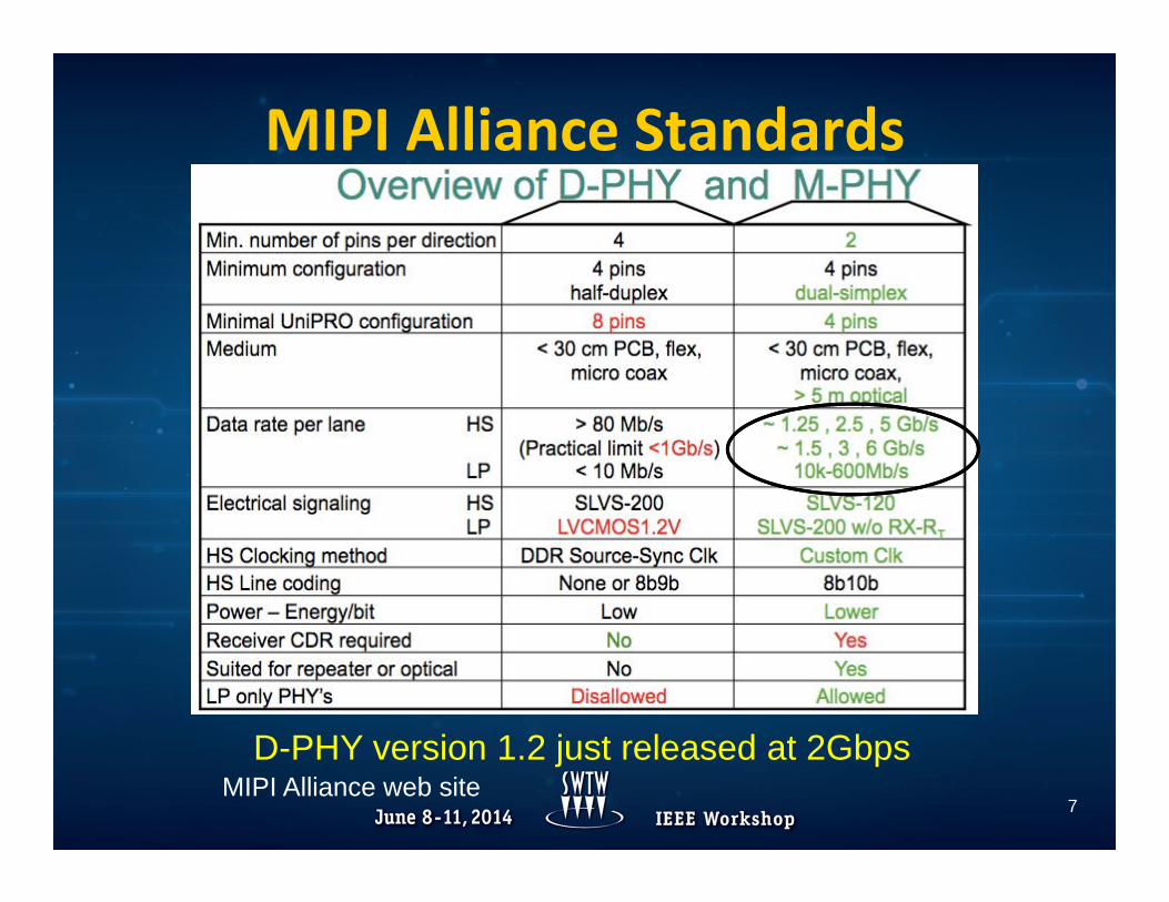
MIPI Alliance Standards
7MIPI Alliance web site
D-PHY version 1.2 just released at 2Gbps
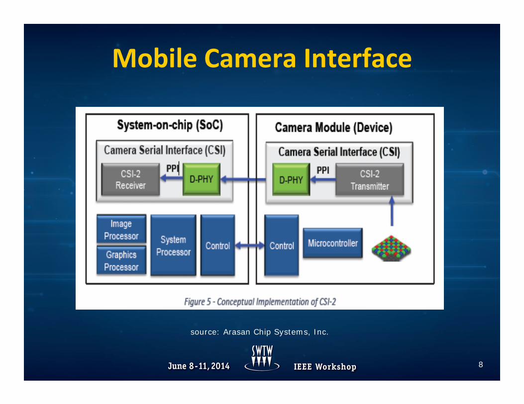
Mobile Camera Interface
8
source: Arasan Chip Systems, Inc.
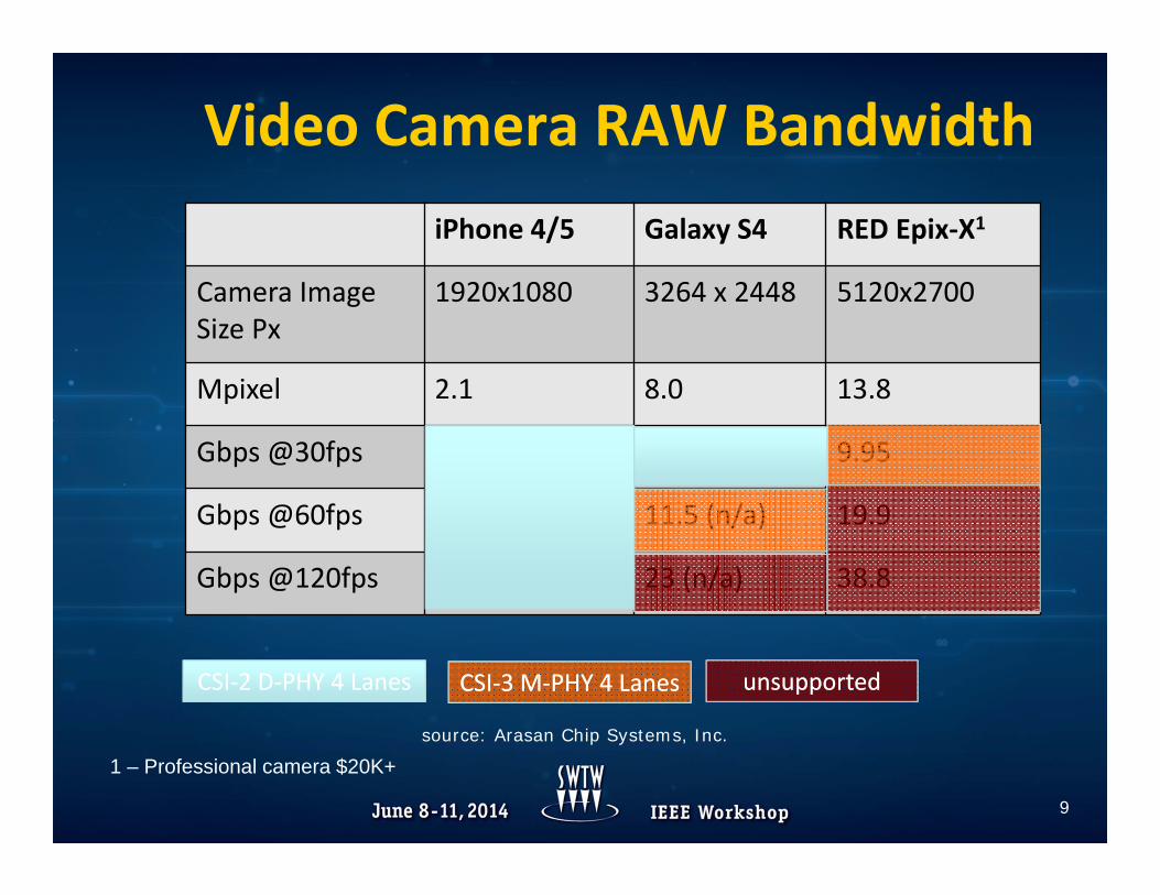
Video Camera RAW BandwidthiPhone 4/5 Galaxy S4 RED Epix‐X1
Camera ImageSize Px
1920x1080 3264 x 2448 5120x2700
Mpixel 2.1 8.0 13.8
Gbps @30fps 1.51 5.76 9.95
Gbps @60fps 3.0 (n/a) 11.5 (n/a) 19.9
Gbps @120fps 6.0 (n/a) 23 (n/a) 38.8
1 – Professional camera $20K+
CSI‐2 D‐PHY 4 LanesCSI‐2 D‐PHY 4 Lanes CSI‐3 M‐PHY 4 LanesCSI‐3 M‐PHY 4 Lanes unsupportedunsupported
9
source: Arasan Chip Systems, Inc.
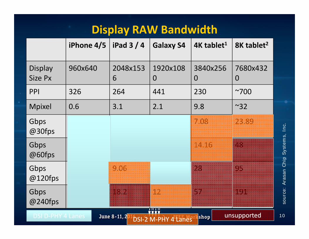
Display RAW BandwidthiPhone 4/5 iPad 3 / 4 Galaxy S4 4K tablet1 8K tablet2
Display Size Px
960x640 2048x1536
1920x1080
3840x2560
7680x4320
PPI 326 264 441 230 ~700
Mpixel 0.6 3.1 2.1 9.8 ~32
Gbps @30fps
0.44 2.27 1.49 7.08 23.89
Gbps @60fps
0.89 4.53 2.99 14.16 48
Gbps @120fps
1.77 9.06 5.97 28 95
Gbps @240fps
3.54 18.2 12 57 191
DSI D‐PHY 4 LanesDSI D‐PHY 4 Lanes DSI‐2 M‐PHY 4 LanesDSI‐2 M‐PHY 4 Lanes unsupportedunsupported 10
sour
ce:
Ara
san
Chi
p Sy
stem
s, I
nc.

Need for Speed
Are you convinced that we need higher speed?
11
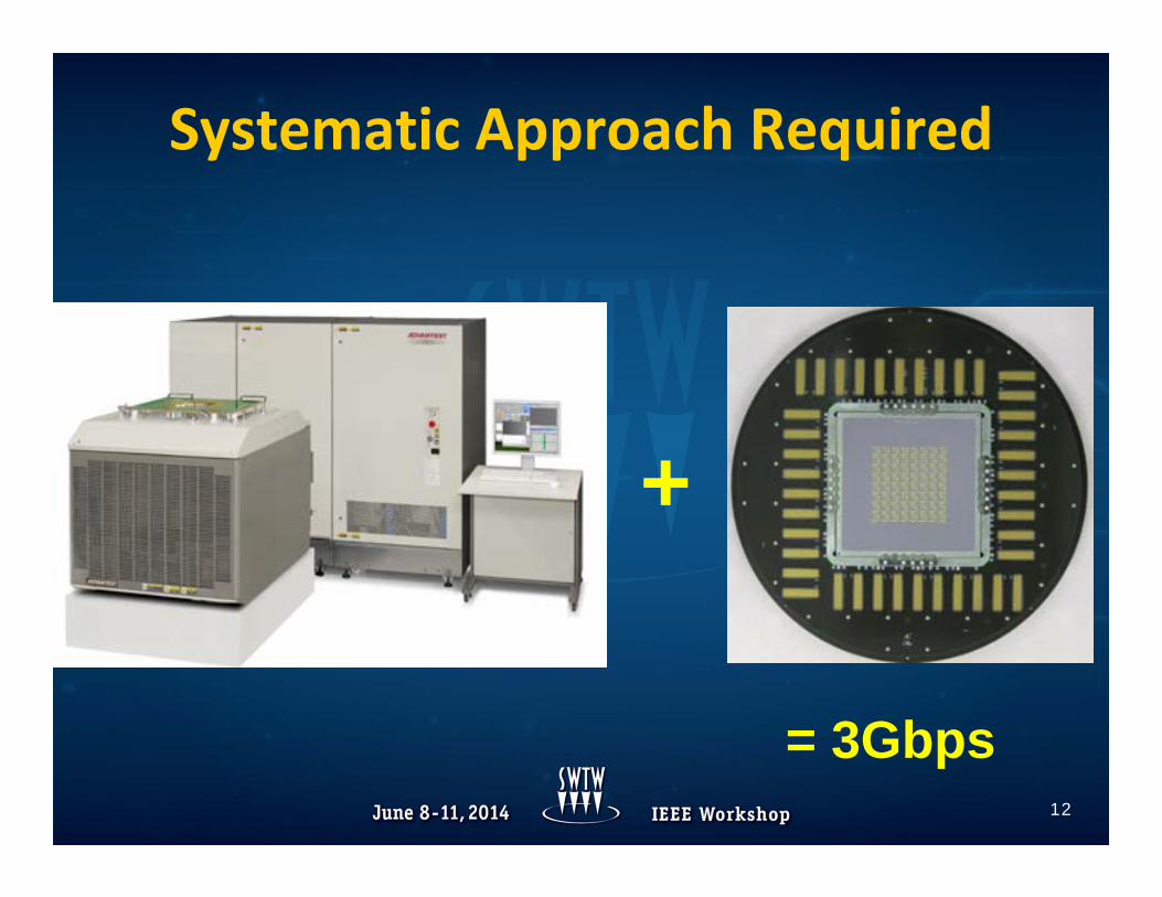
Systematic Approach Required
12
+
= 3Gbps

Interconnection Loss Specification in D‐PHY
• Data rate <=1.5Gbps, loss requirement is less than ‐2db• Data rate >1.5Gbps, loss requirement is less than ‐3.75db
• Goals: Tester side ‐1.75db, Probe Card ‐2db, Total ‐3.75db loss with 50 Ohm impedance
13
* fh = Data Rate/2
Probe Card
Probe Card Board
Probe Head
Tester Interconnection
HIFIX Cable
Performance Board
Frog Unit
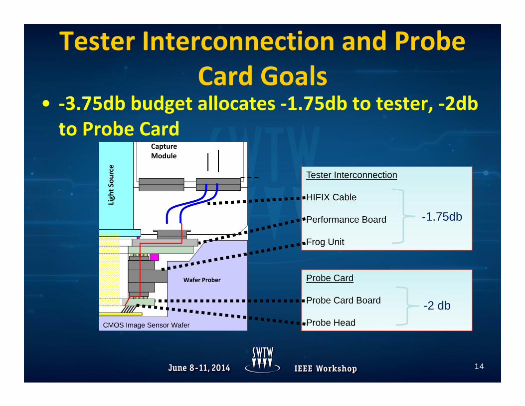
Tester Interconnection and Probe Card Goals
• ‐3.75db budget allocates ‐1.75db to tester, ‐2db to Probe Card
14
Light S
ource
Wafer Prober
CaptureModule
CMOS Image Sensor Wafer
-1.75db
-2 db
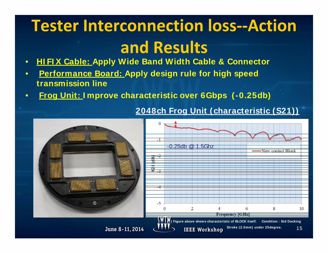
Tester Interconnection loss‐‐Action and Results
• HIFIX Cable: Apply Wide Band Width Cable & Connector• Performance Board: Apply design rule for high speed
transmission line• Frog Unit: Improve characteristic over 6Gbps (-0.25db)
15(*) Figure above shows characteristic of BLOCK itself. Condition : Std Docking
Stroke (2.0mm) under 25degree.
2048ch Frog Unit (characteristic (S21))
-0.25db @ 1.5Ghz

Probe Card Loss‐‐‐ Phase 1 Action and Results
16
• Design Method PH: LGA between the DUT, MIPI differential pair trace length shortened
• Design Rule All: HFTAP high speed transmission line design rule
800Mbps Design 1.2Gbps Design
800Mbps Design 1.2Gbps Design
Parallelism 20 64
Probe Head ‐1.12 to ‐0.72 (dB) ‐0.67 to ‐0.49 (dB)
PCB ‐3.4dB ‐2.3dB
Total Probe Card Loss ‐4db ‐3db

Probe card loss ‐‐‐Phase 2 Action and measurement plan
17
Measurement point
Design Method PH: More LGA between the DUT, MIPI differential pair trace
PCB: Trace improvement for differential pair, and back drilling
Design Rule All: New HFTAP high speed transmission line design rule
Measurements:PH only, PCB Only, Total Probe Card
Frog Unit
PH
PCB
Card

Measurement Method and Points• Measurement: Open ended rise time measurement by TDR 20‐80%, 10 measurement points
Probe Head Only Probe card (PH+PCB)
18
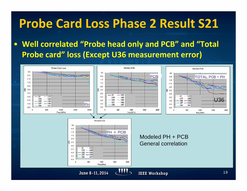
Probe Card Loss Phase 2 Result S21• Well correlated “Probe head only and PCB” and “Total Probe card” loss (Except U36 measurement error)
PH
TOTAL PCB + PHPCB
PH + PCB
19
Modeled PH + PCBGeneral correlation
U36
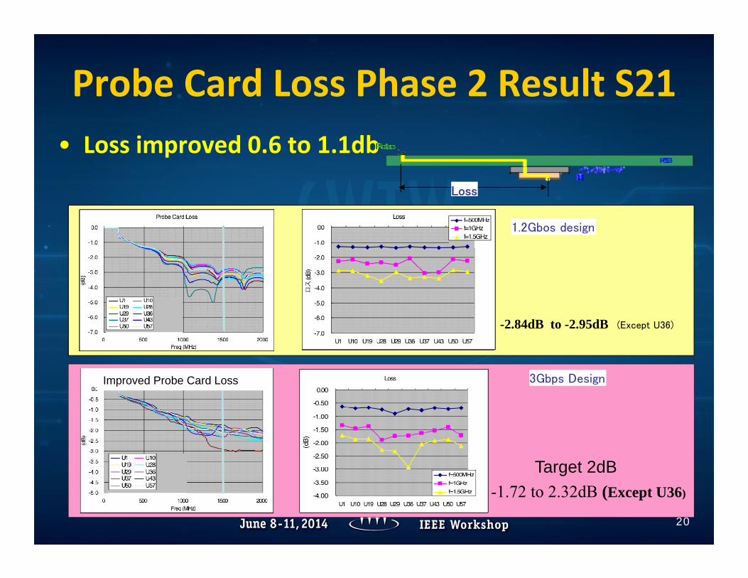
Probe Card Loss Phase 2 Result S21• Loss improved 0.6 to 1.1db
20
1.2Gbos design
Loss
-2.84dB to -2.95dB (Except U36)
3Gbps Design
-1.72 to 2.32dB (Except U36)
Target 2dB
Improved Probe Card Loss
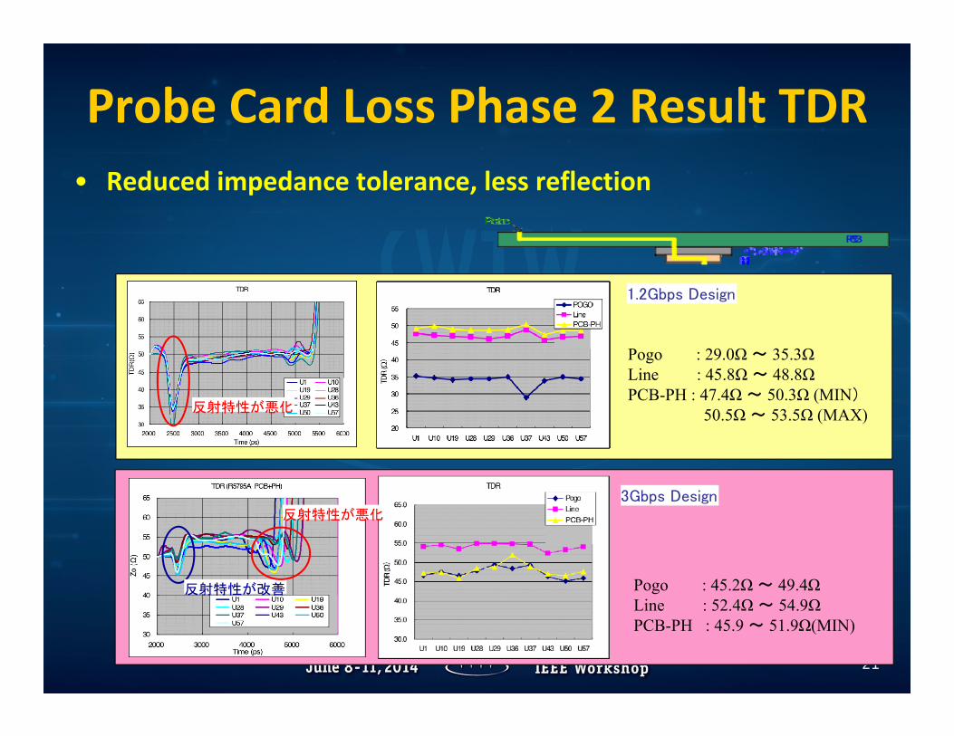
Probe Card Loss Phase 2 Result TDR• Reduced impedance tolerance, less reflection
21
1.2Gbps Design
Pogo : 29.0Ω ~ 35.3ΩLine : 45.8Ω ~ 48.8ΩPCB-PH : 47.4Ω ~ 50.3Ω (MIN)
50.5Ω ~ 53.5Ω (MAX)
3Gbps Design
Pogo : 45.2Ω ~ 49.4ΩLine : 52.4Ω ~ 54.9Ω PCB-PH : 45.9 ~ 51.9Ω(MIN)
反射特性が悪化
反射特性が改善
反射特性が悪化

Probe Card Loss Phase 2 Results Summary
22
Loss @ F=1.5Ghz Typical Design Rules(ie <1.2Gbps)
3Gbps Design Rules
Parallelism 64 64
Total Probe Card S21 Loss ‐3db* 1.72 to 2.32dB
3Gbps S21 Loss Goal ‐2db
Judgment Fail* Acceptable with minor adjustments
Total Probe Card Impedance @ Tr100ps Pogo: 45.2 to 49.4ΩPCB: 45.9 to 51.9Ω
3Gbps S21 Loss Goal 47‐53Ω
Judgment Fail* Acceptable
*Prevailing design rules found not to be sufficient to achieve higher speeds

Follow On Works
• Light source keep‐out area on PCB reduction by developing LED light source
• Advanced Probe Card Material and design rule implementation
23


