Download - Chap9-Bipolar Logic Circuits
Jaeger/Blalock10/21/03
Microelectronic Circuit DesignMcGraw-Hill
Chap 9 - 1
Chapter 9Bipolar Logic Circuits
Microelectronic Circuit DesignRichard C. JaegerTravis N. Blalock
Jaeger/Blalock10/21/03
Microelectronic Circuit DesignMcGraw-Hill
Chap 9 - 2
Chapter Goals
• Bipolar switch circuits
• Emitter-coupled logic (ECL)
• Behavior of the bipolar transistor as a saturated switch
• Transistor-transistor logic (TTL)
• Schottky clamping techniques for preventing saturation
• Operation of the transistor in the inverse-active region
• Voltage reference design
• BiCMOS logic circuits
Jaeger/Blalock10/21/03
Microelectronic Circuit DesignMcGraw-Hill
Chap 9 - 3
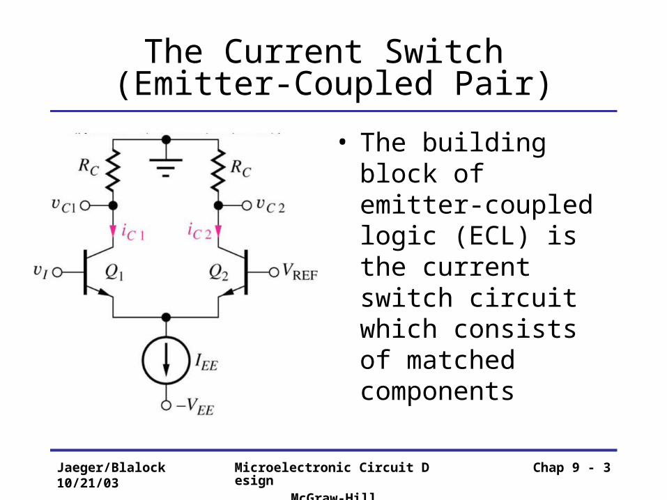
The Current Switch (Emitter-Coupled Pair)
• The building block of emitter-coupled logic (ECL) is the current switch circuit which consists of matched components
Jaeger/Blalock10/21/03
Microelectronic Circuit DesignMcGraw-Hill
Chap 9 - 4
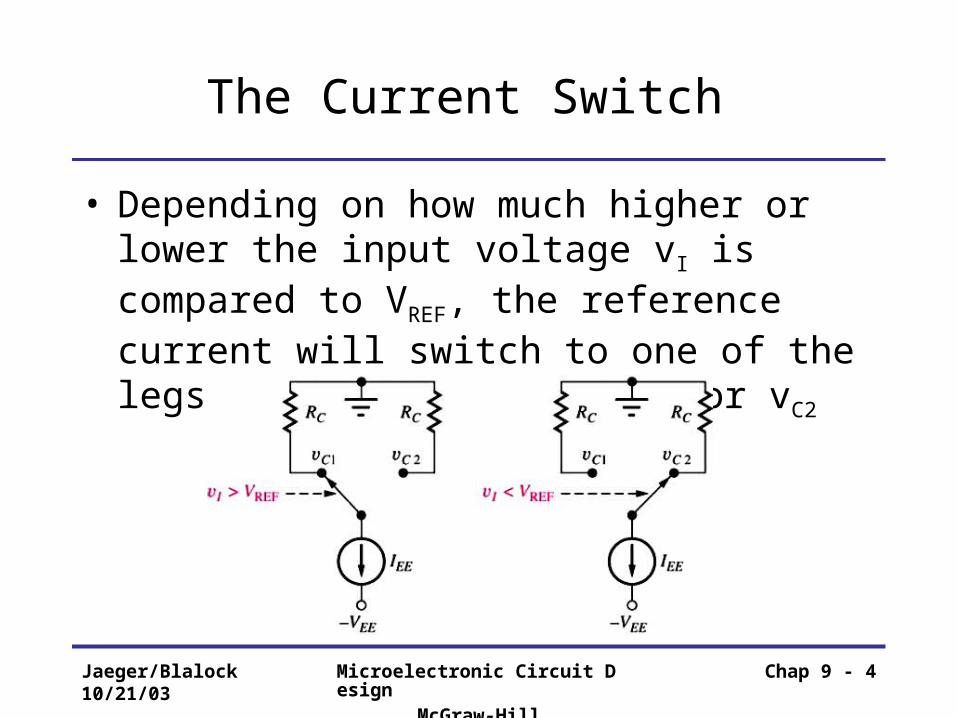
The Current Switch
• Depending on how much higher or lower the input voltage vI is compared to VREF, the reference current will switch to one of the legs creating a voltage vC1or vC2
Jaeger/Blalock10/21/03
Microelectronic Circuit DesignMcGraw-Hill
Chap 9 - 5
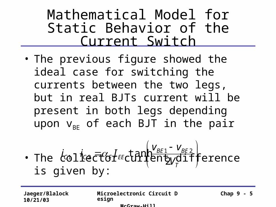
Mathematical Model for Static Behavior of the Current Switch
• The previous figure showed the ideal case for switching the currents between the two legs, but in real BJTs current will be present in both legs depending upon vBE of each BJT in the pair
• The collector current difference is given by:
T
BEBEEEFCC V
vvIii
2tanh 21
21
Jaeger/Blalock10/21/03
Microelectronic Circuit DesignMcGraw-Hill
Chap 9 - 6
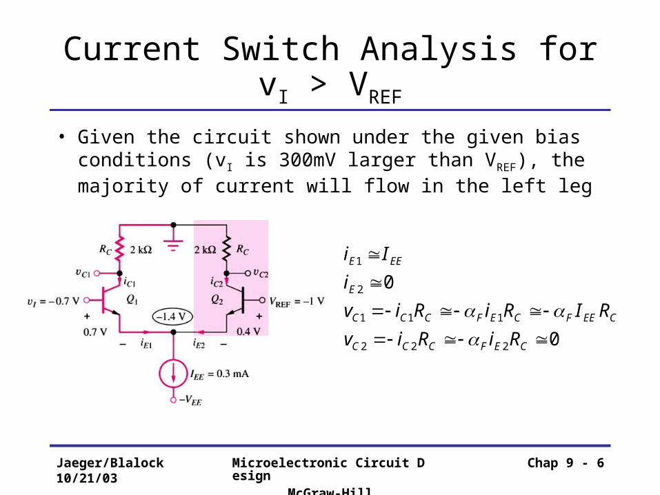
Current Switch Analysis for vI > VREF
• Given the circuit shown under the given bias conditions (vI is 300mV larger than VREF), the majority of current will flow in the left leg
0
0
222
111
2
1
CEFCCC
CEEFCEFCCC
E
EEE
RiRiv
RIRiRiv
i
Ii
Jaeger/Blalock10/21/03
Microelectronic Circuit DesignMcGraw-Hill
Chap 9 - 7
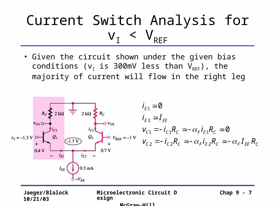
Current Switch Analysis for vI < VREF
• Given the circuit shown under the given bias conditions (vI is 300mV less than VREF), the majority of current will flow in the right leg
CEEFCEFCCC
CEFCCC
EEE
E
RIRiRiv
RiRiv
Ii
i
222
111
2
1
0
0
Jaeger/Blalock10/21/03
Microelectronic Circuit DesignMcGraw-Hill
Chap 9 - 8
The Emitter-Coupled Logic (ECL) Gate
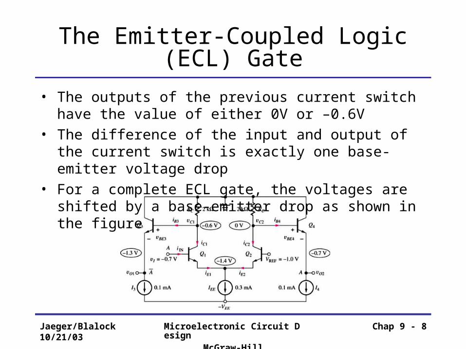
• The outputs of the previous current switch have the value of either 0V or –0.6V
• The difference of the input and output of the current switch is exactly one base-emitter voltage drop
• For a complete ECL gate, the voltages are shifted by a base-emitter drop as shown in the figure
Jaeger/Blalock10/21/03
Microelectronic Circuit DesignMcGraw-Hill
Chap 9 - 9
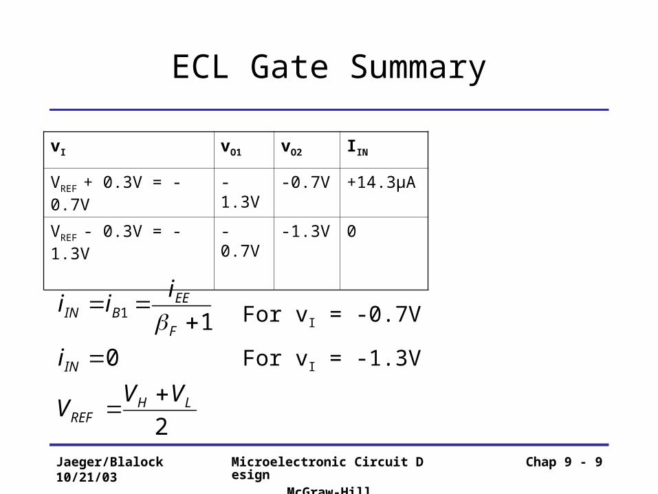
ECL Gate Summary
vI vO1 vO2 IIN
VREF + 0.3V = -0.7V -1.3V -0.7V +14.3µA
VREF - 0.3V = -1.3V -0.7V -1.3V 0
2
0
11
LHREF
IN
F
EEBIN
VVV
i
iii
For vI = -0.7V
For vI = -1.3V
Jaeger/Blalock10/21/03
Microelectronic Circuit DesignMcGraw-Hill
Chap 9 - 10
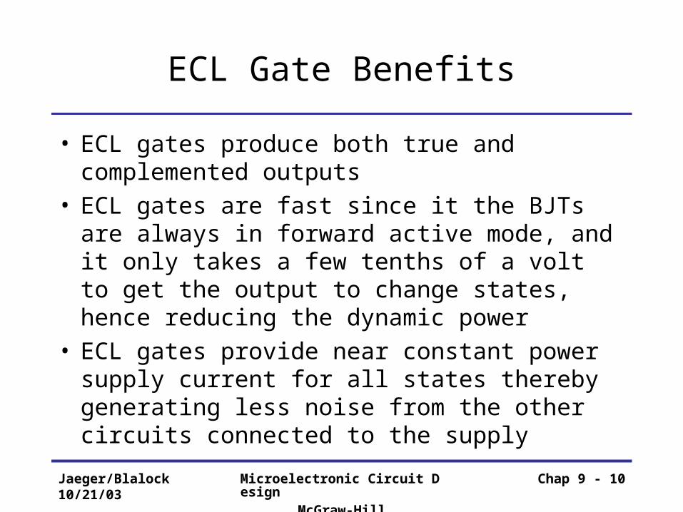
ECL Gate Benefits
• ECL gates produce both true and complemented outputs
• ECL gates are fast since it the BJTs are always in forward active mode, and it only takes a few tenths of a volt to get the output to change states, hence reducing the dynamic power
• ECL gates provide near constant power supply current for all states thereby generating less noise from the other circuits connected to the supply
Jaeger/Blalock10/21/03
Microelectronic Circuit DesignMcGraw-Hill
Chap 9 - 11
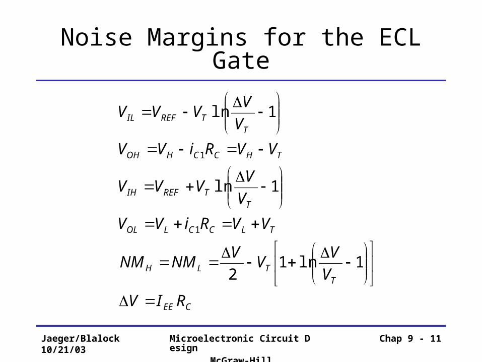
Noise Margins for the ECL Gate
CEE
TTLH
TLCCLOL
TTREFIH
THCCHOH
TTREFIL
RIV
V
VV
VNMNM
VVRiVV
V
VVVV
VVRiVV
V
VVVV
1ln12
1ln
1ln
1
1
Jaeger/Blalock10/21/03
Microelectronic Circuit DesignMcGraw-Hill
Chap 9 - 12
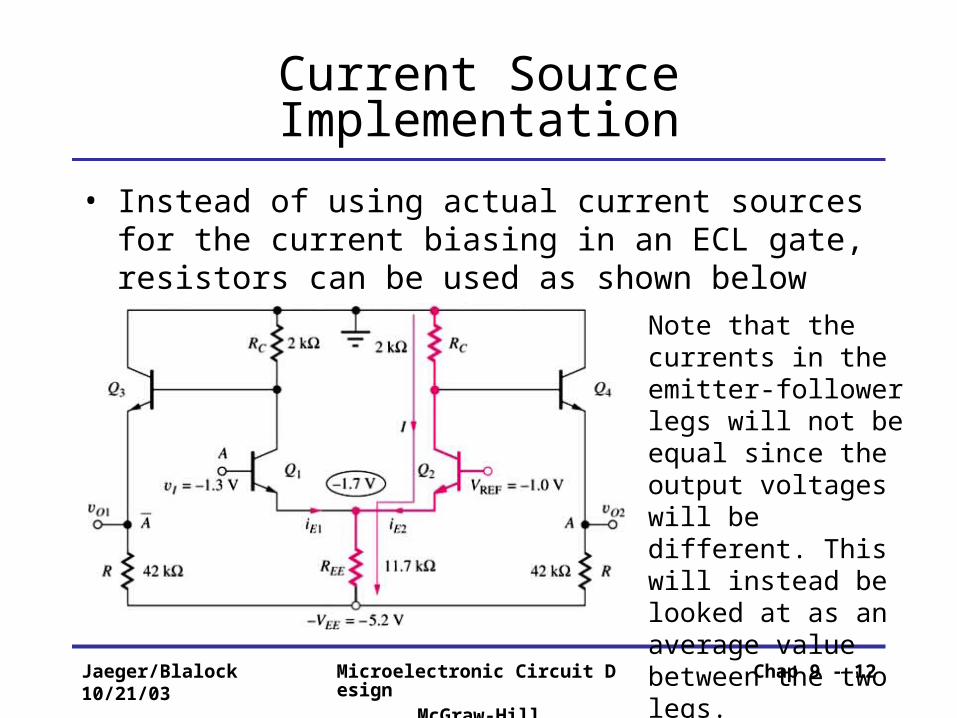
Current Source Implementation
• Instead of using actual current sources for the current biasing in an ECL gate, resistors can be used as shown below
Note that the currents in the emitter-follower legs will not be equal since the output voltages will be different. This will instead be looked at as an average value between the two legs.
Jaeger/Blalock10/21/03
Microelectronic Circuit DesignMcGraw-Hill
Chap 9 - 13
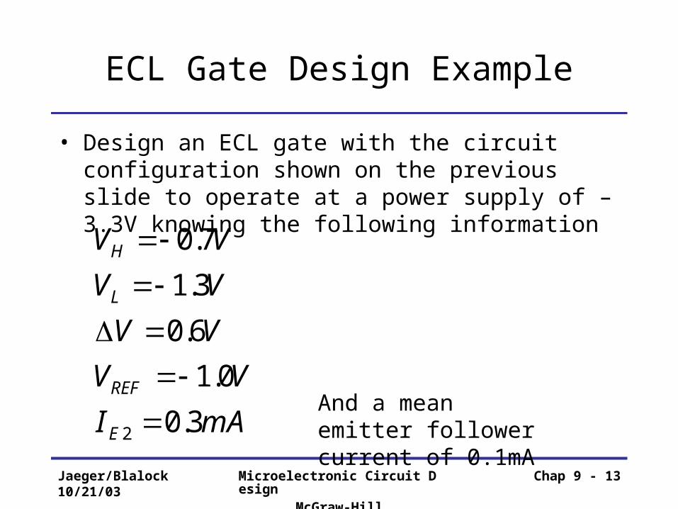
ECL Gate Design Example
• Design an ECL gate with the circuit configuration shown on the previous slide to operate at a power supply of –3.3V knowing the following information
mAI
VV
VV
VV
VV
E
REF
L
H
3.0
0.1
6.0
3.1
7.0
2
And a mean emitter follower current of 0.1mA
Jaeger/Blalock10/21/03
Microelectronic Circuit DesignMcGraw-Hill
Chap 9 - 14
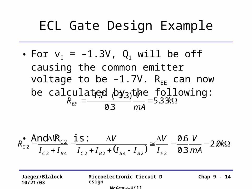
ECL Gate Design Example
• For vI = –1.3V, Q1 will be off causing the common emitter voltage to be –1.7V. REE can now be calculated by the following:
• And RC2 is:
kmA
VREE 33.5
3.0
)3.3(7.1
kmA
V
I
V
IIII
V
II
VR
EBBBCBCC 0.2
3.0
6.0
22422422
Jaeger/Blalock10/21/03
Microelectronic Circuit DesignMcGraw-Hill
Chap 9 - 15
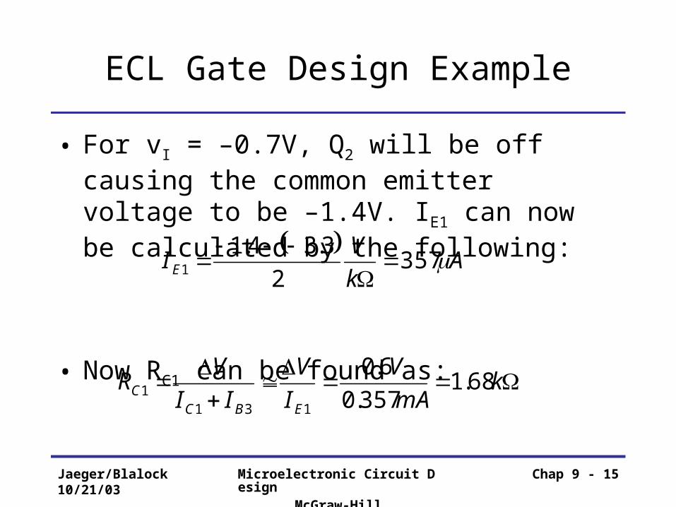
ECL Gate Design Example
• For vI = –0.7V, Q2 will be off causing the common emitter voltage to be –1.4V. IE1 can now be calculated by the following:
• Now RC1 can be found as:
A
k
VIE 357
2
3.34.11
k
mA
V
I
V
II
VR
EBCC 68.1
357.0
6.0
1311
Jaeger/Blalock10/21/03
Microelectronic Circuit DesignMcGraw-Hill
Chap 9 - 16
ECL Gate Design Example
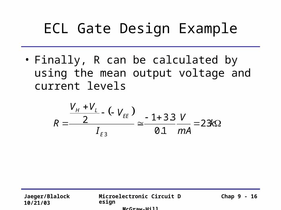
• Finally, R can be calculated by using the mean output voltage and current levels
kmA
V
I
VVV
RE
EELH
231.0
3.312
3
Jaeger/Blalock10/21/03
Microelectronic Circuit DesignMcGraw-Hill
Chap 9 - 17
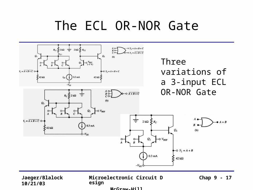
The ECL OR-NOR Gate
Three variations of a 3-input ECL OR-NOR Gate
Jaeger/Blalock10/21/03
Microelectronic Circuit DesignMcGraw-Hill
Chap 9 - 18
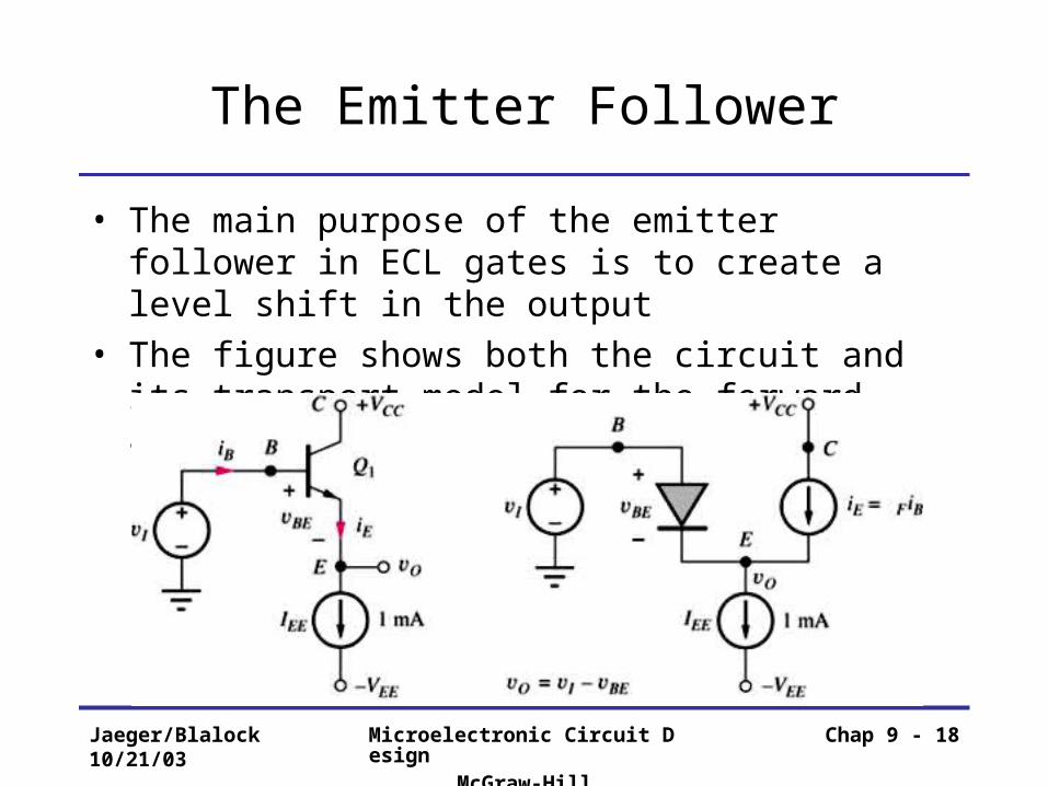
The Emitter Follower
• The main purpose of the emitter follower in ECL gates is to create a level shift in the output
• The figure shows both the circuit and its transport model for the forward- active region
Jaeger/Blalock10/21/03
Microelectronic Circuit DesignMcGraw-Hill
Chap 9 - 19
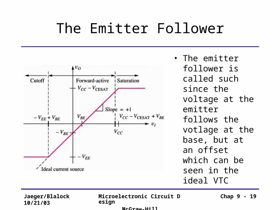
The Emitter Follower
• The emitter follower is called such since the voltage at the emitter follows the votlage at the base, but at an offset which can be seen in the ideal VTC
Jaeger/Blalock10/21/03
Microelectronic Circuit DesignMcGraw-Hill
Chap 9 - 20
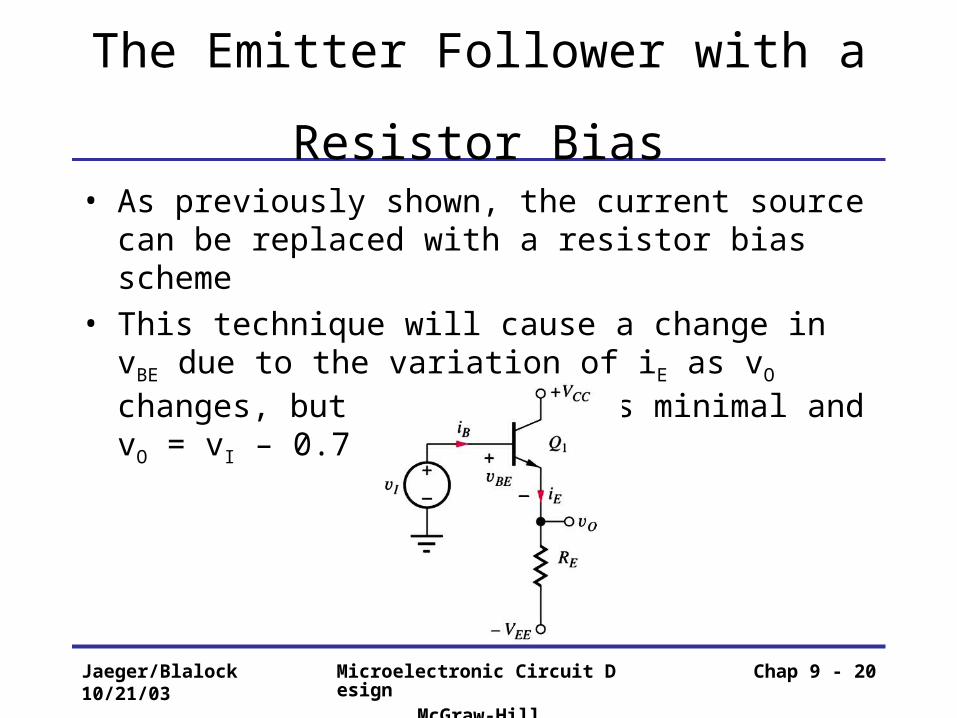
The Emitter Follower with a Resistor Bias
• As previously shown, the current source can be replaced with a resistor bias scheme
• This technique will cause a change in vBE due to the variation of iE as vO changes, but this change is minimal and vO = vI – 0.7
Jaeger/Blalock10/21/03
Microelectronic Circuit DesignMcGraw-Hill
Chap 9 - 21
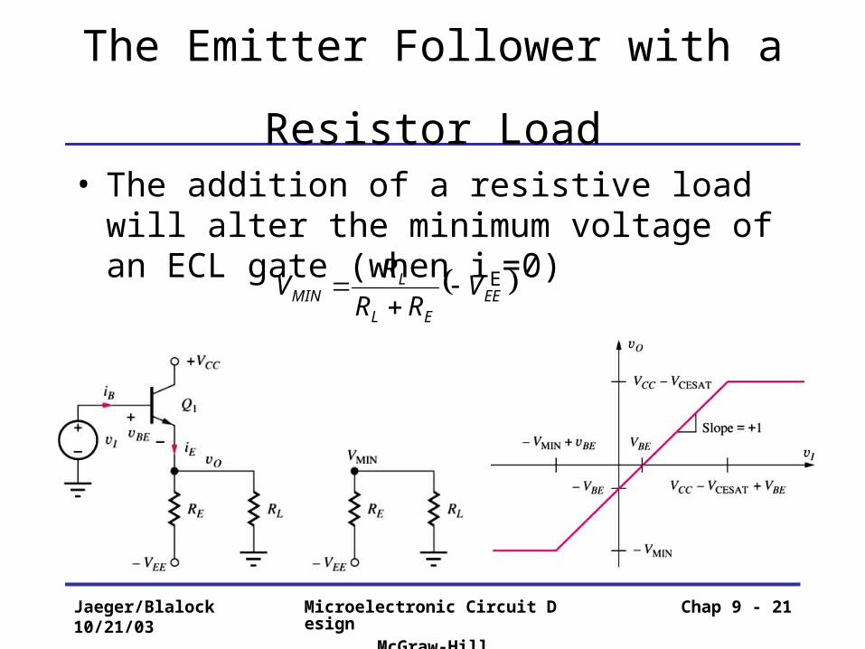
The Emitter Follower with a Resistor Load
• The addition of a resistive load will alter the minimum voltage of an ECL gate (when iE=0)
EEEL
LMIN V
RR
RV
Jaeger/Blalock10/21/03
Microelectronic Circuit DesignMcGraw-Hill
Chap 9 - 22
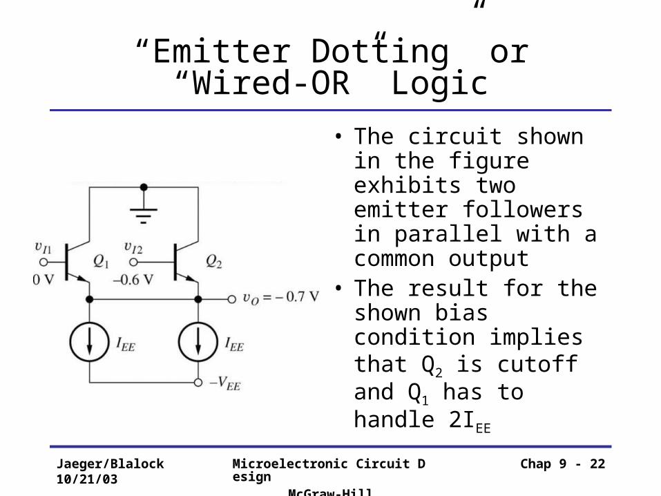
“Emitter Dotting” or “Wired-OR” Logic
• The circuit shown in the figure exhibits two emitter followers in parallel with a common output
• The result for the shown bias condition implies that Q2 is cutoff and Q1 has to handle 2IEE
Jaeger/Blalock10/21/03
Microelectronic Circuit DesignMcGraw-Hill
Chap 9 - 23
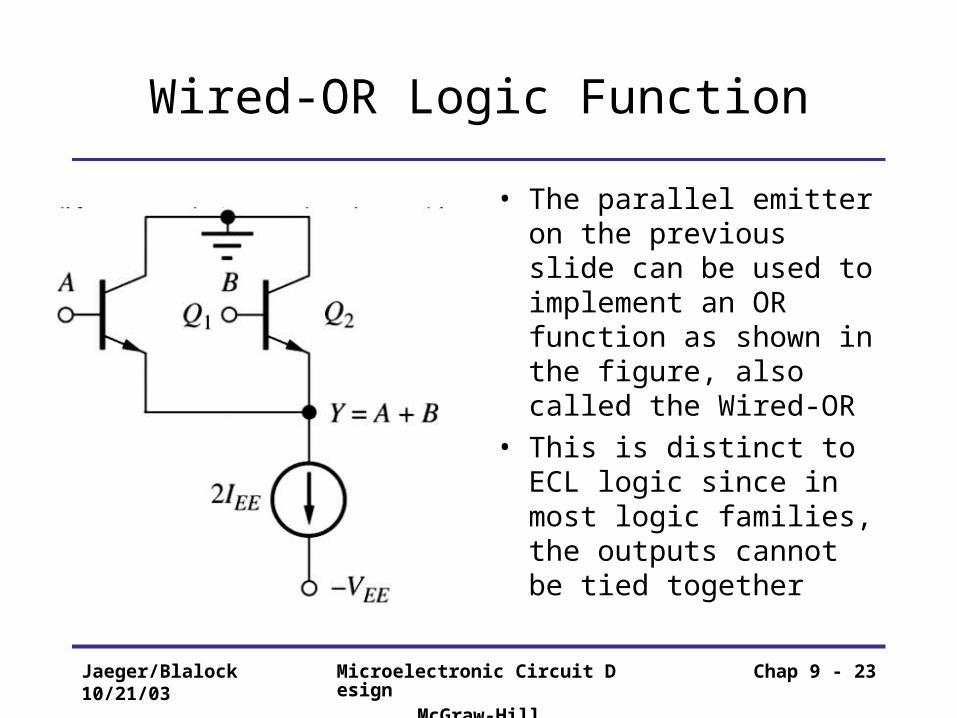
Wired-OR Logic Function
• The parallel emitter on the previous slide can be used to implement an OR function as shown in the figure, also called the Wired-OR
• This is distinct to ECL logic since in most logic families, the outputs cannot be tied together
Jaeger/Blalock10/21/03
Microelectronic Circuit DesignMcGraw-Hill
Chap 9 - 24
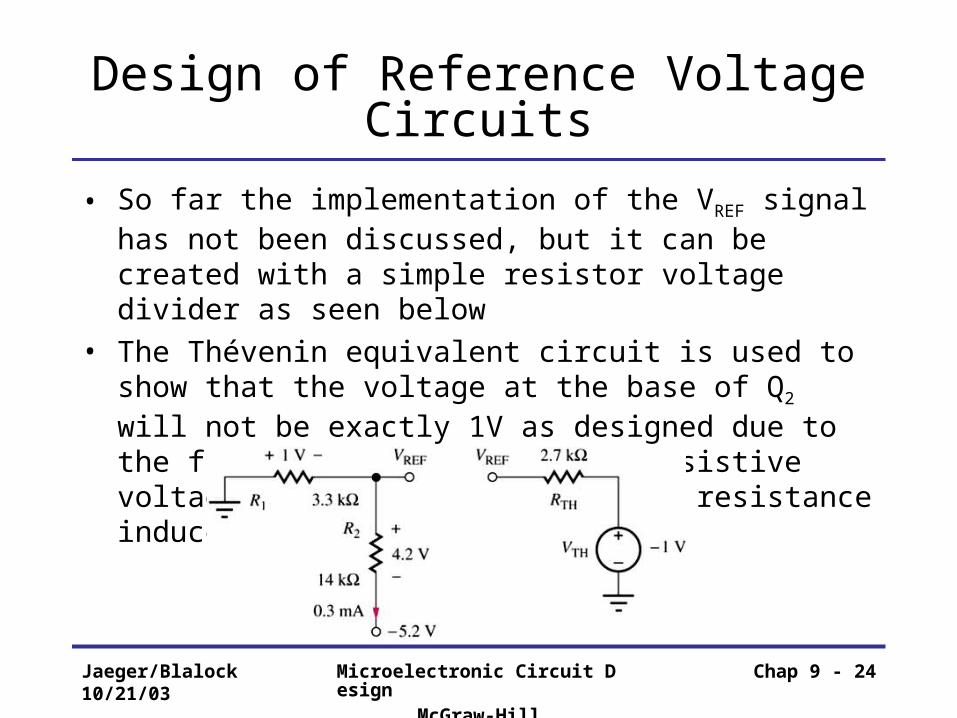
Design of Reference Voltage Circuits
• So far the implementation of the VREF signal has not been discussed, but it can be created with a simple resistor voltage divider as seen below
• The Thévenin equivalent circuit is used to show that the voltage at the base of Q2 will not be exactly 1V as designed due to the fact that there will be a resistive voltage drop across the Thévenin resistance induced by iB2
Jaeger/Blalock10/21/03
Microelectronic Circuit DesignMcGraw-Hill
Chap 9 - 25
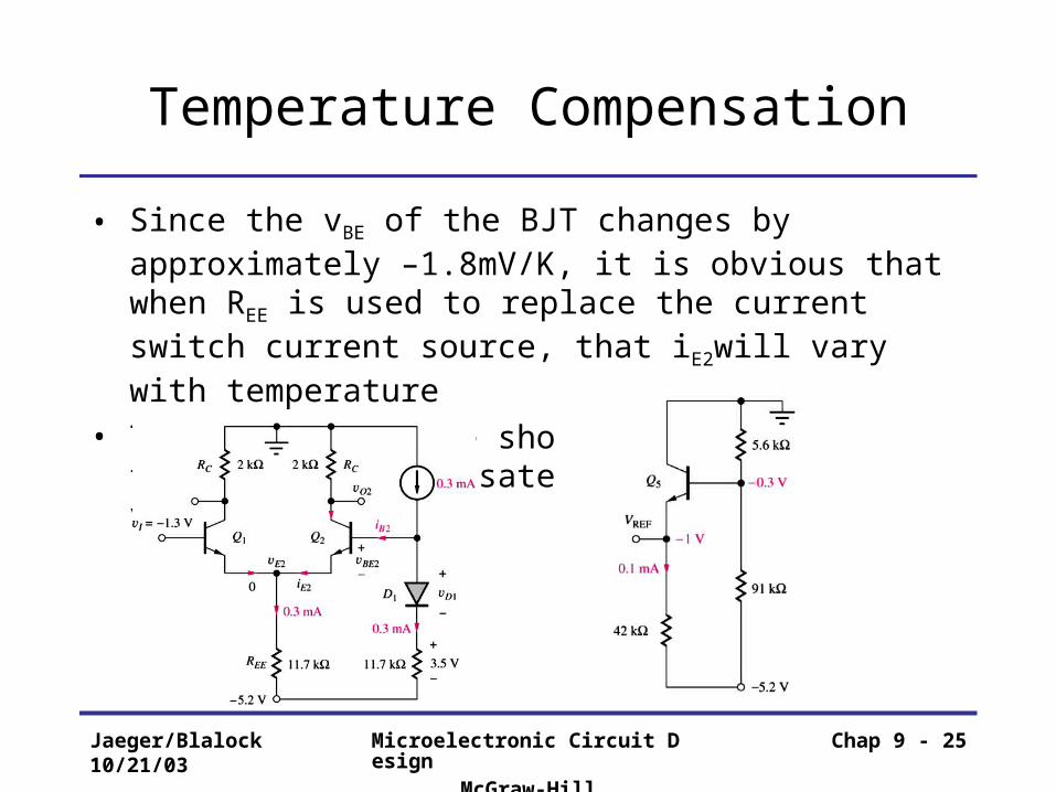
Temperature Compensation
• Since the vBE of the BJT changes by approximately –1.8mV/K, it is obvious that when REE is used to replace the current switch current source, that iE2will vary with temperature
• Two techniques are shown below that temperature compensate (track) the variation
Jaeger/Blalock10/21/03
Microelectronic Circuit DesignMcGraw-Hill
Chap 9 - 26
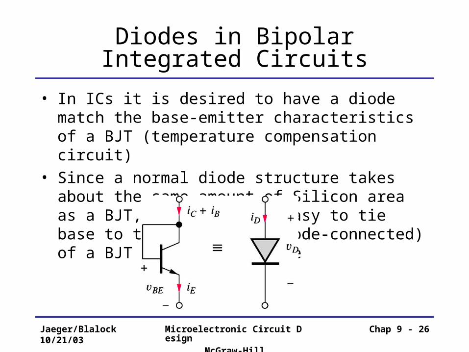
Diodes in Bipolar Integrated Circuits
• In ICs it is desired to have a diode match the base-emitter characteristics of a BJT (temperature compensation circuit)
• Since a normal diode structure takes about the same amount of Silicon area as a BJT, it is just as easy to tie base to the collector (diode-connected) of a BJT to create a diode
Jaeger/Blalock10/21/03
Microelectronic Circuit DesignMcGraw-Hill
Chap 9 - 27
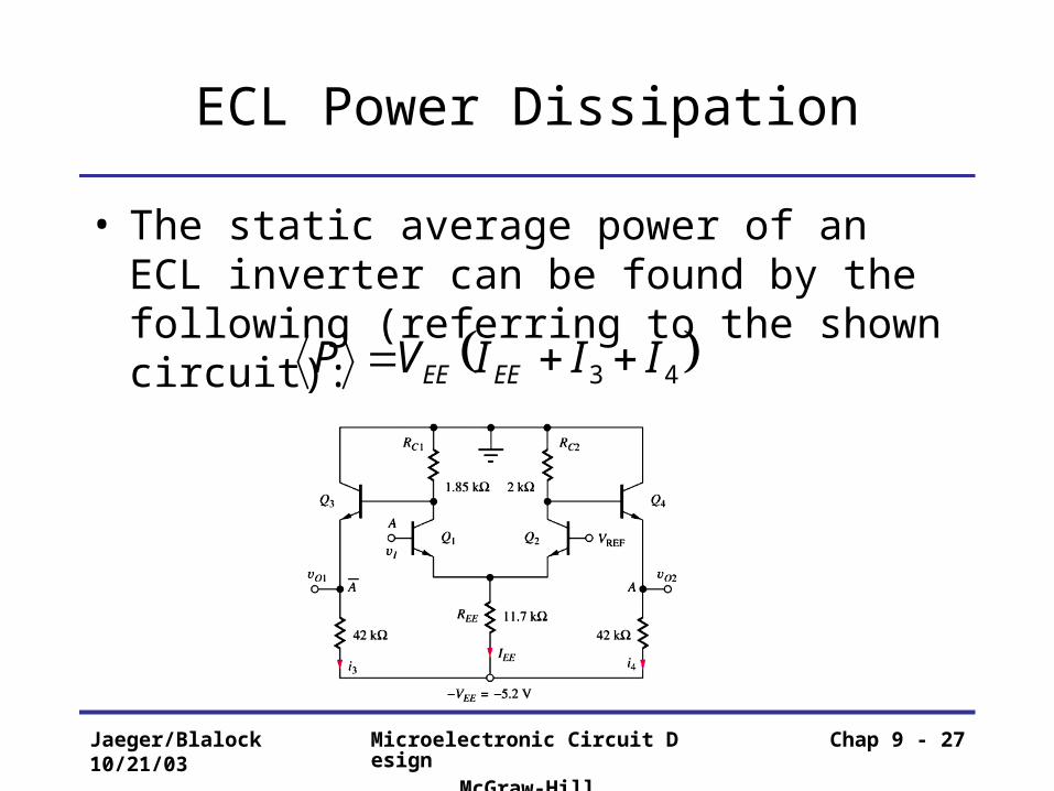
ECL Power Dissipation
• The static average power of an ECL inverter can be found by the following (referring to the shown circuit): 43 IIIVP EEEE
Jaeger/Blalock10/21/03
Microelectronic Circuit DesignMcGraw-Hill
Chap 9 - 28
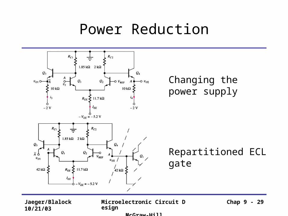
Power Reduction
• Approximately 40% of the power is dissipated by the emitter-follower stages
• One technique to reduce this current is to make the bias the emitter-follower resistors at a less negative value thereby reducing the current, however this requires an additional power supply
• Another technique is to share the current in the manner shown on the next slide (similar to the wired-OR), however any output that is not driving another logic gate needs to be terminated with a resistor to the negative power rail
Jaeger/Blalock10/21/03
Microelectronic Circuit DesignMcGraw-Hill
Chap 9 - 29
Power Reduction
Changing the power supply
Repartitioned ECL gate
Jaeger/Blalock10/21/03
Microelectronic Circuit DesignMcGraw-Hill
Chap 9 - 30
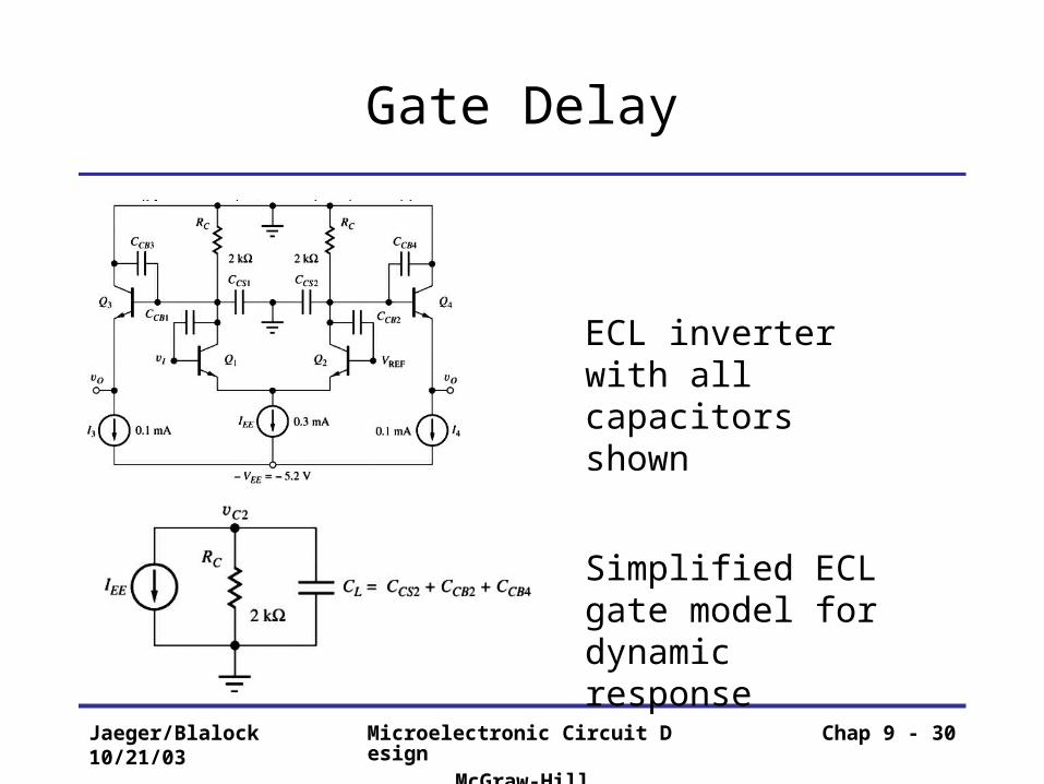
Gate Delay
ECL inverter with all capacitors shown
Simplified ECL gate model for dynamic response
Jaeger/Blalock10/21/03
Microelectronic Circuit DesignMcGraw-Hill
Chap 9 - 31
Gate Delay
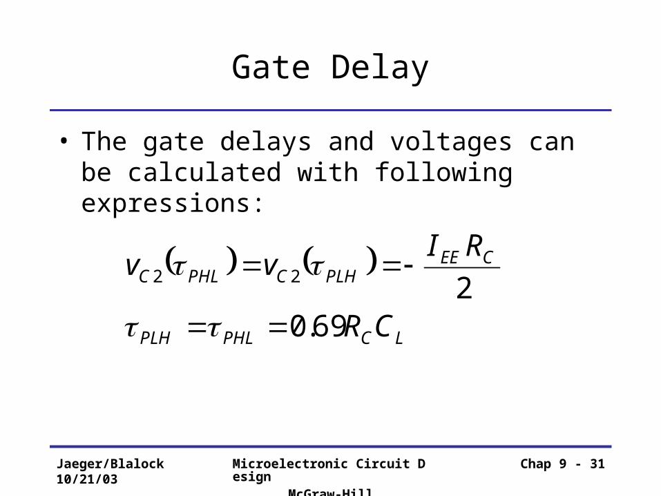
• The gate delays and voltages can be calculated with following expressions:
LCPHLPLH
CEEPLHCPHLC
CR
RIvv
69.0222
Jaeger/Blalock10/21/03
Microelectronic Circuit DesignMcGraw-Hill
Chap 9 - 32
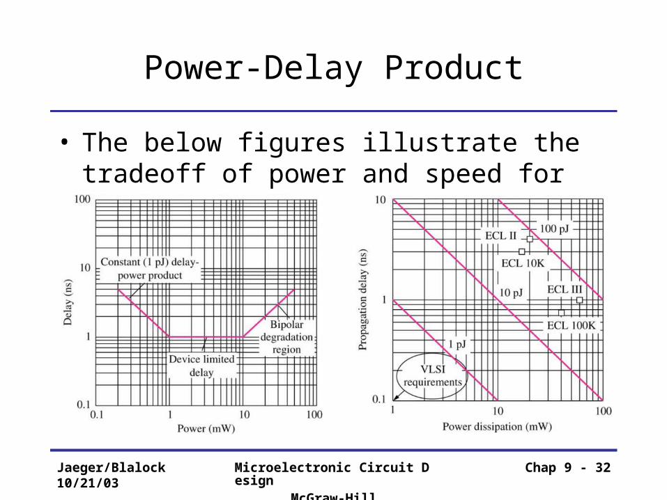
Power-Delay Product
• The below figures illustrate the tradeoff of power and speed for ECL gates
Jaeger/Blalock10/21/03
Microelectronic Circuit DesignMcGraw-Hill
Chap 9 - 33
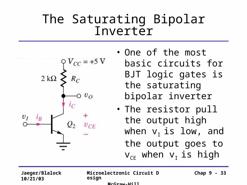
The Saturating Bipolar Inverter
• One of the most basic circuits for BJT logic gates is the saturating bipolar inverter
• The resistor pull the output high when vI is low, and the output goes to vCE when vI is high
Jaeger/Blalock10/21/03
Microelectronic Circuit DesignMcGraw-Hill
Chap 9 - 34
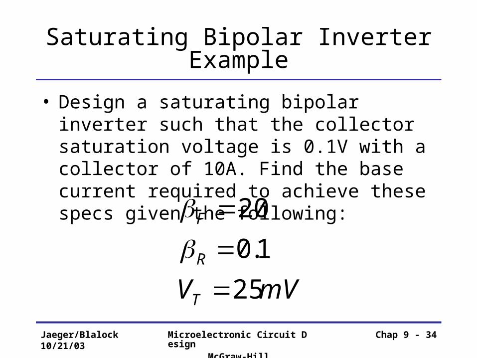
Saturating Bipolar Inverter Example
• Design a saturating bipolar inverter such that the collector saturation voltage is 0.1V with a collector of 10A. Find the base current required to achieve these specs given the following:
mVVT
R
F
25
1.0
20
Jaeger/Blalock10/21/03
Microelectronic Circuit DesignMcGraw-Hill
Chap 9 - 35
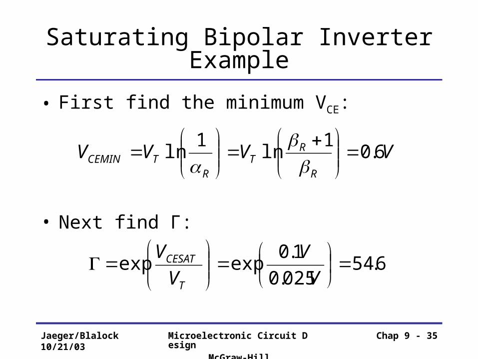
Saturating Bipolar Inverter Example
• First find the minimum VCE:
• Next find Г:
VVVVR
RT
RTCEMIN 6.0
1ln
1ln
6.54025.0
1.0expexp
V
V
V
V
T
CESAT
Jaeger/Blalock10/21/03
Microelectronic Circuit DesignMcGraw-Hill
Chap 9 - 36
Saturating Bipolar Inverter Example
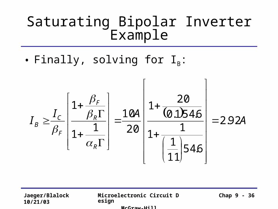
• Finally, solving for IB:
A
AII
R
R
F
F
CB 92.2
6.54111
11
6.541.020
1
20
101
1
1
Jaeger/Blalock10/21/03
Microelectronic Circuit DesignMcGraw-Hill
Chap 9 - 37
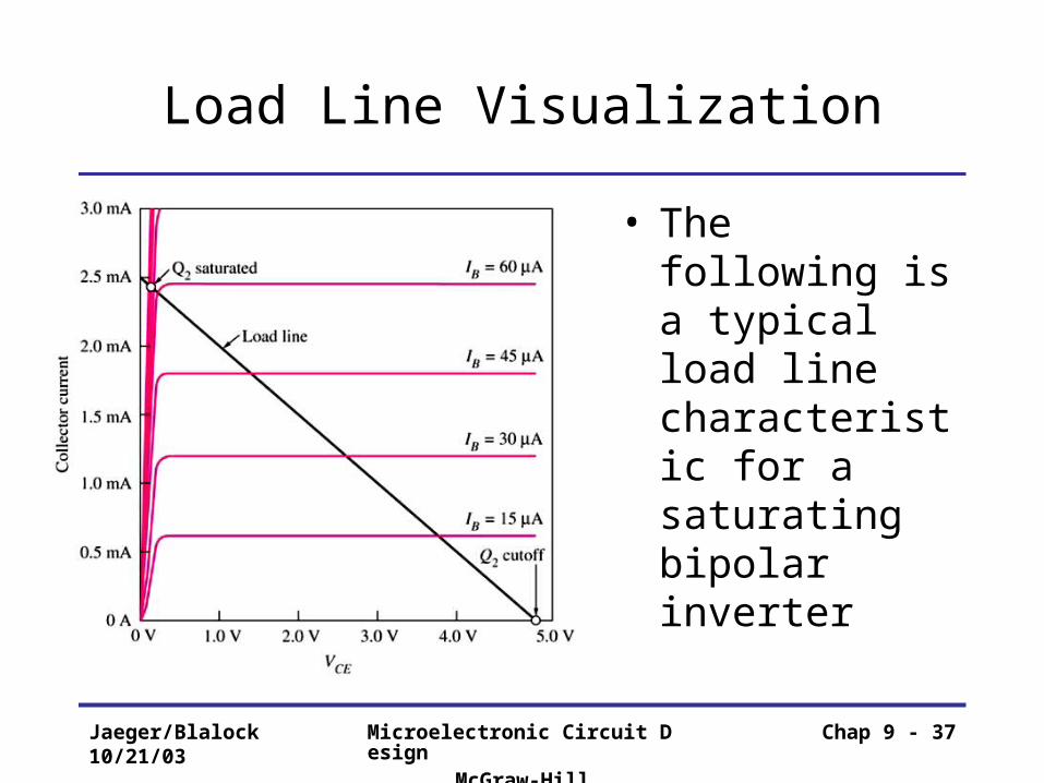
Load Line Visualization
• The following is a typical load line characteristic for a saturating bipolar inverter
Jaeger/Blalock10/21/03
Microelectronic Circuit DesignMcGraw-Hill
Chap 9 - 38
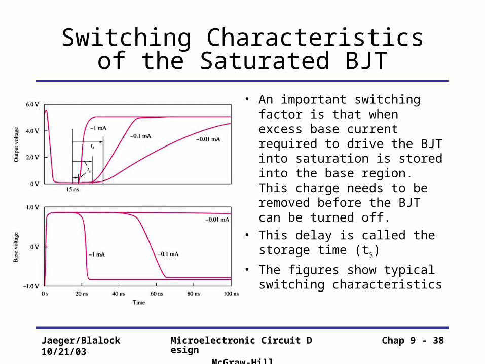
Switching Characteristics of the Saturated BJT
• An important switching factor is that when excess base current required to drive the BJT into saturation is stored into the base region. This charge needs to be removed before the BJT can be turned off.
• This delay is called the storage time (tS)
• The figures show typical switching characteristics
Jaeger/Blalock10/21/03
Microelectronic Circuit DesignMcGraw-Hill
Chap 9 - 39
Switching Characteristics of the Saturated BJT
• The storage time delays can be calculated using the following expressions:
• Where αF and αR are the forward and reverse common-base current gains, and τF and τR are the forward and reverse transit times
FR
RRFFS
BRF
CMAX
BRBFSS
Ii
IIt
1
ln
Jaeger/Blalock10/21/03
Microelectronic Circuit DesignMcGraw-Hill
Chap 9 - 40
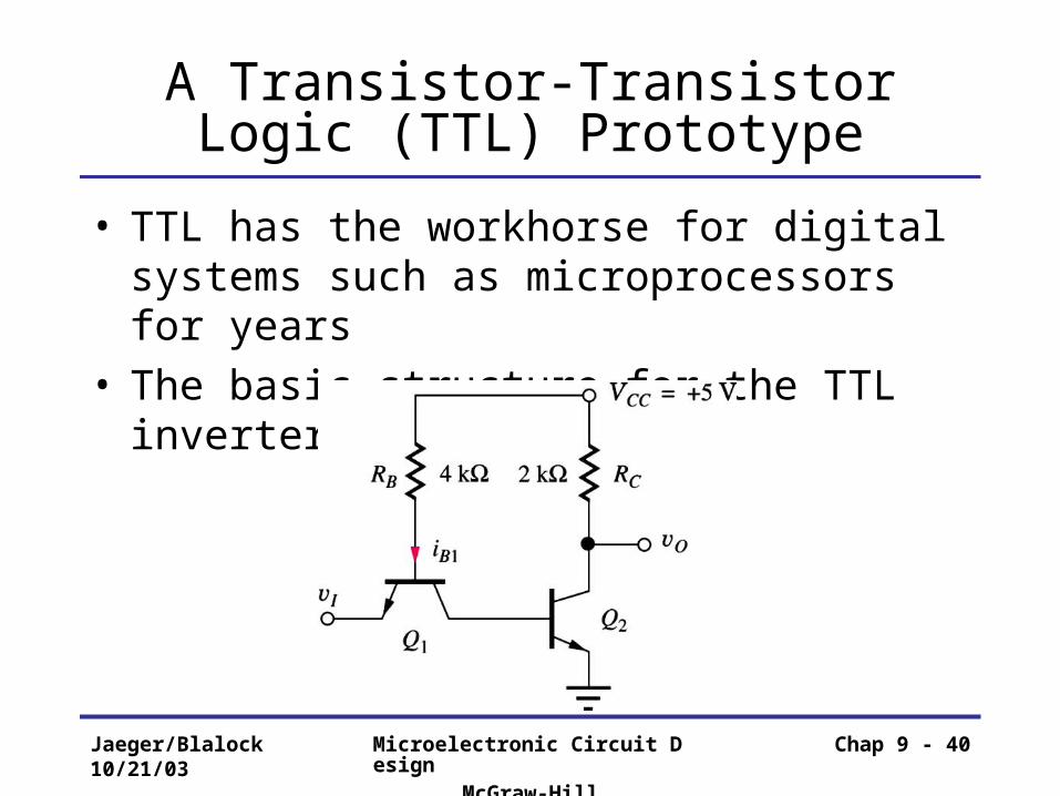
A Transistor-Transistor Logic (TTL) Prototype
• TTL has the workhorse for digital systems such as microprocessors for years
• The basic structure for the TTL inverter is shown below
Jaeger/Blalock10/21/03
Microelectronic Circuit DesignMcGraw-Hill
Chap 9 - 41
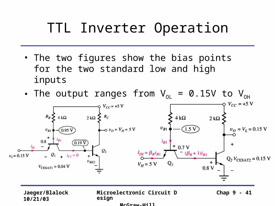
TTL Inverter Operation
• The two figures show the bias points for the two standard low and high inputs
• The output ranges from VOL = 0.15V to VOH = 5V
Jaeger/Blalock10/21/03
Microelectronic Circuit DesignMcGraw-Hill
Chap 9 - 42
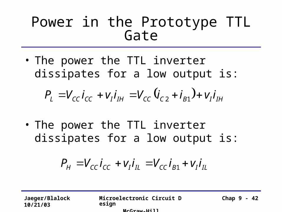
Power in the Prototype TTL Gate
• The power the TTL inverter dissipates for a low output is:
• The power the TTL inverter dissipates for a low output is:
IHIBCCCIHICCCCL iviiViviVP 12
ILIBCCILICCCCH iviViviVP 1
Jaeger/Blalock10/21/03
Microelectronic Circuit DesignMcGraw-Hill
Chap 9 - 43
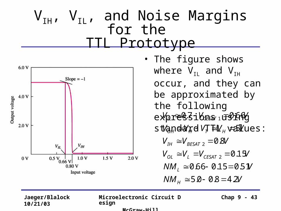
VIH, VIL, and Noise Margins for the TTL Prototype
• The figure shows where VIL and VIH occur, and they can be approximated by the following expressions using standard TTL values:
VNM
VNM
VVVV
VVV
VVVVV
VVV
H
L
CESATLOL
BESATIH
HTHOH
CESATIL
2.48.00.5
51.015.066.0
15.0
8.0
5
66.07.0
2
2
1
Jaeger/Blalock10/21/03
Microelectronic Circuit DesignMcGraw-Hill
Chap 9 - 44
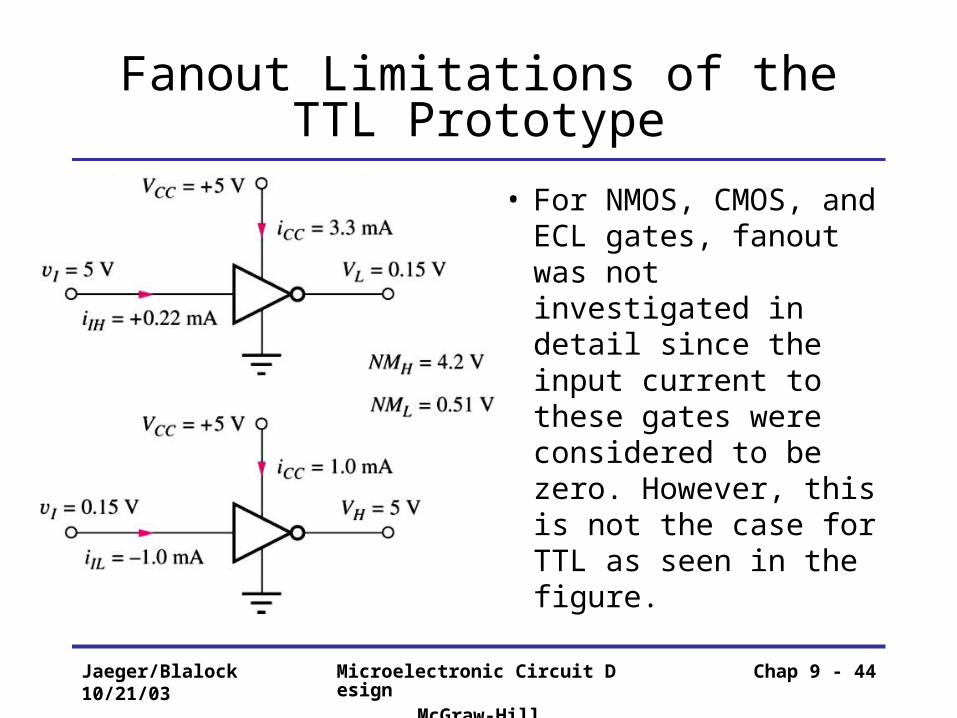
Fanout Limitations of the TTL Prototype
• For NMOS, CMOS, and ECL gates, fanout was not investigated in detail since the input current to these gates were considered to be zero. However, this is not the case for TTL as seen in the figure.
Jaeger/Blalock10/21/03
Microelectronic Circuit DesignMcGraw-Hill
Chap 9 - 45
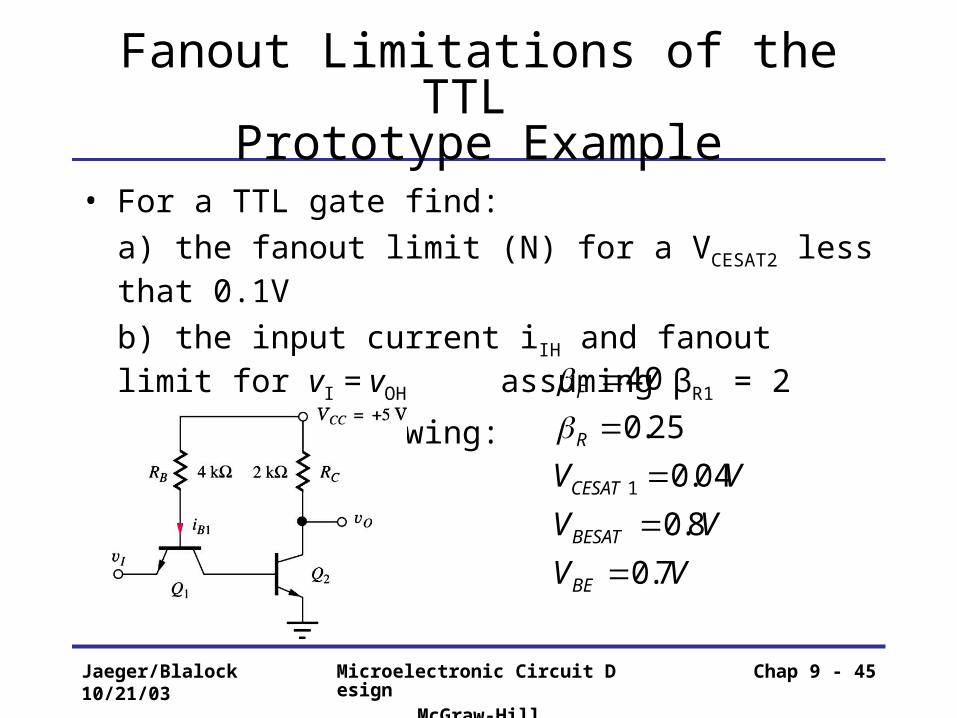
Fanout Limitations of the TTL Prototype Example
• For a TTL gate find:
a) the fanout limit (N) for a VCESAT2 less that 0.1V
b) the input current iIH and fanout limit for vI = vOH assuming βR1 = 2
Given the following:
VV
VV
VV
BE
BESAT
CESAT
R
F
7.0
8.0
04.0
25.0
40
1
Jaeger/Blalock10/21/03
Microelectronic Circuit DesignMcGraw-Hill
Chap 9 - 46
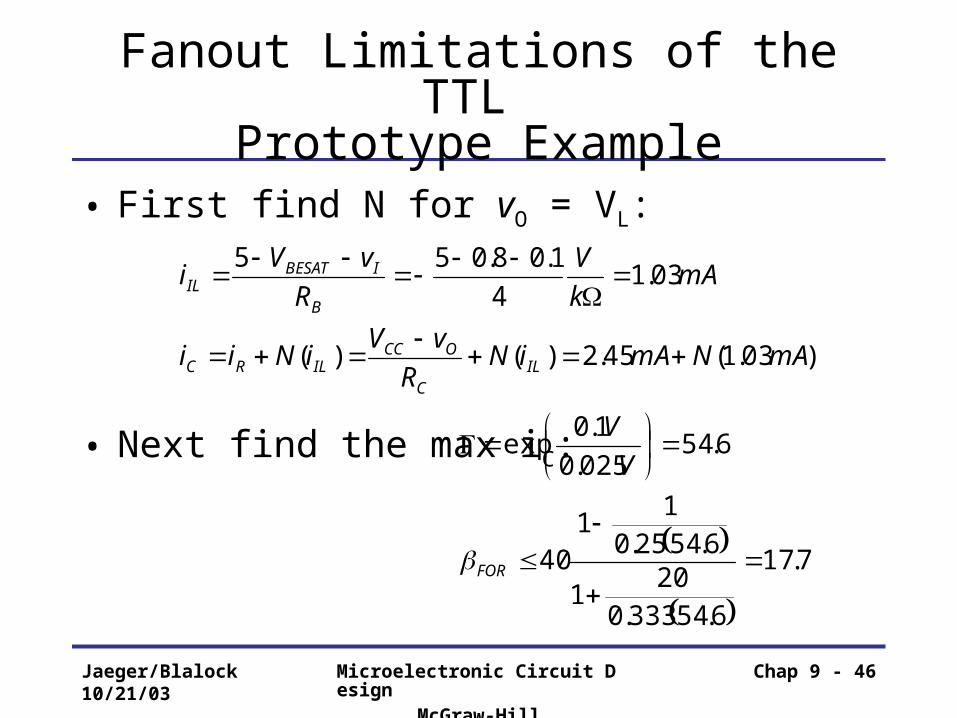
Fanout Limitations of the TTL Prototype Example
• First find N for vO = VL:
• Next find the max iC:
)03.1(45.2)()(
03.14
1.08.055
mANmAiNR
vViNii
mAk
V
R
vVi
ILC
OCCILRC
B
IBESATIL
7.17
6.54333.020
1
6.5425.01
140
6.54025.0
1.0exp
FOR
V
V
Jaeger/Blalock10/21/03
Microelectronic Circuit DesignMcGraw-Hill
Chap 9 - 47
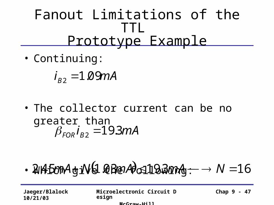
Fanout Limitations of the TTL Prototype Example
• Continuing:
• The collector current can be no greater than
• Which give the following:
mAi
mAi
BFOR
B
3.19
09.1
2
2
163.1903.145.2 NmAmANmA
Jaeger/Blalock10/21/03
Microelectronic Circuit DesignMcGraw-Hill
Chap 9 - 48
Fanout Limitations of the TTL Prototype Example
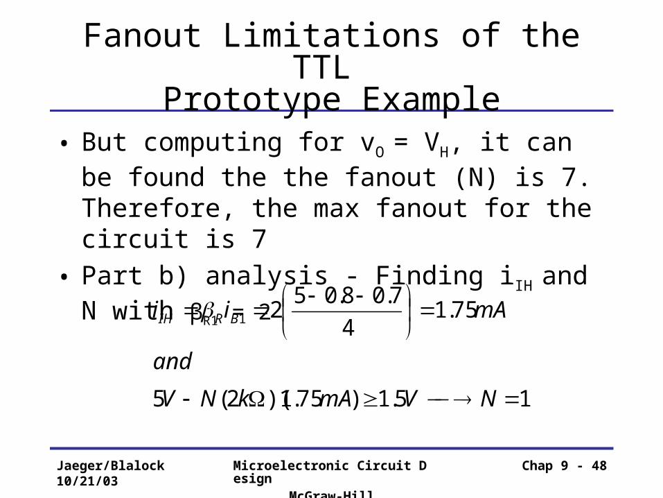
• But computing for vO = VH, it can be found the the fanout (N) is 7. Therefore, the max fanout for the circuit is 7
• Part b) analysis - Finding iIH and N with βR1 = 2
15.1)75.1)(2(5
75.14
7.08.0521
NVmAkNV
and
mAii BRIH
Jaeger/Blalock10/21/03
Microelectronic Circuit DesignMcGraw-Hill
Chap 9 - 49
The Standard 7400 Series TTL Inverter
• One problem of the TTL inverter prototype described so far is that the dynamic response is asymmetrical due to the use of a resistive load to pull the output up and a BJT to pull the output down
• Another problem is that the fanout capability is highly sensitive to βR
Jaeger/Blalock10/21/03
Microelectronic Circuit DesignMcGraw-Hill
Chap 9 - 50
The Standard 7400 Series TTL Inverter
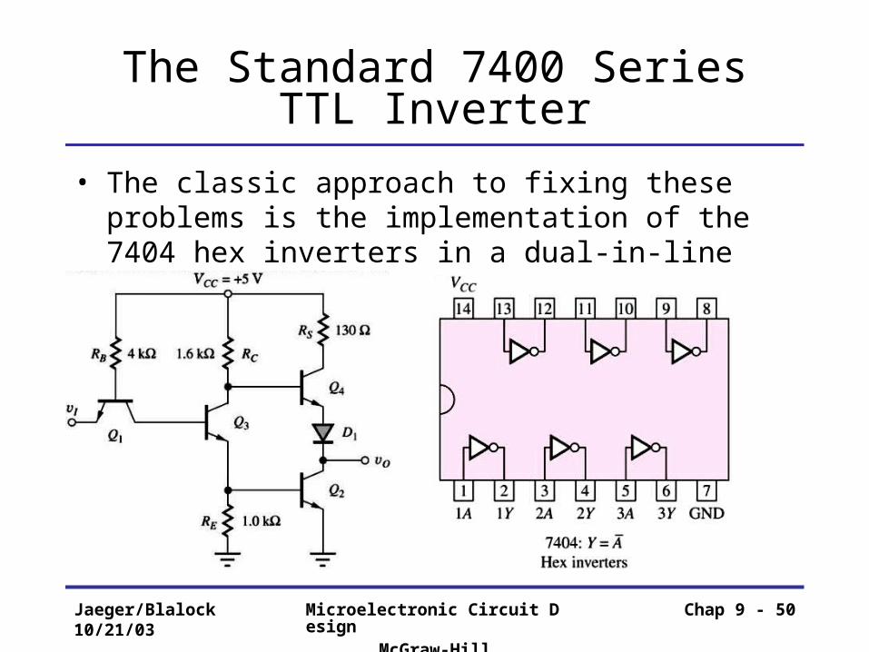
• The classic approach to fixing these problems is the implementation of the 7404 hex inverters in a dual-in-line package (DIP)
Jaeger/Blalock10/21/03
Microelectronic Circuit DesignMcGraw-Hill
Chap 9 - 51
The Standard 7400 Series TTL Inverter
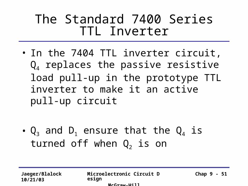
• In the 7404 TTL inverter circuit, Q4 replaces the passive resistive load pull-up in the prototype TTL inverter to make it an active pull-up circuit
• Q3 and D1 ensure that the Q4 is turned off when Q2 is on
Jaeger/Blalock10/21/03
Microelectronic Circuit DesignMcGraw-Hill
Chap 9 - 52
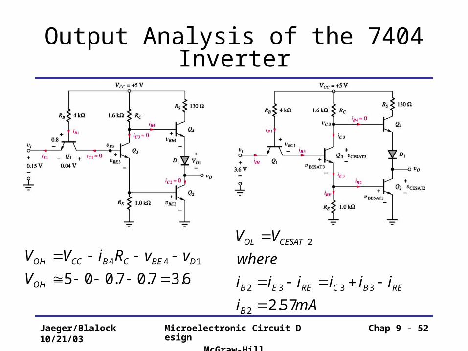
Output Analysis of the 7404 Inverter
6.37.07.005144
OH
DBECBCCOH
V
vvRiVV
mAi
iiiiii
where
VV
B
REBCREEB
CESATOL
57.22
3332
2
Jaeger/Blalock10/21/03
Microelectronic Circuit DesignMcGraw-Hill
Chap 9 - 53
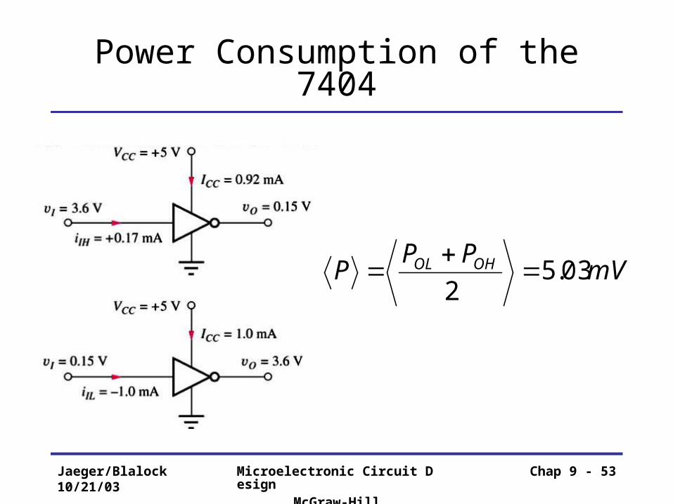
Power Consumption of the 7404
mVPP
P OHOL 03.52
Jaeger/Blalock10/21/03
Microelectronic Circuit DesignMcGraw-Hill
Chap 9 - 54
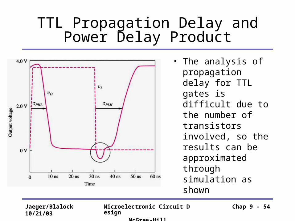
TTL Propagation Delay and Power Delay Product
• The analysis of propagation delay for TTL gates is difficult due to the number of transistors involved, so the results can be approximated through simulation as shown
Jaeger/Blalock10/21/03
Microelectronic Circuit DesignMcGraw-Hill
Chap 9 - 55
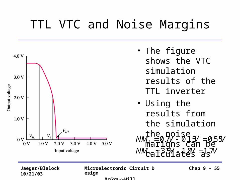
TTL VTC and Noise Margins
• The figure shows the VTC simulation results of the TTL inverter
• Using the results from the simulation the noise marigns can be calculates as
VVVNM
VVVNM
H
L
7.18.15.3
55.015.07.0
Jaeger/Blalock10/21/03
Microelectronic Circuit DesignMcGraw-Hill
Chap 9 - 56
Fanout Limitations of Standard TTL
• The active pull drastically improves the fanout capabilities of the TTL inverter
• However, due to process variations, and the requirement for the device to operate over a range of temperatures, N is specified to be less than 10
7.72
)57.2(3.28)1(2
N
mAmAN
iNi BFORIL
Jaeger/Blalock10/21/03
Microelectronic Circuit DesignMcGraw-Hill
Chap 9 - 57
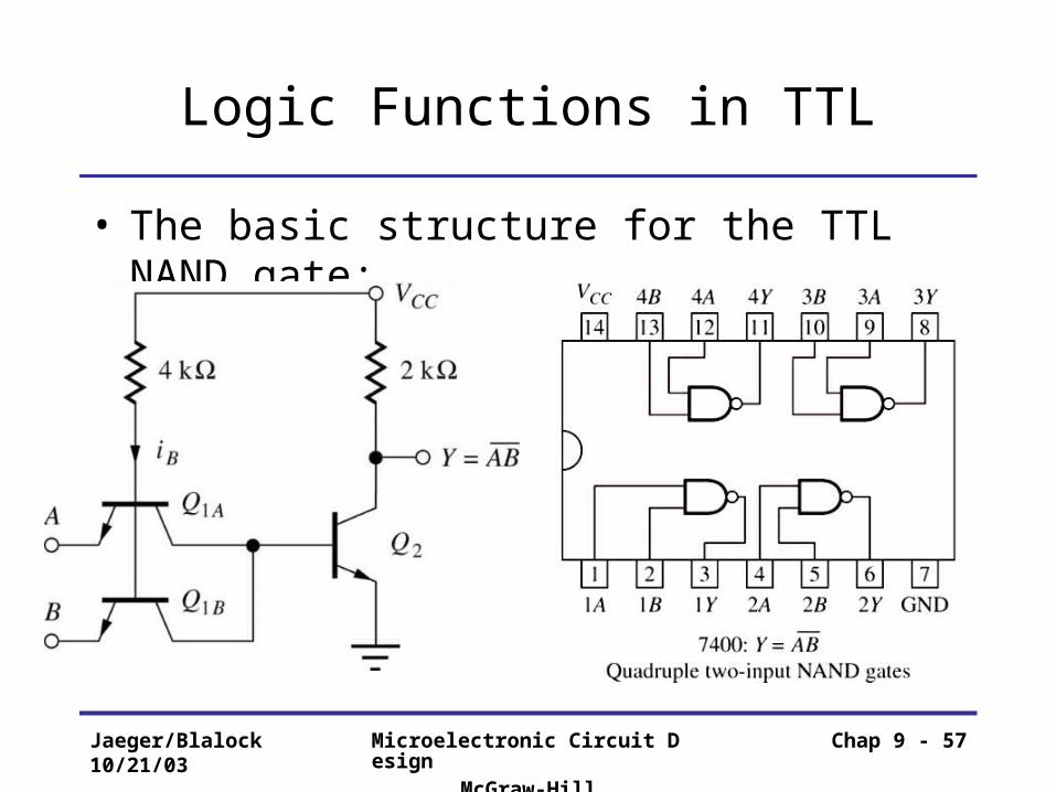
Logic Functions in TTL
• The basic structure for the TTL NAND gate:
Jaeger/Blalock10/21/03
Microelectronic Circuit DesignMcGraw-Hill
Chap 9 - 58
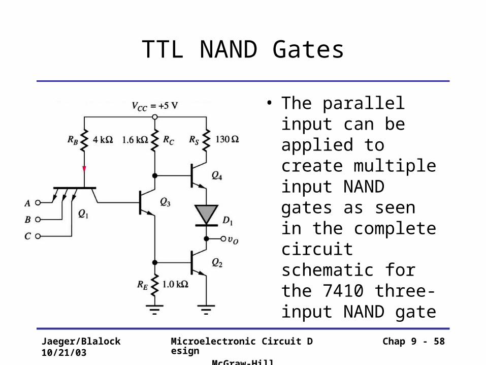
TTL NAND Gates
• The parallel input can be applied to create multiple input NAND gates as seen in the complete circuit schematic for the 7410 three-input NAND gate
Jaeger/Blalock10/21/03
Microelectronic Circuit DesignMcGraw-Hill
Chap 9 - 59
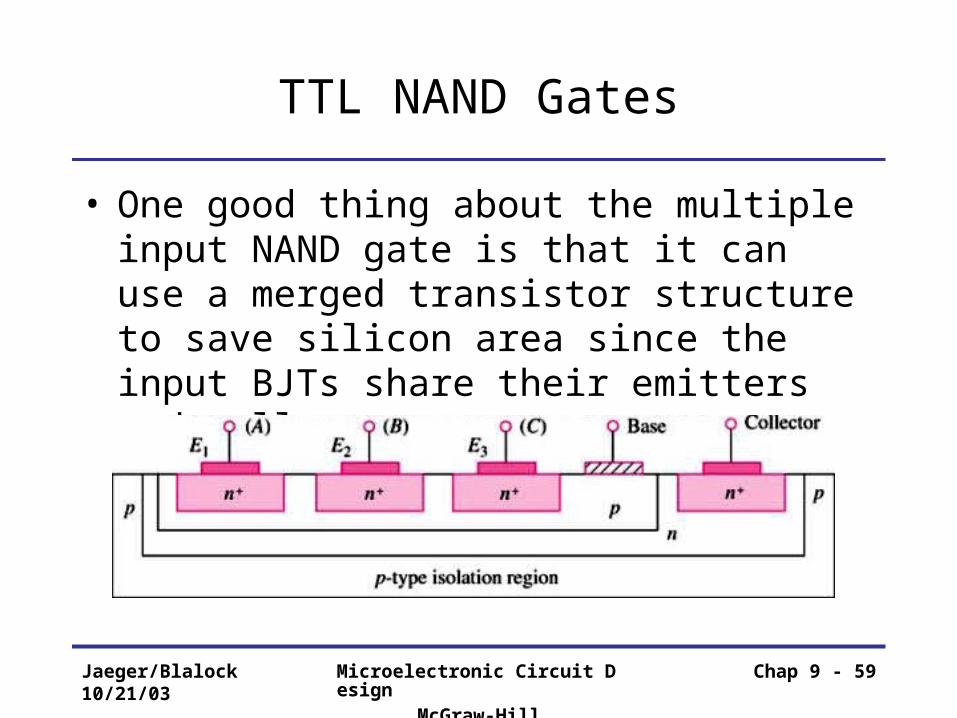
TTL NAND Gates
• One good thing about the multiple input NAND gate is that it can use a merged transistor structure to save silicon area since the input BJTs share their emitters and collectors
Jaeger/Blalock10/21/03
Microelectronic Circuit DesignMcGraw-Hill
Chap 9 - 60
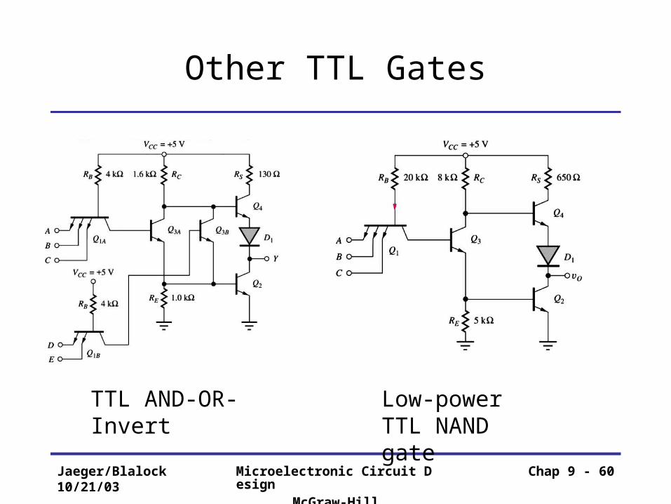
Other TTL Gates
TTL AND-OR-Invert
Low-power TTL NAND gate
Jaeger/Blalock10/21/03
Microelectronic Circuit DesignMcGraw-Hill
Chap 9 - 61
Input Clamping Diodes for TTL
• From a transient simulation of the TTL inverter, a negative-going transient can be observed due to the fast input signal transition
• Another source of the transients is from the distributed L-C interconnection network between gates causing “ringing”
Jaeger/Blalock10/21/03
Microelectronic Circuit DesignMcGraw-Hill
Chap 9 - 62
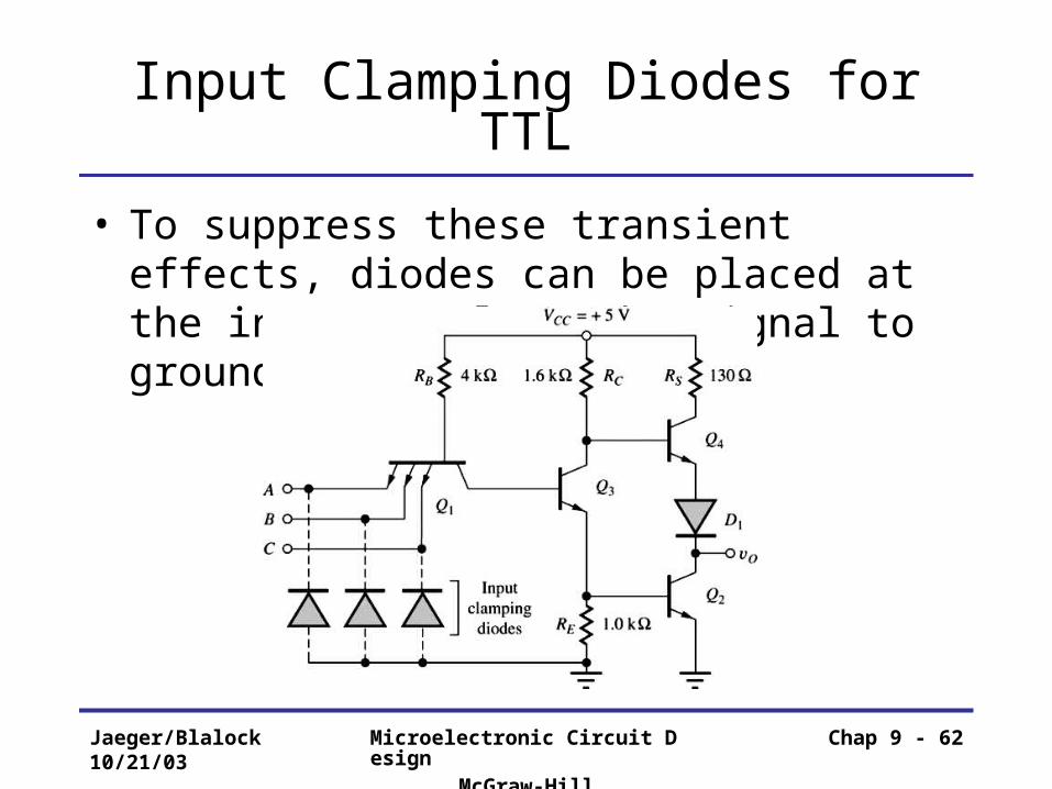
Input Clamping Diodes for TTL
• To suppress these transient effects, diodes can be placed at the input to clamp the signal to ground
Jaeger/Blalock10/21/03
Microelectronic Circuit DesignMcGraw-Hill
Chap 9 - 63
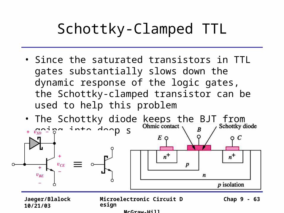
Schottky-Clamped TTL
• Since the saturated transistors in TTL gates substantially slows down the dynamic response of the logic gates, the Schottky-clamped transistor can be used to help this problem
• The Schottky diode keeps the BJT from going into deep saturation
Jaeger/Blalock10/21/03
Microelectronic Circuit DesignMcGraw-Hill
Chap 9 - 64
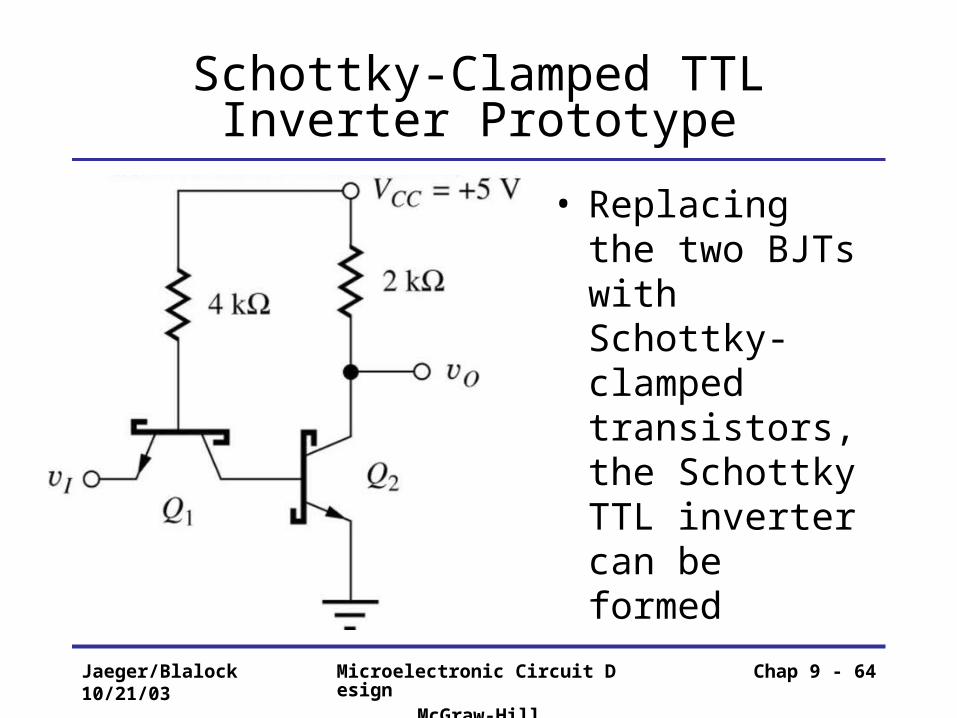
Schottky-Clamped TTL Inverter Prototype
• Replacing the two BJTs with Schottky-clamped transistors, the Schottky TTL inverter can be formed
Jaeger/Blalock10/21/03
Microelectronic Circuit DesignMcGraw-Hill
Chap 9 - 65
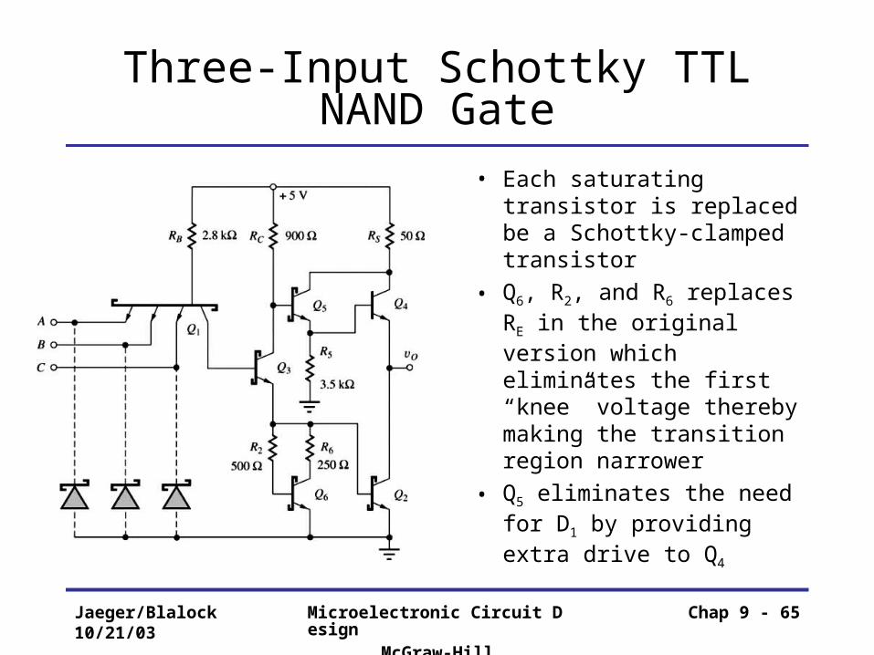
Three-Input Schottky TTL NAND Gate
• Each saturating transistor is replaced be a Schottky-clamped transistor
• Q6, R2, and R6 replaces RE in the original version which eliminates the first “knee” voltage thereby making the transition region narrower
• Q5 eliminates the need for D1 by providing extra drive to Q4
Jaeger/Blalock10/21/03
Microelectronic Circuit DesignMcGraw-Hill
Chap 9 - 66
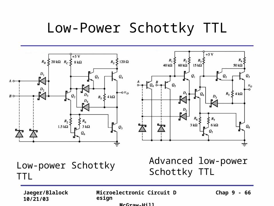
Low-Power Schottky TTL
Low-power Schottky TTL Advanced low-power Schottky TTL
Jaeger/Blalock10/21/03
Microelectronic Circuit DesignMcGraw-Hill
Chap 9 - 67
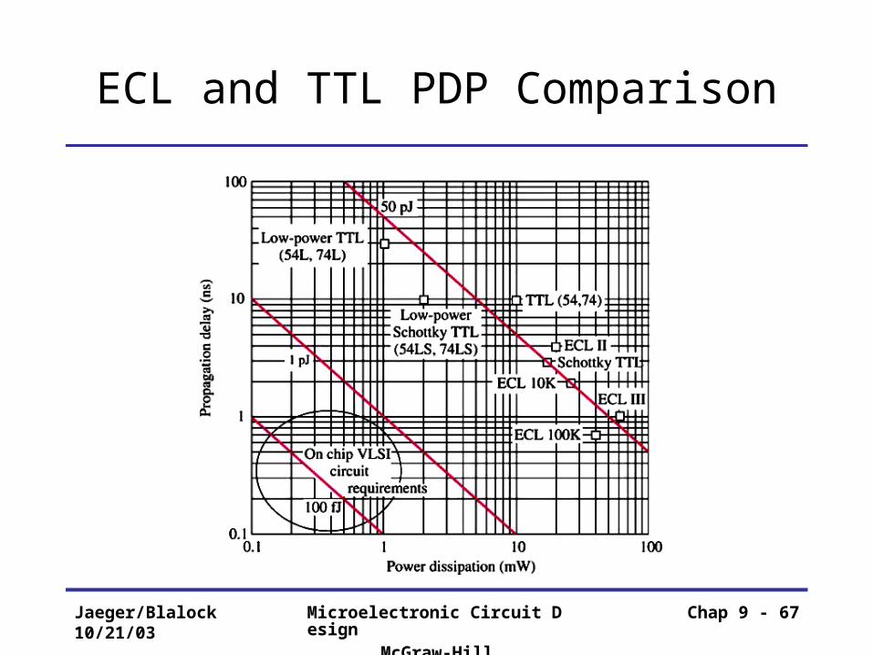
ECL and TTL PDP Comparison
Jaeger/Blalock10/21/03
Microelectronic Circuit DesignMcGraw-Hill
Chap 9 - 68
BiCMOS Logic
• BiCMOS is a complex processing technology that provides both NMOS and PMOS, as well as npn and pnp bipolars
• The high impedance input of logic gates (does not require much to drive them) are provided from the MOSFETs and high current drive can be provided from the BJTs due to their high current gain and transconductance
Jaeger/Blalock10/21/03
Microelectronic Circuit DesignMcGraw-Hill
Chap 9 - 69
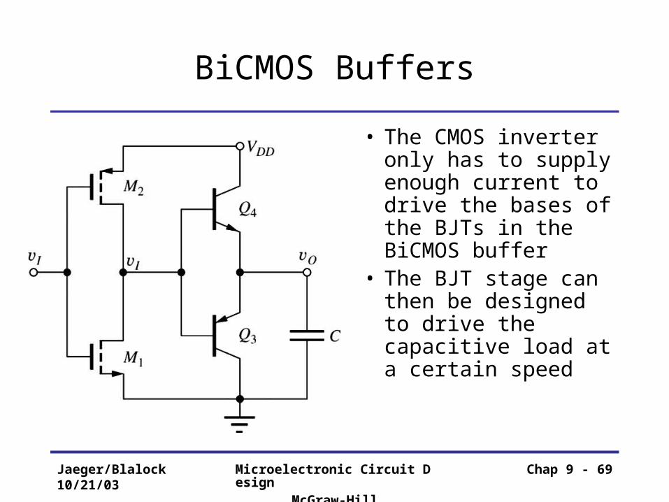
BiCMOS Buffers
• The CMOS inverter only has to supply enough current to drive the bases of the BJTs in the BiCMOS buffer
• The BJT stage can then be designed to drive the capacitive load at a certain speed
Jaeger/Blalock10/21/03
Microelectronic Circuit DesignMcGraw-Hill
Chap 9 - 70
BiCMOS Buffers
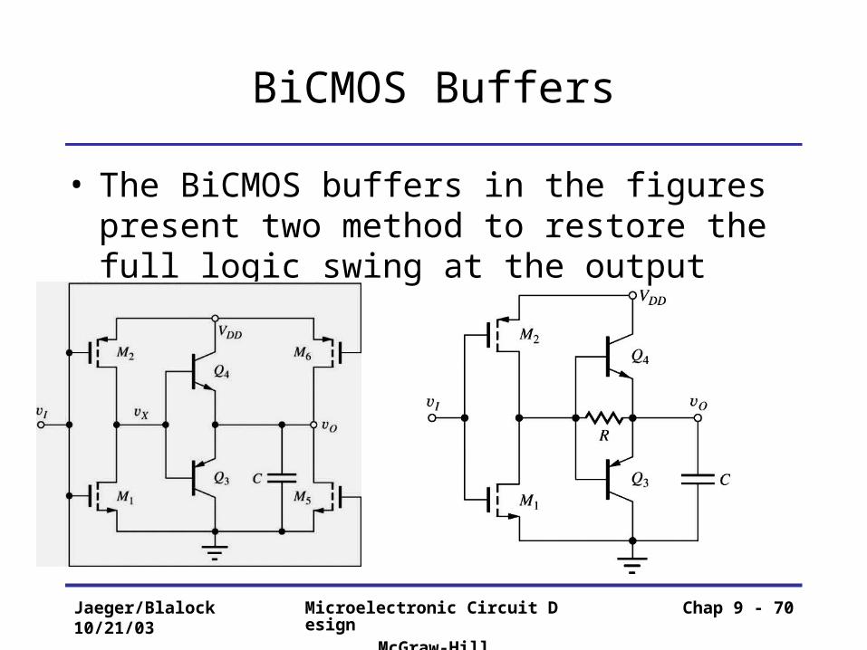
• The BiCMOS buffers in the figures present two method to restore the full logic swing at the output
Jaeger/Blalock10/21/03
Microelectronic Circuit DesignMcGraw-Hill
Chap 9 - 71
BiNMOS Buffer
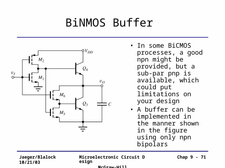
• In some BiCMOS processes, a good npn might be provided, but a sub-par pnp is available, which could put limitations on your design
• A buffer can be implemented in the manner shown in the figure using only npn bipolars
Jaeger/Blalock10/21/03
Microelectronic Circuit DesignMcGraw-Hill
Chap 9 - 72
Other BiNMOS Circuits
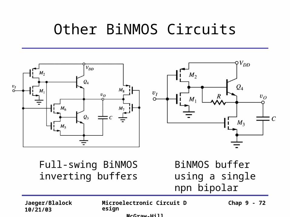
Full-swing BiNMOS inverting buffers
BiNMOS buffer using a single npn bipolar
Jaeger/Blalock10/21/03
Microelectronic Circuit DesignMcGraw-Hill
Chap 9 - 73
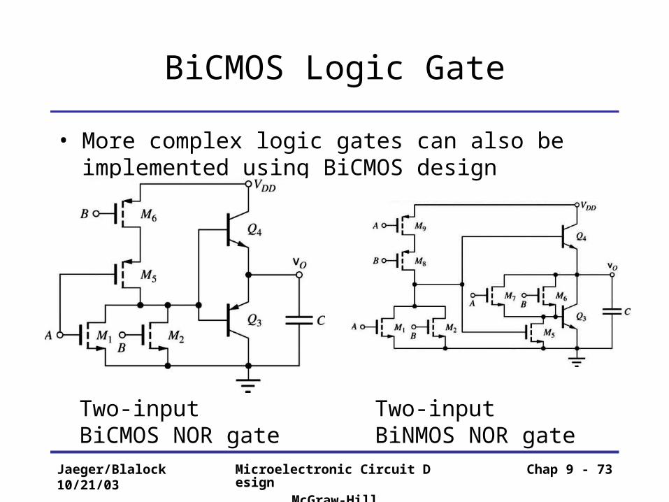
BiCMOS Logic Gate
• More complex logic gates can also be implemented using BiCMOS design
Two-input BiCMOS NOR gate
Two-input BiNMOS NOR gate
Jaeger/Blalock10/21/03
Microelectronic Circuit DesignMcGraw-Hill
Chap 9 - 74
End of Chapter 9


