- 441 -
Chapter 16
Oscillator Circuits and Applications _____________________________________________ 16.0 Introduction Oscillator contains circuit that generates an output signal without necessity of an input signal. It is a circuit that produces a repetitive waveform on its output with only dc supply as input. The oscillator can be sinusoidal or non-sinusoidal type. They can be used in many applications such as communication and digital system.
Oscillator operation is based on positive feedback whereby portion β of the output signal Vout is feedback without phase φ change. This shall mean that there is no phase difference between the input and feedback signal.
Many oscillator circuits can be designed using operational amplifier circuit. It can generate various types of waveform with no input other than dc supply. These are known as signal generators or oscillators.
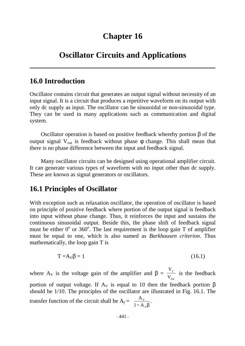
16.1 Principles of Oscillator With exception such as relaxation oscillator, the operation of oscillator is based on principle of positive feedback where portion of the output signal is feedback into input without phase change. Thus, it reinforces the input and sustains the continuous sinusoidal output. Beside this, the phase shift of feedback signal must be either 0o or 360o. The last requirement is the loop gain T of amplifier must be equal to one, which is also named as Barkhausen criterion. Thus mathematically, the loop gain T is
T =AVβ = 1 (16.1)
where AV is the voltage gain of the amplifier and β = V
Vout
f is the feedback
portion of output voltage. If AV is equal to 10 then the feedback portion β should be 1/10. The principles of the oscillator are illustrated in Fig. 16.1. The
transfer function of the circuit shall be Af = β− V
V
A1
A.
16 Oscillator Circuits and Applications
- 442 -
Figure 16.1: Principle of sinusoidal oscillator
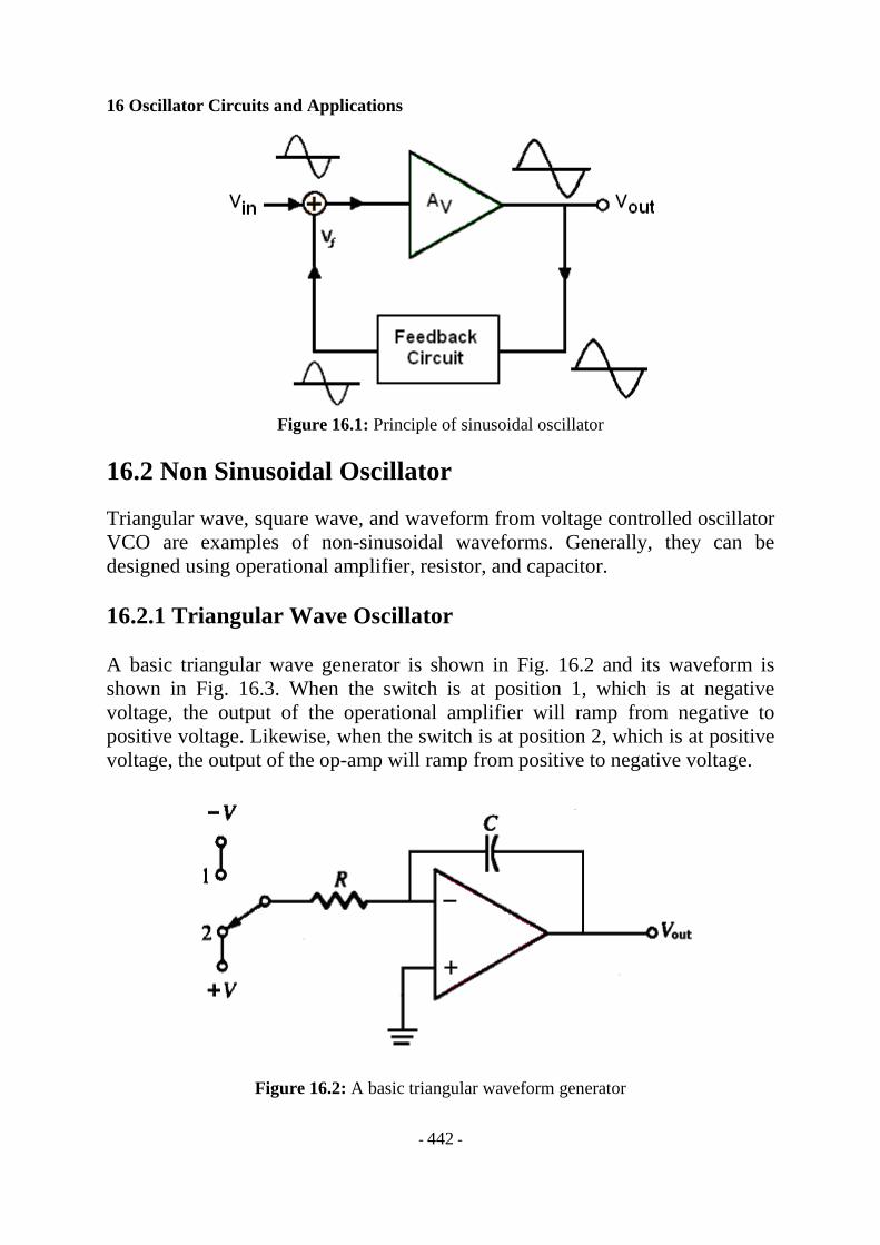
16.2 Non Sinusoidal Oscillator Triangular wave, square wave, and waveform from voltage controlled oscillator VCO are examples of non-sinusoidal waveforms. Generally, they can be designed using operational amplifier, resistor, and capacitor. 16.2.1 Triangular Wave Oscillator A basic triangular wave generator is shown in Fig. 16.2 and its waveform is shown in Fig. 16.3. When the switch is at position 1, which is at negative voltage, the output of the operational amplifier will ramp from negative to positive voltage. Likewise, when the switch is at position 2, which is at positive voltage, the output of the op-amp will ramp from positive to negative voltage.
Figure 16.2: A basic triangular waveform generator
16 Oscillator Circuits and Applications
- 443 -
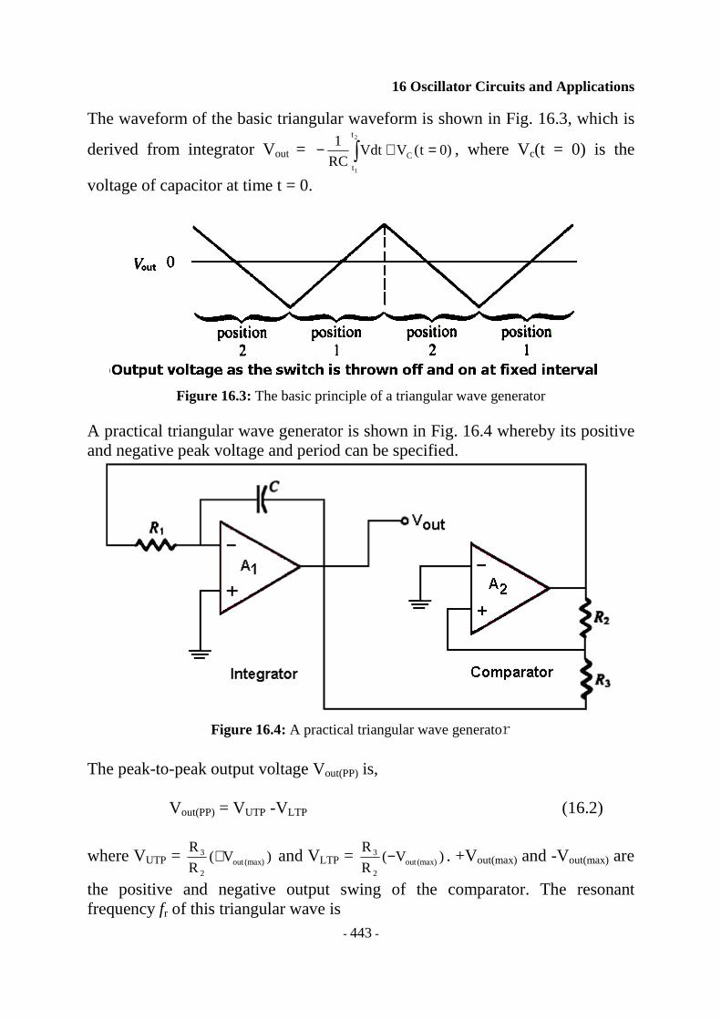
The waveform of the basic triangular waveform is shown in Fig. 16.3, which is
derived from integrator Vout = )0t(VVdtRC
1C
t
t
2
1
=+− ∫ , where Vc(t = 0) is the
voltage of capacitor at time t = 0.
Figure 16.3: The basic principle of a triangular wave generator
A practical triangular wave generator is shown in Fig. 16.4 whereby its positive and negative peak voltage and period can be specified.
Figure 16.4: A practical triangular wave generator The peak-to-peak output voltage Vout(PP) is, Vout(PP) = VUTP -VLTP (16.2)
where VUTP = )V(R
R(max)out
2
3 + and VLTP = )V(R
R(max)out
2
3 − . +Vout(max) and -Vout(max) are
the positive and negative output swing of the comparator. The resonant frequency fr of this triangular wave is
16 Oscillator Circuits and Applications
- 444 -
fr =
⋅
3
2
1 R
R
CR4
1 (16.3)
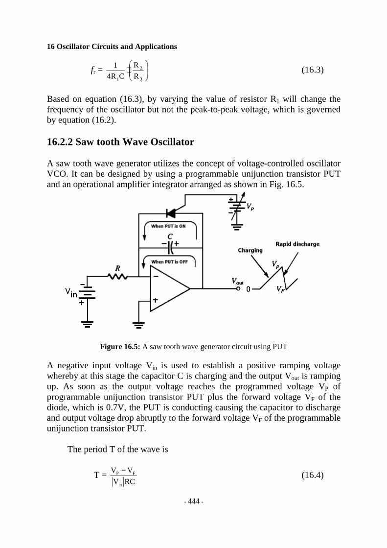
Based on equation (16.3), by varying the value of resistor R1 will change the frequency of the oscillator but not the peak-to-peak voltage, which is governed by equation (16.2). 16.2.2 Saw tooth Wave Oscillator A saw tooth wave generator utilizes the concept of voltage-controlled oscillator VCO. It can be designed by using a programmable unijunction transistor PUT and an operational amplifier integrator arranged as shown in Fig. 16.5.
Figure 16.5: A saw tooth wave generator circuit using PUT
A negative input voltage Vin is used to establish a positive ramping voltage whereby at this stage the capacitor C is charging and the output Vout is ramping up. As soon as the output voltage reaches the programmed voltage VP of programmable unijunction transistor PUT plus the forward voltage VF of the diode, which is 0.7V, the PUT is conducting causing the capacitor to discharge and output voltage drop abruptly to the forward voltage VF of the programmable unijunction transistor PUT.
The period T of the wave is
T = RCV
VV
in
FP − (16.4)
16 Oscillator Circuits and Applications
- 445 -
where |Vin|RC is ramping rate of output voltage.
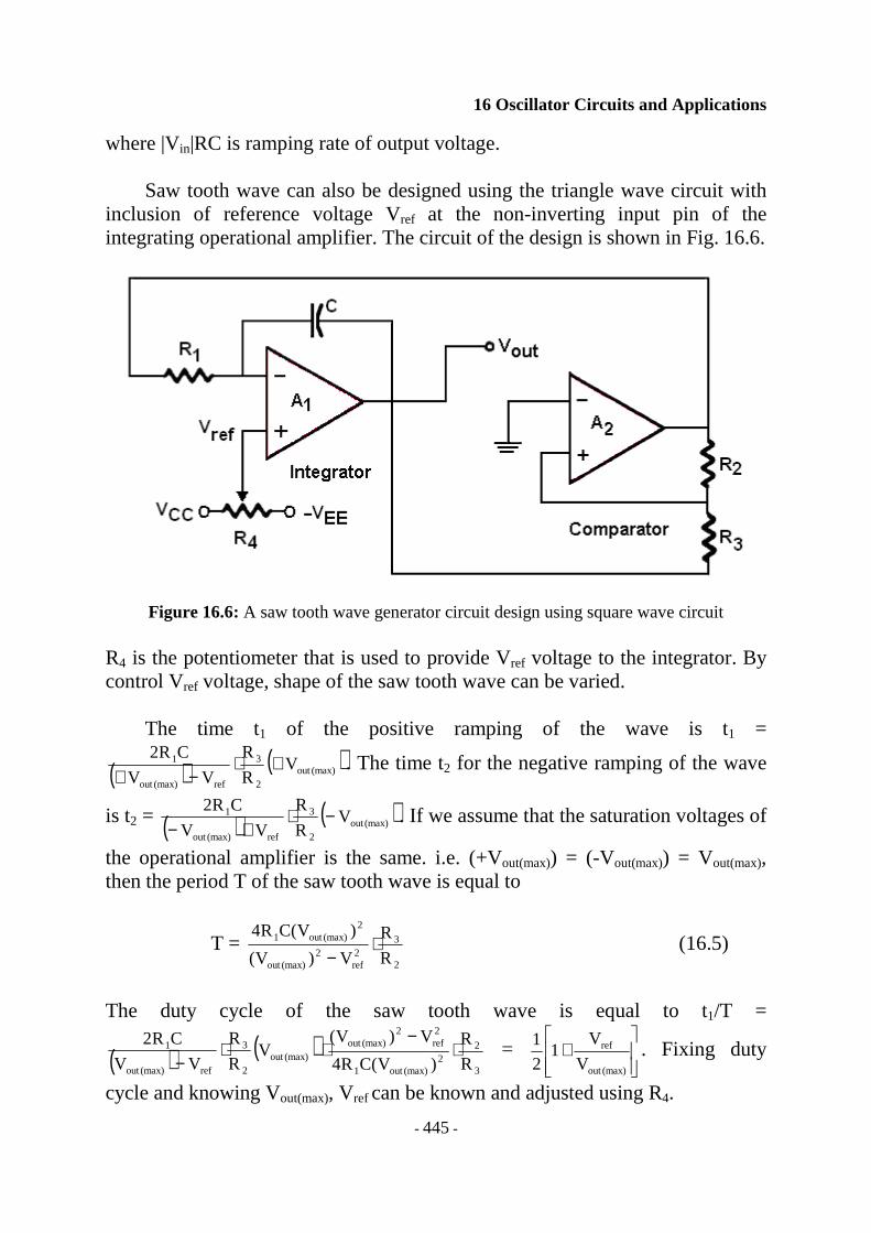
Saw tooth wave can also be designed using the triangle wave circuit with inclusion of reference voltage Vref at the non-inverting input pin of the integrating operational amplifier. The circuit of the design is shown in Fig. 16.6.
Figure 16.6: A saw tooth wave generator circuit design using square wave circuit R4 is the potentiometer that is used to provide Vref voltage to the integrator. By control Vref voltage, shape of the saw tooth wave can be varied.
The time t1 of the positive ramping of the wave is t1 =
( ) ( )(max)out2
3
ref(max)out
1 VR
R
VV
CR2+⋅
−+. The time t2 for the negative ramping of the wave
is t2 = ( ) ( )(max)out2
3
ref(max)out
1 VR
R
VV
CR2−⋅
+−. If we assume that the saturation voltages of
the operational amplifier is the same. i.e. (+Vout(max)) = (-Vout(max)) = Vout(max), then the period T of the saw tooth wave is equal to
T = 2
32ref
2(max)out
2(max)out1
R
R
V)V(
)V(CR4⋅
− (16.5)
The duty cycle of the saw tooth wave is equal to t1/T =
( ) ( )(max)out2
3
ref(max)out
1 VR
R
VV
CR2⋅
− 3
22
(max)out1
2ref
2(max)out
R
R
)V(CR4
V)V(⋅
−⋅ =
+
(max)out
ref
V
V1
2
1 . Fixing duty
cycle and knowing Vout(max), Vref can be known and adjusted using R4.
16 Oscillator Circuits and Applications
- 446 -
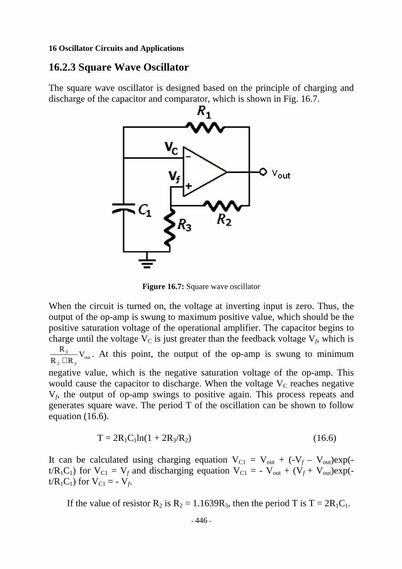
16.2.3 Square Wave Oscillator The square wave oscillator is designed based on the principle of charging and discharge of the capacitor and comparator, which is shown in Fig. 16.7.
Figure 16.7: Square wave oscillator
When the circuit is turned on, the voltage at inverting input is zero. Thus, the output of the op-amp is swung to maximum positive value, which should be the positive saturation voltage of the operational amplifier. The capacitor begins to charge until the voltage VC is just greater than the feedback voltage Vf, which is
out32
3 VRR
R
+. At this point, the output of the op-amp is swung to minimum
negative value, which is the negative saturation voltage of the op-amp. This would cause the capacitor to discharge. When the voltage VC reaches negative Vf, the output of op-amp swings to positive again. This process repeats and generates square wave. The period T of the oscillation can be shown to follow equation (16.6). T = 2R1C1ln(1 + 2R3/R2) (16.6) It can be calculated using charging equation VC1 = Vout + (-Vf – Vout)exp(-t/R1C1) for VC1 = Vf and discharging equation VC1 = - Vout + (Vf + Vout)exp(-t/R1C1) for VC1 = - Vf.
If the value of resistor R2 is R2 = 1.1639R3, then the period T is T = 2R1C1.
16 Oscillator Circuits and Applications
- 447 -
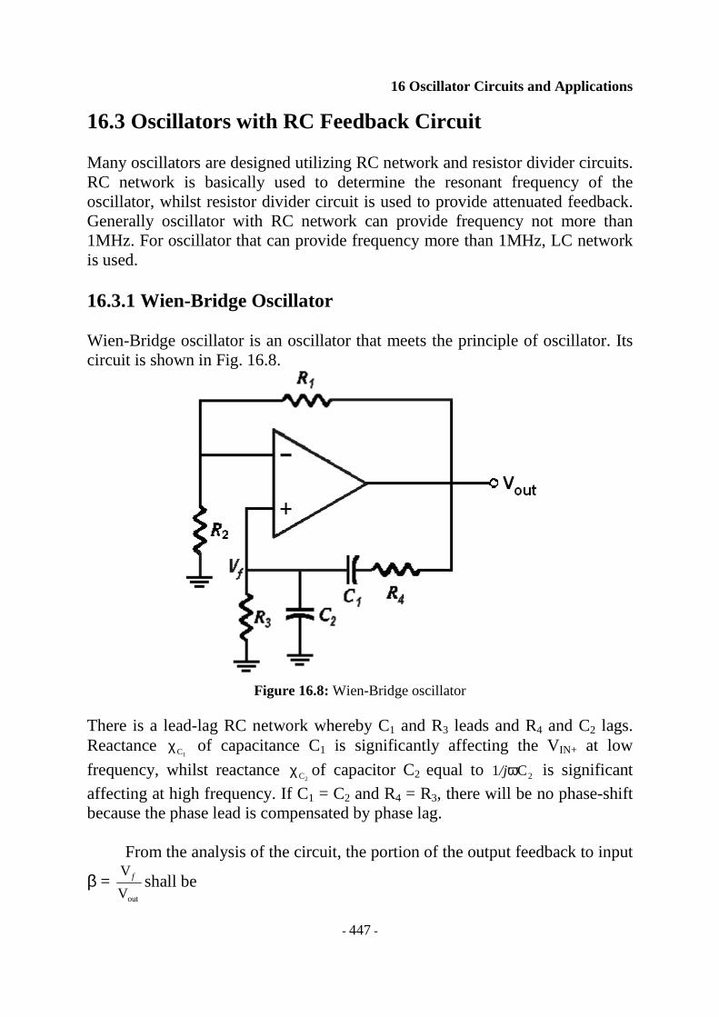
16.3 Oscillators with RC Feedback Circuit Many oscillators are designed utilizing RC network and resistor divider circuits. RC network is basically used to determine the resonant frequency of the oscillator, whilst resistor divider circuit is used to provide attenuated feedback. Generally oscillator with RC network can provide frequency not more than 1MHz. For oscillator that can provide frequency more than 1MHz, LC network is used. 16.3.1 Wien-Bridge Oscillator Wien-Bridge oscillator is an oscillator that meets the principle of oscillator. Its circuit is shown in Fig. 16.8.
Figure 16.8: Wien-Bridge oscillator
There is a lead-lag RC network whereby C1 and R3 leads and R4 and C2 lags. Reactance χC1
of capacitance C1 is significantly affecting the VIN+ at low
frequency, whilst reactance χC2of capacitor C2 equal to 2C1 ω/j is significant
affecting at high frequency. If C1 = C2 and R4 = R3, there will be no phase-shift because the phase lead is compensated by phase lag.
From the analysis of the circuit, the portion of the output feedback to input
β = outV
V f shall be
16 Oscillator Circuits and Applications
- 448 -
β = V
Vout
f = j
j
ωω ω
RC
RC R C3 1 2 2 2+ −( ) (16.7)
Applying Barkhausen principle of oscillator design this shall mean that overall
loop gain A =j
j
ωω ω
RC
RC R C3 1 2 2 2+ −( )AV = 1. From real part and imaginary part of
the complex number solution, the resonant frequency fr of the oscillator shall be
fr = RC2
1
π (16.8)
The voltage gain AV of the amplifier should be 3. This shall mean that feedback portion β is 1/3.
Since the voltage gain of the amplifier AV should be 3, this shall mean that
AV = 2
21
R
RR + = 3 (16.9)
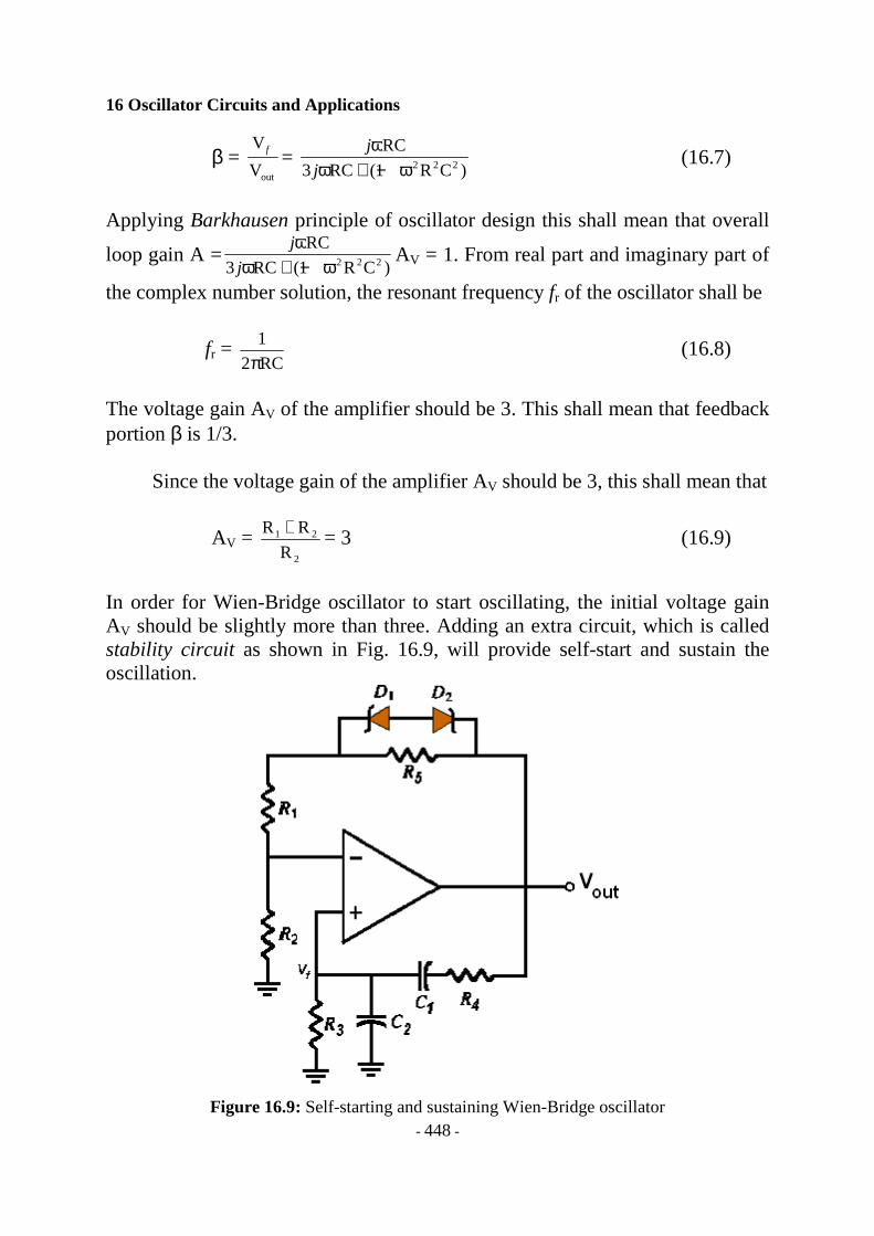
In order for Wien-Bridge oscillator to start oscillating, the initial voltage gain AV should be slightly more than three. Adding an extra circuit, which is called stability circuit as shown in Fig. 16.9, will provide self-start and sustain the oscillation.
Figure 16.9: Self-starting and sustaining Wien-Bridge oscillator
16 Oscillator Circuits and Applications
- 449 -
Before zener diode D1 and D2 conduct, the voltage gain AV of the amplifier is
AV = R R
R
R
R1 2
2
5
2
++ =
2
5
R
R3+ (16.10)
Thus, it meets the conditions of closed loop gain greater than 1 for self-starting of the oscillator.
When the output voltage reaches the zener breakdown voltage plus 0.7V, the zener diode conducts. Its forward resistance would be much smaller than the resistance value of resistor R5. Thus, the closed loop gain will be back to 1 and oscillation would be sustained. 16.3.2 Operational Amplifier Phase-Shift Oscillator The operational amplifier phase-shift oscillator is another oscillator type that meets the principles of oscillator design. Its circuit is shown in Fig. 16.10.
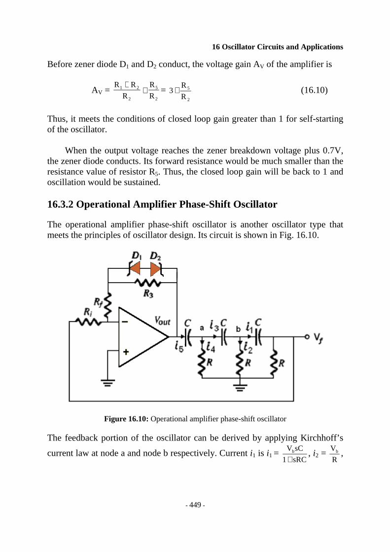
Figure 16.10: Operational amplifier phase-shift oscillator
The feedback portion of the oscillator can be derived by applying Kirchhoff’s
current law at node a and node b respectively. Current i1 is i1 = sRC1
sCVb
+, i2 =
R
Vb ,
16 Oscillator Circuits and Applications
- 450 -
i3 = (Va – Vb)sC, i4 = R
Va , and i5 = (Vout – Va)sC. Voltage at node b is also equal
to Vb = fVsRC
sRC1 ⋅+ .
At node b, current i3 = i1 + i2; R
V
sRC1
sCVsC)VV( bb
ba ++
=− . This implies that
Va =
+++
1sRc
1
sRC1
1Vb .
At node a, i5 = i1 +i2 +i4; R
V
R
V
sRC1
sCVsC)VV( abb
aout +++
=− . This implies that
sCVR
V
R
V
sRC1
sCVsCV a
abbout +++
+= . Substituting the expression of Va and Vb into
the above equation yields equation (16.10), which is the feedback portion β.
β = V
Vout
f = 1RC5CR6CR
CR22223333
3333
+ω+ω+ωω
jjj
j (16.11)
After applying Barkhausen principle of oscillator design, from real part of the complex number denominator, which is (1-6ω2R2C2) = 0, the resonant frequency fr of the oscillator shall be
fr = 1
2 6π RC (16.12)
From the imaginary part of the complex number, which is 1RC5CR
ACR3333
V3333
=ω+ω
ωjj
j,
the voltage gain AV of the amplifier shall be
AV = 15
2 2 2−ω R C
(16.13)
From equation (16.12), this shall mean that ω22 2
1
6=
R C. Substituting this
expression into equation (16.13), it yields AV = -29. This shall mean that the attenuation of the three-section RC feedback is 29. Therefore, the value of |Rf/Ri| should be 29.
16 Oscillator Circuits and Applications
- 451 -
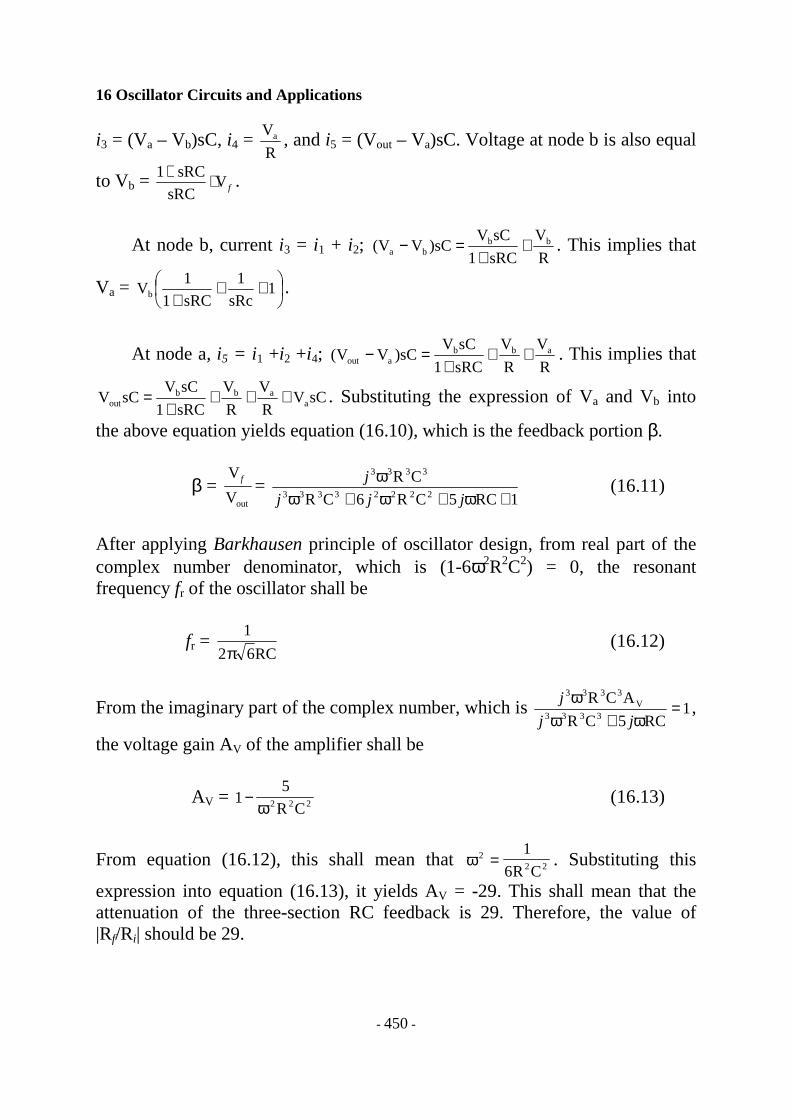
16.3.3 Quadrature Oscillator Quadrature oscillator as shown Fig. 16.11 generates two signals both sine and cosine that are in quadrature meaning out of phase by 900. The sine and cosine outputs can be arbitrary assigned. It is not necessary to assign output of operational amplifier 1 as sine output and output of operational amplifier 2 as cosine output.
The feedback portion β is Vin1/VO2 = sRC1
1
+. The gain of operational
amplifier 1 is AVO1 = sRC
sRC1+ . Similarly, the gain of operational amplifier 2 is
AVO2 = sRC
1− . The overall gain AV is ( )2sRC
sRC1+− . Applying Barkhausen principle
of oscillator design, the loop-gain of the oscillator is AVβ =sRC1
1
+−
( )2sRC
sRC1+⋅ =
( )2sRC
1− and is equal to one. This shall imply that s2R2C2 = -1. Based on this
equation, frequency f of the oscillator is
RC2
1
π=f (16.14)
Figure 16.11: Quadrature oscillator
16 Oscillator Circuits and Applications
- 452 -
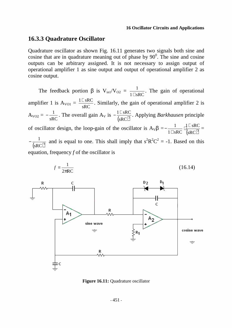
Substituting equation (16.14) into the equation of feedback portion β, which is
V in1/Vo2 = sRC1
1
+, the feedback portion β is
j+1
1 = 0452
1 −∠ . This shall mean
that its magnitude is 2
1 . This implies that overall open loop gain of the
oscillator AV is 41.12 = . The gain function is AVo1 = sRC
sRC1+ , after substituting
ω with equation (16.14), the gain function becomes AVO1 = )1( jj +− = 0452 −∠ . Similarly the gain function AVo2 is AVo2 =
sRC
1− = 0901∠ . The total
phase shift is -450 - 450 + 900 = 0 that meets the design principle.
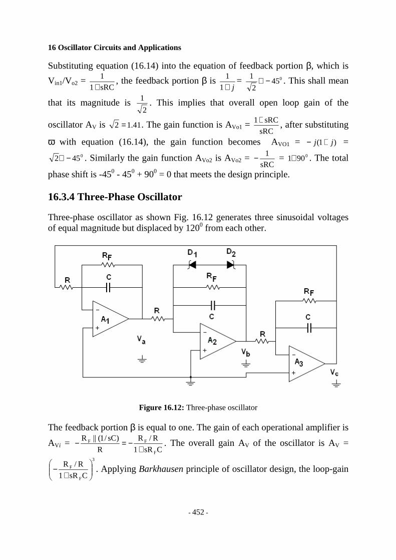
16.3.4 Three-Phase Oscillator Three-phase oscillator as shown Fig. 16.12 generates three sinusoidal voltages of equal magnitude but displaced by 1200 from each other.
Figure 16.12: Three-phase oscillator The feedback portion β is equal to one. The gain of each operational amplifier is
AVi = CsR1
R/R
R
)sC/1(||R
F
FF
+−=− . The overall gain AV of the oscillator is AV =
3
F
F
CsR1
R/R
+− . Applying Barkhausen principle of oscillator design, the loop-gain
16 Oscillator Circuits and Applications
- 453 -
of the oscillator shall be AVβ =3
F
F
CsR1
R/R
+− = 1. This implies that
0R
R1)CsR(3)CsR(3)CsR(
3
FF
2F
3F =
++++ . Equating the imaginary part of the
equation, it gives rise to the frequency of the oscillator to be
CR2
3
Fπ=f (16.15)
Equating the real part of the equation, it gives rise to the gain of individual
integrator to be 2R
RF = . Substituting the gain equation and frequency equation
into AVi = CsR1
R/R
F
F
+− , it produces gain function
31
2
j+− = 01201∠ .
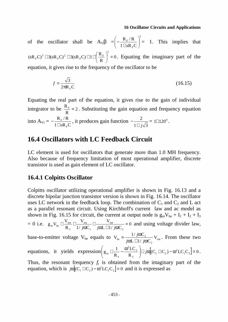
16.4 Oscillators with LC Feedback Circuit LC element is used for oscillators that generate more than 1.0 MH frequency. Also because of frequency limitation of most operational amplifier, discrete transistor is used as gain element of LC oscillator. 16.4.1 Colpitts Oscillator Colpitts oscillator utilizing operational amplifier is shown in Fig. 16.13 and a discrete bipolar junction transistor version is shown in Fig. 16.14. The oscillator uses LC network in the feedback loop. The combination of C1 and C2 and L act as a parallel resonant circuit. Using Kirchhoff's current law and ac model as shown in Fig. 16.15 for circuit, the current at output node is gmVbe + I1 + I2 + I3
= 0 i.e. 0C/1L
V
C/1
V
R
VVg
2
out
1
out
3
outbem =
ω+ω+
ω++
jjj and using voltage divider law,
base-to-emitter voltage Vbe equals to out2
2be V
C/1L
C/1V
ω+ωω
=jj
j. From these two
equations, it yields expression [ ] 0CLC)CC(R
LC
R
1g 21
221
3
22
3m =ω−+ω+
ω−+ j .
Thus, the resonant frequency fr is obtained from the imaginary part of the equation, which is [ ] 0CLC)CC( 21
221 =ω−+ωj and it is expressed as
16 Oscillator Circuits and Applications
- 454 -
fr =
21
21
CC
CCL2
1
+π
(16.16)
Figure 16.13: Colpitts oscillator
From the real part of equation [ ] 0CLC)CC(R
LC
R
1g 21
221
3
22
3m =ω−+ω+
ω−+ j , it
yields 3
m3
22
R
1g
R
LC+=
ω. Combining this equation with equation (16.16), it
yields gain AV = gmR3 = C2/C1. Thus, the feedback portion shall be β = C1/C2.
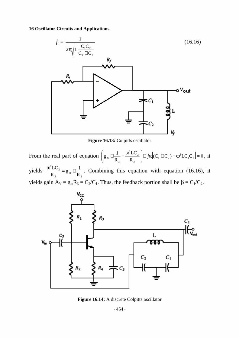
Figure 16.14: A discrete Colpitts oscillator
16 Oscillator Circuits and Applications
- 455 -
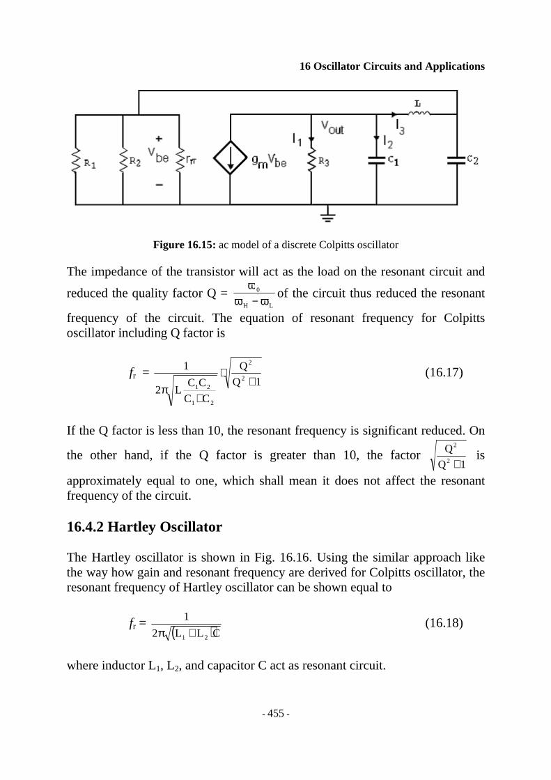
Figure 16.15: ac model of a discrete Colpitts oscillator The impedance of the transistor will act as the load on the resonant circuit and
reduced the quality factor Q = ω
ω ω0
H L−of the circuit thus reduced the resonant
frequency of the circuit. The equation of resonant frequency for Colpitts oscillator including Q factor is
fr = 1Q
Q
CC
CCL2
12
2
21
21+
⋅
+π
(16.17)
If the Q factor is less than 10, the resonant frequency is significant reduced. On
the other hand, if the Q factor is greater than 10, the factor 1Q
Q2
2
+ is
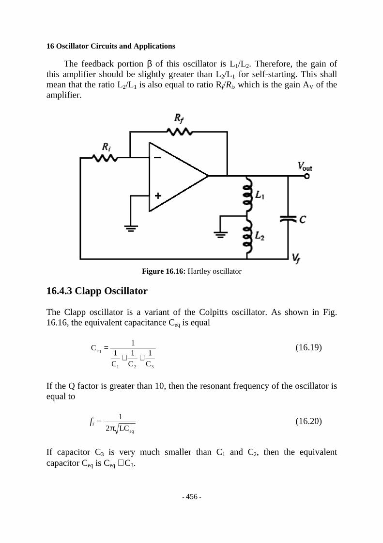
approximately equal to one, which shall mean it does not affect the resonant frequency of the circuit. 16.4.2 Hartley Oscillator The Hartley oscillator is shown in Fig. 16.16. Using the similar approach like the way how gain and resonant frequency are derived for Colpitts oscillator, the resonant frequency of Hartley oscillator can be shown equal to
fr = ( )CLL2
1
21 +π (16.18)
where inductor L1, L2, and capacitor C act as resonant circuit.
16 Oscillator Circuits and Applications
- 456 -
The feedback portion β of this oscillator is L1/L2. Therefore, the gain of this amplifier should be slightly greater than L2/L1 for self-starting. This shall mean that the ratio L2/L1 is also equal to ratio Rf/Ri, which is the gain AV of the amplifier.
Figure 16.16: Hartley oscillator
16.4.3 Clapp Oscillator The Clapp oscillator is a variant of the Colpitts oscillator. As shown in Fig. 16.16, the equivalent capacitance Ceq is equal
321
eq
C
1
C
1
C
11
C++
= (16.19)
If the Q factor is greater than 10, then the resonant frequency of the oscillator is equal to
fr = eqLC2
1
π (16.20)
If capacitor C3 is very much smaller than C1 and C2, then the equivalent capacitor Ceq is Ceq ≅ C3.
16 Oscillator Circuits and Applications
- 457 -
Figure 16.17: Clapping oscillator
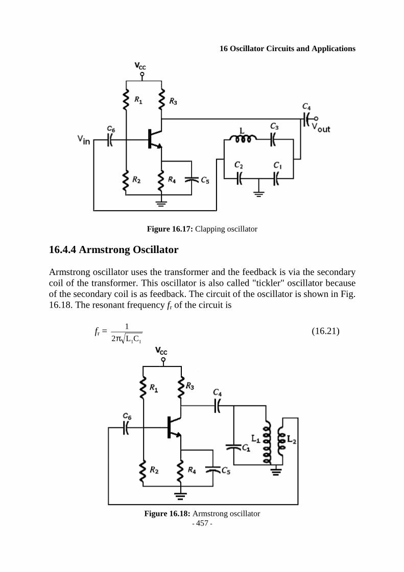
16.4.4 Armstrong Oscillator Armstrong oscillator uses the transformer and the feedback is via the secondary coil of the transformer. This oscillator is also called "tickler" oscillator because of the secondary coil is as feedback. The circuit of the oscillator is shown in Fig. 16.18. The resonant frequency fr of the circuit is
fr = 11CL2
1
π (16.21)
Figure 16.18: Armstrong oscillator
16 Oscillator Circuits and Applications
- 458 -
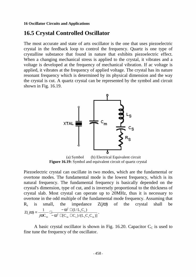
16.5 Crystal Controlled Oscillator The most accurate and state of arts oscillator is the one that uses piezoelectric crystal in the feedback loop to control the frequency. Quartz is one type of crystalline substance that found in nature that exhibits piezoelectric effect. When a changing mechanical stress is applied to the crystal, it vibrates and a voltage is developed at the frequency of mechanical vibration. If ac voltage is applied, it vibrates at the frequency of applied voltage. The crystal has its nature resonant frequency which is determined by its physical dimension and the way the crystal is cut. A quartz crystal can be represented by the symbol and circuit shown in Fig. 16.19.
(a) Symbol (b) Electrical Equivalent circuit
Figure 16.19: Symbol and equivalent circuit of quartz crystal Piezoelectric crystal can oscillate in two modes, which are the fundamental or overtone modes. The fundamental mode is the lowest frequency, which is its natural frequency. The fundamental frequency is basically depended on the crystal's dimension, type of cut, and is inversely proportional to the thickness of crystal slab. Most crystal can operate up to 20MHz, thus it is necessary to overtone in the odd multiple of the fundamental mode frequency. Assuming that Rs is small, the impedance Z(jω) of the crystal shall be
)]CCL/()CC[
)CL/1(
C
1)(Z
msssm2
ss2
m ++ω−+ω−
⋅ω
=ωj
j .
A basic crystal oscillator is shown in Fig. 16.20. Capacitor CC is used to
fine tune the frequency of the oscillator.
16 Oscillator Circuits and Applications
- 459 -
Figure 16.20: Crystal oscillator
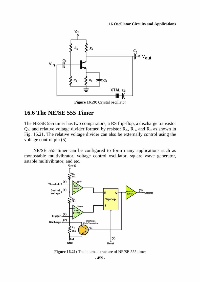
16.6 The NE/SE 555 Timer The NE/SE 555 timer has two comparators, a RS flip-flop, a discharge transistor Qd, and relative voltage divider formed by resistor RA, RB, and RC as shown in Fig. 16.21. The relative voltage divider can also be externally control using the voltage control pin (5).
NE/SE 555 timer can be configured to form many applications such as monostable multivibrator, voltage control oscillator, square wave generator, astable multivibrator, and etc.
Figure 16.21: The internal structure of NE/SE 555 timer
16 Oscillator Circuits and Applications
- 460 -
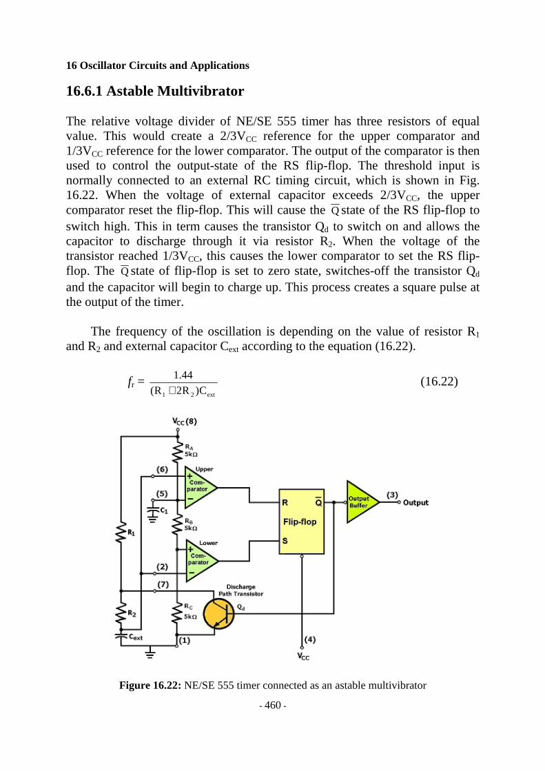
16.6.1 Astable Multivibrator The relative voltage divider of NE/SE 555 timer has three resistors of equal value. This would create a 2/3VCC reference for the upper comparator and 1/3VCC reference for the lower comparator. The output of the comparator is then used to control the output-state of the RS flip-flop. The threshold input is normally connected to an external RC timing circuit, which is shown in Fig. 16.22. When the voltage of external capacitor exceeds 2/3VCC, the upper comparator reset the flip-flop. This will cause the Qstate of the RS flip-flop to switch high. This in term causes the transistor Qd to switch on and allows the capacitor to discharge through it via resistor R2. When the voltage of the transistor reached 1/3VCC, this causes the lower comparator to set the RS flip-flop. The Qstate of flip-flop is set to zero state, switches-off the transistor Qd and the capacitor will begin to charge up. This process creates a square pulse at the output of the timer.
The frequency of the oscillation is depending on the value of resistor R1 and R2 and external capacitor Cext according to the equation (16.22).
fr = ext21 C)R2R(
44.1
+ (16.22)
Figure 16.22: NE/SE 555 timer connected as an astable multivibrator
16 Oscillator Circuits and Applications
- 461 -
The duty cycle of the pulse at output is not symmetrical because the external capacitor Cext is charged through resistor R1 and R2 and discharged through resistor R2 only. Moreover, the charging occurs from voltage 1/3VCC to 2/3VCC and the discharging occurs from voltage 2/3 VCC to 1/3VCC. The charging of external capacitor constitutes the time duration tH for the output is high and it follows equation (16.23). tH = 0.693(R1 + R2)Cext (16.23) The time tL is the time duration when the output is low. It follows equation (16.24). tL = 0.693R2Cext (16.24) The period T of the output waveform is equal to the sum of tH and tL, which is T = 0.693(R1 + 2R2)Cext (16.25) The reciprocal of period T is the frequency of the output waveform, which is also equation (16.22). The charging time tH can be obtained from charging
equation VCext = VCC + ext21 C)RR/(tCC
CC eV3
V +−
− by setting VCext = 2VCC/3, which
yields tH = (R1 + R2)Cext ln 2, whilst the discharge time can be obtained from
equation VCext = ext2CR/tCC e3
V2 − by setting VCext = VCC/3, which yields tL = R2Cext
ln 2. The duty cycle of the waveform follows equation (16.26).
Duty cycle = %100xtt
t
HL
H
+= %100x
R2R
RR
21
21
++
(16.26)
To obtain closed to 50% duty cycle, the value of resistor R2 has to be much greater than the value of resistor R1. This will make the charging and discharging times of the external capacitor Cext almost the same since R1 + R2 is approximately equal to R2. If the pulse is properly negatively offset, then a square wave is obtained.
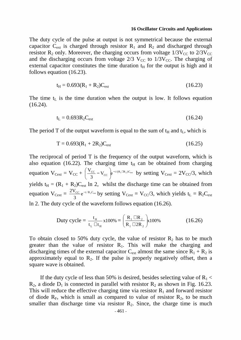
If the duty cycle of less than 50% is desired, besides selecting value of R1 < R2, a diode D1 is connected in parallel with resistor R2 as shown in Fig. 16.23. This will reduce the effective charging time via resistor R1 and forward resistor of diode RF, which is small as compared to value of resistor R2, to be much smaller than discharge time via resistor R2. Since, the charge time is much
16 Oscillator Circuits and Applications
- 462 -
shorter than discharge time, the duty cycle is less than 50%. Duty cycle is now governed by equation (16.27).
Duty cycle = %100xRRR
RR
2diode1
diode1
+++
(16.27)
Rdiode is the forward resistance of the diode, which can be assumed to be zero as compared with the value of R1 and R2.
Figure 16.23: NE/SE 555 timer configured for less than 50% duty cycle
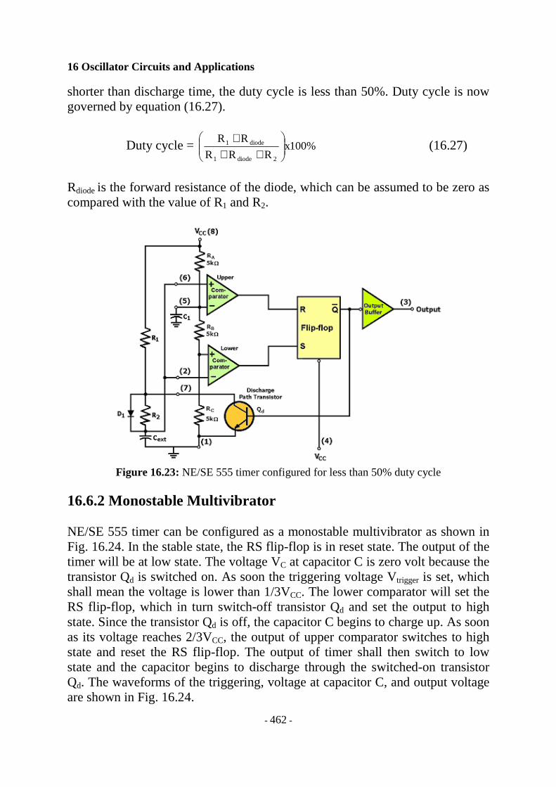
16.6.2 Monostable Multivibrator NE/SE 555 timer can be configured as a monostable multivibrator as shown in Fig. 16.24. In the stable state, the RS flip-flop is in reset state. The output of the timer will be at low state. The voltage VC at capacitor C is zero volt because the transistor Qd is switched on. As soon the triggering voltage Vtrigger is set, which shall mean the voltage is lower than 1/3VCC. The lower comparator will set the RS flip-flop, which in turn switch-off transistor Qd and set the output to high state. Since the transistor Qd is off, the capacitor C begins to charge up. As soon as its voltage reaches 2/3VCC, the output of upper comparator switches to high state and reset the RS flip-flop. The output of timer shall then switch to low state and the capacitor begins to discharge through the switched-on transistor Qd. The waveforms of the triggering, voltage at capacitor C, and output voltage are shown in Fig. 16.24.
16 Oscillator Circuits and Applications
- 463 -
Figure 16.24: NE/SE 555 timer configured as a monostable multivibrator
The pulse width twidth of the monostable multivibrator is calculated from the charging time of RC network charging for voltage from zero volt to 2/3VCC. The pulse width follows equation (16.28).
twidth = 1.098RC (16.28) Pulse width twidth can be obtained from universal charging/discharging equation VC = Vf + (Vi –Vf)exp(-t/τ), where Vi = 0 and Vf = VCC that yields equation VC = VCC – VCCexp(-twidth/RC). By setting VC = 2VCC/3, the final charge voltage of capacitor, it yields twidth = RC ln 3.
If the triggering voltage Vtrigger is a pulse of known frequency and the time twidth is controlled such that it is equal to 1.2 times of the period T of Vtrigger pulse then the monostable multivibrator is become a divide-by-two frequency divider.
In general, for the monostable multivibrator to be configured as divide-by-n frequency divider, the pulse-width twidth should be equal to [0.2 + (n-1)]T. 16.6.3 Voltage Controlled Oscillator The NE/SE 555 timer can also be configured as a voltage controlled oscillator VCO. This can be achieved by connecting an external voltage Vcont to voltage
16 Oscillator Circuits and Applications
- 464 -
control pin (5). The external voltage changes the threshold value of the lower and upper comparator from 1/3VCC to 1/2Vcont and 2/3VCC to Vcont. An increase of Vcont value increases the charging and discharging time and causes the frequency of the output waveform to decrease and vice versa. The period T of voltage controlled oscillator VCO can be obtained from the universal charging/discharging equation VCext = Vf + (Vi –Vf)exp(-t/τ).
During the charging phase, Vi = 2
Vcont and Vf = VCC, thus, the charging
equation shall be VCext = VCC + ext21 C)RR/(tCC
cont eV2
V +−
− . Setting VCext = Vcont, the
charging time tH shall be
tH = (R1 + R2)Cext
−−
contCC
contCC
VV
2/VVln (16.29)
During the discharging phase, Vi = VCont and Vf = 0, thus, the charging equation shall be VCext = ext2CR/t
conteV − . Setting VCext = Vcont/2, the discharging time tL shall be
tL = R2Cext 2ln (16.30) The period T of the VCO is
T = (R1 + R2)Cext
−−
contCC
contCC
VV
2/VVln + R2Cext 2ln (16.31)
The voltage controlled ascillator can be implemented using a integrated circuit NE/SE 566 chip. This intergated circuit VCO produces two simultaneously square wave and triangular wave at the frequency upto 1.0 MHz. The basic block diagram of the VCO is shown in Fig. 16.25.
VCO can also be considered as voltage-to-frequency converter since the input voltage determines the frequency of the output. NE/SE 566 VCO has a current source that consists of the lower current source and upper current source. The schmitt trigger has two threshold voltages namely the lower threshold voltage VL and upper threshold voltage VH. The upper current source is used to charge the external capacitor from VL voltage to VH voltage. The lower current source is used to discharge the external capacitor from VH voltage to VL voltage. Beside providing square wave, the output of the schmitt trigger is
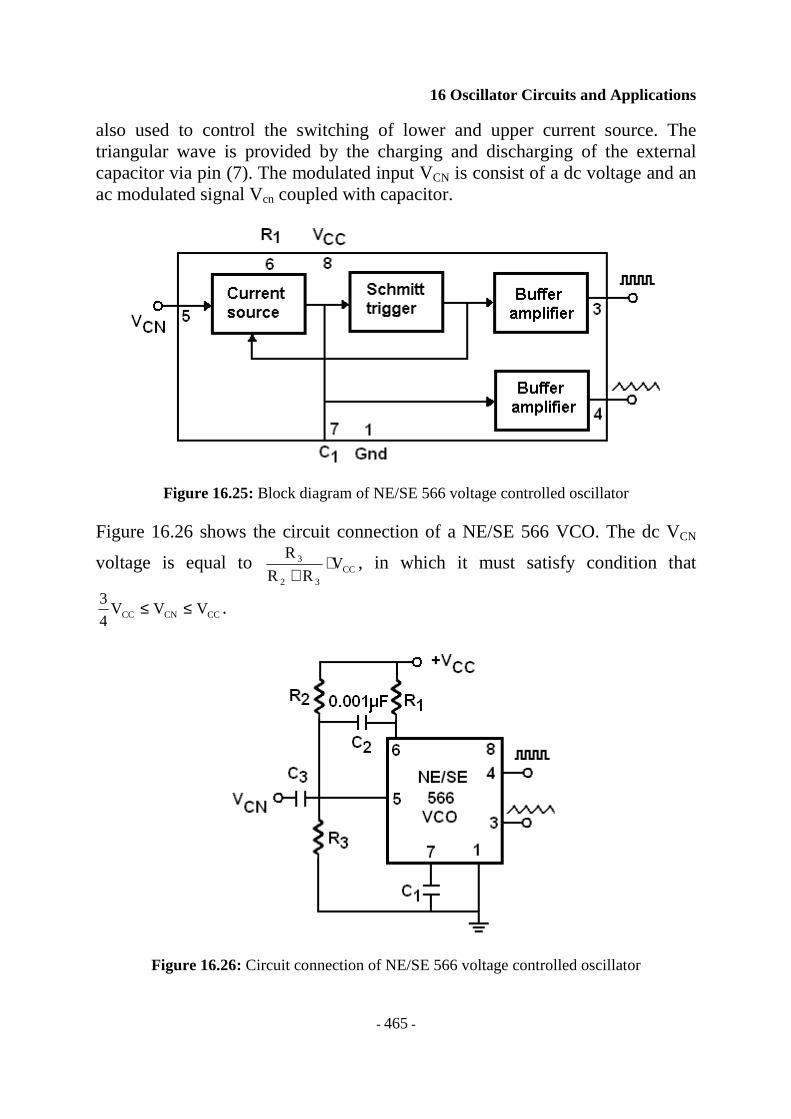
16 Oscillator Circuits and Applications
- 465 -
also used to control the switching of lower and upper current source. The triangular wave is provided by the charging and discharging of the external capacitor via pin (7). The modulated input VCN is consist of a dc voltage and an ac modulated signal Vcn coupled with capacitor.
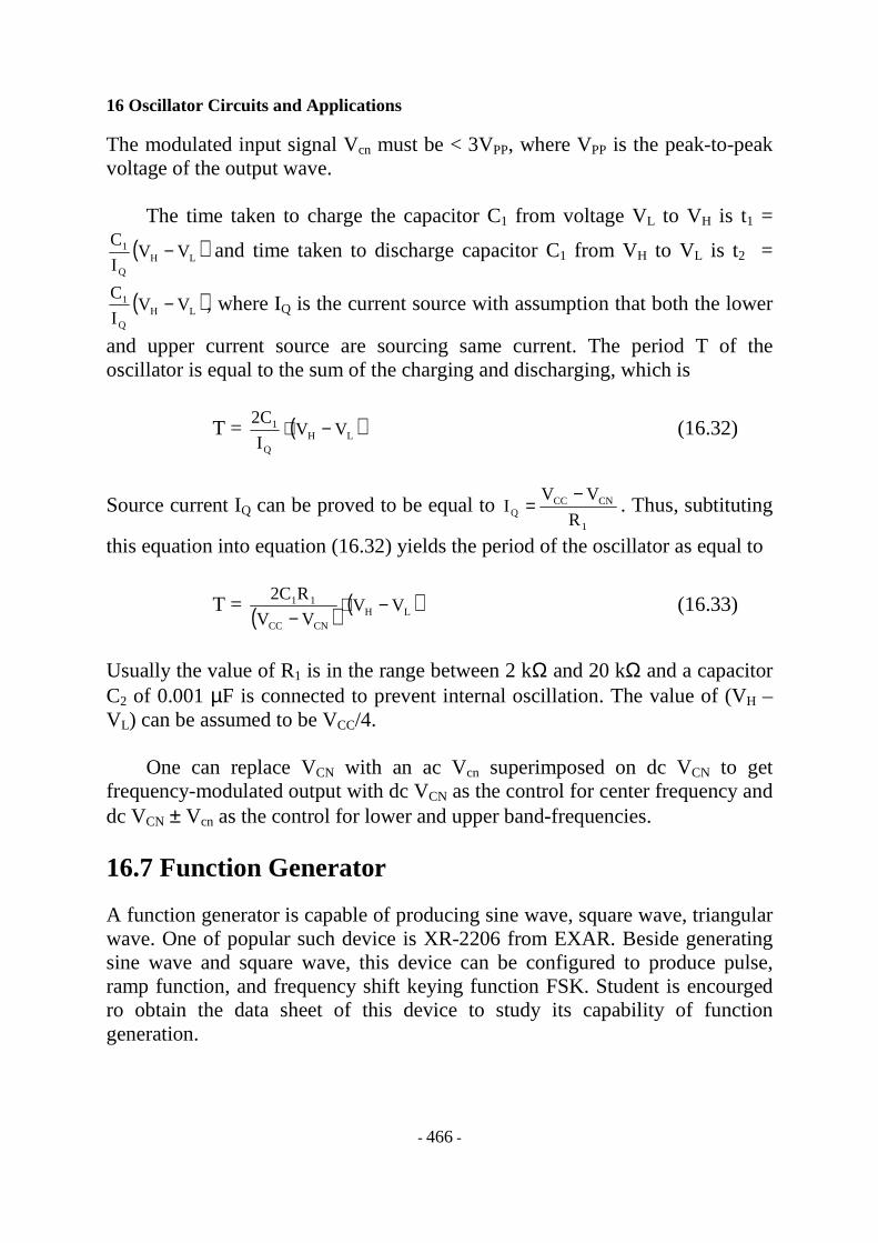
Figure 16.25: Block diagram of NE/SE 566 voltage controlled oscillator Figure 16.26 shows the circuit connection of a NE/SE 566 VCO. The dc VCN
voltage is equal to CC32
3 VRR
R⋅
+, in which it must satisfy condition that
CCCNCC VVV4
3 ≤≤ .
Figure 16.26: Circuit connection of NE/SE 566 voltage controlled oscillator
16 Oscillator Circuits and Applications
- 466 -
The modulated input signal Vcn must be < 3VPP, where VPP is the peak-to-peak voltage of the output wave.
The time taken to charge the capacitor C1 from voltage VL to VH is t1 =
( )LHQ
1 VVI
C− and time taken to discharge capacitor C1 from VH to VL is t2 =
( )LHQ
1 VVI
C− , where IQ is the current source with assumption that both the lower
and upper current source are sourcing same current. The period T of the oscillator is equal to the sum of the charging and discharging, which is
T = ( )LHQ
1 VVI
C2−⋅ (16.32)
Source current IQ can be proved to be equal to 1
CNCCQ R
VVI
−= . Thus, subtituting
this equation into equation (16.32) yields the period of the oscillator as equal to
T = ( ) ( )LHCNCC
11 VVVV
RC2−⋅
− (16.33)
Usually the value of R1 is in the range between 2 kΩ and 20 kΩ and a capacitor C2 of 0.001 µF is connected to prevent internal oscillation. The value of (VH – VL) can be assumed to be VCC/4.
One can replace VCN with an ac Vcn superimposed on dc VCN to get frequency-modulated output with dc VCN as the control for center frequency and dc VCN ± Vcn as the control for lower and upper band-frequencies.
16.7 Function Generator A function generator is capable of producing sine wave, square wave, triangular wave. One of popular such device is XR-2206 from EXAR. Beside generating sine wave and square wave, this device can be configured to produce pulse, ramp function, and frequency shift keying function FSK. Student is encourged ro obtain the data sheet of this device to study its capability of function generation.
16 Oscillator Circuits and Applications
- 467 -
16.8 Phase-Lock Loop Let’s consider a phase-lock loop, which is often using in the communication circuit as the input frequency locker. There are many other applications of the phase-lock loop PLL such as used in FM stereo decoders, tracking filter FSK decoder, and frequency-synthesized transmitters and receivers.
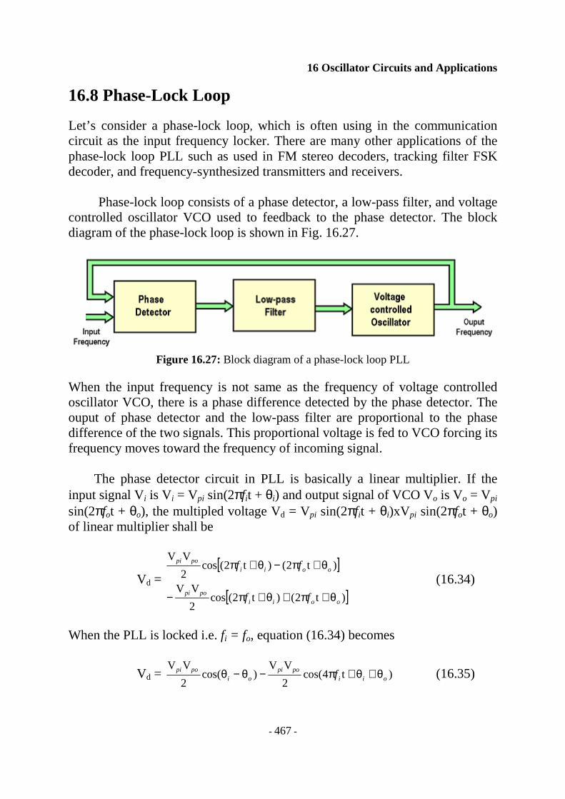
Phase-lock loop consists of a phase detector, a low-pass filter, and voltage controlled oscillator VCO used to feedback to the phase detector. The block diagram of the phase-lock loop is shown in Fig. 16.27.
Figure 16.27: Block diagram of a phase-lock loop PLL
When the input frequency is not same as the frequency of voltage controlled oscillator VCO, there is a phase difference detected by the phase detector. The ouput of phase detector and the low-pass filter are proportional to the phase difference of the two signals. This proportional voltage is fed to VCO forcing its frequency moves toward the frequency of incoming signal.
The phase detector circuit in PLL is basically a linear multiplier. If the input signal Vi is Vi = Vpi sin(2πfit + θi) and output signal of VCO Vo is Vo = Vpi sin(2πfot + θo), the multipled voltage Vd = Vpi sin(2πfit + θi)xVpi sin(2πfot + θo) of linear multiplier shall be
Vd = [ ]
[ ])t2()t2(cos2
VV
)t2()t2(cos2
VV
ooiipopi
ooiipopi
ff
ff
θ+π+θ+π−
θ+π−θ+π (16.34)
When the PLL is locked i.e. fi = fo, equation (16.34) becomes
Vd = )t4cos(2
VV)cos(
2
VVoii
popioi
popi f θ+θ+π−θ−θ (16.35)
16 Oscillator Circuits and Applications
- 468 -
The second term of equation (16.35) contains the second harmonic signal, which shall be filtered out by the low-pass filter. Thus, the control voltage VC to VCO is
VC = )cos(2
VVoi
popi θ−θ (16.36)
(θi -θo) is called phase error. Thus, the output of filter is proportional to the phase error.
The phase-lock loop has three modes of operation. When there is no input signal to the phase detector, the voltage controlled oscillator VCO is running at a fixed frequency called center frequency fo corresponds to zero input voltage that has characteristic fo(t) = fo + KoVC(t), where Ko is the sensitivity of voltage control oscillator VCO. The phase-lock loop is said to be in free running mode.
When there is input signal, the phase-lock loop goes into capture mode. The frequency of the voltage controlled oscillator changes continuously to match the input frequency. Once the input frequency is equal to the output frequency of voltage controlled oscillator, the phase-lock loop is said to be phase-lock mode.
The time taken for a phase-lock loop PLL to capture the incoming signal is called capture time or pull-in-time. This time depends on the initial frequency and phase difference (θi - θo) between Vi and Vo as well as the filter and other loop characteristics.
The most commonly used integrated circuit PLL is NE/SE 565. The center
frequency fo of the this chip is fo = 11CR4
2.1 . R1 and C1 are external resistor and
capacitor connected to pin (8) and pin (9) of the chip respectively.
The NE/SE 565 PLL typically can track and lock input frequency over bandwidth ±60% of the center frequency fo. The lock range of the chip fL is fL =
EECC
o
VV
8
−f
. The capture range of the chip is fc = 2
3L
C10x6.3x2πf
, where C2 is the
capacitor connected between VCC and modulated output pin (7). Typically the value of C2 is 10µF.
16 Oscillator Circuits and Applications
- 469 -
Exercises 16.1. State the principles for designing an oscillator and draw a block diagram
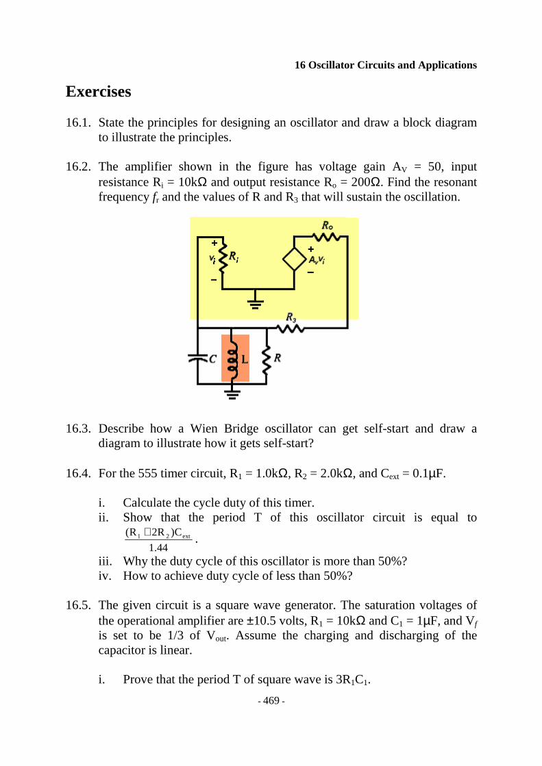
to illustrate the principles. 16.2. The amplifier shown in the figure has voltage gain AV = 50, input
resistance Ri = 10kΩ and output resistance Ro = 200Ω. Find the resonant frequency fr and the values of R and R3 that will sustain the oscillation.
16.3. Describe how a Wien Bridge oscillator can get self-start and draw a
diagram to illustrate how it gets self-start? 16.4. For the 555 timer circuit, R1 = 1.0kΩ, R2 = 2.0kΩ, and Cext = 0.1µF.
i. Calculate the cycle duty of this timer. ii. Show that the period T of this oscillator circuit is equal to
44.1
C)R2R( ext21 + .
iii. Why the duty cycle of this oscillator is more than 50%? iv. How to achieve duty cycle of less than 50%?
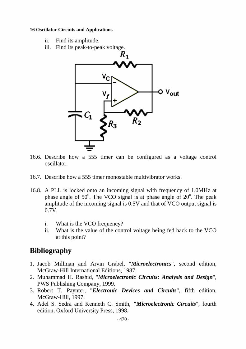
16.5. The given circuit is a square wave generator. The saturation voltages of
the operational amplifier are ±10.5 volts, R1 = 10kΩ and C1 = 1µF, and Vf is set to be 1/3 of Vout. Assume the charging and discharging of the capacitor is linear.
i. Prove that the period T of square wave is 3R1C1.
16 Oscillator Circuits and Applications
- 470 -
ii. Find its amplitude. iii. Find its peak-to-peak voltage.
16.6. Describe how a 555 timer can be configured as a voltage control
oscillator. 16.7. Describe how a 555 timer monostable multivibrator works. 16.8. A PLL is locked onto an incoming signal with frequency of 1.0MHz at
phase angle of 500. The VCO signal is at phase angle of 200. The peak amplitude of the incoming signal is 0.5V and that of VCO output signal is 0.7V.
i. What is the VCO frequency? ii. What is the value of the control voltage being fed back to the VCO
at this point?
Bibliography 1. Jacob Millman and Arvin Grabel, "Microelectronics", second edition,
McGraw-Hill International Editions, 1987. 2. Muhammad H. Rashid, "Microelectronic Circuits: Analysis and Design",
PWS Publishing Company, 1999. 3. Robert T. Paynter, "Electronic Devices and Circuits", fifth edition,
McGraw-Hill, 1997. 4. Adel S. Sedra and Kenneth C. Smith, "Microelectronic Circuits", fourth
edition, Oxford University Press, 1998.


