
Chapter 9
Radio frequency scanning probe measurements of materials
9.1. Electromagnetic characterization of materials: fundamental concepts
Preceding chapters have described the near field scanning microwave microscope (NSMM), while
discussing both the underlying theory of operation and practical considerations for instrumentation. A
primary application area for NSMMs and related microscopes is broadband, local metrology of materials
with nanometer-scale spatial resolution. Several methods for spatially-resolved characterization of
materials are reviewed in this chapter. We begin by reviewing the fundamental concepts of
electromagnetic materials metrology. Furthermore, since the extraction of quantitative information from
NSMM measurements requires appropriate modeling of the measurement system, we will describe
strategies for modeling probe-material interactions. Once the fundamental concepts and models have
been established, we will review several applications of scanning-probe-based metrology to local
characterization of electromagnetic materials.
Just as Maxwell’s equations are fundamental to the characterization of electromagnetic devices, they are
also fundamental to electromagnetic characterization of materials. In Chapter 2, we introduced the
Maxwell-Lorentz microscopic equations. To proceed from the microscopic equations to a description of
electromagnetic fields in materials, it is reasonable to start with the introduction of the constitutive
relations for polarization and magnetization. In addition to the time-dependent charge and current
distributions, the Maxwell-Lorentz equations also require specification of the relationship between the
polarization P, magnetization M, and the electromagnetic fields E and B, as well as their space and time
derivatives. These relations are called constitutive relations. Note that the magnetization and polarization
may each depend on both the electric and magnetic fields. While these concepts are especially useful for
emerging materials like ferromagnetic-ferroelectric composites, photonic bandgap crystals, or
metamaterials, each class of materials may require a customized approach. Therefore, it is important to
have a fundamental understanding of the constitutive relations in Maxwell’s equations. In general, the
primary objective is to describe the general electromagnetic response of a material, starting from the
microscopic quantities and subsequently averaging to get the macroscopic quantities. This chapter is
primarily concerned with the local, spatially-resolved measurement techniques of spatially varying
quantities at small length scales. Techniques for macroscopic microwave measurements of dielectric
properties and techniques for electromagnetic characterization of bulk materials are addressed in
numerous texts [1]-[4].
The constitutive relations can be expressed in the form
𝑷 ⟺ {𝑬, 𝑩}, 𝑴 ⟺{B, E} , (9.1)
where ⟺ indicates that this relationship can be either local or nonlocal in both time and space. Further,
these relations can be either linear or nonlinear functions of the driving fields [1]. Note that the dielectric
polarization is odd under parity transformation and even under time reversal while the magnetization is
even under parity transformation and odd under time reversal. Although E and B are widely accepted as
fundamental fields, here we will use E and H as driving fields that may be time dependent.
The introduction of constitutive relations for polarization and magnetization gives rise to complications
due to the fact that they depend not only on the applied fields but also on the internal energy of the
investigated material in its given state. In the case of magnetization, the response originates from moving
charge and spin, as described by Bloch or Landau-Lifshitz equations [3]. These phenomenological
equations relate the time-dependent magnetization to both the external magnetic field and the internal
energy. The behavior of dielectric materials originates from charge as well electric multipole moments.
The description of the time-dependent polarization response is more complex because the motion of
charges and multipoles induces magnetic fields in the material in addition to electric fields. Furthermore,
under ambient conditions only a small percentage of electric dipoles are fully aligned with an applied
electric field due to thermal effects. Naturally, the situation becomes even more complicated in composite
materials. For example, in magneto-electric materials, complex coupling mechanisms include the electric-
field-induced shift of the Landé g factor, spin-orbit interactions, exchange energies and the electric-field-
induced shift of single ion anisotropy energies [5], [6]. The general approach presented here follows
References [7] and [8] and includes the possibility of magneto-electric coupling within the material, but
the results can be extended to materials without such coupling. For micro- or nanoscale materials, the
microscopic approach is necessary, however some problems in RF nanoelectronics can be treated by
averaging the microscopic quantities to find macroscopic quantities that can be used instead.
The standard materials relations in Maxwell’s equations are often expressed in terms of the effective
macroscopic polarization and magnetization. The magnetic induction is related to the magnetic field H
and the magnetization M by
𝑩 = 𝜇0(𝑯 + 𝑴) , (9.2)
while the electric displacement is related to the electric field polarization and the macroscopic
quadrupole density �̃� by
𝑫 = 휀0𝑬 + �̃� − 𝛁 ∙ [�̃�] = 휀0𝑬 + 𝑷 . (9.3)
�̃� is the macroscopic dipole density, while 0 and 0 are the permittivity and permeability of free space,
respectively. In order to move from the macroscopic variables to the microscopic variables, we define the
macroscopic variables in terms of microscopic densities. The microscopic dipole density with the
quadrupole-moment distribution for N particles is
𝒑 = ∑ 𝒓𝑗𝑒𝑗𝛿(𝒓 − 𝒓𝑗)𝑁𝑗=1 −
1
2∑ 𝑒𝑗(𝒓𝑗𝒓𝑗)∇𝑁
𝑗=1 𝛿(𝒓 − 𝒓𝑗) = ∑ 𝐩𝑗𝑗 . (9.4)
The index j = 1, 2…N. The position of the j-th particle is rj. The charge on the j-th particle ej can be positive
or negative. The summation is over the bound charge, which is electrically neutral as a whole. The same
condition also applies to the free charge. The motion of the free charge gives rise to kinetic energy that
has to be included in the internal energy of the system. Similarly, the microscopic magnetic dipole density
is

𝒎 = ∑ {𝛾𝑖𝒔𝑖(𝒓𝑖)𝛿(𝒓 − 𝒓𝑖) −𝛾𝑒𝑖
𝑒𝑖𝝅𝑖 × 𝐩𝑖}𝑖 ≡ ∑ 𝒎𝑖 + 𝒎𝑂𝑖 . (9.5)
Equation (9.5) clearly separates the magnetic dipole density into contributions from spin and from
charge motion.
The gyromagnetic ratio is
𝛾𝑖 = 𝑔𝑖𝜇0𝑒𝑖 2𝑚𝑠𝑖⁄ , (9.6)
where msi is the mass of the electron, gi is the spectroscopic Landé factor and s is the intrinsic spin. In
addition,
𝛾𝑒𝑖 = 𝜇0𝑒𝑖 2𝑚𝑠𝑖⁄ (9.7)
and the canonical momentum is given by
𝝅𝑖 = 𝑚𝑠𝑖𝒅𝒓𝒊
𝒅𝒕+ 𝑒𝑖𝑨𝑖 , (9.8)
where Ai is the vector potential. The expected values of macroscopic polarization and magnetization are
found by averaging:
𝑷(𝒓, 𝑡) =< 𝐩 >= 𝑇𝑟[𝐩𝜌(𝑡)] (9.9a)
𝑴(𝒓, 𝑡) =< 𝒎 >= 𝑇𝑟[𝒎𝜌(𝑡)] = ∑ < 𝒎𝑖 > (𝒓, 𝑡) +< 𝒎𝑂𝑖 > (𝒓, 𝑡) , (9.9b)
where 𝜌(𝑡) is the statistical density operator satisfying Liouville’s equations and Tr(.) is the trace operator.
Note that both 𝒑 and 𝒎 implicitly depend on functions of electric and magnetic field. By use of statistical
mechanics, it is possible to derive the evolution equations for equilibrium and non-equilibrium conditions
and the corresponding equations of motion for the magnetization and polarization, including the cross-
coupling terms. Such a comprehensive derivation is beyond the scope of this chapter, but leads to the
classical Landau-Lifshitz equation of motion for magnetization and the equation of motion for
polarization. For the interested reader, the details of the derivation can be found in Reference [7].
More complex interactions such as magneto-electric interactions may be incorporated into the equations
of motion by including all possible relationships between the polarization and magnetization with the
magnetic and electric fields. The macroscopic averages of the microscopic variables that are useful for
measurement applications are [8]
𝑷 ≈ 𝛼𝑒𝑒𝑬𝒑 + 𝛼𝑒𝑚𝑯𝒎 + 𝝌𝒆𝒔 ∙ [𝚺𝜺] + 𝝌𝒆𝒖(𝑇 − 𝑇0) , (9.10a)
𝑴 ≈ 𝛼𝑚𝑒𝑬𝒑 + 𝛼𝑚𝑚𝑯𝒎 + 𝝌𝒎𝒔 ∙ [𝚺𝜺] + 𝝌𝒎𝒖(𝑇 − 𝑇0) , (9.10b)
with
𝑬𝒑(𝒓, 𝑡) ≈ [𝝌𝒆𝒆]−𝟏 ∙ 𝑷(𝒓, 𝑡) + [𝑵𝒑] ∙ 𝑷(𝒓, 𝑡) , (9.11a)
𝑯𝒎(𝒓, 𝑡) ≈ [𝝌𝒎𝒎]−𝟏 ∙ 𝑴(𝒓, 𝑡) + [𝑵𝒎] ∙ 𝑴(𝒓, 𝑡) . (9.11b)
The tensors [𝝌𝒊𝒊] are the electric and magnetic susceptibility tensors while the tensors [𝑵𝒊] are
depolarization and demagnetization tensors. The coefficients 𝛼𝒊𝒋 are the corresponding magneto-electric
coupling coefficients. The tensor [𝚺𝜺] represents the influence of strain. Finally, within a material the
macroscopic fields differ from applied fields due to induced surface depolarization charges. For example,
the total electric field can be expressed as
𝑬𝒑(𝒓, 𝒕) = 𝑬𝟎(𝒓, 𝒕) − [𝑵𝒑] ∙ 𝑷(𝒓, 𝒕), (9.12)
where E0 is the applied field.
This brief introduction of the microscopic electromagnetic field variables provides a foundation for
describing complex materials at sub-micrometer length scales. The application of this analysis to specific
cases can be quite challenging, requiring detailed knowledge of the relevant geometrical configurations
and boundary conditions. The definitions of the electromagnetic field variables for microscopic
characterization of materials that we have introduced here provide but a starting point for extending the
theory to each particular case. Some insightful examples are described in Reference [3].
9.2. Impedance circuit models of probe-sample interactions
9.2.1 Toward materials characterization with near-field scanning microwave microscopy
We now focus on models that enable quantitative characterization of device and material properties by
use of an NSMM. In Chapter 8, we discussed the interaction of the tip with the measured sample under
test (SUT) or device under test (DUT) when the NSMM probe tip was at a certain distance above the
surface. We introduced the coupling capacitance and approaches to extract quantitative, calibrated data
from the measurements. Here, we extend the models to incorporate material properties. Materials
measurements performed by use of an NSMM usually come in one of two forms: height-dependent
measurements with the lateral position of the tip fixed or spatially-resolved NSMM images. For the latter
case, we will focus primarily on images obtained in “contact mode,” i.e. with the probe in direct
mechanical and electrical contact with the SUT.
Recall that for NSMMs that are configured as a one-port system, the measured parameter is the reflection
coefficient. The transmission coefficient is an additional measured parameter for two-port NSMM
systems. Also recall that in a NSMM, the tip–sample interaction is in the near field. In most cases the
wavelength of the applied field is much larger than the interaction dimensions and the sample dimensions
are large with respect to the tip dimensions. Thus, the modeling of the probe’s interaction with a material
or device is often done using lumped-element impedance circuits. If it is necessary to consider
propagation between two ports in a measurement system, then a transmission line model, or a hybrid
combination of lumped element and transmission line models, is likely to prove useful. If the tip and the
sample dimensions are comparable, full electromagnetic field calculations must be implemented.
Returning to the case of lumped-element impedance modeling, once the impedance is known from the

measurement, it is possible to use physical models to extract the quantitative parameters of the SUT or
DUT. Where possible, we present models generalizable to any experimental case readers may encounter.
Below we will demonstrate application of these models to some specific cases for different material
parameter categories and show how the parameters of interest can be extracted from the measurements.
9.2.2 Near-field, lumped element models
One modeling approach is to represent the tip-sample interaction by a complex, lumped element
impedance ZS. In the near- or evanescent-field regime, if the tip-sample interaction is lossless, then no net
power is transmitted into the sample. The stored reactive energy of the tip-sample interaction may be
represented by a reactance XS in the lumped element impedance. On the other hand, if the sample or tip
is lossy, energy is dissipated. Then the lumped element impedance must include a resistive part, RS. The
combined lumped element impedance is
𝑍𝑠 = 𝑅𝑠 + 𝑗𝑋𝑠 , (9.13)
where j is the imaginary unit (As discussed in Chapter 8, Zs is in series with the coupling capacitance). ZS
depends on the tip geometry, the sample properties, and the tip-sample distance. Fig. 9.1 shows an
elementary, lumped element circuit representing the tip coupled to the sample: CCpl is the coupling
capacitance, CStr is the stray or parasitic capacitance and Rtip is the probe resistance. Having previously
discussed the coupling and the stray capacitance in Chapter 8, here we turn to models of the sample
impedance. Several reasonable and practically useful models of the sample impedance were introduced
for bulk materials in Reference [9]. XS and RS can be obtained from the integration of the Poynting vector
over the whole sample volume. They can be expressed as [9],[10]:
𝑋𝑠 =4𝜔
|𝐼|2 ∫(𝑤𝑚 − 𝑤𝑒)𝑑𝑉 (9.14)
and
𝑅𝑠 =𝜔
𝐼2 ∫ (𝜎
𝜔|𝑬|2 + 휀0휀 ,,|𝑬|2 + 𝜇0𝜇 ,,|𝑯|2) 𝑑𝑉 , (9.15)
where I is the amplitude of the input current at the tip terminal. The scalar permittivity 휀𝑠 = 휀0(휀′ − 𝑗휀′′)
and the permeability 𝜇 = 𝜇0(𝜇′ − 𝑗𝜇′′). The variables 𝑤𝑚 =𝑩𝑯∗
4 and 𝑤𝑒=
𝑬𝑫∗
4 in Equation (9.14) are
magnetic and electric field densities (The asterisk represents complex conjugation of the variable). The
three terms in the integrand of Equation (9.15) represent the conductive, magnetic and dielectric losses
in the investigated material, respectively.
Figure 9.1. General circuit models of tip-sample system. (a) Lumped element circuit model of probe tip
coupled to sample. (b) Lumped element circuit model for a magnetic loop probe coupled to sample.
Adapted from S.-C Lee, C. P. Vlahacos, B. J. Feenstra, A. Schwartz, D. E. Steinhauer, F. C. Wellstood, and
S. M. Anlage, Appl. Phys. Lett. 77 (2000) pp. 4404-4406, with permission from AIP Publishing.
Examination of the total circuit impedance in Fig. 9.1(a) leads to the conclusion that maximum sensitivity
to Zs can be achieved when the coupling impedance is small with respect to Zs and the parasitic impedance

is negligible. This can usually be achieved by making the distance between the tip and the sample much
smaller than the diameter of the probe tip (e.g. when the tip is in contact with the sample). A more
rigorous statement of the near-field condition is:
|𝑘|𝑑𝑡𝑖𝑝 ≪ 1; 𝑘 = 𝜔(휀0휀𝑠𝜇0𝜇𝑠)1/2 , (9.16)
where 𝑑𝑡𝑖𝑝 is the effective tip diameter that defines the tip-sample interaction area and is the radial
operation frequency of the microscope. Thus, in the near field [9]
𝑍𝑠 ≈1
𝑗𝜔 0 𝑠𝑑𝑡𝑖𝑝 (9.17)
and the lumped element model for a lossy bulk material becomes:
𝑍𝑠 =𝑡𝑎𝑛𝛿
𝜔 0′𝑑𝑡𝑖𝑝
− 𝑗1
𝜔 0′𝑑𝑡𝑖𝑝
. (9.18)
Equation (9.18) can be modified for different classes of materials.
For example, in a low loss dielectric material with loss tangent 𝑡𝑎𝑛𝛿 ≪ 1, Equation (9.18) can be further
simplified by neglecting the first term. For a normal metal, Equation (9.18) simplifies to
𝑍𝑠 =1
𝑑𝑡𝑖𝑝𝜎 , (9.19)
which is simply the DC resistance of the interaction volume. For bulk semiconductors free of native oxides,
RS and XS are of the same order and the sample impedance can be expressed as
𝑍𝑠 =1
𝑑𝑡𝑖𝑝𝜎+𝑗𝜔 0′𝑑𝑡𝑖𝑝
, (9.20)
where 𝜎 is the conductivity of the semiconductor. Alternatively, the dielectric properties of
semiconductors and other materials can be represented by a plasma-like Lorentz-Drude permittivity [4]
휀𝑝 = 휀′ −𝜔𝑝
2
𝜔(𝜔+𝑗𝜈) , (9.21)
where 𝜔𝑝2 =
𝑒2𝑁𝜈
0𝑚𝑒𝑓𝑓 is the plasma frequency, 𝜈 is the collision frequency, e is the charge, 𝑚𝑒𝑓𝑓the
effective mass of the carrier and N is the concentration. Note that in these expressions, a harmonic
exp(jt) time dependence is assumed. The impedance is then obtained by inserting this permittivity into
Equation (9.17) in place of S.
Inductive loop probes provide an effective approach for imaging magnetic materials, albeit with poorer
resolution than sharp tip probes. A circuit model of a loop probe is illustrated in Fig. 9.1(b). In this case,
the tip sample-impedance can be expressed as [11]
𝑍𝑠 =𝜔2𝑀2
𝐺𝑍𝑠𝑢𝑟𝑓+𝑗𝜔𝐿1 , (9.22)

where G is the geometric factor, 𝑍𝑠𝑢𝑟𝑓 the complex surface impedance, M is the mutual tip sample
inductance and L1 is the effective inductance of the sample.
For a scanning-tunneling-microscope-based, resonant NSMM, a hybrid approach that combines lumped
elements and transmission lines is used. Specifically, a transmission line is used to model the transmission
resonator while a lumped element model is used to characterize the tip-sample interaction [12]. The
influence of the sample is modeled as a parallel combination of the tunneling impedance 𝑍𝑡 and the probe
impedance 𝑍𝑝
𝑍𝑆 = (𝑍𝑡 𝑍𝑝 ) (𝑍𝑡 + 𝑍𝑝)⁄ . (9.23)
Recall that in a scanning tunneling microscope, an electrically biased tip is positioned about 1 nm from a
conducting sample, giving rise to a tunneling current and corresponding tunneling impedance. If the
tunneling impedance is mostly due to dissipative losses in the tunnel junction, this impedance is effectively
just a tunneling resistance and 𝑍𝑡 ≈ 𝑅𝑒(𝑍𝑡) = 𝑅𝑡. In a typical tunneling microscope, in which the tip
height h is on the order of a nanometer, the tunneling resistance can be approximated by
𝑅𝑡(ℎ) = 𝑅0(1 + (ℎ ℎ0⁄ )𝛼) . (9.24)
The constants 𝑅0, h0 and 𝛼 are best obtained from a comparison with measurements. When the probe is
raised outside of the tunneling range, 𝑅𝑡 → ∞ and does not contribute. There can be a significant
difference in values of R0 for AC and DC operation. In the cases when the simple resistance approximation
is not valid, the tunneling impedance can be expressed as 𝑍𝑡 = 𝑅𝑡(1 + 𝑗𝜔𝜏). The tunneling impedance
should have an inductive character and therefore a corresponding characteristic time constant τ
proportional to 𝐿𝑡/𝑅𝑡 , where Lt is the tip inductance.
9.2.3 Transmission line models
In some cases, a transmission line model provides a more suitable approach to calculation of ZS. Multilayer
thin film samples, in which the incident signal may penetrate into subsurface layers, are particularly
amenable to this approach. The multilayer material is modeled as a series of cascaded transmission line
segments with each segment representing a layer of the material. For example, a transmission line can be
used to calculate ZS for the specific case of a multilayered solar cell [13], as illustrated in Fig. 9.2. The
complex impedance of the multilayer solar cell can be expressed as
𝑍𝑆 ≈ 𝑍𝑛𝑍𝑠𝑢𝑏+𝑗𝑍𝑛𝛾𝑛𝑡𝑛
𝑍𝑛+𝑗𝑍𝑠𝑢𝑏𝛾𝑛𝑡𝑛 , (9.25)
where 𝑍𝑛, 𝛾𝑛, and 𝑡𝑛 are the impedance, electromagnetic wave propagation constant and thickness of
the n-type silicon layer of the stack, respectively. If the impedances of the deepest two layers in Fig. 9.2(a)
and 9.2(b) are combined into a single parameter 𝑍𝑠𝑢𝑏, it can be can be expressed as
𝑍𝑠𝑢𝑏 ≈ 𝑗𝑍0𝛾0𝑡𝑠𝑢𝑏 . (9.26)
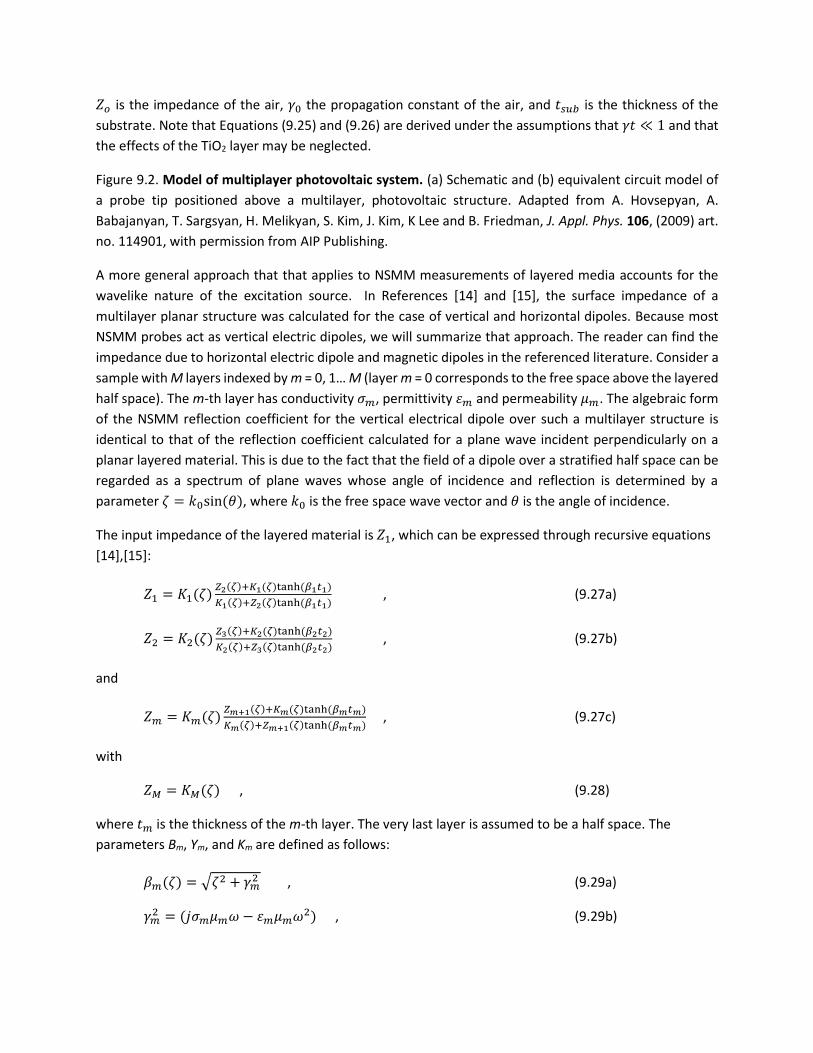
𝑍𝑜 is the impedance of the air, 𝛾0 the propagation constant of the air, and 𝑡𝑠𝑢𝑏 is the thickness of the
substrate. Note that Equations (9.25) and (9.26) are derived under the assumptions that 𝛾𝑡 ≪ 1 and that
the effects of the TiO2 layer may be neglected.
Figure 9.2. Model of multiplayer photovoltaic system. (a) Schematic and (b) equivalent circuit model of
a probe tip positioned above a multilayer, photovoltaic structure. Adapted from A. Hovsepyan, A.
Babajanyan, T. Sargsyan, H. Melikyan, S. Kim, J. Kim, K Lee and B. Friedman, J. Appl. Phys. 106, (2009) art.
no. 114901, with permission from AIP Publishing.
A more general approach that that applies to NSMM measurements of layered media accounts for the
wavelike nature of the excitation source. In References [14] and [15], the surface impedance of a
multilayer planar structure was calculated for the case of vertical and horizontal dipoles. Because most
NSMM probes act as vertical electric dipoles, we will summarize that approach. The reader can find the
impedance due to horizontal electric dipole and magnetic dipoles in the referenced literature. Consider a
sample with M layers indexed by m = 0, 1… M (layer m = 0 corresponds to the free space above the layered
half space). The m-th layer has conductivity 𝜎𝑚, permittivity 휀𝑚 and permeability 𝜇𝑚. The algebraic form
of the NSMM reflection coefficient for the vertical electrical dipole over such a multilayer structure is
identical to that of the reflection coefficient calculated for a plane wave incident perpendicularly on a
planar layered material. This is due to the fact that the field of a dipole over a stratified half space can be
regarded as a spectrum of plane waves whose angle of incidence and reflection is determined by a
parameter 휁 = 𝑘0sin (𝜃), where 𝑘0 is the free space wave vector and 𝜃 is the angle of incidence.
The input impedance of the layered material is 𝑍1, which can be expressed through recursive equations
[14],[15]:
𝑍1 = 𝐾1(휁)𝑍2( )+𝐾1( )tanh (𝛽1𝑡1)
𝐾1( )+𝑍2( )tanh (𝛽1𝑡1) , (9.27a)
𝑍2 = 𝐾2(휁)𝑍3( )+𝐾2( )tanh (𝛽2𝑡2)
𝐾2( )+𝑍3( )tanh (𝛽2𝑡2) , (9.27b)
and
𝑍𝑚 = 𝐾𝑚(휁)𝑍𝑚+1( )+𝐾𝑚( )tanh (𝛽𝑚𝑡𝑚)
𝐾𝑚( )+𝑍𝑚+1( )tanh (𝛽𝑚𝑡𝑚) , (9.27c)
with
𝑍𝑀 = 𝐾𝑀(휁) , (9.28)
where 𝑡𝑚 is the thickness of the m-th layer. The very last layer is assumed to be a half space. The
parameters Bm, Ym, and Km are defined as follows:
𝛽𝑚(휁) = √휁2 + 𝛾𝑚2 , (9.29a)
𝛾𝑚2 = (𝑗𝜎𝑚𝜇𝑚𝜔 − 휀𝑚𝜇𝑚𝜔2) , (9.29b)

𝐾𝑚(휁) =𝛽𝑚( )
𝜎𝑚+𝑗𝜔 𝑚 . (9.29c)
The generalized reflection coefficient is
Γ(휁) =𝐾0( )−𝑍1( )
𝐾0( )+𝑍1( ) . (9.30)
This solution is reminiscent of the one-port reflection coefficient derived for a transmission line [4],[14].
When the incident plane wave is perpendicular to the surface, 𝜃 = 0, 𝛽𝑚 = 𝛾𝑚 and 𝐾𝑚 = 𝑍𝑚. In the limit
where the multilayer structure consists of very thin layers, the equations for the impedance and reflection
coefficient of the layered medium are reduced to ordinary differential equations of the so-called Ricatti
form that can be solved as an initial value problem [16].
9.3. Resonant cavity models and methods
9.3.1 Resonant-cavity-based, near-field scanning microwave microscopy
Up to now, we have described the interaction of the tip and the sample by use of a sample impedance.
Alternatively, we can treat the whole NSMM system as a specialized transmission cavity [17]. Such a
treatment of NSMM was first introduced in Reference [18] and many NSMM instruments intended for
material characterization rely on an engineered resonant system inserted between a network analyzer
and the tip-sample junction [19]-[21]. Some resonant NSMM implementations operate in a linear regime
[17], while others operate in a nonlinear regime [22],[23].
In order to understand resonant NSMM measurements, it is necessary to understand how the tip-sample
system can be represented by a load on a resonant circuit. There are several lumped element circuit
models that represent a resonant circuit connected to the NSMM probe tip. For example, in Reference
[24], the coaxial resonator circuit is modeled as a sixth order LCR notch filter, while in Reference [18] the
resonator circuit is modeled by a simple series or parallel RLC circuit. Here, we follow the approach of
Reference [17], as shown in Fig. 9.3. The equivalent lumped element circuit of a resonator is coupled to a
source as well as the tip-sample junction. The junction is represented by a lumped element circuit, as
previously introduced in Fig. 9.1. The application of this model depends upon which method is used to
measure the reflection coefficient Γ from the NSMM (In some places, the reflection coefficient is
alternately referred to as S11 and we will use both notations).
There are two common measurement techniques. In the first technique, the source frequency is swept in
a narrow range around the resonance frequency and Γ is measured as a function of frequency for each
probe position. In the second technique, at each probe position, Γ is measured at a single, constant
frequency chosen to be near, but not equal to the resonant frequency. Each of these techniques has
advantages and disadvantages. The former technique provides a richer set of measurement data, but
latter is simpler and faster. Thus, the constant frequency technique is the more common approach,
particularly in commercial NSMMs.
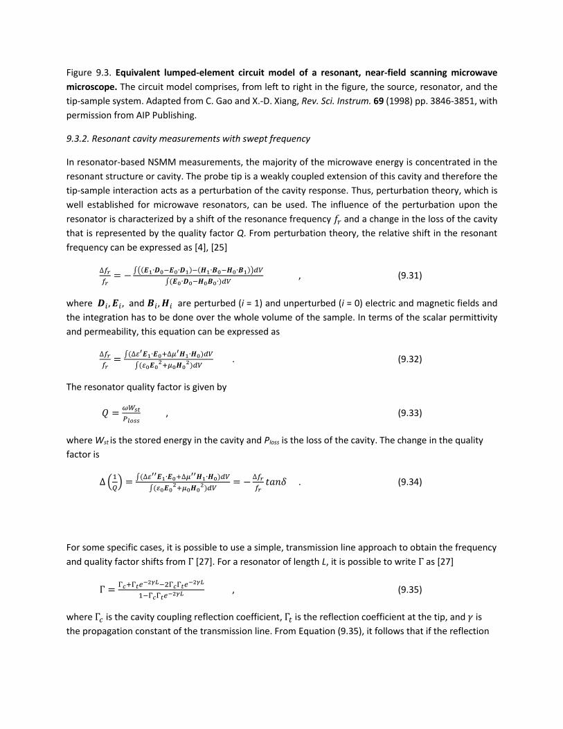
Figure 9.3. Equivalent lumped-element circuit model of a resonant, near-field scanning microwave
microscope. The circuit model comprises, from left to right in the figure, the source, resonator, and the
tip-sample system. Adapted from C. Gao and X.-D. Xiang, Rev. Sci. Instrum. 69 (1998) pp. 3846-3851, with
permission from AIP Publishing.
9.3.2. Resonant cavity measurements with swept frequency
In resonator-based NSMM measurements, the majority of the microwave energy is concentrated in the
resonant structure or cavity. The probe tip is a weakly coupled extension of this cavity and therefore the
tip-sample interaction acts as a perturbation of the cavity response. Thus, perturbation theory, which is
well established for microwave resonators, can be used. The influence of the perturbation upon the
resonator is characterized by a shift of the resonance frequency 𝑓𝑟 and a change in the loss of the cavity
that is represented by the quality factor Q. From perturbation theory, the relative shift in the resonant
frequency can be expressed as [4], [25]
∆𝑓𝑟
𝑓𝑟= −
∫((𝑬1∙𝑫0−𝑬0∙𝑫1)−(𝑯1∙𝑩0−𝑯0∙𝑩1))𝑑𝑉
∫(𝑬0∙𝑫0−𝑯0𝑩0∙)𝑑𝑉 , (9.31)
where 𝑫𝑖, 𝑬𝑖 , and 𝑩𝑖, 𝑯𝑖 are perturbed (i = 1) and unperturbed (i = 0) electric and magnetic fields and
the integration has to be done over the whole volume of the sample. In terms of the scalar permittivity
and permeability, this equation can be expressed as
∆𝑓𝑟
𝑓𝑟=
∫(∆ ′𝑬1∙𝑬0+∆𝜇′𝑯1∙𝑯0)𝑑𝑉
∫( 0𝑬02+𝜇0𝑯0
2)𝑑𝑉 . (9.32)
The resonator quality factor is given by
𝑄 =𝜔𝑊𝑠𝑡
𝑃𝑙𝑜𝑠𝑠 , (9.33)
where Wst is the stored energy in the cavity and Ploss is the loss of the cavity. The change in the quality
factor is
∆ (1
𝑄) =
∫(∆ ′′𝑬1∙𝑬0+∆𝜇′′𝑯1∙𝑯0)𝑑𝑉
∫( 0𝑬02+𝜇0𝑯0
2)𝑑𝑉= −
∆𝑓𝑟
𝑓𝑟𝑡𝑎𝑛𝛿 . (9.34)
For some specific cases, it is possible to use a simple, transmission line approach to obtain the frequency
and quality factor shifts from Γ [27]. For a resonator of length L, it is possible to write Γ as [27]
Γ =Γ𝑐+Γ𝑡𝑒−2𝛾𝐿−2Γ𝑐Γ𝑡𝑒−2𝛾𝐿
1−Γ𝑐Γ𝑡𝑒−2𝛾𝐿 , (9.35)
where Γ𝑐 is the cavity coupling reflection coefficient, Γ𝑡 is the reflection coefficient at the tip, and 𝛾 is
the propagation constant of the transmission line. From Equation (9.35), it follows that if the reflection
coefficient is only weakly dependent on frequency, i.e. if 𝑓0𝜕|Γ𝑐,𝑡| 𝜕𝜔⁄ ≪ 1 𝑎𝑛𝑑 𝑓0𝜕(argΓ𝑐,𝑡) 𝜕𝜔⁄ ≪ 1 ,
then [26]
Δ𝑓𝑟 ≈1
2𝜋
∑ 𝜕𝜑 𝜕𝑐𝑖⁄𝑖
𝜕𝜑 𝜕𝜔⁄=
1
2𝜋𝑓0 ∑
𝜕𝑎𝑟𝑔(Γ𝑡)
𝜕𝑐𝑥𝑑𝑐𝑥𝑥 , (9.36)
where 𝜑 = arg (Γ𝑐Γ𝑡𝑒−2𝛾𝐿) and f0 is the unperturbed, fundamental resonance frequency of the resonator.
The circuit variable set {𝑐𝑥} = {𝐶𝑠𝑡𝑟, 𝐶𝑐𝑝𝑙, 𝑍𝑠(𝐶𝑠, 𝑅𝑠)} is drawn from the equivalent circuit in Fig. 9.3 or
other equivalent circuits. The circuit variables are directly related to the change of the resonance
frequency in the experiment. If one can neglect the tip resistance Rt, Equation (9.36) can be simplified to
Δ𝑓𝑟
𝑓𝑟≈ −2𝑍0𝑓0 ∑
𝜕𝐶𝑡
𝜕𝑐𝑖𝑑𝑖 𝑐𝑖 . (9.37)
Ct is the effective tip capacitance derived from the given lumped element circuit. Under the same
assumption, the change of the quality factor can be expressed as [26]
∆ (1
𝑄) =
4
𝜔𝑓0𝑍0∆𝐺 . (9.38)
∆𝐺 is the change in the parallel conductance of the sample (defined by the sample impedance
𝑍𝑠(𝑅𝑠, 𝐶𝑠)) from Fig. 9.3 and represents the changes in the loss within the sample. Note that 𝐺𝑝 𝜔⁄
directly determines the losses in the sample.
The exact forms of the solutions to Equations (9.31), (9.32), and (9.34) depend on the geometry of the
system, material properties and boundary conditions. Therefore, we will not include here a derivation of
general analytic solutions to those equations in terms of a Green’s function or other formulation.
Experimentally, the local permittivity and permeability may be determined by use of Equations (9.31),
(9.32), and (9.34), as follows. The frequency shift, i.e. the left hand side of Equations (9.31) and (9.32), is
obtained from measurement of the reflection coefficient during a frequency sweep around the resonance
frequency. To obtain the shift, this measurement must be carried out both when the resonator is
unperturbed (far from the sample) and when the resonator is loaded (near the sample). The measurement
of the frequency shift of the cavity with respect to the unperturbed resonance frequency can be obtained
directly.
Obtaining the shift in the cavity quality factor ∆𝑄 from the measurements can be confusing. Intuitively,
one might assume the quality factor of the resonant cavity is obtained directly from the fitting the
observed frequency dependence in the vicinity of the resonant frequency. This is incorrect and therefore
we will spend some time to define the correct approach following the procedure described in Reference
[28]. Considering the circuit model of the resonant cavity in Fig. 9.3, it is possible to define an external
quality factor QE associated with the power dissipation due to coupling of the cavity to the external
circuitry (e.g. the iris in waveguide cavities). It is also possible to define a quality factor QV associated with
the dissipation within the cavity volume (e.g. the combined cavity and sample dissipation volumes). The
overall QL factor of the cavity then can be expressed as
1
𝑄𝐿=
1
𝑄𝐸+
1
𝑄𝑉 . (9.39)
It is useful to introduce reduced parameters 𝛿𝐸 = 𝑄𝐸∆𝜔, 𝛿𝑉 = 𝑄𝑉∆𝜔, and 𝛿𝐿 = 𝑄𝐿∆𝜔, with ∆𝜔=𝜔
𝜔𝑟−
𝜔𝑟
𝜔 . In addition, by Introducing 𝛽 = 𝑄𝑉 𝑄𝐸 = (
1∓𝑆11𝑟
1±𝑆11𝑟)⁄ ,where S11r is the reflection coefficient at
resonance frequency, as a coupling coefficient of the cavity, it is possible to relate the reduced
parameters to the measured reflection coefficient 𝑆11(𝜔) as [28]
𝛿𝑉 = ±√(1+𝛽)2𝑆11
2 −(1−𝛽)2
1−𝑆112 . (9.40)
The ± sign in Equation (9.40) is determined by sign of ∆𝜔 which is negative for 𝜔𝑟 < 𝜔 and positive for
𝜔𝑟 > 𝜔. The other reduced parameters can be determined from 𝛿𝑉 by 𝛿𝐸 = 𝛿𝑉 𝛽⁄ and 𝛿𝐿 = 𝛿𝑉 (1 + 𝛽)⁄ .
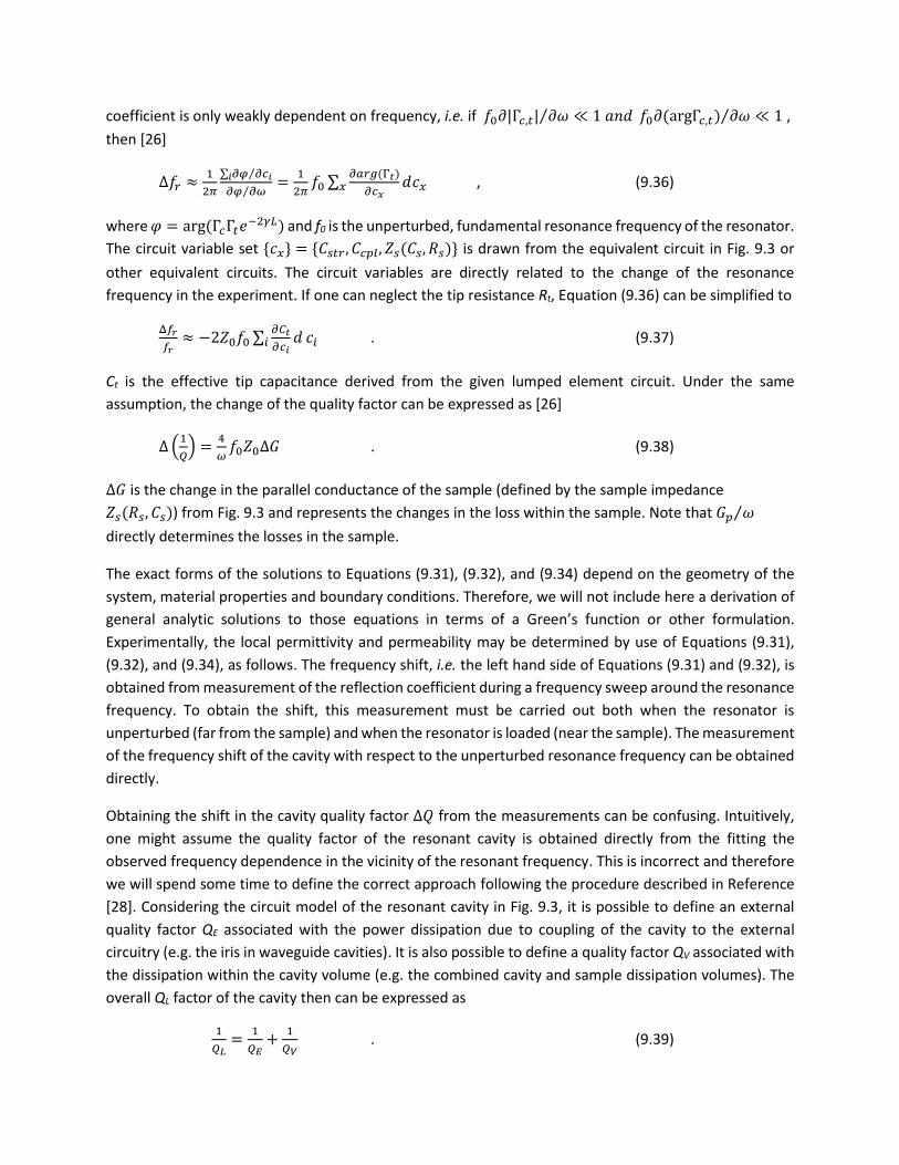
Plotting the reduced parameters as a function of ∆𝜔 and obtaining a linear fit yields QE, QV, and QL. An
example of the measured frequency dependence of the reflection coefficient and the deduction of the
quality factors is shown in Fig. 9.4. Specifically, Fig. 9.4(a) shows the frequency-dependence of the
reflection coefficient and Fig. 9.4(b) shows the parameter 𝛿𝑉 as a function of ∆𝜔. It is possible to use a
similar procedure to obtain the quality factor for a transmission cavity in which S21 is measured.
Figure 9.4. Obtaining the cavity quality factor from resonant, near-field scanning microwave microscope
measurements. (a) A comparison of measured (solid grey line) and calculated (dashed black line)
reflection coefficients as a function of frequency. (b) The experimental reduced parameter 𝛿𝑉 (solid grey
line) is determined from the measured reflection coefficient. A linear fit (dashed black line) to the
experimental data provides the quality factor QV associated with the dissipation within the cavity volume.
Further, the fitted values of 𝛿𝑉 are used to find the calculated reflection coefficient in (a).
NSMM-based measurements of the complex permittivity of bulk materials provide a practical example of
material characterization through measurement of the frequency shift and change in the quality factor
[29]. We consider specific examples of frequency-swept measurements that reveals a number of issues
that are important for quantitative characterization of material properties. A typical experimental
configuration of an NSMM resonator is described in Reference [17]. The bulk SUTs studied therein include
dielectrics, semiconductors and metals. The experimental data confirmed that the shift of the resonance
frequency is most sensitive to the tip-sample coupling capacitance CCpl and the capacitive contribution to
the sample impedance Zs (See Fig. 9.3), while the change of the quality factor is most sensitive to the
resistive contribution to Zs (Although, in general both shifts are functions of CCpl and the total sample
impedance Zs).
In the specific examples of fused silica and silicon, the shift in the resonance frequency and the quality
factor were measured by use of frequency-swept measurements at each height in the range from 0.1 to
1000 m above the sample. The experimental results are shown in Fig. 9.5 where ∆𝑓 𝑓0⁄ is plotted
against 𝑄/𝑄0. The unperturbed values of f0 and Q0 of the unloaded resonator are measured at the height
of 1000 m. As seen in Fig. 9.5, there is a significant, height-dependent frequency shift but little change

in quality factor for the fused silica, as expected for a low loss material. For the silicon, in which the loss is
significantly higher, there is a significant change in both the quality factor and the resonant frequency. To
extract the material properties from the experimentally observed dependences for dielectric and
semiconducting materials, the coupling capacitance can be successfully modeled by the quasi-static image
charge method discussed in Chapter 7. The sample properties can be modeled by use of the lumped
element approach, as described in Equations (9.16) through (9.19). In this example, when the sample is
modeled as a series RLC circuit the input impedance of the resonator is [27]
𝑍𝑖𝑛 = 𝑅𝑟𝑒𝑠(1 + 2𝑗(𝑄 ∆𝑓 𝑓0)⁄ , (9.41)
where Rres is the series resistance of the resonator equivalent circuit.
Figure 9.5. NSMM measurements of silicon and fused silica. The normalized shift of the resonance
frequency is shown as a function of the change in the resonator quality factor for bulk silicon (open circles)
and bulk fused silica (open triangles). Fitted curves for a quasistatic model are shown as solid lines for
both samples. Reprinted from A. Imtiaz, T. Baldwin, H. T. Nembach, T. M. Wallis and P. Kabos, Appl. Phys.
Lett. 90 (2007) art. no. 243105, with permission from AIP Publishing.
There are several different ways to visualize height-dependent NSMM measurements, each of which
brings out different features. In general, different materials with different complex permittivity values will
present different loads to the resonator. Data plotted with ∆𝑓 as a function of Q, as in Fig. 9.5 visually
distinguish different classes of materials – dielectrics, semiconductors, and metals - based on differences
in the loss. By contrast, plotting Q as a function of height offers little distinction between the respective
responses of metal and dielectrics. Finally, a plot of the product (∆𝑓 𝑓0)⁄ (𝑄 𝑄0)⁄ versus height highlights
the capacitive coupling to the sample load.
A pure quasi-static model of the tip-sample interaction fails for metals. In particular, it is necessary to
include a calculation of the near field antenna impedance as it is brought close to a metal surface, as
discussed in Chapter 8. The reason for this is that there is non-negligible resistive loss in the antenna
(probe tip) as it is brought close to the metal surface.
9.3.3. Calibration, uncertainty, and sensitivity
To model and extract the correct material properties, an unknown critical parameter - the effective tip
diameter dTip - must be obtained. One technique to find dTip is via the calibration procedures discussed in
Chapter 8. Another possibility is to use a low loss dielectric with known permittivity as a calibration
sample. This is essentially a simplified calibration procedure for height-dependent NSMM of bulk
materials. To obtain the effective tip diameter from the measured dependence of ∆𝑓 versus height for
the known, low-loss calibration material, one need only fit that data with the single fitting parameter dTip.
Another calibration approach is presented in Reference [30], in which the permittivity of a thin film was
obtained. The experimental system comprised a loop-coupled cavity operating as a transmission
resonator and a probe tip protruding from the bottom of that cavity. The system was calibrated by
measuring three reference samples: magnesium oxide, neodymium gallate and yttrium-stabilized
zirconia. The permittivity of the reference samples was known from measurements made by use of a split
post resonator technique. The transmission coefficient of the cavity resonator S21 was measured both for
standard samples as well as the thin film at two frequencies: 1.8 GHz and its third harmonic 4.4 GHz. To
reduce statistical error, measurements were made at different positions on the film. After these
measurements the film was patterned with a coplanar waveguide to measure its permittivity through a
complementary method. The measured transmission coefficients were fitted to the equation [30]
𝑆21(𝑓) = 𝑆21𝐿 +𝑆21(𝑓0)
1+𝑗𝑄𝐿∆𝜔𝑒𝑗𝜙; ∆𝜔 =
𝑓2−𝑓02
𝑓2 , (9.42)
where 𝑆21𝐿 is the non-resonant leakage between the ports. The phase shift 𝜙 is introduced due to the
fact that the measurement ports are physically separated from the coupling loops. 𝑆21(𝑓0) is the
transmission coefficient at resonance. The data can be subsequently processed following the perturbation
approach introduced in Equations (9.31) through (9.34).
An analysis of the measurement uncertainty is critical for any quantitative measurements of materials
with NSMM. In this case, the total uncertainty was estimated from statistical uncertainties in the
measurement of tip diameter dtip, film thickness t, calibration constant A and normalized frequency shift
as
𝜎(휀𝑓) = [(𝛿휀𝑓
𝛿 (𝑑𝑡𝑖𝑝 2)⁄)
2
𝜎(𝑑𝑡𝑖𝑝 2⁄ )2 + (𝛿휀𝑓
𝛿𝑡)
2
𝜎(𝑡)2 + (𝛿휀𝑓
𝛿𝐴)
2
𝜎(𝐴)2 + (𝛿휀𝑓
𝛿(∆𝑓/𝑓′))
2
𝜎(∆𝑓/𝑓′)2]
12
(9.43)
where 휀𝑓 is the permittivity of the film. The differential terms can be obtained from analytical expressions
of the frequency shift derived from models of the tip sample interaction, such as the charge image model
[17].
The sensitivity of NSMM for measurement impedances is [23]
𝑆𝑓 =𝑔𝑠𝜔0
4𝜋
𝐶𝑐2
𝐶0(𝐶𝑐+𝐶𝑠)2 , (9.44)
where 𝑔𝑠 = 𝐴𝑒𝑓𝑓 (𝜉𝑠)⁄ , 𝐴𝑒𝑓𝑓 and corresponds to the effective tip area, 𝜉𝑠 is the decay length of the
evanescent wave, 𝐶𝑐 is the coupling capacitance, 𝐶0 is the capacitance of the equivalent circuit of the
resonator, and 𝜔0 is the unloaded, radial resonance frequency. To distinguish between the regions of
different permittivity it is necessary to fulfill the condition
∆= (
𝑉𝑛(𝑟𝑚𝑠)
𝑉𝑖𝑛) /(𝑆𝑓𝑆𝑟휀) (9.45)

with 𝑆𝑟 defined as [22]
𝑆𝑟 =𝑑𝑆11
𝑑𝜔≈
𝑄′
𝜔0′ (1 −
∆𝜔
𝜔0′ ) ; ∆𝜔 = 𝜔 − 𝜔0
′ . (9.46)
Q’ and 𝜔0′ are the perturbed quality factor and resonance frequency of the resonator due to tip-sample
interaction, 𝑉𝑛(𝑟𝑚𝑠) = √(4𝑘𝐵𝑇𝐵𝑅) is the rms value of the noise voltage generated by resistance R at
temperature T, 𝑘𝐵 is Boltzmann constant, B is the bandwidth of the system, and 𝑉𝑖𝑛 is the probe input
voltage.
9.3.4 Resonant cavity measurements of semiconductors
Semiconductors are foundational for nanoelectronic applications. As the dimensions of semiconductors
are scaled to the nanometer range, important questions arise about the applicability of standard
semiconductor device theories at these scales. Moreover, such scaled systems are inherently more
sensitive to the effects of interfaces and defects. Thus, scanning probe techniques are vital experimental
tools for spatially-resolved characterization of these materials. NSMM is but one of many different
scanning probe techniques used for the local, nanoscale characterization of semiconducting materials
[32], as we will discuss further in Chapter 11.
When a metal NSMM probe tip is in contact with a native or deposited oxide layer on a semiconductor
SUT, the tip-sample interface may be treated as a metal-oxide-semiconductor (MOS) system. In order to
model the MOS system, a number of modifications must be made to the model shown in Fig. 9.3. For the
tip sample assembly, a nanoscale, parallel plate MOS capacitor with effective tip diameter can be used in
most cases as a first approximation. As the tip is in a contact with the surface of the sample, there is no
need to model the coupling capacitance separately from the sample response. In contact mode, the field
is concentrated under the tip and the stray capacitance can be incorporated into the effective tip
diameter. This simplifies the sample model, e.g., to a series connection of the oxide and sample
capacitances [24]. To further simplify the model, charges at the oxide-semiconductor interface may be
neglected. It is important to remember that any 50 Ohm shunt resistor that is sometimes present in
commercial system configurations has to be included in the model.
Experimentally, a DC bias 𝑉𝑡𝑖𝑝 is often applied to the probe tip and varied systematically throughout the
measurements. In the case of silicon samples, it has been shown that the sample response under such a
varying tip bias can be effectively modeled by use of standard MOS theories [33]. As 𝑉𝑡𝑖𝑝 is varied, the
resonant circuit is perturbed due to changes in the depletion within the semiconductor, resulting in a
change in the reflection coefficient measured by the NSMM. If a small, low frequency voltage is added to
𝑉𝑡𝑖𝑝, then the derivative 𝑑𝑆11 𝑑𝑉𝑡𝑖𝑝⁄ may be measured simultaneously by use of a lockin technique. Just
as macroscopic capacitance-voltage curves provide an avenue to measure dopant concentration in
semiconductors, local, tip-bias-dependent NSMM measurements provide a way to calibrate the local
dopant concentration and quantify their distribution throughout the sample [32].
This requires a calibration sample with regions of known dopant concentration NA. An ideal calibration
sample has a flat surface with no significant topographic variation such that any changes in the measured
reflection coefficient are due to materials contrast. One particular implementation, to which we will refer
below, comprises a series of regions of variably-doped silicon, each with a different dopant concentration.
Each region is a 1.5 m – wide strip, such that the materials contrast appears as a series of parallel stripes.
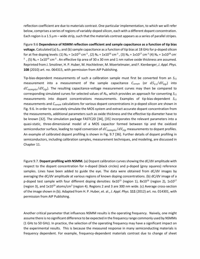
Figure 9.6 Dependence of NSMM reflection coefficient and sample capacitance as a function of tip bias
voltage. Calculated (a) S11 and (b) sample capacitance as a function of tip bias at 18 GHz for p-doped silicon
for at five doping levels: (1) NA = 1x1015 cm-3 , (2) NA = 1x1016 cm-3 , (3) NA = 1x1017 cm-3 (4) NA = 1x1018 cm-
3 , (5) NA = 1x1019 cm-3 . An effective tip area of 30 x 30 nm and 1 nm native oxide thickness are assumed.
Reprinted from J. Smoliner, H. P. Huber, M. Hochleitner, M. Moertelmaier, and F. Kienberger, J. Appl. Phys.
108 (2010) art. no. 064315, with permission from AIP Publishing.
Tip-bias-dependent measurements of such a calibration sample must first be converted from an S11
measurement into a measurement of the sample capacitance Csample (or 𝑑𝑆11 𝑑𝑉𝑡𝑖𝑝⁄ ) into
𝑑𝐶𝑠𝑎𝑚𝑝𝑙𝑒 𝑑𝑉𝑡𝑖𝑝⁄ ). The resulting capacitance-voltage measurement curves may then be compared to
corresponding simulated curves for selected values of NA, which provides an approach for converting S11
measurements into dopant concentrations measurements. Examples of tip-bias-dependent S11
measurements and Csample calculations for various dopant concentrations in p-doped silicon are shown in
Fig. 9.6. In order to accurately simulate the MOS system and extract accurate dopant concentration from
the measurements, additional parameters such as oxide thickness and the effective tip diameter have to
be known [32]. The simulation package FASTC2D [34], [35] incorporates the relevant parameters into a
quasi-static, three-dimensional model of a MOS capacitor formed between tip and the oxidized
semiconductor surface, leading to rapid conversion of 𝑑𝐶𝑠𝑎𝑚𝑝𝑙𝑒 𝑑𝑉𝑡𝑖𝑝⁄ measurements to dopant profiles.
An example of calibrated dopant profiling is shown in Fig. 9.7 [36]. Further details of dopant profiling in
semiconductors, including calibration samples, measurement techniques, and modeling, are discussed in
Chapter 11.
Figure 9.7. Dopant profiling with NSMM. (a) Dopant calibration curves showing the dC/dV amplitude with
respect to the dopant concentration for n-doped (black circles) and p-doped (grey squares) reference
samples. Lines have been added to guide the eye. The data were obtained from dC/dV images by
averaging the dC/dV amplitude at various regions of known doping concentrations. (b) dC/dV image of a
p-doped test sample with four different doping densities: 6x10¹⁵ (region 1), 8x10¹⁶ (region 2), 1x10¹⁷
(region 3), and 1x10¹⁹ atoms/cm3 (region 4). Regions 2 and 3 are 300 nm wide. (c) Average cross-section
of the image shown in (b). Adapted from H. P. Huber, et. al., J. Appl. Phys. 111 (2012) art. no. 014301, with
permission from AIP Publishing.
Another critical parameter that influences NSMM results is the operating frequency. Naively, one might
assume there is no significant difference to be expected in the frequency range commonly used by NSMMs
(1 GHz to 50 GHz). In practice, the selection of the operating frequency may have a significant impact on
the experimental results. This is because the measured response in many semiconducting materials is
frequency dependent. For example, frequency-dependent materials contrast due to change of sheet

resistance was observed in boron-doped silicon [37]. A more systematic investigation of the influence of
the frequency was carried out on the “striped” calibration sample described above [32],[38]. In order to
compare results at different operating frequencies, a phase shifter is inserted into the microwave signal
path between the VNA and the NSMM resonator, as illustrated in Fig. 9.8(a). With 𝑉𝑡𝑖𝑝 equal to zero, at
each operating frequency, the phase shifter is used to tune the reactance of the input impedance such
that sample the reflection coefficient has a magnitude of about – 50 dB. In Fig. 9.8(b), the vertical lines in
the NSMM image delineate areas of different p-type dopant concentrations. The horizontal, black, dashed
lines represent changes in the DC tip bias. The series of DC tip biases is denoted at the right edge of the
image. For this image acquired at 5 GHz, there is increased NSMM sensitivity in the stripe with a doping
concentration of 1017 cm3 while the NSMM contrast for the other doping concentrations is suppressed.
As the operating frequency is switched to other values - 2.3 GHZ, 9.6 GHz, 12.6 GHz and 17.9 GHz –
increased sensitivity is observed in different ranges of dopant concentrations. Fig. 9.8 (d) shows a
calculation of the frequency-dependent input impedance for a given dopant concentration. The maximum
in the input impedance represents an optimal operating frequency or “selection frequency.” Fig. 9.8 (c)
shows calculated selection frequencies as a function of the doping concentration. The experimental
results are in reasonable agreement with these theoretical predictions and generally support the
application of standard MOS theory to such measurements. These measurements underscore the
significant potential of NSMM as a broadband tool that reveals physical behavior that can’t be observed
via single-frequency measurements, albeit with restrictions that arise from the fact that the
experimentally utilized frequencies are constrained by the intrinsic response of the NSMM resonator.
Figure 9.8. Frequency dependent sensitivity of NSMM. (a) Schematic of the AFM-based NSMM with the
phase shifter. (b) An image of d(S11)/dV, acquired at 5 GHz, illustrating the structure of the sample. Solid
white vertical lines delineate the different doped regions: A = bulk silicon, B = 1016 cm-3, C = 1017 cm-3, D=
1018 cm-3, E = 1019 cm-3, and F =1020 cm-3. The dashed black lines demarcate regions of various applied tip
bias voltages. (c) Calculated selection frequency vs. doping concentration (solid lines) for 2.3 GHz, 5.0
GHz, 9.6 GHz, 12.6 GHz and 17.9 GHz. The rectangles represent the measured concentrations from the
highlighted areas at a given frequency. (d) Calculated input impedance vs. frequency. The operating
frequency 12.6 GHz is most sensitive to concentrations near 1017 cm-3, while 9.6 GHz and 17.9 GHz are
most sensitive to 1016 cm-3 and 1018 cm-3, respectively. Reprinted from A. Imtiaz, T. M. Wallis, S.-H. Lim,
H. Tanbakuchi, H.-P. Huber, A. Hornung, P. Hinterdorfer, J. Smoliner, F. Kienberger, and P. Kabos, J. Appl.
Phys. 111 (2012) art. no. 093727, with permission from AIP Publishing.
The observed, frequency-dependent response of NSMM is attributed to the underlying physics within the
sample as described by standard MOS diode theory [33], [39]. From MOS diode theory the space-charge
density may be calculated as a function of the surface potential defined with respect to intrinsic Fermi
level. Knowing the space charge density, it is possible to solve for the surface charge density Qs(s), where
s is the surface potential. Next it is necessary to calculate the depletion layer capacitance 𝐶𝑑𝑒𝑝𝑙 =
𝜕𝑄𝑠 𝜕𝜓𝑠⁄ , which is a function of the tip-bias voltage. In the NSMM measurements, one has to consider
only high frequency branch of this capacitance. The microscope is sensitive to changes in the series
combination of the oxide and 𝐶𝑑𝑒𝑝𝑙 capacitances. In addition, incident microwave power is dissipated in
the sample through the surface resistance Rsurf, which is given by
𝑅𝑠𝑢𝑟𝑓 = 𝜌𝑠/𝛿𝑠𝑑 , (9.47)
where 𝜌𝑠 is the resistivity of the locally doped region and 𝛿𝑠𝑑 = √𝜌𝑠 𝜇0𝜋𝑓⁄ is the skin depth of the
penetrating microwave field. This resistance is in series with the sheet resistance of the semiconductor
𝑅𝑠ℎ = 𝜌𝑠/𝑑𝑒𝑓𝑓 , (9.48)
where 𝑑𝑒𝑓𝑓 is an effective length scale corresponding roughly to the distance from the top of the sample
to the nearest grounding conductor. This optimal NSMM operating frequency, or “selection frequency,”
is inversely proportional to the selection time constant
𝜏𝑠𝑒𝑙 = 𝜉(𝑅𝑠𝑢𝑟𝑓+𝑅𝑠ℎ)
𝐶𝑡𝑜𝑡 , (9.49)
where
𝐶𝑡𝑜𝑡 =𝐶𝑑𝑒𝑝𝑙𝐶𝑜𝑥
𝐶𝑑𝑒𝑝𝑙+𝐶𝑜𝑥 . (9.50)
The parameter 𝜉 is dimensionless and is proportional to (4𝛿𝑠𝑑
𝑑𝑡𝑖𝑝)
2
. Note that NSMM measurements in the
frequency range between 1 GHz and 50 GHz of n-doped samples show no frequency dependence. This is
attributed to the fact that the mobility of the holes in a p-type sample is about ten times smaller than the
mobility of electrons in n-type samples. Thus p-type samples will display a higher resistivity and in turn a
higher 𝜏𝑠𝑒𝑙 relative to n-type samples. In order to observe frequency-dependent contrast in an n-type
sample, the NSMM operating frequency must be significantly higher than 50 GHz.
9.3.5. Nonlinear dielectric microscopy of materials
Another application area for resonant NSMM is the imaging of spontaneous polarization of ferroelectric
materials based on measurement of the spatial variation of the nonlinear dielectric constant [40]-[44].
The design, shown in Fig. 9.9, is capable of nanometer resolution. The microscope’s signal path consists
of an LC resonator in series with a needle probe. The operating frequency of the probe lies in the range
between 1 GHz and 6 GHz. An oscillating electric field
𝑣(𝑡) = 𝑉𝑐𝑜𝑠(𝜔𝑝𝑡) (9.51)
is applied in addition to the applied field between the tip and the back electrode under the sample,
resulting in a frequency-modulated signal. The nonlinear response of the sample volume beneath the tip
to this field leads to a modulation of the sample capacitance ∆𝐶𝑠(𝑡) that in turn leads to a modulation of
the probe oscillating frequency. After demodulation, a lock-in amplifier is used to record the capacitance
variation.

Figure 9.9. Schematic diagram of scanning nonlinear dielectric microscope. Reprinted from Y. Cho, S.
Kazuta, and K. Matsuura, Appl. Phys. Lett. 75 (1999) pp.2833-2835, with permission from AIP Publishing.
The voltage-dependent capacitance variation can be quantitatively related to the local, nonlinear
dielectric constant as follows. The tip-sample capacitance as a function of the voltage 𝑣 can be expanded
in a Taylor series
𝐶𝑠(𝑡) = 𝐶𝑠0 + (𝑑𝐶𝑠
𝑑𝑣) 𝑣 +
1
2(
𝑑2𝐶𝑠
𝑑𝑣2 ) 𝑣2 +1
6(
𝑑3𝐶𝑠
𝑑𝑣3 ) 𝑣3 + ⋯ (9.52)
The displacement can be expressed as a function of the electric field [44]
𝑫 = 𝑷𝒔 + [𝜺(𝟐)] ∙ 𝑬 +1
2[𝜺(𝟑)]: 𝑬𝟐 +
𝟏
𝟔[𝜺(𝟒)]: 𝑬𝟑 +
1
24[𝜺(𝟓)]: 𝑬𝟒 + ⋯ , (9.53)
where Ps is a spontaneous polarization. The variables [𝜺(𝒊)] i= 2,3,.. are permittivity tensors. For i=2, this
represents the linear permittivity and is a second rank tensor. For higher values of the index i, the
corresponding tensors of increasing rank represent the nonlinear permittivity. The odd, nonlinear terms
in (9.53) are sensitive to polarization direction. The ratio of the change in the capacitance ∆𝐶𝑠(𝑡) =
𝐶𝑠(𝑡) − 𝐶𝑠0 to the static value of the capacitance can be expressed (for isotropic media) as [44]
∆𝐶𝑠(𝑡)
𝐶𝑠0≈
(3)
(2)𝐸𝑝 cos(𝜔𝑝𝑡) +
1
4
(4)
(2)𝐸𝑝
2 cos(2𝜔𝑝𝑡) +1
24
(5)
(2)𝐸𝑝
3 cos(3𝜔𝑝𝑡) + ⋯ . (9.54)
where ωp is the radial lock-in reference frequency.
An atomic-scale image acquired from the 휀(4) nonlinear dielectric signal is shown in Fig. 9.10. The well-
known arrangement of silicon adatoms in a reconstructed Si(111)-7x7 surface is clearly discernable.
Figure 9.10 Atomic resolution image obtained by use of nonlinear dielectric microscopy [42].
Topography of a reconstructed Si(111)-7x7 surface obtained from the 휀(4) signal in scanning nonlinear
dielectric microscope. [42] © IOP Publishing. Adapted with permission. All rights reserved.
9.4. Measurements of thin films and low dimensional materials
9.4.1 Materials for radio-frequency nanoelectronics
Bulk samples provide a useful testbed for establishing the capabilities of NSMM to qualitatively and
quantitatively characterize materials, but the ultimate objective is to characterize technologically relevant
systems, such as thin films and low dimensional systems. The spatially-resolved measurement of
nanomaterials is critical for enabling next generation electronic devices. Materials of interest include thin

films with thicknesses on the same order as other critical dimensions, such as grain size or domain size in
ferroelectric or magnetoelectric samples. This category also extends to two dimensional materials where
the thickness of the material is a single atomic layer, such as graphene and the transition metal
dichalcogenides (TMDs).
While our focus here is on broadband scanning probe microscopy as a tool for quantitative imaging and
local spectroscopy of materials, NSMM is but one of many complementary techniques for electromagnetic
imaging at the nanoscale [45]. These include free space antenna measurements, resonant cavity
approaches, and guided-wave methods, including waveguides, coaxial systems, and microstrip lines.
Inevitably, these methods require a clear understanding of the interaction of electromagnetic waves with
dielectric materials across macroscopic, mesoscopic, and microscopic length scales [46] as well as an
understanding of how materials behave when integrated into devices [47].
9.4.2 Dielectric film characterization
The measurement of thin dielectric films deposited on a dielectric substrate represents an interesting
example and a particular challenge, especially if the permittivity of the film is not much different from the
permittivity of the substrate [48]. One effective strategy is to measure the ratio of the normalized
frequency shift of NSMM resonator loaded with a nonmagnetic, dielectric thin film to the frequency shift
with the resonator loaded by the bare substrate alone. This ratio does not depend on the calibration
constant of the microscope and is equal to the ratio of the perturbed energies of the resonator. In the
context of an imaging system, this strategy is particularly appealing if an image can be obtained that
includes regions of the film as well as regions of bare substrate. To obtain the permittivity of the film, it is
necessary to determine the relationship between the permittivity and the perturbed energy of the
resonator either from an appropriate analytical model or by use of numerical techniques. For example,
the numerical value of the permittivity may be obtained by comparing measured value of the normalized
frequency shift to the results from simulation, as in [49], by fitting the numerical dependences with
functions of the type
−∆𝑓𝑟
𝑓0= 𝐴 (
𝑝1
𝑝2(2𝑔 𝑑𝑡𝑖𝑝)⁄ 𝑝3+𝑝4(2𝑔 𝑑𝑡𝑖𝑝⁄ )+1
) + 𝐹 , (9.55)
where parameters 𝑝𝑖 are extracted from the numerical simulations for a range of permittivity, dtip was
introduced earlier, while A and F are fitting constants [49]. The value of this approach is limited because
the fitting functions are not unique and may have different forms. In addition, the number of fitting
parameters is large. A similar method may be used to extract the material losses by measuring the ratio
of changes in the quality factor instead of the ratio of changes in the frequency.
9.4.3. Measurements of graphene
Atomically-thin structures are among the most important materials for nanoelectronics. The explosion of
research of these materials was triggered by the work of Nobel Prize winners Geim and Novoselov on
graphene. Graphene has attracted attention due to its outstanding transport properties as well as new
fundamental physics [50]. Since the initial work by Geim and Novoselov, a broader range of atomically-
thin materials has been explored. Heterogeneous stacks of atomically-thin materials, sometimes referred
to as van der Waals heterostructures, are of particular interest for nanoelectronics applications [51]. By
optimizing the ordering and composition of these layered structures, the dynamical response of these
systems may be tuned over a broad frequency range, opening new possibilities for both applications and
fundamental study. Due to its broadband capability, subsurface measurement capability and sensitivity
to doping levels, NSMM is a potentially useful tool for investigation of the properties of graphene. Early
applications of NSMM to graphene [52] focused on mapping local conductivity, but in order to realize the
full potential of NSMM for atomically thin materials, it will be necessary to determine if the sensitivity of
NSMM is sufficient to characterize an atomically-thin layer at the surface of a heterostructure and, ideally,
additional layers buried beneath the surface layer.
In principle, the tip-sample interaction for any two-dimensional material should be modeled as a
distributed circuit. However, in many cases the standard simplified lumped element model introduced
earlier is appropriate (see Fig. 9.3). It is convenient to visualize the complex admittance Y of the tip-sample
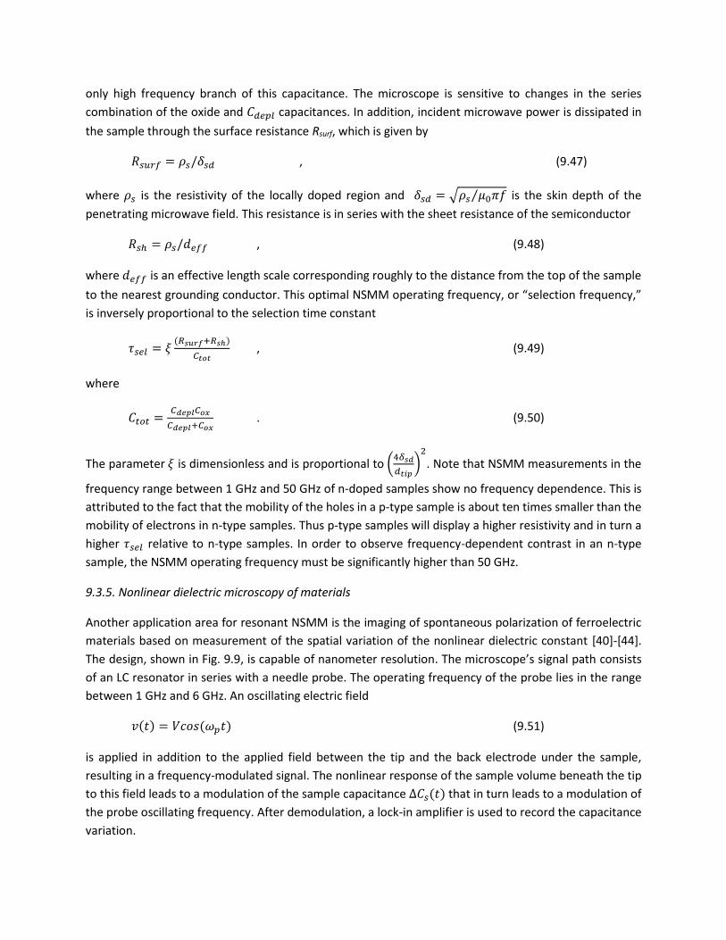
system in a Re(Y) vs. Im(Y) coordinate system, as is commonly done for spreading resistance data [52].
This representation is similar to well-known Cole-Cole diagrams that consist of a semicircle with the center
on the imaginary axis (for admittance). An example is shown in the left panel of Fig. 9.11. The radius of
the semicircle is
𝑟𝑠𝑐 =𝐶𝑐𝑝𝑙
2𝜔(1+𝐶𝑜𝑥 𝐶𝑐𝑝𝑙)⁄ (9.56)
and the angular distance
𝜑 = 2arctan (𝜔(𝐶𝑐𝑝𝑙 + 𝐶𝑜𝑥)𝑅𝑠) (9.57)
where 𝐶𝑜𝑥is the capacitance of the oxide layer and 𝐶𝑐𝑝𝑙 is the tip-sample coupling capacitance. For
comparison, a visualization of the complex admittance in the complex reflection coefficient plane is shown
in the right panel of Fig. 9.11. The reflection coefficient plane representation is a conformal mapping of
the admittance plane representation.
Figure 9.11 Visualization of the complex admittance. (Left panel) Y-plane spreading resistance plot. The
dots represent a series of logarithmically-scaled spreading resistances. (Right panel) The corresponding
spreading resistances plotted in the complex reflection coefficient (Γ) plane. [52] © IOP Publishing.
Reprinted with permission. All rights reserved.
Many early NSMM measurements of low-dimensional materials focused on graphene and an abundance
of work has been done to develop corresponding sample models. The relationship between the spreading
resistance 𝑅𝑠 of the graphene and the graphene sheet resistance 𝑅∎is given by [52]
𝑅𝑠 =𝑅∎
2𝜋𝑙𝑛
𝑟𝑔
𝑟𝑡 , (9.58)

where 𝑟𝑔 is the inner radius of the ground electrode and 𝑟𝑡 is the radius of the contact area to the
graphene sample. In the experimental configuration describe in Reference [52], 𝑟𝑔 is usually large and the
exact shape of the graphene patch does not significantly influence the result of Equation (9.58).
Investigation of the sheet resistance of graphene layers with different thicknesses led to a simplified
resistive model tied to the measurement of the reflection coefficient [53]. An alternative characterization
method measures the microwave conductivity of graphene by use of a high-Q resonator [54]. Like many
implementations of NSSM, the resonator method measures the shifts in the resonant frequency and the
quality factor, therefore the analysis is also applicable to NSMM measurements. First, resonator
measurements are made on both the bare substrate and the substrate with graphene layer. The change
of the resonator loss due to presence of the graphene can be obtained by taking the difference of the
measured quality factors. In turn, this difference can be related to the shift of the resonance frequency
due to presence of graphene sheet, the material dimensions and material properties. Application of
Equation (9.34) results in [54]
∆ (1
𝑄) = ∆ (
1
𝑄𝑔) − ∆ (
1
𝑄𝑠) = 휀𝑔
′′ ∆𝑓𝑠𝑡𝑔
( 𝑠′−1)𝑡𝑠
, (9.59)
where 𝑡𝑔 is the thickness of the graphene layer and 𝑡𝑠 is the thickness of the substrate. Similar notation
distinguishes the permittivity of the graphene εg from that of the substrate εs. The sheet resistance is
related to graphene conductivity by
𝑅𝑠 =1
𝜎𝑡𝑔 . (9.60)
Given the dependence between the conductivity and imaginary component of the dielectric constant,
𝜎 = 2𝜋𝑓0휀0휀𝑔′′, the sheet resistance is [54]
𝑅𝑠 =∆𝑓𝑠
2𝜋𝑓0 0∆(1
𝑄)( 𝑠
′−1)𝑡𝑠
. (9.61)
Returning to the particular case of NSMM, it is useful to introduce a simple model of the impedance of a
graphene sheet as well as other, similar two-dimensional materials. In one example [55], the tip-graphene
interaction in a NSMM was described by a lumped element model consisting of series connection of oxide
capacitance, spreading resistance of graphene, and the capacitance between the substrate and the shield
of the probe. Here, we develop a general approach based on a two dimensional electron gas (2DEG)
[56],[57]. The 2DEG impedance can be expressed as [57]
𝑍2𝐷𝐸𝐺 = 𝑅2𝐷𝐸𝐺 + 𝑗𝜔𝐿𝑘; 𝑅2𝐷𝐸𝐺 =𝑚𝑒𝑓𝑓
𝑁𝑒2𝜈; 𝐿𝑘 =
𝑚𝑒𝑓𝑓
𝑁𝑒2 (9.62)
where 𝑅2𝐷𝐸𝐺is the 2DEG resistance per square and 𝐿𝑘is the kinetic inductance. More generally, the
impedance for a sample of any thickness is determined by use of the Drude conductivity as [56]
𝑍𝑔𝑟 =𝑔𝐹+2𝑎
𝑁
1+𝑗𝜔𝜏
𝜎 (9.63)

where 𝑔𝐹 and a are form factors depending on the geometry of the probe, N is number of layers in the
graphene stack, 𝜏 is scattering time and 𝜎 = 𝜇𝑛𝑑𝑒 is the low frequency Drude two-dimensional
conductivity.
In order to develop a general model there is an additional parameter that has to be considered, namely
the quantum capacitance. Quantum capacitance was introduced in Reference [58] in connection with
two-dimensional electron gases and discussed in Reference [59] as an approach for modeling one-
dimensional nanoscale devices. The quantum capacitance is defined as
𝐶𝑄 =𝜕𝑄
𝜕𝑉𝑙 , (9.64)
where 𝑉𝑙 is a local electrostatic potential. The quantum capacitance is conventionally defined per unit
length for one-dimensional systems and per unit area for two-dimensional systems. The quantum
capacitance depends critically on the form of the density of states. Below we give a few examples of the
density of states and corresponding quantum capacitances.
In general, the density of states (DOS) is given by
𝑔(𝐸) =𝑚𝑒𝑓𝑓
𝜋ℏ2 𝜈(𝐸) , (9.65)
where 𝜈(𝐸) is the number of contributing bands at a given energy. Assuming that 𝜈(𝐸) may be
approximated by a quadratic dependence on energy E, the quantum capacitance for a two-dimensional
system is [59]
𝐶𝑄 =𝜈𝑚𝑒𝑓𝑓𝑒2
2𝜋ℏ2 [2 −sinh (𝐸𝐺 2𝑘𝑇⁄ )
𝑐𝑜𝑠ℎ(𝐸𝐺 2⁄ −𝑒𝑉𝑙
2𝑘𝑇)𝑐𝑜𝑠ℎ(
𝐸𝐺 2⁄ +𝑒𝑉𝑙2𝑘𝑇
)] (9.66)
where EG is the band gap. For EG =0 this reduces to [58]
𝐶𝑄 =𝜈𝑚𝑒𝑓𝑓𝑒2
2𝜋ℏ2 (9.67)
Alternatively, for undoped, single-layer graphene, a linear density of states may be used. If the density
of states has the form [60, 61]
𝑔(𝐸) =𝑔𝑠𝑔𝑣
2𝜋(ℏ𝑣𝐹)2 |𝐸| (9.68)
where 𝑔𝑠 is the spin degeneration and 𝑔𝑣 is the valley parameter, then the quantum capacitance is
given by
𝐶𝑄 =2𝑒2𝑘𝑇
𝜋(ℏ𝑣𝐹)2 ln [2 (1 + cosh (𝑒𝑉𝑙
𝑘𝑇))] , (9.69)
where k is the Boltzman constant. Under the condition 𝑒𝑉𝑙 ≫ 𝑘𝑇, Equation (9.69) simplifies to
𝐶𝑄 ≈ 𝑒2 2𝑒𝑉𝑙
𝜋(ℏ𝑣𝐹)2 =2𝑒2
ℏ𝑣𝐹√𝜋√𝑛 , (9.70)
where n is the carrier concentration and e is the electron charge.
In the one-dimensional case
𝑔(𝐸) =1
𝜋ℏ2 𝜈(𝐸)√2𝑚𝑒𝑓𝑓
𝐸 (9.71)
and the calculation of the quantum capacitance is more complicated. Under special conditions, if 𝜈 can
be considered constant and the DOS can be approximated as
𝑔(𝐸) =𝜈
ℎ𝑣𝐹 , (9.72)
where 𝑣𝐹 is the Fermi velocity, then the one-dimensional quantum capacitance simplifies to
𝐶𝑄 =2𝜈𝑒2
ℎ𝑣𝐹 . (9. 73)
Experimentally, the local quantum capacitance of graphene or other low dimensional system can be
obtained by use of scanning probe microscopy and spectroscopy [62]. Although such measurements have
historically been performed with scanning capacitance microscopes, they can also be performed with
NSMM. The NSMM tip is positioned near the sample and the reflection coefficient is measured as a
function of the tip bias voltage. As needed, a small AC signal may be added to the DC bias to facilitate a
more sensitive spectroscopic measurement by use of a lock-in technique.
Consider such a spectroscopic measurement of a mechanically exfoliated graphene flake supported by a
SiO2 layer grown on a Si substrate. Spectroscopic measurements are taken at tip positions above the
graphene flake as well as above the bare SiO2. The ratio of the reflection coefficient measured with the
tip positioned over the graphene to that measured with the tip positioned over the oxide is calculated.
Once again, the system consisting of the probe tip over the oxide and Si substrate can be reasonably
modeled as a MOS structure, but the model must be modified such that the quantum capacitance is in
series with the MOS impedance. The quantum capacitance per unit area CQ may then be related to the
oxide capacitance per unit area Cox by
𝐶𝑄 = 𝐶𝑜𝑥𝑉𝑏
∆𝑉𝑔𝑟 (9.74)
where 𝑉𝑏 is the bias voltage and ∆𝑉𝑔𝑟 is the potential drop across the thickness of the graphene within
the effective probe area. The local potential in graphene is dependent on the charge density around the
contact and can be expressed as [62]
𝑉𝑔𝑟(𝑟) =√𝜋ℏ𝑣𝐹
𝑒√|𝑛(𝑟)| . (9.75)
The potential drop within the effective probe area is then obtained by integrating the potential over the
effective tip area. The charge density distribution n(r) depends on the geometry and structure of the
measured system and must be calculated either numerically or analytically.

9.4.4. Measurements of transition metal dichalcogenides
Let’s turn now from the case of exfoliated graphene to the case of two-dimensional semiconductors,
including transition metal dichalcogenides (TMDs). Electrical properties of several TMDs, including
metallic and semiconducting systems, are shown in Table 1 [63]. Other two-dimensional semiconductor
materials include silicine, phosphorene, and hexagonal boron nitride. Unlike graphene, semiconducting
TMDs have a bandgap and are thus suitable for transistor applications.
Table 9.1. Properties of transition metal dichalcogenides. Single-layer (1L) and bulk band gaps are listed
for the semiconducting materials. Reprinted by permission from Macmillan Publishers Ltd: Nature
Nanotechnology. Q. Hua Wang, K. Kalantar-Zadeh, A. Kis, J. N. Coleman and M. S. Strano, Nature
Nanotechnology 7 (2012) pp. 699-712. Copyright 2012.
-S2 -Se2 -Te2
Electronic
Characteristics
Ref. Electronic
Characteristics
Ref. Electronic
Characteristics
Ref.
Nb Metal;
Superconductor;
Charge Density
Wave
[67] Metal;
Superconductor;
Charge Density
Wave
[67],[68] Metal [72]
Ta Metal;
Superconducting;
Charge Density
Wave
[67],[68] Metal;
Superconducting;
Charge Density
Wave
[67],[68] Metal [72]
Mo Semiconductor
1L: 1.8 eV
Bulk: 1.2 eV
[69],[70] Semiconductor
1L: 1.5 eV
Bulk: 1.1 eV
[71],[70] Semiconductor
1L: 1.1 eV
Bulk: 1.0 eV
[71],[73]
W Semiconductor
1L: 1.9 eV - 2.1
eV
Bulk: 1.2 eV
[66],[71],
[70]
Semiconductor
1L: 1.7 eV
Bulk: 1.2 eV
[72],[70] Semiconductor
1L: 1.1 eV
[72]
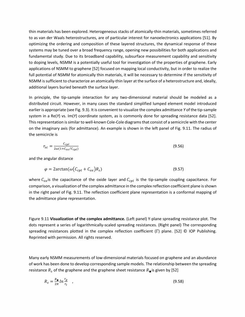
Representative TMD materials MoS2 and WSe2 have been investigated by NSMM [64], revealing that the
sensitivity of NSMM is sufficient to image monolayer semiconducting materials and perform quantitative
spectroscopy on them. The signal-to-noise ratio was found to be dependent on the polarity of the tip bias.
Fig. 9.12(a) shows NSMM images of a mechanically exfoliated, few-layer W1-x NbxSe2 patch on a SiO2/Si
substrate while Fig. 9.12(b) shows NSMM images of a single layer MoS2. To acquire these images a lock-
in technique was used to obtain the real and imaginary parts of the derivative of the reflection coefficient
(SR’ = Re(dS11/dVtip), SC’ = Im(dS11/dVtip)). The images demonstrate that changes in the DC tip bias induce
different levels of contrast in the SR’ image. Further investigation revealed that for a given material,
contrast was observed for only one polarity of the tip bias, which was directly correlated with the polarity
of the charge carriers in the material. There is little contrast in the SC’ images, regardless of tip bias polarity
or magnitude.
Figure 9.12. NSMM images of transition metal dichalcogenides. AFM topography (i) and NSMM images
(ii-v) of (a) an exfoliated few-layer W1-x NbxSe2 sample; (b) and a single layer MoS2 sample with tip bias as
indicated. Reprinted with permission from S. Berweger, et. al., Nano Letters 15 (2015) pp. 1122-1127.
Copyright 2015, American Chemical Society.
Further insight into the interpretation of the NSMM measurements was gained through finite-element,
multiphysics simulation of the NSMM-TMD system. The objective of the simulation process is to connect
the simulated parameters with the materials properties of the sample by relating them to the measured,
bias-dependent data. While this approach is phenomenological, it provides insight into the underlying
physics with the NSMM probe-TMD sample system. In this case, it is useful to understand the relation
between the charge carrier density and the bias voltage Vtip. Specifically, the real part of the measured
admittance of the TMD materials was modeled as a function of conductivity. The capacitive behavior of
the TMDs was captured by modeling the material as a dielectric sheet with the relative permittivity r =7.
If the band edge DOS is approximated by a quadratic function, the relation between the carrier density nq
and the conductivity of the given material can be expressed as [65],[66]
𝑛𝑞 ∝ ∓(𝑎𝑉𝑡𝑖𝑝 − 𝐸0)3
= 𝜎𝑖 (9. 76)
where the minus sign corresponds to n-type semiconductor (as in MoS2) and the plus sign to the p-doped
semiconductor (as in WSe2). The constant a reflects the scaling between E and Vtip and E0 accounts for
doping at zero bias i.e., the Fermi level shift. It is important to note that a reasonable guess from existing
published data or independent measurements must be used to make a reasonable estimate of the
mobility of the carriers, as this parameter also enters the relation between the charge carriers and the
conductivity of the material. Based on the comparison of the model with the experimental data, the tip-
bias dependent contrast is attributed to changes of the TMD conductivity. Measurements and modeling
agree that both MoS2 and WSe2 show strong unipolar charge transport that correlates with the polarity-
dependent contrast in NSMM images.
In addition to NSMM imaging, local spectroscopy can be performed at any tip position above the
investigated sample. Of especial importance is spectroscopy on single-layer regions, which provides local
measurements of electronic structure as well as sensitivity to local defects. Examples of local
spectroscopic measurements of TMD samples are shown in Fig. 9.13. The predicted spectra of the
phenomenological, numerical modeling are in good agreement with the experimental data. In order to fit
the capacitive part of the spectra, it was necessary to include the quantum capacitance in series with the
geometric, electrostatic capacitance. Interpretation of NSMM measurements of semiconducting, two-
dimensional materials is more challenging than the interpretation of NSMM measurements of graphene,
requiring not only consideration of the effects of quantum capacitance, but also accurate modeling of the
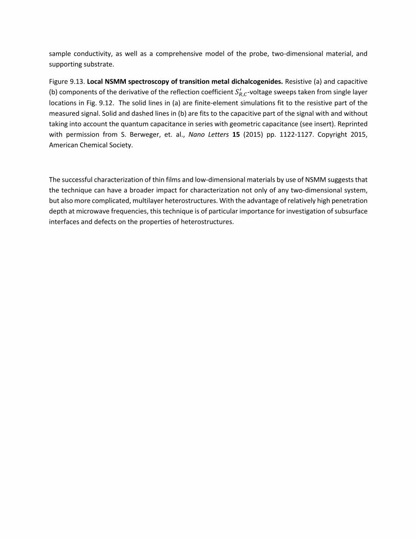
sample conductivity, as well as a comprehensive model of the probe, two-dimensional material, and
supporting substrate.
Figure 9.13. Local NSMM spectroscopy of transition metal dichalcogenides. Resistive (a) and capacitive
(b) components of the derivative of the reflection coefficient 𝑆𝑅,𝐶′ -voltage sweeps taken from single layer
locations in Fig. 9.12. The solid lines in (a) are finite-element simulations fit to the resistive part of the
measured signal. Solid and dashed lines in (b) are fits to the capacitive part of the signal with and without
taking into account the quantum capacitance in series with geometric capacitance (see insert). Reprinted
with permission from S. Berweger, et. al., Nano Letters 15 (2015) pp. 1122-1127. Copyright 2015,
American Chemical Society.
The successful characterization of thin films and low-dimensional materials by use of NSMM suggests that
the technique can have a broader impact for characterization not only of any two-dimensional system,
but also more complicated, multilayer heterostructures. With the advantage of relatively high penetration
depth at microwave frequencies, this technique is of particular importance for investigation of subsurface
interfaces and defects on the properties of heterostructures.
References
[1] S. R. de Groot and L. G. Suttorp, Foundations of electrodynamics (American Elsevier, 1972).
[2] U. Kaatze, “Techniques for measuring the microwave dielectric properties of materials,” Metrologia 47 (2010)
pp. S91-S113.
[3] L. D. Landau and E. M. Lifshitz, Electromagnetic of Continuous Media (Addison-Wesley, 1960).
[4] J. D. Jackson, Classical Electrodynamics, 3rd Ed. (Wiley, 1999).
[5] R. Hornreich and S. Shtrikman, Physical Review 161 (1967) pp. 506-512.
[6] G. T. Rado, Physical Review 128 (1962) pp. 2546-2556.
[7] J. Baker-Jarvis and P. Kabos, “Dynamic constitutive relations for polarization and magnetization,” Physical
Review E 64 (2001) art. no. 056127.
[8] J. Baker-Jarvis, P. Kabos, and C. Holloway, “Nonequilibrium electromagnetics: Local and macroscopic fields and
constitutive relationships,” Physical Review E 70 (2004) art. no. 036615.
[9] S. M. Anlage, V. V. Talanov, and A. R. Schwartz, “Principles of near field microscopy,” in Scanning Probe
Microscopy, vol. 1, S. Kalinin and A. Gruverman, eds. (Springer, 2007).
[10] A. N. Reznik and N. V. Yurasova, “Electrodynamics of microwave near field probing: Application to medical
diagnostics,” Journal of Applied Physics 98 (2005) art. no. 114701.
[11] S.-C Lee, C. P. Vlahacos, B. J. Feenstra, A. Schwartz, D. E. Steinhauer, F. C. Wellstood, and S. M. Anlage,
“Magnetic permeability imaging of metals with scanning near-field microwave microscope,” Applied Physics Letters
77 (2000) pp. 4404-4406.
[12] A. N. Reznik, “Electromagnetic model for near field microwave microscope with atomic resolution:
Determination of tunnel junction impedance,” Applied Physics Letters 105 (2014) art. no. 083512.
[13] A. Hovsepyan, A. Babajanyan, T. Sargsyan, H. Melikyan, S. Kim, J. Kim, K Lee and B. Friedman, “Direct imaging
of photoconductivity of solar cells by using near-field scanning microwave probe,” Journal of Applied Physics 106
(2009) art. no. 114901.
[14] J. R. Wait, Electromagnetic waves in stratified media, (Pergamon Press, 1962).
[15] J. R. Wait, Wave propagation theory, (Pergamon Press, 1981).
[16] W. Ch. Chew, Waves and fields in inhomogeneous media, (Van Nostrand Reinhold, 1990).
[17] C. Gao and X.-D. Xiang, “Quantitative microwave near field microscopy of dielectric properties,” Review of
Scientific Instruments 69 (1998) pp. 3846-3851.
[18] G. P. Kochanski, “Nonlinear alternating-current tunneling microscopy.” Physical Review Letters 62 (1989)
pp.2285-2288.
[19] M. Tabib-Azar, D. -P. Su, A. Pohar, S. R. LeClair, G. Pochak, “0.4 m spatial resolution with 1 GHz (=30cm)
evanescent microwave probe,” Review of Scientific Instruments 70 (1999) pp. 1725-1729.
[20] M. Tabib-Azar and S. R. LeClair, “Novel hydrogen sensors using evanescent microwave probes,” Review of Scientific Instruments 70 (1999) pp. 3707–3713. [21] R. A. Kleinsmit, M. K. Kazimierczuk and G. Kozlowski, “Sensitivity and resolution of evanescent microwave
microscope,“ IEEE Transactions on Microwave Theory and Techniques 54 (2006) pp. 639-647.
[22] S. J. Stranick and P. S. Weiss, “A versatile microwave-frequency-compatible scanning tunneling microscope,”
Review of Scientific Instruments 64 (1993) pp. 1232-1234.
[23] Y. Cho, “Scanning nonlinear dielectric microscope with super high resolution,” Japanese Journal of Applied
Physics 46 (2007) pp. 4428-4434.
[24] J. Smoliner, H. P. Huber, M. Hochleitner, M. Moertelmaier, and F. Kienberger, “Scanning microwave
microscopy/spectroscopy on metal oxide semiconductor systems,” Journal of Applied Physics 108 (2010) art. no.
064315.
[25] D. A. Hill, Electromagnetic field in cavities, IEEE Press Series on Electromagnetic wave theory, (John Willey
&Sons, 2009).
[26] A. Tselev, S. M. Anlage, Z. Ma and J. Melngailis, “Broadband dielectric microwave microscopy on micron length
scales,” Review of Scientific Instruments 78 (2007) art. no. 044701.
[27] D. M. Pozar, Microwave Engineering, 2nd ed., (Willey, 1998).
[28] K. D. McKinstry and C. E. Patton, “ Methods for determination of microwave cavity quality factors from
equivalent circuit models,” Review of Scientific Instruments 60 (1989) pp. 439-443.
[29] A. Imtiaz, T. Baldwin, H. T. Nembach, T. M. Wallis and P. Kabos, “Near field microscope measurements to
characterize bulk material properties,” Applied Physics Letters 90 (2007) art. no. 243105.
[30] D. J. Barker, T. J. Jackson, P. M. Suherman, M. S. Gashinova, and M. J. Lancaster, “Uncertainties in the
permittivity of think films extracted from the measurements with near field microwave microscopy calibrated by
image charge model,“ Measurement Science and Technology 25 (2014) art. no. 105601.
[31] R. A. Oliver, “Advances in AFM for the electrical characterization of semiconductors,” Rep. Prog. Phys. 71
(2008) art. no. 076501.
[32] H. P. Huber, I. Humer, M. Hochleitner, M. Fenner, M. Moertelmaier, C. Rankl, A. Imtiaz, T. M. Wallis, H. Tanbakuchi, P. Hinterdorfer, P. Kabos, J. Smoliner, J. J. Kopanski, and F. Kienberger, “Calibrated nanoscale dopant profiling using scanning microwave microscope,” Journal of Applied Physics 111 (2012) art. no. 014301. [33] S. M. Sze, The Physics of Semiconductor Devices, (Wiley, 1981).
[34] J. J. Kopanski, J. F. Marchiando, and J. R. Lowney, “Scanning capacitance microscopy applied to two-
dimensional dopant profiling of semiconductors,” Mater. Sci. Eng. B-Solid State Mater. Adv. Tech. 44 (1997) pp. 46-
51.
[35] J. F. Marchiando, J. J. Kopanski, and J. R. Lowney, “Model database for determining dopant profiles from
scanning capacitance microscope measurements,” Journal of Vacuum Science and Technology B 16 (1998) pp. 463-
470.
[36] J. Smoliner, B. Basnar, S. Golka, E. Gornik, B. Lo¨ffler, M. Schatzmayr, and H. Enichlmair, “Mechanism of bias-
dependent contrast in scanning-capacitance microscopy images,” Applied Physics Letters 79 (2001) pp. 3182-3184.
[37] A. Imtiaz, S. M. Anlage, J. D. Barry and J. Melngailis, “Nanometer-scale material contrast imaging with a near-
field microwave microscope,” Applied Physics Letters 90 (2007) art. no. 143106.
[38] A. Imtiaz, T. M. Wallis, S.-H. Lim, H. Tanbakuchi, H.-P. Huber, A. Hornung, P. Hinterdorfer, J. Smoliner, F.
Kienberger, and P. Kabos, “Frequency selective contrast on variable doped p-type silicon with a scanning
microwave microscope,” Journal of Applied Physics 111 (2012) art. no. 093727.
[39] E. H. Nicollian and J. R. Brews, MOS (Metal Oxide Semiconductor) Physics and Technology (Wiley, 1982).
[40] Y. Cho, A. Kirihara, T. Saeki, “Scanning nonlinear dielectric microscope,” Review of Scientific Instruments 67
(1996) pp.2297-2303.
[41] Y. Cho, S. Kazuta, and K. Matsuura, “Scanning nonlinear dielectric microscopy with nanometer resolution,”
Applied Physics Letters 75 (1999) pp.2833-2835.
[42] R. Hirose, K. Ohara, and Y. Cho, “Observation of the Si(111) 7x7 atomic structure using noncontact scanning
nonlinear dielectric microscopy,” Nanotechnology 18 (2007) art. no. 084014.
[43] K. Tanaka, Y. Kurihashi, T. Uda, Y. Daimon, N. Odagawa, R. Hirose, Y. Hiranaga, and Y. Cho, “Scanning nonlinear
dielectric microscopy nanp-science and technology for next generation high density ferroelectric data storage,”
Japanese Journal of Applied Physics 47 (2008) pp. 3311-3325.
[44] Y. Cho, “Scanning nonlinear dielectric microscopy,” Journal of Materials Research 26 (2011) pp.2007-2016.
[45] D. A. Bonnel, D. N. Basov, M. Bode, U. Diebold, S. V. Kalinin. V. Madhavan, L. Novotny, M. Salmeron, U. D.
Schwartz, P. S. Weiss, “Imaging physical phenomena with local probes: From electrons to photons,” Reviews of
Modern Physics 84 (2012) pp.1343-1381.
[46] J. Baker-Jarvis and S. Kim, “The Interaction of Radio-Frequency Fields With Dielectric Materials at Macroscopic to Mesoscopic Scales,” Journal of Research of the National Institute of Standards and Technology 117
(2012) pp. 1-60.
[47] P. Qu´eff´elec, M. Le Floc’h, and P. Gelin, “Broad-Band Characterization of Magnetic and Dielectric Thin Films
Using a Microstrip Line,” IEEE Transactions on Instrumentation and Measurement 47 (1998) pp.956-963.
[48] S. Huang, H. M. Christen, and M. E. Reeves, “Parameter-free extraction of Thin-Film Dielectric Constants from
Scanning Near Field Microwave Microscope Measurements,” arXiv:00909.3579v1 [cond-mat.sci] (2009).
[49] J. H. Lee, S. Hyun, and K. Char, “Quantitative analysis of scanning microwave microscopy on dielectric thin film by finite element calculation,” Review of Scientific Instruments 72 (2001) pp. 1425-1434. [50] G. Fiori, F. Bonaccorso, G. Iannaccone, T. Palacios, D. Neumaier, A. Seabaugh, S. K. Banerjee and L. Colombo,” Electronics based on two-dimensional materials,” Nature Nanotechnology 9 (2014) pp.768-779.

[51] A. K. Geim and I. V. Grigorieva, “Van der Waals heterostructures,” Nature 499 (2013) pp. 419-425. [52] A. Tselev, N. V. Lavrik, I. Vlassiouk, D. P. Briggs, M. Rutgers, R. Proksch and S. V. Kalinin,” Near-field microwave scanning probe imaging of conductivity inhomogeneities in CVD graphene,” Nanotechnology 23 (2012) art. no. 385706. [53] T. Monti, A. Di Donato, D. Mencarelli, G. Venanzoni, A. Morini, and M. Farina, “Near-Field Microwave Investigation of Electrical Properties of Graphene-ITO Electrodes for LED Applications,” Journal of Display Technology 9 (2013) pp.504-510. [54] L. Hao, J. Gallop, S. Goniszewski, O. Shaforost, N. Klein, and R. Yakimova, “Non-contact method for measurement of microwave conductivity of graphene,” Applied Physics Letters 103 (2013) art. no. 123103. [55] A. Tselev, V. K. Sangwan, D. Jariwala, T. Marks, L. J. Lauhon, M. C. Hersam, and S. V. Kalinin, “Near field
microwave microscopy of high-k oxides grown on graphene with an organic seed layer,” Applied Physics Letters
103 (2013) art. no. 243105.
[56] V. V. Talanov, C. Del Barga, L. Wickey, I. Kalichava, E. Gonzales, E. A. Shaner, A. V. Gin, and N. G. Kalugin, “Few-
Layer Graphene Characterization by Near-Field Scanning Microwave Microscopy,” ACS Nano 4 (2010) pp. 3831–
3838.
[57] Kang, S.; Burke, P. J.; Pfeiffer, L. N.; West, K. W. AC Ballistic, “Transport in a Two-Dimensional Electron Gas
Measured in GaAs/AlGaAs Heterostructures.” Physical Review B 72 (2005) art. no. 165312.
[58] S. Luryi, “Quantum capacitance devices,” Applied Physics Letters 52 (1988) pp. 501-503.
[59] D. L. John, L. C. Castro, and D. L. Pulfrey, “Quantum capacitance in nanoscale device modeling,” Journal of
Applied Physics 96 (2004) pp. 5180-5184.
[60] T. Fang, A. Konar, H. Xing, and D. Jena, “Carrier statistics and quantum capacitance of graphene sheets and
ribbons,” Applied Physics Letters 91 (2007) art. no. 092109.
[61] J. Xia, F. Chen, J. Li and N. Tao, “Measurement of the quantum capacitance of graphene,” Nature
Nanotechnology 4 (2009) pp.505-509.
[62] F. Giannazzo, S. Sonde, V. Raineri, and E. Rimini, “Screening Length and Quantum Capacitance in Graphene by
Scanning Probe Microscopy,” Nano Letters 9 (2009) pp.23-29.
[63] Q. Hua Wang, K. Kalantar-Zadeh, A. Kis, J. N. Coleman and M. S. Strano, “Electronics and optoelectronics of
two-dimensional transition metal dichalcogenides,” Nature Nanotechnology 7 (2012) pp. 699-712.
[64] S. Berweger, J. C. Weber, J. John, J. M. Velazquez, A. Pieterick, N. A. Sanford, A. V. Davydov, B. Brunschwig, N.
S. Lewis, T. M. Wallis, and P. Kabos,” Microwave Near-Field Imaging of Two-Dimensional Semiconductors,” Nano
Letters 15 (2015) pp. 1122-1127.
[65] E. S. Kadantsev and P. Hawrylak, “Electronic structure of single MoS2 monolayer” Solid State Communications
152 (2012) pp. 909-913.
[66] A. Kuc, N. Zibouche, and T. Heine, “Influence of quantum confinement on the electronic structure of the
transition metal sulfide TS2” Physical Review B 83 (2011) art. no. 245213.

[67] A. R. Beal, H. P. Hughes, and W. Y. Liang, “The reflectivity spectra of some group VA transition metal
dichalcogenides” Journal of Physics C 8 (1975) pp. 4236-4248.
[68] J. A. Wilson, F. J. Di Salvo, and S. Mahajan, “Charge-density waves and superlattices in the metallic layered
transition metal dichalcogenides,” Advances in Physics. 24 (1975) pp. 117–201.
[69] K. F. Mak, C. Lee, J. Hone, J. Shan, and T. F. Heinz, “Atomically thin MoS2: a new direct-gap semiconductor,”
Physical Review Letters 105 (2010) art. no. 136805.
[70] K. K. Kam and B. A. Parkinson, “Detailed photocurrent spectroscopy of the semiconducting group-VI transition-
metal dichalcogenides,” Journal of Physical Chemistry 86 (1982) pp. 463–467.
[71] L. Liu, S. B. Kumar, Y. Ouyang, and J. Guo, “Performance limits of monolayer transition metal dichalcogenide
transistors,” IEEE Transactions on Electron Devices 58 (2011) pp. 3042–3047.
[72] Y. Ding, Y. Wang, J. Ni, L. Shi, S. Shi, and W. Tang, “First principles study of structural, vibrational and electronic
properties of graphene-like MX2 (M=Mo, Nb, W, Ta; X=S, Se, Te) monolayers,” Physica B: Condensed Matter 406
(2011) pp. 2254–2260.
[73] Gmelin Handbook of Inorganic and Organometallic Chemistry 8th ed. Vol. B7 (Springer, 1995).
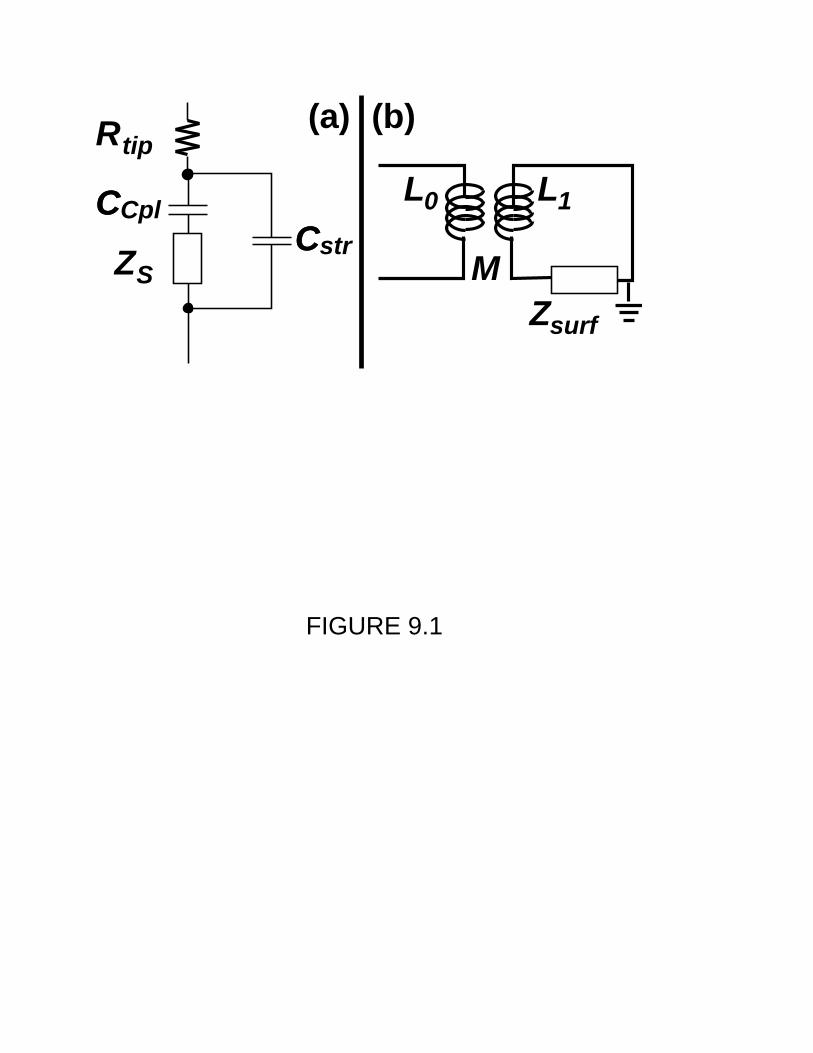
(a)
CCstr
CCCpl
Rtip
ZS
FIGURE 9.1
(b)
L0 L1
Zsurf
M


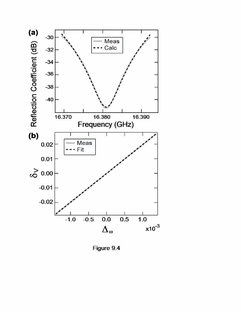

Figure 9.5

Figure 9.6
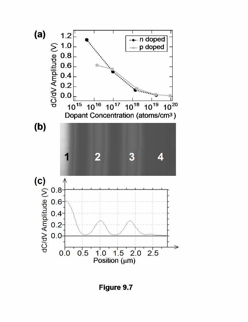


Figure 9.9

5 nm
Figure 9.10
Figure 9.11

Figure 9.12
Figure 9.13


