
Combinational Circuits (DC-IV) MCQs &
Numerical Problems
The problems considered here are put under the following five subtopics. These are:
(a) Arithmetic circuits
(b) Multiplexers
(c) Decoders and encoders
(d) Code converters
(e) Comparators
Some problems have been taken from previous GATE examination and some other problems are
added for practice.
Special efforts are put to arrange them in the increasing order of their complexity, so that it is
easier to learn progressively.
Video solution to some typical Gate problems will be given separately.
Arithmetic Circuits
1. For a binary half adder having two inputs A and B the correct set of logical expressions
the output
𝑆(= 𝐴 𝑝𝑙𝑢𝑠 𝐵) 𝑎𝑛𝑑 𝐶(= 𝑐𝑎𝑟𝑟𝑦)
Are: (also given logic diagram)
(a) 𝑆 = 𝐴𝐵 + �̅�𝐵 & 𝐶 = �̅�𝐵
(b) 𝑆 = �̅�𝐵 + 𝐴�̅� & 𝐶 = 𝐴𝐵
(c) 𝑆 = �̅�𝐵 + 𝐴�̅� & 𝐶 = �̅�𝐵
(d) 𝑆 = 𝐴𝐵 + �̅��̅� & 𝐶 = 𝐴�̅�
Sol. Half adder: logic circuit which adds two one bit number is called half adder.
Truth table
Inputs
A B
Outputs
S (sum) C
(carry)
0 0
0 1
1 0
1 1
0 0
1 0
1 0
0 1
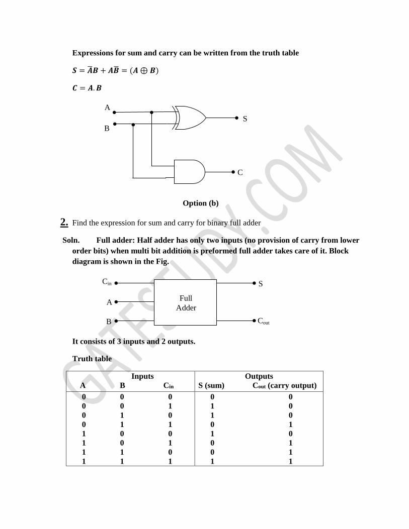
Expressions for sum and carry can be written from the truth table
𝑺 = �̅�𝑩 + 𝑨�̅� = (𝑨 ⊕ 𝑩)
𝑪 = 𝑨. 𝑩
A
B
C
S
Option (b)
2. Find the expression for sum and carry for binary full adder
Soln. Full adder: Half adder has only two inputs (no provision of carry from lower
order bits) when multi bit addition is preformed full adder takes care of it. Block
diagram is shown in the Fig.
Full
Adder
Cin
A
B
S
Cout
It consists of 3 inputs and 2 outputs.
Truth table
Inputs
A B Cin
Outputs
S (sum) Cout (carry output)
0 0 0
0 0 1
0 1 0
0 1 1
1 0 0
1 0 1
1 1 0
1 1 1
0 0
1 0
1 0
0 1
1 0
0 1
0 1
1 1

𝑺 = �̅��̅� 𝑪𝒊𝒏 + �̅�𝑩�̅�𝒊𝒏 + 𝑨�̅��̅�𝒊𝒏 + 𝑨𝑩𝑪𝒊𝒏
= �̅�(�̅�𝑪𝒊𝒏 + 𝑩�̅�𝒊𝒏) + 𝑨(�̅��̅�𝒊𝒏 + 𝑩𝑪𝒊𝒏)
𝑺 = �̅�(𝑩 ⊕ 𝑪𝒊𝒏) + 𝑨(𝑩 ⊕ 𝑪𝒊𝒏̅̅ ̅̅ ̅̅ ̅̅ ̅̅ ̅)
𝑺 = 𝑨 ⊕ 𝑩 ⊕ 𝑪𝒊𝒏 (1)
𝑪𝒐𝒖𝒕 = �̅�𝑩𝑪𝒊𝒏 + 𝑨�̅�𝑪𝒊𝒏 + 𝑨𝑩�̅�𝒊𝒏 + 𝑨𝑩𝑪𝒊𝒏
= 𝑩𝑪𝒊𝒏(𝑨 + �̅�) + 𝑨�̅�𝑪𝒊𝒏 + 𝑨𝑩𝑪𝒊𝒏
𝑪𝒐𝒖𝒕 = 𝑩𝑪𝒊𝒏 + 𝑨�̅�𝑪𝒊𝒏 + 𝑨𝑩𝑪𝒊𝒏̅̅ ̅̅
This expression can be written in the following form
𝑪𝒐𝒖𝒕 = 𝑩𝑪𝒊𝒏 + 𝑨𝑪𝒊𝒏 + 𝑨𝑩 (2)
K-map simplification can also be done for above expressions full adder can also be
implemented using two half adders and one OR gate. Figure gives such
implementations
A
B S
Cin
Cout
The Soutput from the second half adder is EX-OR of Cin. Cout is as per the expression,
used modulo 2 adders instead of simple adder.
It is implemented with two half adders and one OR gate.
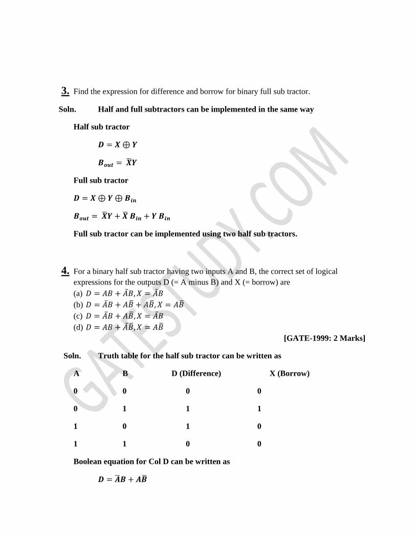
3. Find the expression for difference and borrow for binary full sub tractor.
Soln. Half and full subtractors can be implemented in the same way
Half sub tractor
𝑫 = 𝑿 ⊕ 𝒀
𝑩𝒐𝒖𝒕 = �̅�𝒀
Full sub tractor
𝑫 = 𝑿 ⊕ 𝒀 ⊕ 𝑩𝒊𝒏
𝑩𝒐𝒖𝒕 = �̅�𝒀 + �̅� 𝑩𝒊𝒏 + 𝒀 𝑩𝒊𝒏
Full sub tractor can be implemented using two half sub tractors.
4. For a binary half sub tractor having two inputs A and B, the correct set of logical
expressions for the outputs D (= A minus B) and X (= borrow) are
(a) 𝐷 = 𝐴𝐵 + �̅�𝐵, 𝑋 = �̅�𝐵
(b) 𝐷 = �̅�𝐵 + 𝐴�̅� + 𝐴�̅�, 𝑋 = 𝐴�̅�
(c) 𝐷 = �̅�𝐵 + 𝐴�̅�, 𝑋 = �̅�𝐵
(d) 𝐷 = 𝐴𝐵 + �̅��̅�, 𝑋 = 𝐴�̅�
[GATE-1999: 2 Marks]
Soln. Truth table for the half sub tractor can be written as
A B D (Difference) X (Borrow)
0 0 0 0
0 1 1 1
1 0 1 0
1 1 0 0
Boolean equation for Col D can be written as
𝑫 = �̅�𝑩 + 𝑨�̅�
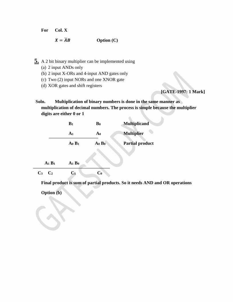
For Col. X
𝑿 = �̅�𝑩 Option (C)
5. A 2 bit binary multiplier can be implemented using
(a) 2 input ANDs only
(b) 2 input X-ORs and 4-input AND gates only
(c) Two (2) input NORs and one XNOR gate
(d) XOR gates and shift registers
[GATE-1997: 1 Mark]
Soln. Multiplication of binary numbers is done in the same manner as
multiplication of decimal numbers. The process is simple because the multiplier
digits are either 0 or 1
B1 B0 Multiplicand
A1 A0 Multiplier
A0 B1 A0 B0 Partial product
A1 B1 A1 B0
C3 C2 C1 C0
Final product is sum of partial products. So it needs AND and OR operations
Option (b)

Multiplexers
6. The logic function implemented by the circuit below is (ground implies a logic “0”)
P Q
F
4 x 1 MUX
S0S1
I0
I1
I2
I3
Y
(a) F = AND (P,Q)
(b) F = OR (P,Q)
(c) F = XNOR (P,Q)
(d) F = XOR (P,Q)
[GATE -2011: 1Mark]
Soln. Above circuit is redrawn to indicate the voltage levels
Truth table for MUX can be written as:
P Q F
0 0 0
0 1 1
1 0 1
1 1 0

P Q
F
4 x 1 MUX
S0S1
I0
I1
I2
I3
Y
0 1 0
1
1
0
Output F can be written as
𝑭 = �̅�𝑸 + 𝑷�̅� = 𝑷 ⊕ 𝑸
Option (d)
7. The Boolean function realized by the logic circuit shown is
A B
F(A,B,C,D)4 x 1
MUX
S0S1
I0
I1
I2
I3
C
D
(a) F = Ʃm (0,1,3,5,9,10.14)
(b) F = Ʃm (2,3,5,7,8,12.13)
(c) F = Ʃm (1,2,4,5,11,14.15)
(d) F = Ʃm (2,3,5,7,8,9.12)
[GATE-2010: 2 Marks]
Soln. Output can be written as
𝑭 = �̅��̅�𝑪 + �̅�𝑩𝑫 + 𝑨�̅��̅� + 𝑨𝑩(�̅�. �̅�)
Since the result is to be given in min term form, we expand the terms.
𝑭 = �̅��̅�𝑪(𝑫 + �̅�) + �̅�𝑩𝑫(𝑪 + �̅�) + 𝑨�̅��̅�(𝑫 + �̅�) + 𝑨𝑩�̅��̅�
Min. terms are put in K-map

00 01 11 10CD
AB
00
01
11
10
1
1
1
1 1
1
1
𝑭 = ∑ 𝒎 (𝟐, 𝟑, 𝟓, 𝟕, 𝟖, 𝟗, 𝟏𝟐)
Option (d)
8. What are the minimum number of 2-to-1 multiplexers required to generate a 2- input
AND gate and a 2-input Ex-OR gate?
(a) 1 and 2
(b) 1 and 3
(c) 1and 1
(d) 2 and 2
[GATE-2009: 2 Marks]
Soln. Consider 2-input AND gate
Let the variables are A and B
0
A
B
I0
I1
B is used in select line.
𝑭 = �̅�. 𝟎 + 𝑩. 𝑨 = 𝑨𝑩 AND gate
2-input EX-OR gate
Let the variables be A & B for EX-OR gate complements of variable are also needed
𝑭 = �̅�𝑨 + �̅�𝑩

1
0
A
A
A
B
Y
I0
I1
I0
A
Option (a) 1 and 2
9. For the circuit shown in the following figure, I0 – I3 are input to the 4:1 multiplexer R
(MSB) and S are control bits.
R S
Z4 x 1
MUX
I3
I2
I1
I0
P
P
Q
P
P
Q
The output Z can be represented by
(a) 𝑃𝑄 + 𝑃�̅�𝑆 + �̅��̅�𝑆̅
(b) 𝑃�̅� + 𝑃𝑄�̅� + �̅��̅�𝑆̅
(c) 𝑃�̅��̅� + �̅�𝑄𝑅 + 𝑃𝑄𝑅𝑆 + �̅��̅�𝑆̅
(d) 𝑃𝑄�̅� + 𝑃𝑄𝑅𝑆̅ + 𝑃�̅��̅�𝑆 + �̅��̅�𝑆̅
[GATE-2008: 2 Marks]
Soln. �̅��̅�. (𝑷 + �̅�) + �̅�𝑺. 𝑷 + 𝑹�̅�𝑷𝑸 + 𝑹𝑺𝑷
= �̅��̅�𝑷 + �̅��̅��̅� + �̅�𝑺𝑷 + 𝑹�̅�𝑷𝑸 + 𝑹𝑺𝑷
Plot on K-map & simplify
00 01 11 10RS
PQ
00
01
11
10
1
1
1 1
1 1 1
1
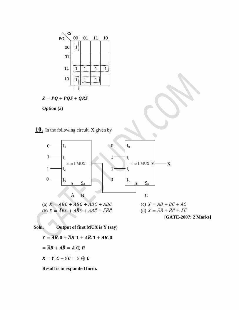
𝒁 = 𝑷𝑸 + 𝑷�̅�𝑺 + �̅��̅��̅�
Option (a)
10. In the following circuit, X given by
A B
4 to 1 MUX
S0S1
I0
I1
I2
I3
C
4 to 1 MUX
S0S1
I0
I1
I2
I3
Y X
0
1
1
0
0
1
1
0
(a) 𝑋 = 𝐴�̅�𝐶̅ + �̅�𝐵𝐶̅ + �̅��̅�𝐶 + 𝐴𝐵𝐶
(b) 𝑋 = �̅�𝐵𝐶 + 𝐴�̅�𝐶 + 𝐴𝐵𝐶̅ + �̅��̅�𝐶̅
(c) 𝑋 = 𝐴𝐵 + 𝐵𝐶 + 𝐴𝐶
(d) 𝑋 = �̅��̅� + �̅�𝐶̅ + �̅�𝐶̅
[GATE-2007: 2 Marks]
Soln. Output of first MUX is Y (say)
𝒀 = �̅��̅�. 𝟎 + �̅�𝑩. 𝟏 + 𝑨�̅�. 𝟏 + 𝑨𝑩. 𝟎
= �̅�𝑩 + 𝑨�̅� = 𝑨 ⊕ 𝑩
𝑿 = �̅�. 𝑪 + 𝒀�̅� = 𝒀 ⊕ 𝑪
Result is in expanded form.

𝑿 = (�̅�𝑩 + 𝑨�̅�)̅̅ ̅̅ ̅̅ ̅̅ ̅̅ ̅̅ ̅̅ ̅. 𝑪 + (�̅�𝑩 + 𝑨�̅�). �̅�
= �̅�𝑩̅̅ ̅̅ . 𝑨�̅�̅̅ ̅̅ . 𝑪 + �̅�𝑩�̅� + 𝑨�̅��̅�
= (𝑨 + �̅�)(�̅� + 𝑩)𝑪 + �̅�𝑩�̅� + 𝑨�̅��̅�
𝑨𝑩𝑪 + �̅��̅�𝑪 + �̅�𝑩�̅� + 𝑨�̅�𝑪
Option (a)
11. The Boolean function f implemented in the figure using two input multiplexers is
C
C
B
0
A
E
f
0
1 1
0
(a) 𝐴�̅�𝐶 + 𝐴𝐵𝐶̅
(b) 𝐴𝐵𝐶 + 𝐴�̅�𝐶̅
(c) �̅�𝐵𝐶 + �̅��̅�𝐶̅
(d) 𝐴𝐵̅̅ ̅̅ 𝐶 + �̅�𝐵𝐶̅
[GATE-2005: 1 Mark]
Soln. The output E can written as
𝑬 = �̅�𝑪 + 𝑩�̅�
Output f can be written as
𝒇 = �̅�. 𝟎 + 𝑬𝑨 = 𝑬. 𝑨
So, 𝒇 = 𝑬𝑨 = 𝑨�̅�𝑪 + 𝑨𝑩�̅�
Option (a)
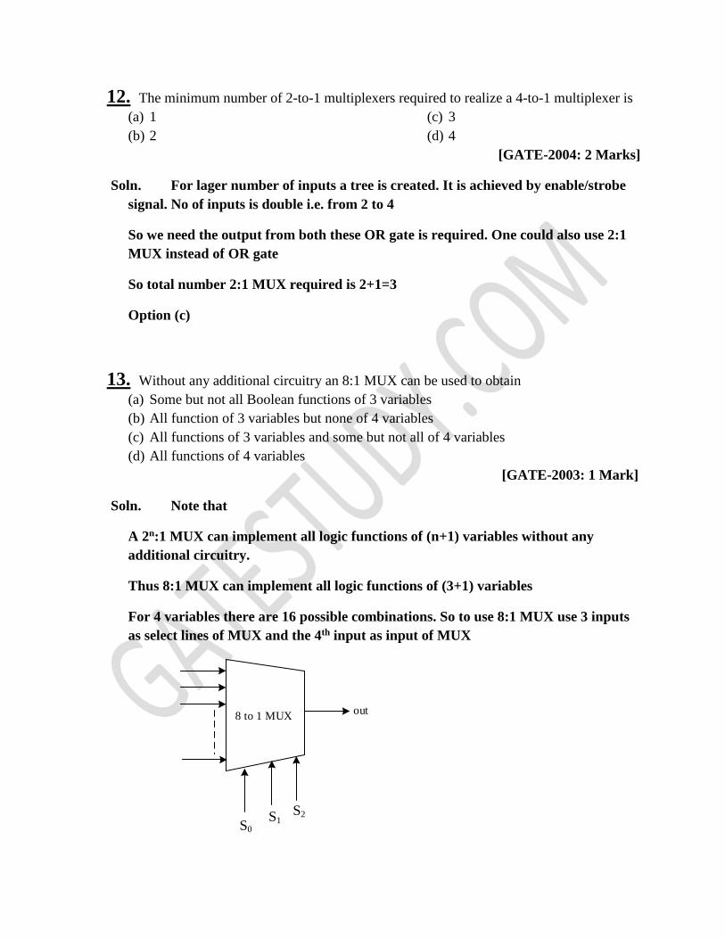
12. The minimum number of 2-to-1 multiplexers required to realize a 4-to-1 multiplexer is
(a) 1
(b) 2
(c) 3
(d) 4
[GATE-2004: 2 Marks]
Soln. For lager number of inputs a tree is created. It is achieved by enable/strobe
signal. No of inputs is double i.e. from 2 to 4
So we need the output from both these OR gate is required. One could also use 2:1
MUX instead of OR gate
So total number 2:1 MUX required is 2+1=3
Option (c)
13. Without any additional circuitry an 8:1 MUX can be used to obtain
(a) Some but not all Boolean functions of 3 variables
(b) All function of 3 variables but none of 4 variables
(c) All functions of 3 variables and some but not all of 4 variables
(d) All functions of 4 variables
[GATE-2003: 1 Mark]
Soln. Note that
A 2n:1 MUX can implement all logic functions of (n+1) variables without any
additional circuitry.
Thus 8:1 MUX can implement all logic functions of (3+1) variables
For 4 variables there are 16 possible combinations. So to use 8:1 MUX use 3 inputs
as select lines of MUX and the 4th input as input of MUX
8 to 1 MUX
S0
S1S2
out
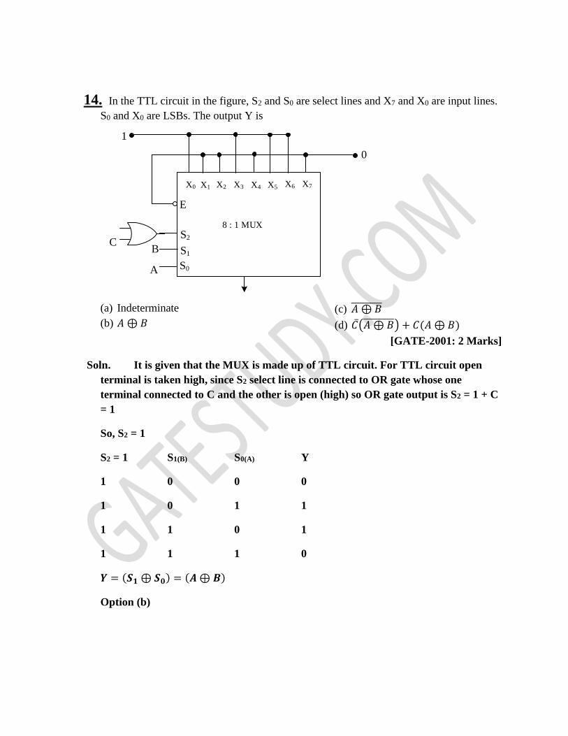
14. In the TTL circuit in the figure, S2 and S0 are select lines and X7 and X0 are input lines.
S0 and X0 are LSBs. The output Y is
X0 X1 X2 X3 X4 X5 X6 X7
E
S0
S1
S2
A
BC
8 : 1 MUX
0
1
(a) Indeterminate
(b) 𝐴 ⊕ 𝐵
(c) 𝐴 ⊕ 𝐵̅̅ ̅̅ ̅̅ ̅̅
(d) 𝐶̅(𝐴 ⊕ 𝐵̅̅ ̅̅ ̅̅ ̅̅ ) + 𝐶(𝐴 ⊕ 𝐵)
[GATE-2001: 2 Marks]
Soln. It is given that the MUX is made up of TTL circuit. For TTL circuit open
terminal is taken high, since S2 select line is connected to OR gate whose one
terminal connected to C and the other is open (high) so OR gate output is S2 = 1 + C
= 1
So, S2 = 1
S2 = 1 S1(B) S0(A) Y
1 0 0 0
1 0 1 1
1 1 0 1
1 1 1 0
𝒀 = (𝑺𝟏 ⊕ 𝑺𝟎) = (𝑨 ⊕ 𝑩)
Option (b)

15. The logic realized by the circuit shown in figure is
A B
4 to 1 MUX
S0S1
I0
I1
I2
I3
C
C
F
(a) 𝐹 = 𝐴ʘ𝐶
(b) 𝐹 = 𝐴 ⊕ 𝐶
(c) 𝐹 = 𝐵ʘ𝐶
(d) 𝐹 = 𝐵 ⊕ 𝐶
Soln. Output F is given by
𝑭 = �̅��̅�𝑪 + �̅�𝑩𝑪 + 𝑨�̅��̅� + 𝑨𝑩�̅�
= �̅�𝑪(�̅� + 𝑩) + 𝑨�̅�(�̅� + 𝑩)
= �̅�𝑪 + 𝑨�̅�
= (𝑨 ⊕ 𝑪)
Option (b)

Code Convertors
16. The circuit shown in the figure converts
MSB
MSB
OUTPUTS
INPUTS
(a) BCD to binary code
(b) Binary to excess-3 code
(c) Excess-3 to Gray code
(d) Gray to Binary code
[GATE-2003: 2 Marks]
Soln. The circuit is a code converter i.e. converts input bit code to some other code. It uses EX-
OR gates, and the inputs to EX-OR are from the input bit and output bit. So the guess is
that the circuit is for gray to binary converter. Take some simple input bits and verify
1 0 1 0
1 1 0 0
+ + +
Gray
Binary
Ex. 1
0 1 1 0
0 1 0 0
+ + +
Gray
Binary
Ex. 2
Note that EX-OR gate is modulo 2 adder.
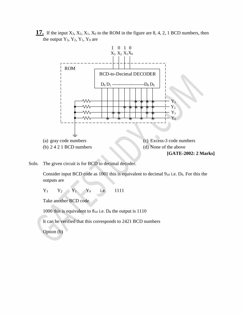
17. If the input X3, X2, X1, X0 to the ROM in the figure are 8, 4, 2, 1 BCD numbers, then
the output Y3, Y2, Y1, Y0 are
BCD-to-Decimal DECODER
D0 D1 ----------------------D8 D9
ROM
X3 X2 X1X0
1 0 1 0
Y3
Y2
Y1
Y0
**
***
*
*
* **
**
*
**
****
(a) gray code numbers
(b) 2 4 2 1 BCD numbers
(c) Excess-3 code numbers
(d) None of the above
[GATE-2002: 2 Marks]
Soln. The given circuit is for BCD to decimal decoder.
Consider input BCD code as 1001 this is equivalent to decimal 910 i.e. D9. For this the
outputs are
Y3 Y2 Y1 Y0 i.e. 1111
Take another BCD code.
1000 this is equivalent to 810 i.e. D8 the output is 1110
It can be verified that this corresponds to 2421 BCD numbers
Option (b)


