Copyright 2001, Agrawal & Bushnell
VLSI Test: Lecture 17 1
Lecture 17Analog Circuit Test --
A/D and D/A Converters
Lecture 17Analog Circuit Test --
A/D and D/A Converters
Motivation Present state-of-the-art Advantages of DSP-based analog tester Components of DSP-based analog tester Static A/D converter test Static D/A converter test Summary

Copyright 2001, Agrawal & Bushnell
VLSI Test: Lecture 17 2
Mixed-Signal Testing Problem
Mixed-Signal Testing Problem

Copyright 2001, Agrawal & Bushnell
VLSI Test: Lecture 17 3
MotivationMotivation Mixed-signal (analog + digital) ICs more
common Wireless, networking, multi-media, real-time
control – explosive growth Digital core (Digital Signal Processor (DSP)
and processor) surrounded by A/Ds, filters, D/As, MEMs devices
Less distance between transducer and measurement point – less noise
More linear, less non-linear analog circuitry Move non-linear function into DSP unit Easier to test Analog MOS devices run in transistor
saturation mode Mixed-signal has testing observability problem
Copyright 2001, Agrawal & Bushnell
VLSI Test: Lecture 17 4
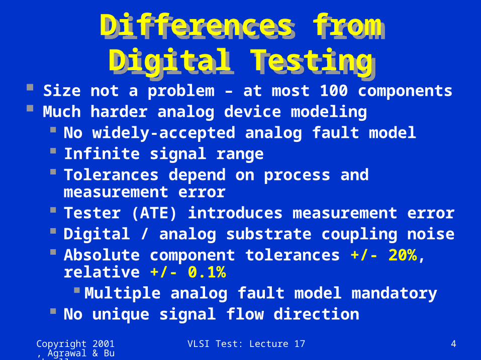
Differences from Digital Testing
Differences from Digital Testing
Size not a problem – at most 100 components Much harder analog device modeling
No widely-accepted analog fault model Infinite signal range Tolerances depend on process and
measurement error Tester (ATE) introduces measurement error Digital / analog substrate coupling noise Absolute component tolerances +/- 20%,
relative +/- 0.1% Multiple analog fault model mandatory
No unique signal flow direction
Copyright 2001, Agrawal & Bushnell
VLSI Test: Lecture 17 5
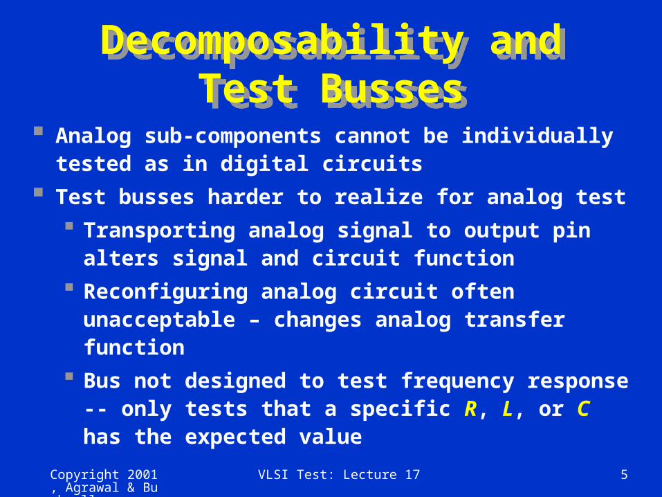
Decomposability and Test Busses
Decomposability and Test Busses
Analog sub-components cannot be individually tested as in digital circuits
Test busses harder to realize for analog test
Transporting analog signal to output pin alters signal and circuit function
Reconfiguring analog circuit often unacceptable – changes analog transfer function
Bus not designed to test frequency response -- only tests that a specific R, L, or C has the expected value

Copyright 2001, Agrawal & Bushnell
VLSI Test: Lecture 17 6
Present-Day Analog Testing Methods
Present-Day Analog Testing Methods
Specification-based (functional) tests
Main method for analog – tractable and does not need an analog fault model
Intractable for digital -- # tests is huge
Structural ATPG – used for digital, just beginning to be used for analog (exists)
Separate test for functionality and timing not possible in analog circuit
Possible in digital circuit

Copyright 2001, Agrawal & Bushnell
VLSI Test: Lecture 17 7
DSP-Based Tester Benefits over Analog Tester
DSP-Based Tester Benefits over Analog Tester
More accurate Reduces crosstalk, noise, signal drift Less non-linearity Component aging less troublesome Thermal effects less troublesome Faster when making multiple
measurements Eliminates filter settling time of analog
Automatic Test Equipment (ATE) More repeatable testing Easier calibration More measurement information provided Smaller, cheaper, and uses less power
Copyright 2001, Agrawal & Bushnell
VLSI Test: Lecture 17 8
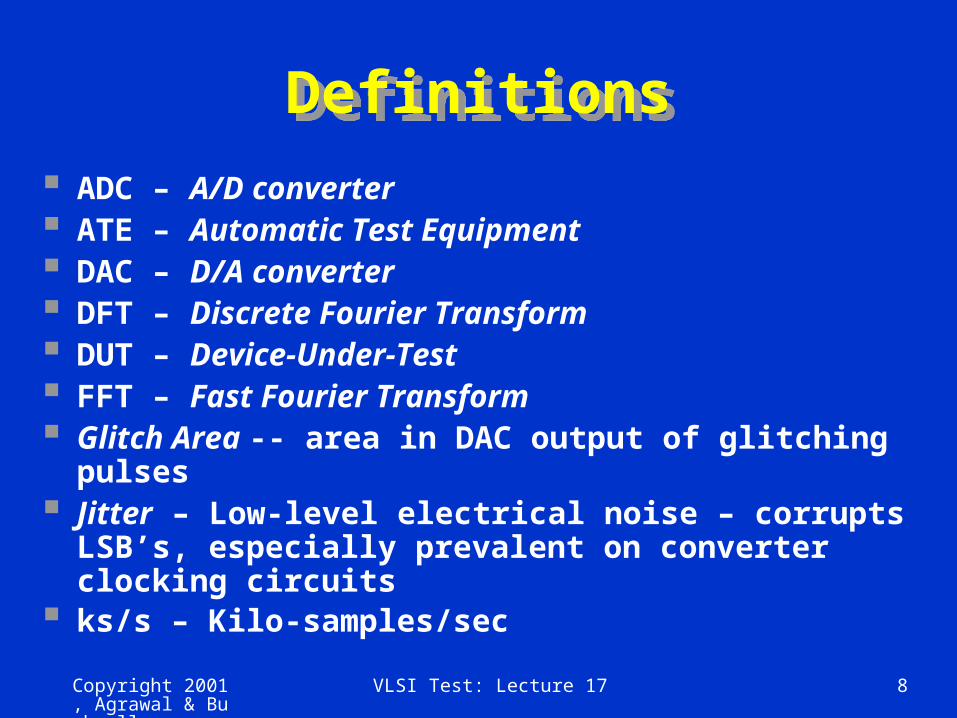
DefinitionsDefinitions
ADC – A/D converter ATE – Automatic Test Equipment DAC – D/A converter DFT – Discrete Fourier Transform DUT – Device-Under-Test FFT – Fast Fourier Transform Glitch Area -- area in DAC output of glitching
pulses Jitter – Low-level electrical noise – corrupts
LSB’s, especially prevalent on converter clocking circuits
ks/s – Kilo-samples/sec

Copyright 2001, Agrawal & Bushnell
VLSI Test: Lecture 17 9
More DefinitionsMore Definitions LSB -- Least Significant Bit (of converter) Measurement – Result of measuring O/P
analog parameter and quantifying it Measurement Error – Introduced by
measurement process Non-Deterministic Device – All analog
circuit measurements are not repeatable due to DUT or tester measurement noise
Phase-Locked-Loop – Clock circuit with feedback to keep desired signal phase
Settling Time -- Time for DAC reconstruction filter to settle
Test – Combination of analog stimulus, measurement of voltage or current, with a measurement error tolerance

Copyright 2001, Agrawal & Bushnell
VLSI Test: Lecture 17 10
Analog Tester Concept© 1987 IEEE
Analog Tester Concept© 1987 IEEE

Copyright 2001, Agrawal & Bushnell
VLSI Test: Lecture 17 11
DSP Tester Concept© 1987 IEEE
DSP Tester Concept© 1987 IEEE

Copyright 2001, Agrawal & Bushnell
VLSI Test: Lecture 17 12
DSP Tester Characteristics
DSP Tester Characteristics
Very fast DSP array processor Needs 31 bits precision – double-
precision N = number of samples Signal / quantization noise of entire
vector
N times better than that of 1 sample
Copyright 2001, Agrawal & Bushnell
VLSI Test: Lecture 17 13
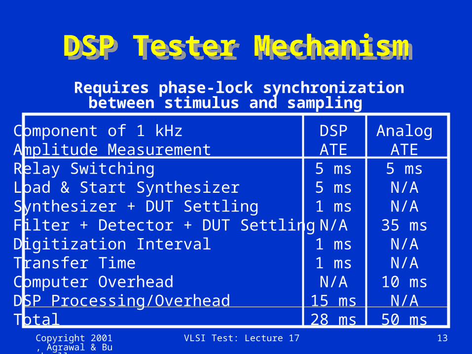
DSP Tester MechanismDSP Tester MechanismRequires phase-lock synchronization
between stimulus and sampling
Component of 1 kHzAmplitude MeasurementRelay SwitchingLoad & Start SynthesizerSynthesizer + DUT SettlingFilter + Detector + DUT SettlingDigitization IntervalTransfer TimeComputer OverheadDSP Processing/OverheadTotal
AnalogATE5 msN/AN/A
35 msN/AN/A
10 msN/A
50 ms
DSPATE5 ms5 ms1 msN/A
1 ms1 msN/A
15 ms28 ms

Copyright 2001, Agrawal & Bushnell
VLSI Test: Lecture 17 14
Waveform Synthesis© 1987 IEEE
Waveform Synthesis© 1987 IEEE
Needs sin x / x (sinc) correction – Finite sample width

Copyright 2001, Agrawal & Bushnell
VLSI Test: Lecture 17 15
Waveform Sampling© 1987 IEEE
Waveform Sampling© 1987 IEEE
Sampling rate > 100 ks/s

Copyright 2001, Agrawal & Bushnell
VLSI Test: Lecture 17 16
ATE Clock GeneratorATE Clock GeneratorWS = waveform source WM = waveform measurement

Copyright 2001, Agrawal & Bushnell
VLSI Test: Lecture 17 17
Cadence Test Programming Language
Cadence Test Programming Language
set master clock to <double> <int>
connect dp master clock
to pm line <word1>
clock ws main mem with pm clock <word1> divide by <word2>
set wm to pm clk <word1> divide by <word2>
12
frequencyperiod
timesover
internal referencedoubled reference
source1source2
{ }

Copyright 2001, Agrawal & Bushnell
VLSI Test: Lecture 17 18
A/D and D/A Converter Static Testing MethodsA/D and D/A Converter Static Testing Methods
Copyright 2001, Agrawal & Bushnell
VLSI Test: Lecture 17 19
A/D and D/A Test Parameters
A/D and D/A Test Parameters
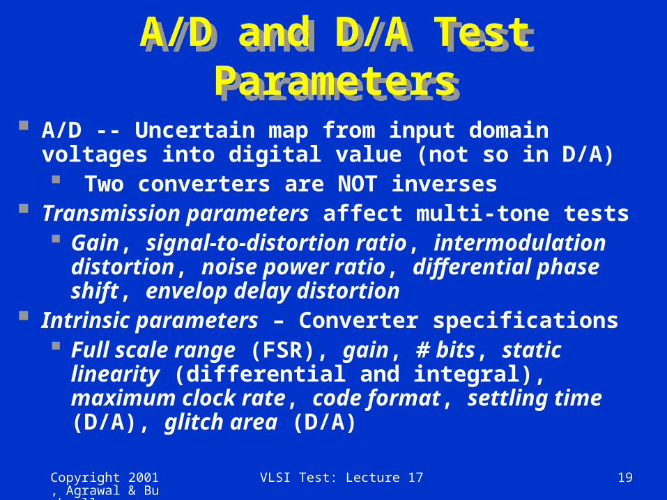
A/D -- Uncertain map from input domain voltages into digital value (not so in D/A) Two converters are NOT inverses
Transmission parameters affect multi-tone tests Gain, signal-to-distortion ratio,
intermodulation distortion, noise power ratio, differential phase shift, envelop delay distortion
Intrinsic parameters – Converter specifications Full scale range (FSR), gain, # bits, static
linearity (differential and integral), maximum clock rate, code format, settling time (D/A), glitch area (D/A)

Copyright 2001, Agrawal & Bushnell
VLSI Test: Lecture 17 20
Ideal Transfer Functions
Ideal Transfer Functions
A/D Converter D/A Converter

Copyright 2001, Agrawal & Bushnell
VLSI Test: Lecture 17 21
Offset ErrorOffset Error

Copyright 2001, Agrawal & Bushnell
VLSI Test: Lecture 17 22
Gain ErrorGain Error
Copyright 2001, Agrawal & Bushnell
VLSI Test: Lecture 17 23
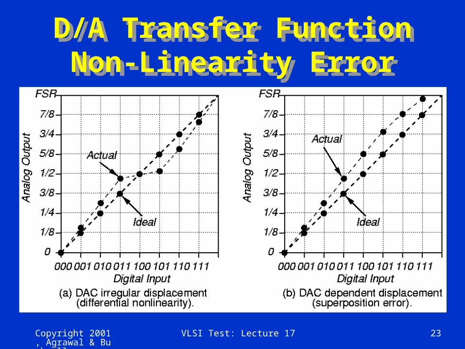
D/A Transfer Function Non-Linearity Error
D/A Transfer Function Non-Linearity Error

Copyright 2001, Agrawal & Bushnell
VLSI Test: Lecture 17 24
Flash A/D ConverterFlash A/D Converter

Copyright 2001, Agrawal & Bushnell
VLSI Test: Lecture 17 25
Static Linearity TestStatic Linearity Test

Copyright 2001, Agrawal & Bushnell
VLSI Test: Lecture 17 26
Static Linear HistogramStatic Linear Histogram
Code Count
DLE (LSBfraction)DNLTransferChar.(counts)ILE (LSBfraction)INL
T (0)3 + 3 = 6
D (0)-0.1176
C (0)0
E (0)0
T (1)5
D (1)-0.265
C (1)5.5
E (1)-0.191
T (2)4
D (2)-0.412
C (2)10
E (2)-0.529
T (3)11
D (3)0.618
C (3)17.5
E (3)-0.427
T (4)8
D (4)0.177
C (4)27
E (4)-0.030
DNL and INL in RMS LSB
0.3650
0.3161

Copyright 2001, Agrawal & Bushnell
VLSI Test: Lecture 17 27
Differential Linearity Error
Differential Linearity Error
Differential linearity function – How each code step differs from ideal or average step (by code number), as fraction of LSB
Subtract average count for each code tally, express that in units of LSBs
Repeat test waveform 100 to 150 times, use slow triangle wave to increase resolution

Copyright 2001, Agrawal & Bushnell
VLSI Test: Lecture 17 28
Example DLE Function© 1987 IEEE
Example DLE Function© 1987 IEEE
Code
DLE

Copyright 2001, Agrawal & Bushnell
VLSI Test: Lecture 17 29
Integral Linearity Error (ILE)
© 1987 IEEE
Integral Linearity Error (ILE)
© 1987 IEEEILE [i] = ILE [i – 1] x DLE [i] + DLE [i – 1]
2( )

Copyright 2001, Agrawal & Bushnell
VLSI Test: Lecture 17 30
Linear Histogram and DLE of 8-bit ADC
© 1987 IEEE
Linear Histogram and DLE of 8-bit ADC
© 1987 IEEE

Copyright 2001, Agrawal & Bushnell
VLSI Test: Lecture 17 31
Sinusoidal Histogram© 1987 IEEE
Sinusoidal Histogram© 1987 IEEE
Catches sparkle and glitch codes
N (# samples)2 – 4 xthat forlinearhistogram
Copyright 2001, Agrawal & Bushnell
VLSI Test: Lecture 17 32
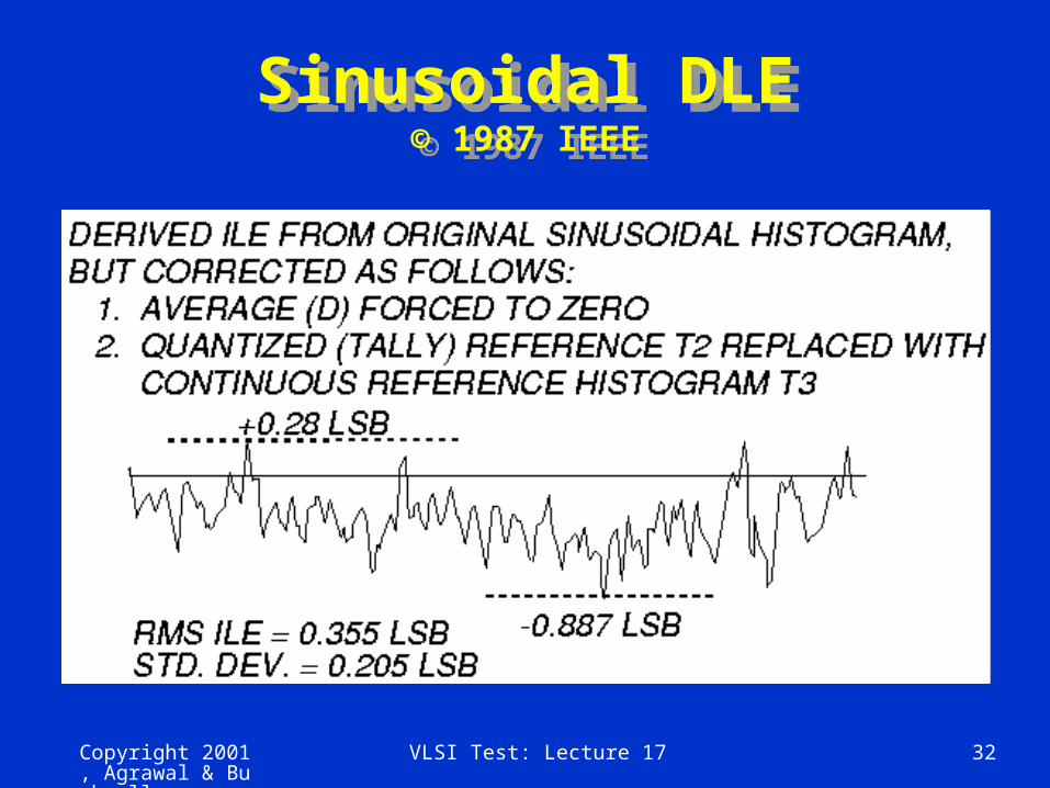
Sinusoidal DLE© 1987 IEEE
Sinusoidal DLE© 1987 IEEE

Copyright 2001, Agrawal & Bushnell
VLSI Test: Lecture 17 33
D/A Differential Test Fixture© 1987 IEEE
D/A Differential Test Fixture© 1987 IEEE
Measure Vy – Vx difference, not absolute Vx or Vy

Copyright 2001, Agrawal & Bushnell
VLSI Test: Lecture 17 34
SummarySummary DSP-based tester has:
Waveform Generator Waveform Digitizer High frequency clock with dividers for
synchronization A/D and D/A Test Parameters
Transmission Intrinsic
A/D and D/A Faults: offset, gain, non-linearity errors Measured by DLE, ILE, DNL, and INL
A/D Test Histograms – static linear and sinusoidal D/A Test –- Differential Test Fixture


