University of South FloridaScholar Commons
Graduate Theses and Dissertations Graduate School
2007
Effect of temperature on copper chemicalmechanical planarizationVeera Raghava R KakireddyUniversity of South Florida
Follow this and additional works at: http://scholarcommons.usf.edu/etd
Part of the American Studies Commons
This Thesis is brought to you for free and open access by the Graduate School at Scholar Commons. It has been accepted for inclusion in GraduateTheses and Dissertations by an authorized administrator of Scholar Commons. For more information, please contact [email protected].
Scholar Commons CitationKakireddy, Veera Raghava R, "Effect of temperature on copper chemical mechanical planarization" (2007). Graduate Theses andDissertations.http://scholarcommons.usf.edu/etd/2236

Effect of Temperature on Copper Chemical Mechanical Planarization
by
Veera Raghava R. Kakireddy
A thesis submitted in partial fulfillment of the requirements for the degree of
Master of Science in Electrical Engineering Department of Electrical Engineering
College of Engineering University of South Florida
Co-Major Professor: Ashok Kumar, Ph.D. Co-Major Professor: Shekhar Bhansali, Ph.D.
Wilfrido Moreno, Ph.D.
Date of Approval: March 28, 2007
Keywords: cof, dishing, defects, pad, metal
© Copyright 2007, Veera Raghava R. Kakireddy

Dedication
I dedicate this work to my beloved parents, family and my friends.

ACKNOWLEDMENTS
I am thankful to everyone who helped me throughout my research work to make
this work successful. I thank my family for their love and constant support. I express my
deep gratitude and thankfulness to Dr. Ashok Kumar, Major Professor, for providing me
with this opportunity to conduct the thesis and also for his guidance and encouragement
throughout my research work. I am grateful to Dr. Shekhar Bhansali, Co-major Professor
and Dr. Wilfrido Moreno for accepting to be on the committee. I am very thankful to my
colleagues and friends in the group, Raghu Mudhivarthi for his valuable suggestions and
help during the research work and Sathyaharish Jeedigunta for his support and
encouragement. I thank all my friends for their encouragement and moral support during
the research period.

i
Table of Contents
List of Tables iii
List of Figures iv
Abstract vii
Chapter 1 Introduction 1 1.1 Multilevel Metallization and I.C’s 1 1.2 Why CMP 2 1.3 Literature Overview 6 1.4 Thesis Outline 10
Chapter 2 Understanding CMP 11 2.1 The CMP Process 11 2.2 Factors Affecting CMP 13 2.2.1 Polishing Pad 13 2.2.2 Slurry 14 2.2.3 Surface Under Polish 16 2.2.4 Pressure 16 2.2.5 Velocity 17 2.2.6 Temperature 17 2.3 Copper Significance 18
2.4 Copper Deposition Techniques 20 2.4.1 Chemical Vapor Deposition (CVD) 20 2.4.2 Physical Vapor Deposition (PVD) 21 2.4.3 Copper Electroplating 22 2.4.4 Electroless-Plating 23
2.5 Copper Removal Mechanism 24 2.5.1 Formation of Surface Layer 25 2.5.2 Abrasion 26 2.5.3 Removal of Abraded Material 26 2.6 Pattern Geometry Effects on Removal Mechanism 27 2.7 Defects During CMP 27 2.7.1 Dishing 28 2.7.2 Erosion 29 2.7.3 Total Copper/Metal Loss 30 2.7.4 Scratches 30 2.7.5 Wafer to Wafer Non-uniformity 31

ii
2.7.6 Within Wafer Non-uniformity 31 2.8 Summary 31
Chapter 3 Experimental 33 3.1 CMP Testing Tool 33
3.2 CMP Consumables 34 3.3 Experimental Parameters 35 3.4 Estimation of Removal Rate 37 3.5 Post CMP Analysis/Characterization Tools 39 3.5.1 Profilometer 39 3.5.2 Atomic Force Microscopy (AFM) 40 3.5.3 Scanning Electron Microscopy (SEM) 41 3.5.4 Dynamic Mechanical Analysis (DMA) 43 3.5.5 X-Ray Diffraction (XRD) 45 3.6 Summary 47
Chapter 4 Results and Discussion 48 4.1 Dynamic Mechanical Analysis (DMA) of Pads 48 4.2 Scanning Electron Microscopy (SEM) Analysis 50 4.3 Analysis of COF and Removal Rate with Slurry Temperature and Pad 52 4.3.1 Coefficient of Friction (COF) 52 4.3.2 Removal Rate 59 4.4 Analysis of Dishing with Slurry Temperature and Pad 62
4.5 Analysis of Metal Loss with Slurry Temperature and Pad 69 4.6 Analysis of Adhesion Failure and Mechanical Properties with Slurry Temperature 71 4.7 Analysis of Electrical Properties with Slurry Temperature 76 4.8 Summary 80
Chapter 5 Conclusions and Future Work 82 5.1 Conclusions 82 5.1.1 Friction (COF) and Removal Rate Studies 82 5.1.2 Dishing and Metal Loss 83 5.1.3 Film Mechanical and Electrical Properties 85 5.2 Future Work 85
References 87

iii
List of Tables Table 2.1 Comparison of Properties of Metals 18
Table 3.1 Consumables and Process Parameters for Polishing 35
Table 4.1 Coefficient of Friction at Different Slurry Temperatures Using Slurry-1 57
Table 4.2 Coefficient of Friction at Different Slurry Temperatures Using Slurry-2 58
Table 4.3 Removal Rates at Different Slurry Temperatures Using Slurry 1 and 2 60
Table 4.4 Normalized Dishing Data on Metal Lines and Bond Pads 62
Table 4.5 Mechanical Properties of Copper Thin Films Before and After Polishing 74
iv
List of Figures Figure 1.1 Cross Section of a Device Showing Various Levels of Metallization 2
Figure 1.2 2005 ITRS – Half Pitch and Gate Length Trends 3
Figure 1.3 Schematic of a CMP Setup 6
Figure 2.1 Schematic of a CVD Process 21
Figure 2.2 Schematic of a PVD Process 22
Figure 2.3 Schematic of a Copper Electroplating System 23
Figure 2.4 Schematic of Copper Removal Mechanism 24
Figure 2.5 Defects Formed During CMP 28
Figure 2.6 Schematic of Copper Dishing During CMP 29
Figure 2.7 Schematic of Erosion Profile 30
Figure 3.1 CMP Bench Top Tester 34
Figure 3.2 Process Flow Diagram for Fabricating the PMOS Devices 37
Figure 3.3 COF vs. Time Graph Used to Estimate Removal Rate 39
Figure 3.4 Schematic of a Profilometer Scan 40
Figure 3.5 Schematic of Operation of an AFM 41
Figure 3.6 SEM Image/Schematic of an AFM Cantilever Tip 41
Figure 3.7 Block Diagram Showing the Operation of a SEM 43
Figure 3.8 DMA 2980 Instrument at USF 45
Figure 3.9 Schematic of an X-Ray Diffractometer 46
Figure 4.1 Storage Modulus and Tan Delta vs. Temperature at 10 Hz Frequency 49
v
Figure 4.2 Loss Modulus vs. Temperature at 10 Hz Frequency 50
Figure 4.3 SEM Image of Pad A - a) Unconditioned b) Conditioned 51
Figure 4.4 SEM Image of Pad B - a) Unconditioned b) Conditioned 51
Figure 4.5 COF vs. Time of a Sample at 15 °C on Pad A 52
Figure 4.6 COF vs. Time of a Sample at 20 °C on Pad A 53
Figure 4.7 COF vs. Time of a Sample at 25 °C on Pad A 53
Figure 4.8 COF vs. Time of a Sample at 30 °C on Pad A 54
Figure 4.9 COF vs. Time of a Sample at 35 °C on Pad A 54
Figure 4.10 COF vs. Time of a sample at 15 °C on Pad B 55
Figure 4.11 COF vs. Time of a sample at 20 °C on Pad B 55
Figure 4.12 COF vs. Time of a sample at 25 °C on Pad B 56
Figure 4.13 COF vs. Time of a sample at 30 °C on Pad B 56
Figure 4.14 COF vs. Time of a sample at 35 °C on Pad B 57
Figure 4.15 Change in COF vs. Slurry Temperature for Slurry-1 58
Figure 4.16 Change in COF vs. Slurry Temperature for Slurry-2 59
Figure 4.17 Removal Rate vs. Slurry Temperature Using Slurry-1 60
Figure 4.18 Removal Rate vs. Slurry Temperature Using Slurry-2 61
Figure 4.19 Dishing on a 10 µm Wide Metal Line vs. Slurry Temperature Using Slurry-1 63
Figure 4.20 Dishing on a 10 µm Wide Metal Line vs. Slurry Temperature Using Slurry-2 64
Figure 4.21 Dishing on a 20 µm Wide Metal Line vs. Slurry Temperature Using Slurry-1 65
Figure 4.22 Dishing on a 20 µm Wide Metal Line vs. Slurry Temperature Using Slurry-2 65

vi
Figure 4.23 Dishing on a 50 µm Wide Metal Line vs. Slurry Temperature Using Slurry-1 66
Figure 4.24 Dishing on a 50 µm Wide Metal Line vs. Slurry Temperature Using Slurry-2 67
Figure 4.25 Dishing on a 100 µm Bond Pad vs. Slurry Temperature Using Slurry –1 68
Figure 4.26 Dishing on a 100 µm Bond Pad vs. Slurry Temperature Using Slurry –2 68
Figure 4.27 Dishing Profiles of Metal Lines of Different Widths 69
Figure 4.28 Metal Loss vs. Slurry Temperature Using Slurry-1 70
Figure 4.29 Metal Loss vs. Slurry Temperature Using Slurry-2 71
Figure 4.30 Pictures Showing Peeling on Wafers Polished at Different Temperatures 72
Figure 4.31 Graphs Showing XRD Peaks on Copper Wafers Polished at Different Temperatures 73
Figure 4.32 Hardness vs. Displacement into Surface for Unpolished and Polished Copper Samples 75
Figure 4.33 Modulus vs. Displacement into Surface for Polished and Unpolished Copper Samples 75
Figure 4.34 Graphs Showing Transfer Curves (I-V Characteristics) of Wafers Polished at Different Temperatures 77
Figure 4.35 Graphs Showing Sub-Threshold Log Plot Curves (I-V Characteristics) of Wafers Polished at Different Temperature 79
vii
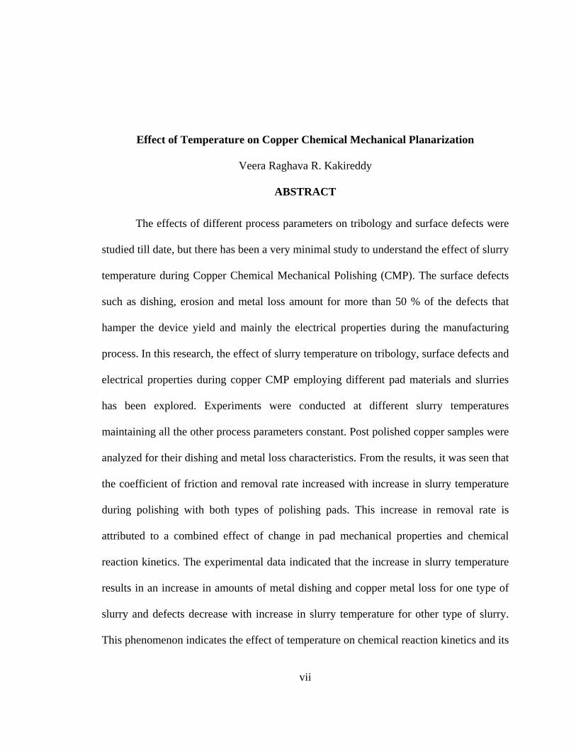
Effect of Temperature on Copper Chemical Mechanical Planarization
Veera Raghava R. Kakireddy
ABSTRACT
The effects of different process parameters on tribology and surface defects were
studied till date, but there has been a very minimal study to understand the effect of slurry
temperature during Copper Chemical Mechanical Polishing (CMP). The surface defects
such as dishing, erosion and metal loss amount for more than 50 % of the defects that
hamper the device yield and mainly the electrical properties during the manufacturing
process. In this research, the effect of slurry temperature on tribology, surface defects and
electrical properties during copper CMP employing different pad materials and slurries
has been explored. Experiments were conducted at different slurry temperatures
maintaining all the other process parameters constant. Post polished copper samples were
analyzed for their dishing and metal loss characteristics. From the results, it was seen that
the coefficient of friction and removal rate increased with increase in slurry temperature
during polishing with both types of polishing pads. This increase in removal rate is
attributed to a combined effect of change in pad mechanical properties and chemical
reaction kinetics. The experimental data indicated that the increase in slurry temperature
results in an increase in amounts of metal dishing and copper metal loss for one type of
slurry and defects decrease with increase in slurry temperature for other type of slurry.
This phenomenon indicates the effect of temperature on chemical reaction kinetics and its

viii
influence on defect generation. This can be attributed due to the change in pad asperities
due to change in pad mechanical properties and chemical kinetics with change in slurry
temperature. The slurry temperature has an effect not only on the surface defects and
tribology but also on the change in pad mechanical properties. The copper thin films
peeled off at higher polishing temperatures, leading to adhesion failure. With increase in
temperature the copper crystallinity, hardness and modulus increased. Further with
increase in the defects the electrical properties of the devices also degraded drastically
and even failed to operate at higher levels of dishing and metal loss. This research is
aimed at understanding the physics governing the defect generation during CMP.
1
Chapter 1
Introduction
1.1 Multilevel Metallization and I.C’s
Shrinking device dimension’s associated with ultra large scale integrated circuits
is highly effective in achieving high speed performance and in increasing yields at lower
cost per chip With the ever increasing thirst to build faster chips the industry is facing the
critical problem of integrating the new design rules and also in advancing the Moore’s
law further. In order to achieve higher circuit density the number of interconnect layers
are increased. However when the devices are scaled down the performance falls down as
a result for higher circuit density. The higher circuit density causes the devices to slow
down due to the increase in interconnect RC time delay of the circuit. As more and more
faster devices are built the complexity of fabricating the device with more interconnect
layers also increases [1]. In order to assure the performance of the high speed circuits,
continuous efforts have been devoted for incorporating copper or low dielectric constant
materials into multilevel interconnections for reducing major part of circuit delay, cross
talk and power consumption. Till date Aluminum has been the choice of semiconductor
manufacturers for the metal contacts, but as aluminum has high resistivity the industry
had shifted to copper which has very low resitivity. Also copper has lower
electromigration when compared to aluminum. Unlike aluminum, copper cannot be
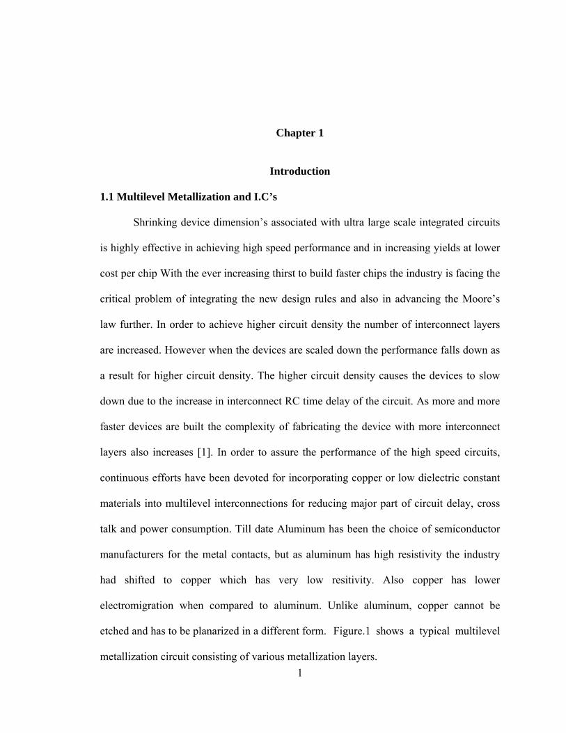
etched and has to be planarized in a different form. Figure.1 shows a typical multilevel
metallization circuit consisting of various metallization layers.
2
Figure 1.1 Cross Section of a Device Showing Various Levels of Metallization [2]
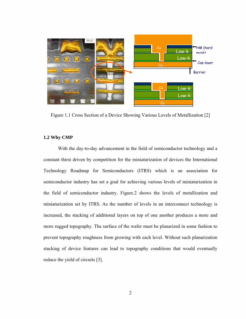
1.2 Why CMP
With the day-to-day advancement in the field of semiconductor technology and a
constant thirst driven by competition for the miniaturization of devices the International
Technology Roadmap for Semiconductors (ITRS) which is an association for
semiconductor industry has set a goal for achieving various levels of miniaturization in
the field of semiconductor industry. Figure.2 shows the levels of metallization and
miniaturization set by ITRS. As the number of levels in an interconnect technology is
increased, the stacking of additional layers on top of one another produces a more and
more rugged topography. The surface of the wafer must be planarized in some fashion to
prevent topography roughness from growing with each level. Without such planarization
stacking of device features can lead to topography conditions that would eventually
reduce the yield of circuits [3].
Cap layer
HM (hard mask)
Low-k Low-k
Cu Barrier
Cu
Low-k Low-k
Cu
Cu
3
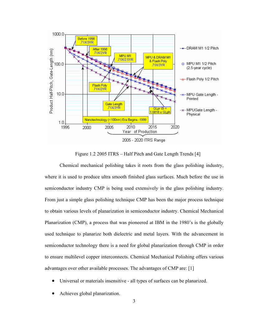
Figure 1.2 2005 ITRS – Half Pitch and Gate Length Trends [4]
Chemical mechanical polishing takes it roots from the glass polishing industry,
where it is used to produce ultra smooth finished glass surfaces. Much before the use in
semiconductor industry CMP is being used extensively in the glass polishing industry.
From just a simple glass polishing technique CMP has been the major process technique
to obtain various levels of planarization in semiconductor industry. Chemical Mechanical
Planarization (CMP), a process that was pioneered at IBM in the 1980’s is the globally
used technique to planarize both dielectric and metal layers. With the advancement in
semiconductor technology there is a need for global planarization through CMP in order
to ensure multilevel copper interconnects. Chemical Mechanical Polishing offers various
advantages over other available processes. The advantages of CMP are: [1]
• Universal or materials insensitive - all types of surfaces can be planarized.
• Achieves global planarization.
4
• Reduces severe topography allowing for fabrication with tighter design rules and
multilevel interconnects.
• Provides an alternate means to pattern metal thereby eliminating the need for
reactive ion etching or plasma etch for difficult to etch metals and alloys (Eg:
Copper).
• Leads to improved metal step coverage.
• Helps in improving reliability, speed and yield of devices.
• Does not use hazardous gases as in the case of dry etching process.
• Low cost process.
The CMP process even with many advantages and desired properties is not
without drawbacks such as dishing, erosion etc. Very little has been understood about the
effects of temperature during the CMP process. Even though research has been done to
study the temperature effect on pad not much has been done to study its affect on surface
defects and tribology [5].
Chemical mechanical polishing which is a process of chemical and mechanical
action on the surface being processed is dependent on various input process parameters.
CMP was initially developed for polishing oxide (SiO2), which was then used as the
interlevel dielectric (ILD) in the multilevel metallization. However with unprecedent
advancement in semiconductor technology and introduction of various new dielectric
materials, barrier layer materials and copper as metal the CMP development was forced
to follow a two fold approach to achieve the required level of planarization of various
layers. In this technique, high elevation features are selectively removed resulting in
surface with improved planarity [3].
5
The process of chemical mechanical polishing is performed by mounting the
wafer face down on a carrier, which is then forced against a platen with a polishing pad
of a polymer such as polyurethane. The carrier and the platen rotate relative motion to
each other [3]. A continuous flow of slurry containing abrasive particles is continuously
fed onto the surface of polishing pad while the wafer and pad rotate relative to each other.
The interaction of both chemical and mechanical effects results in material removal from
the wafer surface. The removal rate of the material during CMP is governed by the
Preston’s equation: [1]
Removal Rate (RR) = Kp * P * V (1.1)
Where P is the pressure applied on the wafer surface, Kp is the Preston’s
coefficient and V is the linear velocity of the pad relative to the wafer. Preston’s equation
is the most frequently referenced expression for polishing rates.
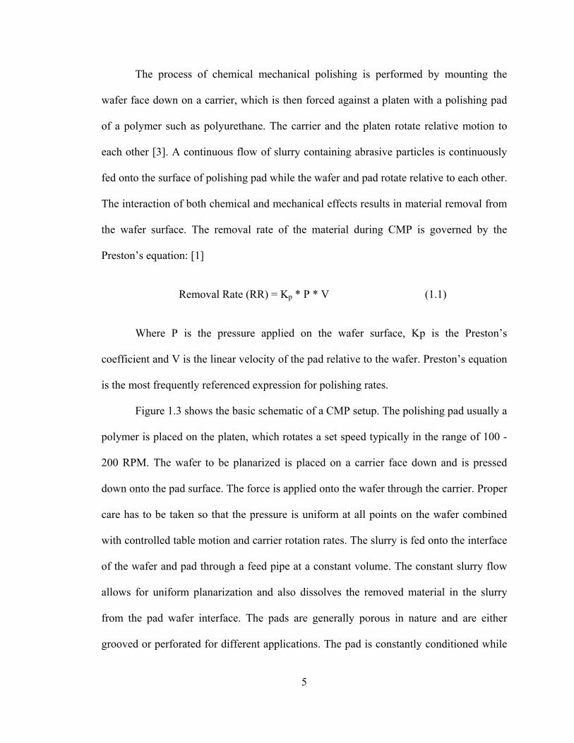
Figure 1.3 shows the basic schematic of a CMP setup. The polishing pad usually a
polymer is placed on the platen, which rotates a set speed typically in the range of 100 -
200 RPM. The wafer to be planarized is placed on a carrier face down and is pressed
down onto the pad surface. The force is applied onto the wafer through the carrier. Proper
care has to be taken so that the pressure is uniform at all points on the wafer combined
with controlled table motion and carrier rotation rates. The slurry is fed onto the interface
of the wafer and pad through a feed pipe at a constant volume. The constant slurry flow
allows for uniform planarization and also dissolves the removed material in the slurry
from the pad wafer interface. The pads are generally porous in nature and are either
grooved or perforated for different applications. The pad is constantly conditioned while
6
polishing in order to maintain its roughness. The conditioner is usually made of a
diamond grid.
Figure 1.3 Schematic of a CMP Setup
1.3 Literature Overview
With the ever increasing demand for faster performing devices and a constant
competition driven industry, till date vast research has been done on various aspects of
chemical mechanical polishing (CMP) and still research is being done investigating
various aspects of CMP which have been either not looked into or the aspects which
couldn’t be understood. Various materials are being investigated for use in semiconductor
devices. Different low-k dielectric materials have replaced the traditional silicon dioxide
(SiO2) which has a dielectric constant ~ 4 with materials of dielectric constant ~ 2.2.
Copper has replaced aluminum as the material for contact metal and interconnects.
Various reliability studies have been conducted on copper for multilevel metallization
Carrier
Wafer
Slurry
Platen (Pad Holder)
Pad
Pad Conditioner
Downforce
7
schemes. Chemical mechanical polishing has been the choice of semiconductor industry
and researchers for copper removal, as copper cannot be removed by conventional
techniques such as wet and dry etching.
Till date research has been done on the CMP of copper looking into various
aspects of polishing such as the consumables, process parameters and other input
parameters. The chemical mechanisms by which the planarization and removal occur
during the chemical mechanical polishing (CMP) of copper have been investigated long
back by Steigerwald et al [6]. They proposed that removal occurs as mechanical abrasion
of the surface under polish followed by dissolution of abraded particles. Chemical
Mechanical Polishing of copper using silica and alumina abrasive particles in different
chemistries has been studied by Carpio et al [7]. In their study the problems with
formulation of copper slurries were discussed. Slurries with different chemistries have
been studied for their reactivity with pad surfaces by Obeng et al [8]. The results showed
that the polyurethane pad material is incompatible with some of the chemicals used in
CMP, such as hydrogen peroxide. The influence of the slurry chemistry on frictional
force in copper during the CMP has been studied by Ishikawa et al [9]. Their study
showed that polishing rate increased non-linearly with frictional force, which is
controlled by the concentration of slurry chemical constituents.
The effect of slurry surfactant, abrasive size on tribology and kinetics in copper
CMP has been determined by Li et al [10]. The abrasive size was a significant factor
while surfactant containing formulations showed significant reduction in coefficient of
friction (COF). The effects of amount of concentration of abrasive particles were studied
by Nomura et al [11] and were found to have a significant affect on the polishing process.
8
CMP process of two different substrates using copper discs and copper were compared
by analyzing their COF’s, removal rate and pad temperature analysis by Li et al [12].
Their studies showed that the coefficient of friction and material removal rates were
higher for copper deposited wafers. The wear and tear in CMP polyurethane pads due the
physical and chemical changes have been analyzed by Lu et al [13]. Their results showed
changes in pore geometry of the CMP pads after use due to wear and tear. Properties of
CMP polishing pads before and after CMP have been studied using Dynamic Mechanical
Analysis (DMA) by Lu et al [14]. The studies showed that mechanical force has shown
more significance than chemical action in pad degradation.
The effect of pattern characteristics during copper CMP has been investigated by
Wang et al [15]. The copper and ILD CMP have been characterized by looking into some
thermal aspects by Sorooshian et al [16]. In their study a modified Preston’s equation has
been proposed by taking the temperature effect into consideration. A two step copper
removal method has been studied for removal of thick copper by Miranda et al [17]. The
use of urea and hydrogen peroxide based slurries were investigated by Tsai et al [18].
Their results showed that urea based slurries can achieve better cu CMP. The effects of
slurry pH and oxidizer concentration on copper CMP process were studied by Miranda et
al [19]. Their study using the design of experiments (DOE) approach showed that the
interaction factor of pH and H2O2 has dominant effect on CMP process. Delamination
during the CMP process in integrating ultra low-k/Cu has been studied by Leduc et al
[20].
Chemical Mechanical Polishing of copper in alkaline media such as ammonium
hydroxide has been investigated in [21]. Their studies showed that the removal rate
9
increases with increase in NH4OH concentration and then at a certain point saturates.
Surface generated defects such as pitting corrosion, galvanic corrosion and excessive
etching to chemical action has been studied by Miller et al [22]. Their investigation
showed that a two step CMP process for Cu/Ta could reduce the defects. Electrochemical
characterization of CMP process using hydrogen peroxide as oxidizer and alumina as
abrasive particles has been done on copper in [23] and was found that at 1% H2O2
concentration the removal rate was maximum and decreased further with increase in
H2O2 concentration.
The effects of slurry flow rate, pad surface temperature and pad temperature
during conditioning on surface tribology and pattern related defects were investigated by
Mudhivarthi et al [24]. In their study the pad surface temperature and conditioning
temperature were shown to have a significant effect on metal dishing, dielectric erosion
and on the nature of conditioning. Their study also indicated that dishing and erosion
decreased with increase in slurry flow rate. The increase in amount of dishing was
correlated with the increase in pad surface temperature. A study by Mudhivarthi et
showed that a change in chemical dissolution rate of copper could be influencing the
dishing characteristics [25].
These researches and many others dealt mostly with the fundamental aspects of
CMP related to process parameters like pressure, velocity and other consumable
characteristics but research based on thermal aspects has not been done extensively. Even
though there are some modeling works and a very few experimental works on the effect
of temperature on CMP [16, 26, 27, 28], there is a lack of understanding on the effect of
10
temperature on various aspects of CMP process defects such as dishing, erosion etc. and
on tribology during copper CMP.
1.4 Thesis Outline
The aim of this study/thesis is to study the effects of slurry temperature on surface
defects such as dishing, dielectric erosion, metal loss and on tribology during copper
Chemical Mechanical Polishing (CMP) process. This research is aimed at understanding
the physics governing the defect generation during CMP.
The introduction to use of copper, multilevel metallization and use of CMP
process to planarize copper, various consumables effecting CMP process and literature
overview of copper CMP process has already been discussed in Chapter 1. The Chapter 2
gives a detailed insight about the significance of copper, copper removal mechanism and
the available deposition methods for copper. This chapter also gives a detailed overview
of various factors effecting CMP process and the consumables used. The CMP polisher
used and the experimental setup along with the surface defect generation and effect of
slurry temperature on tribology are analyzed in chapter 3. Chapter 4 describes the Post-
CMP analysis of polished cu samples using Atomic Force Microscopy (AFM), analysis
of pad materials before and after conditioning using Scanning Electron Microscopy
(SEM), Dynamic Mechanical Analysis (DMA). Also analysis of polished wafers for
device electrical characteristics, due to surface defects and structural changes in copper
due to polishing at different temperatures are described. Changes in copper structural
characteristics were analyzed using X-ray diffraction (XRD) and nanoindentation studies.
Chapter 5 gives an outline about the conclusions from the research work and future work.
11
Chapter 2
Understanding CMP
Semiconductor industry which is constantly looking for new and better materials
to replace the existing interconnect materials in order to reduce the RC delay and size of
the device has shifted towards copper as interconnect material from the traditional
aluminum. Copper posses several advantages over aluminum and this led the industry to
shift towards the use of copper. Copper has properties such as low resistivty and high
electromigration resistance required for a good conductor and a interconnect material.
The semiconductor industry shifting towards the use of copper replacing
aluminum faced a problem as unlike aluminum, copper cannot be etched and has to be
planarized in a different form. Deriving from just a simple glass polishing technique,
Chemical Mechanical Planarization (CMP) is the only and most widely used method to
planarize copper in the semiconductor industry. Chemical Mechanical Planarization
(CMP), a process that was pioneered at IBM is the globally used technique to planarize
both dielectric and metal layers.
2.1 The CMP Process
The Chemical Mechanical Polishing (CMP) process was started taking the idea of
glass polishing which has been in practice since centuries. Unlike the glass polishing
CMP has many more advantages and is a controlled process. The process of CMP was
initially used for planarizing oxide, but with the introduction of copper for multilevel

12
metallization schemes use of Chemical Mechanical Polishing (CMP) has become
inevitable. With rapid increase in advancement of semiconductor processing technologies
CMP has become a global planarization technique in semiconductor manufacturing.
As said earlier in chapter 1 the process of chemical mechanical polishing is
performed by mounting the wafer face down on a carrier, which is then forced against a
platen with a polishing pad of a polymer such as polyurethane material. The carrier and
the platen rotate relative motion to each other [3]. Slurry containing abrasive particles is
constantly fed onto the surface of polishing pad while the wafer and pad rotate relative to
each other. The chemical and mechanical interaction then results in material removal
from the wafer surface. The removal rate of the material is governed by the Preston’s
equation [1].
The CMP process which takes place due to the interaction of pad, wafer and
slurry form the main consumables and play a significant role. Along with the
consumables other factors such as pressure, velocity, temperature, constituents of slurry
and various other factors play a considerable role. The significance of each consumable
and various factors affecting the Chemical Mechanical Polishing (CMP) process are
explained in detail in the flowing sections. The CMP process with many advantages also
has some disadvantages such as surface defects (dishing, dielectric erosion, metal loss
and erosion), scratches due to particles, pattern dependent non- uniformity, wafer to
wafer and within wafer non-uniformity caused due to various process parameters and
process consumables.

13
2.2 Factors Affecting CMP
In a CMP process three main consumables play an important role. Although
various other factors such as temperature, pressure and velocity play an important role,
the three consumables mentioned below play a major role in a CMP process. They are:
1 Polishing pad. 2 Slurry.
3 Wafer or surface to be polished.
2.2.1 Polishing Pad
Polishing pads are generally made of either a matrix of polyurethane foam with
filler material to control hardness or polyurethane impregnated felts. Polyurethane is
utilized because urethane chemistry allows the pad characteristics to be varied to meet
specific mechanical properties needs. There are various types of polishing pads that are
available commercially. Most commonly used pads are the ones that have perforations or
groves on the pads. Rodel and Cabot Microelectronics are the two main commercial
manufacturers of CMP pads. The polishing pads are porous and pores are introduced
intentionally. Pads are made porous as they aid in slurry transport or distribution over the
pad surface. Pads used for polishing either have perforations or k-grooves. Researchers
and industry are coming out with different kinds of pad materials and pad surface
structures. The pad hardness also effects the planarization to great extent. The harder the
pads the better is its planarizing ability. Pads with different hardnesses are used for
planarizing different materials. The effect of pad hardness along with temperature on
planarization process is investigated in this research. To study the pad properties studies
such as Dynamic Mechanical Analysis (DMA), Scanning Electron Microscopy (SEM)

14
and Fourier Transform Infrared Spectroscopy (FTIR) are performed. The DMA explains
the change in pad hardness and properties with change in temperature. This helps in
understanding the affect of pad on defect generation during CMP with increase in
temperature. The SEM images show the pad pore size and wear in pads, as CMP process
is a constant wear and tear process due to the friction between surfaces which is a
mechanical component. Also the pad degrades due to the chemical effect. Studies by
Obeng et al have showed that polyurethane pads are incompatible with chemicals, such as
hydrogen peroxide (H2O2) [8]. FTIR studies give an understanding about the affect of
chemicals on pad.
2.2.2 Slurry
The slurry is one of the main constituent in the chemical mechanical polishing
process as the slurry forms the chemical component of the CMP process. The slurry is
made up of abrasive particles, oxidizers, buffering agents and complexing agents. Each
and every constituent of the slurry plays an important role in polishing process. The
principles of electrochemistry are very useful in explaining the chemical mechanisms of
metal CMP. The electrochemistry of the slurry explains the process of metal solubility,
metal dissolution, and surface layer formation.[1] since CMP is used for a large variety of
materials such as oxides, barrier metals and copper, each of these materials has a different
chemistry associated with the polishing process. The chemical reaction between the pad
and wafer surface modify the mechanical properties of the film, abrasive particles, pad,
which in turn affects the mechanical component [1].
15
The pH of the slurry affects the solubility and dissolution rate of the surface being
polished. Various types of buffering agents depending upon the type of slurry are used to
maintain the pH constant through out the slurry volume over time. Without the use of
which the pH may vary considerably at the wafer surface and in turn may affect the
polish rate. In a metal CMP process such as in copper CMP process the chemical
reactions are electrochemical in nature. Oxidizers react with the metal surface in order to
raise the oxidation state of the metal through a reduction-oxidation reaction, resulting in
formation of a surface film on the metal or dissolution of metal. The use of complexing
agents increases the solubility of the film being polished. The increase in solubility rate
increases the metal removal rate. Hydrogen peroxide (H2O2) is the most commonly used
oxidizers in a CMP process. The use of various complexing agents such as ammonium
hydroxide (NH4OH) [21], citric acid [29], oxalic acid [30], etc., have been investigated.
The abrasive or the particles used in the slurry provide the necessary mechanical
action in a CMP process. The abrasives are made of different materials and are spherical
in shape. The diameter of abrasive particles may vary in the range of nanometers to a
couple of microns. Silica (SiO2) particles are the mostly used abrasive particles in oxide
CMP, also used in metal CMP such as in copper polishing. Alumina (Al2O3) particles are
the most commonly used for metal CMP. Other than alumina and silica various other
particles such as ceria (CeO2), magnesium oxide (MgO), titanium dioxide (TiO2),
zirconia (ZrO2) are used for polishing different materials. The size and hardness of the
abrasives also plays an important role as the size of the particle affects the removal rate
and surface damage. The abrasive concentration also affects the polishing rate, the
material removal rate increases with increase in abrasive concentration.
16
2.2.3 Surface Under Polish
Wafer or the surface to be polished is also one of the major factors as the feature
size, pattern density and material being polished affects the localized pressure distribution
which in turn affects the removal rate. The pattern density and feature size thus affect the
polishing rate and may cause metal dishing and dielectric erosion. Small features polish
quicker than larger features [31]. In planarizing metal over ILD patterned for vias and
trenches pattern dependence is observed. The hardness of the wafer surface being
polished may also cause scratches or some surface defects. The surface quality affects the
yield and also the reliability of the device. The curvature of the wafer also plays a major
role in pressure distribution across the wafer surface. This may result in non-uniformity
in polishing across the wafer. The stresses in the different film layers may affect
planarization, in case of some low-k dielectrics the film might delaminate due to low
mechanical strength.
2.2.4 Pressure
Mechanical load or pressure is applied on the wafer surface pressing it
downwards during the polishing process. If the surface is rough or has topography, the
contact area is less than the geometric area. Due to the topography or rough/uneven
surface the pressure is increased until the surface is made smooth. Based on Preston’s
equation and earlier studies have shown that the material removal rate is proportional to
the applied load or pressure [32].
17
2.2.5 Velocity
The platen velocity plays a significant role in removal rate. The material removal
rate is proportional to the pad platen velocity [32]. Slurry transport across the wafer is
dependent on the pad velocity. As the pad velocity increases the slurry film thickness
decreases and there is an increase in material removal rate.
2.2.6 Temperature
Since the polishing takes place as a result of mechanical interaction of the surface
being polished, slurry and the pad, this process in part can be termed as a wear process.
Due to the rubbing of two surfaces there is an increase in temperature at the pad – wafer
surface interface due to friction. Major part of the temperature increase or heat generated
is attributed to the interaction of wafer and slurry interaction and very less due to pad.
The increase in the temperature mainly affects the reaction rates. The temperature has
considerable effects on the surface defect generation and on tribology during the CMP
process. Mudhivarthi et al has investigated the affect of pad conditioning temperature on
the removal rate and surface defects [25]. Till date research has been done looking into
various aspects such as CMP consumables, pressure, velocity and other factors, but little
has been understood about the effect of slurry temperature on the polishing and the
tribology. This research aids in understanding the effect of slurry temperature on removal
rate, tribology and surface defects such as dishing and erosion during copper CMP.
Also other factors such as thickness, elastic and shear modulus, aging effects of
pad, post CMP cleaning, surface quality etc., have a considerable affect on the Chemical
18
Mechanical Polishing (CMP) process, this research mainly focuses on the effect of slurry
temperature and to study the physics governing the copper CMP process.
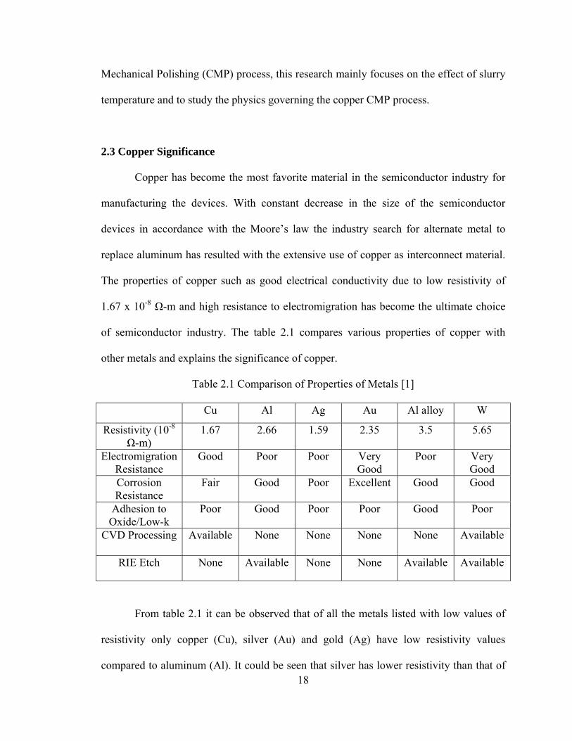
2.3 Copper Significance
Copper has become the most favorite material in the semiconductor industry for
manufacturing the devices. With constant decrease in the size of the semiconductor
devices in accordance with the Moore’s law the industry search for alternate metal to
replace aluminum has resulted with the extensive use of copper as interconnect material.
The properties of copper such as good electrical conductivity due to low resistivity of
1.67 x 10⁻⁸ Ω-m and high resistance to electromigration has become the ultimate choice
of semiconductor industry. The table 2.1 compares various properties of copper with
other metals and explains the significance of copper.
Table 2.1 Comparison of Properties of Metals [1]
Cu Al Ag Au Al alloy W
Resistivity (10-8 Ω-m)
1.67 2.66 1.59 2.35 3.5 5.65
Electromigration Resistance
Good Poor Poor Very Good
Poor Very Good
Corrosion Resistance
Fair Good Poor Excellent Good Good
Adhesion to Oxide/Low-k
Poor Good Poor Poor Good Poor
CVD Processing Available None None None None Available
RIE Etch None Available None None Available Available
From table 2.1 it can be observed that of all the metals listed with low values of
resistivity only copper (Cu), silver (Au) and gold (Ag) have low resistivity values
compared to aluminum (Al). It could be seen that silver has lower resistivity than that of
19
copper, but silver diffuses easily into silicon dioxide (SiO2) and also has poor resistance
to electromigration. Whereas copper has good electromigration resistance and search for
proper barrier layers to prevent Ag diffusion into oxide couldn’t yield any success. Gold
(Au) has high resistance to corrosion and electromigration but has higher resistivity
compared to copper. Also copper has high melting and boiling points (1357.77, 2835 K)
compared to silver (1235, 2435 K) and aluminum (933.5, 2792 K) [33]. Current densities
in the lower interconnect levels can lead to electromigration failure. Copper can carry
higher current densities compared to aluminum and its alloys and has high
electromigration resistance [34].
Copper with all the above properties compared to other available low resistivity
metals make it an inevitable choice as a interconnect metal. Even though copper has good
properties to be a interconnect metal it has its own drawback and is not without
challenges. Copper low adhesion and diffuses easily into oxide/low-k. However
researchers have come up with various barrier metals such as tantalum (Ta), tantalum
nitride (TaN), titanium (Ti), titanium dioxide (TiO2) etc., to improve copper adhesion
and avoid diffusion into oxide. Copper also is not resistant to corrosion and hence a
passivation layer is required. Researchers were successful in finding methods for
passivating copper to avoid corrosion [1]. Of all these the major challenge for use of
copper as a interconnect metal is copper cannot be etched or patterned using the available
wet/dry etch techniques. With the introduction of Chemical Mechanical Polishing (CMP)
the problem of patterning copper could be eliminated and copper has found a widespread
use in semiconductor industry as a interconnect metal.
20
2.4 Copper Deposition Techniques
Copper films can be deposited in a number of ways, such as chemical vapor
deposition (CVD), physical vapor deposition (PVD), electroplating and electroless
plating.
2.4.1 Chemical Vapor Deposition (CVD)
The CVD process uses precursors for copper deposition and organo-mettalic
sources are the most commonly used precursors for CVD of copper. Precursors such as
copper (II) hexa-fluoro-acetyl-acetonate [CuII(hfac)2] and CuI(hfac)L, where L is a
weakly bonded neutral ligand are used. Copper films of higher quality can be obtained by
hydrogen reduction of CuII(hfac)2. In order to obtain copper films with low resistivity the
deposition temperature must be in the range of 350-450 °C, but since use of copper with
low-k dielectric materials which are thermally fragile such high deposition temperatures
are undesirable. Various deposition process have been developed of which a low-pressure
plasma process has been reported which allows for copper deposition at 170 °C and films
with comparatively low resistivity can be obtained. Chemical vapor deposition process
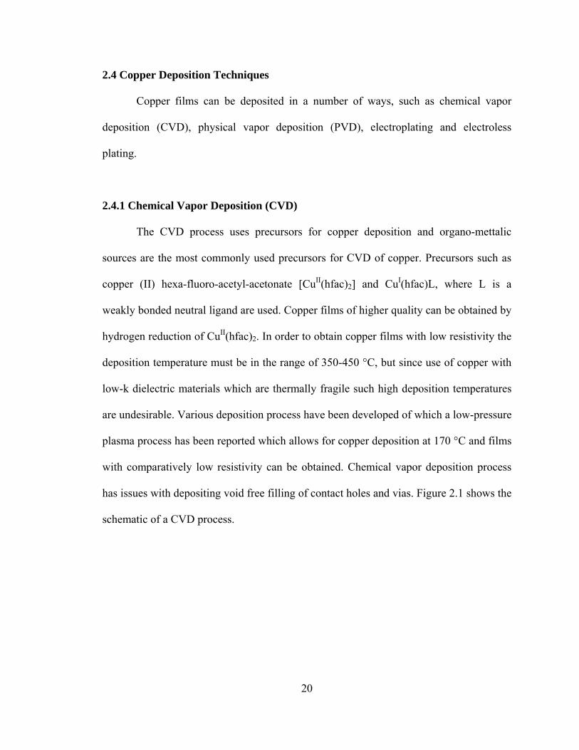
has issues with depositing void free filling of contact holes and vias. Figure 2.1 shows the
schematic of a CVD process.
21
Figure 2.1 Schematic of a CVD Process [35]
2.4.2 Physical Vapor Deposition (PVD)
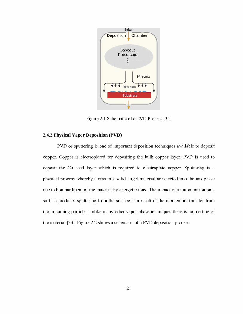
PVD or sputtering is one of important deposition techniques available to deposit
copper. Copper is electroplated for depositing the bulk copper layer. PVD is used to
deposit the Cu seed layer which is required to electroplate copper. Sputtering is a
physical process whereby atoms in a solid target material are ejected into the gas phase
due to bombardment of the material by energetic ions. The impact of an atom or ion on a
surface produces sputtering from the surface as a result of the momentum transfer from
the in-coming particle. Unlike many other vapor phase techniques there is no melting of
the material [33]. Figure 2.2 shows a schematic of a PVD deposition process.
Inlet Deposition Chamber
Plasma
Gaseous Precursors
22
Figure 2.2 Schematic of a PVD Process [33]
2.4.3 Copper Electroplating
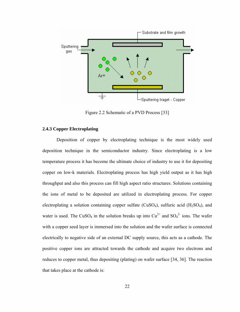
Deposition of copper by electroplating technique is the most widely used
deposition technique in the semiconductor industry. Since electroplating is a low
temperature process it has become the ultimate choice of industry to use it for depositing
copper on low-k materials. Electroplating process has high yield output as it has high
throughput and also this process can fill high aspect ratio structures. Solutions containing
the ions of metal to be deposited are utilized in electroplating process. For copper
electroplating a solution containing copper sulfate (CuSO4), sulfuric acid (H2SO4), and
water is used. The CuSO4 in the solution breaks up into Cu2+ and SO42- ions. The wafer
with a copper seed layer is immersed into the solution and the wafer surface is connected
electrically to negative side of an external DC supply source, this acts as a cathode. The
positive copper ions are attracted towards the cathode and acquire two electrons and
reduces to copper metal, thus depositing (plating) on wafer surface [34, 36]. The reaction
that takes place at the cathode is:
23
Cu2+ + 2e- Cu (2.1)
The anode is attached to the positive side of the external DC supply source. The
rate of electroplating is a direct function of current density. Electroplating process has
very high deposition rates. Figure 2.3 shows the schematic of copper electroplating
system.
Figure 2.3 Schematic of a Copper Electroplating System [37]
2.4.4 Electroless-Plating
The process of copper deposition through electroless-plating involves the
formation of a thin film from an electrolytic solution without externally applied voltage
as in case of electroplating. In the electroless process the deposition takes place due to
electrochemical reaction between the metal ions, complexing, reducing agent, and pH
buffers on catalytic surfaces. The chemical process involves CuO4 and formaldehyde
reduction: [34, 38]
Cu2+ +2HCHO + 4OH- Cuo (solid) + 2H2O (liquid) + H2 (gas) (2.2)
24
The main challenge in using both electroplating and electroless-plating is to
obtain a void free surface.
2.5 Copper Removal Mechanism
Each material has different removal mechanisms as different materials being
polished have different hardnesses and removal chemistry. The chemical mechanical
polishing (CMP) of copper several differences compared to CMP of oxide/low-k, barrier
metals and tungsten. Copper with a hardness of ~ 3 GPa [33] is softer in nature and is
easily abraded compared to other materials. The removal of copper basically takes place
in about three steps viz., 1) chemical reaction of slurry with copper to form surface layer.
2) Followed by mechanical abrasion of copper surface by abrasives present in slurry. 3)
Removal of the abraded copper material from the copper surface. The abraded particles
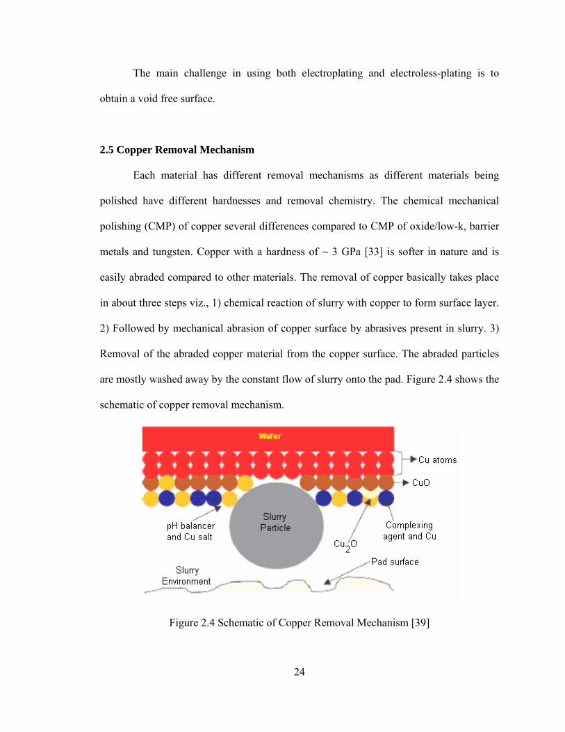
are mostly washed away by the constant flow of slurry onto the pad. Figure 2.4 shows the
schematic of copper removal mechanism.
Figure 2.4 Schematic of Copper Removal Mechanism [39]
25
2.5.1 Formation of Surface Layer
Initially when the wafer surface comes into contact with slurry film it forms a
native oxide, hydroxide films, Cu2O, CuO and Cu(OH)2 surface layer depending upon the
slurry being used. Film growth on the surfaces being abraded is controlled by both
growth kinetics as well as abrasion dynamics. Copper CMP is generally performed using
basic and acidic slurries. Removal rate of copper is low in basic slurries compared to
acidic slurries.
Basic slurries usually consist of ammonium hydroxide (NH4OH), 1 vol% NH4OH
[1]. While using basic slurries a Cu2O surface layer is formed. The removal rate is low in
ammonium hydroxide based slurries. Even though high solubility of copper in ammonia
based slurries the low removal rate is due to the formation of Cu2O layer on the surface.
The surface layer acts as a barrier to etching and slows the dissolution of copper.
Acidic slurries usually consist of nitric acid (HNO3). The acidic slurries generally
have low pH values and at low pH values copper doesn’t form a surface layer. Studies
have shown that as HNO3 concentration increases the etch rate also increases linearly.
This suggests that there no formation of a surface layer. The disadvantage of using acidic
slurries is that the high etch rate results in a high removal rate in the recessed areas. The
surface is susceptant to corrosion in acidic slurries. In order to avoid corrosion during
polishing with acidic slurries a corrosion inhibitor such as benzotriazole (BTA) is added
[40]. With addition of BTA a monolayer of Cu-BTA is formed which protects the surface
from corrosion.
26
Due to the corrosive nature of the acidic slurries surface defects such as dishing
might take place in the recessed areas. The NH4OH based does not etch copper and
therefore dishing might be only due to the pad reaching into the recessed region.
2.5.2 Abrasion
The abrasive component, whether delivered in a solution phase or abraded form a
solid phase, generally provides the mechanical part of CMP. The abrasive particle
impacts the surface and abrades the chemically treated surface exposing new material for
chemical attack [41]. The particles are either colloidal or non-colloidal in nature. The
most commonly used abrasive particles are fumed, colloidal silica, aluminum oxide
(Al2O3), ceria etc., Copper CMP does not require chemical activity from the particle. In
general the size of abrasive particles may vary between 25 nm – 1 micron in diameter.
2.5.3 Removal of Abraded Material
Once the material is abraded from the copper surface the abraded material must
be removed from the vicinity of the surface so that it does not redeposit. Since the pad
makes constant rotation the chance of the abraded material returning back to surface is
high. There have been several ways by which abraded material can be removed. The best
method is by passing a constant flow of slurry, due the turbulent motion of the slurry the
abraded material is washed away with constant inflow of new slurry. Also different
oxidizing agents could be used with basic and acidic slurries so that the copper polish rate
may be increased by increasing the dissolution rate of abraded material. This primarily
27
serves two purposes by increasing the removal rate and by removing the abraded material
[1].
2.6 Pattern Geometry Effects on Removal Mechanism
Copper dishing and ILD erosion are the two main undesired defects in CMP
process. The dishing and erosion occur during the over polish step which is required to
ensure complete copper removal across the entire wafer. The copper dishing can be
defined as the difference in height between the center of the copper line, which is the
lowest point of the dish, and the point where ILD levels off. Dishing in copper mainly
occurs due to bending of polishing pad slightly into the recess to remove the copper from
within the recess. Dielectric erosion is a thinning of dielectric layer, resulting because of
the reason that the polish rate of oxide is non-zero during the over polish time. The
dishing leads to reduction in final thickness of copper line and resulting in complications
while adding multiple layers of metal [1] the dishing increases with increase in metal line
width.
2.7 Defects During CMP
The chemical mechanical planarization process with many advantages also has
some disadvantages in the form of surface defects caused during the planarization
process. These defects cause complications while adding multiple layers of metal and
other dielectric layers. Figure 2.5 shows some of the defects formed during metal CMP.
The various defects formed during CMP are listed below:
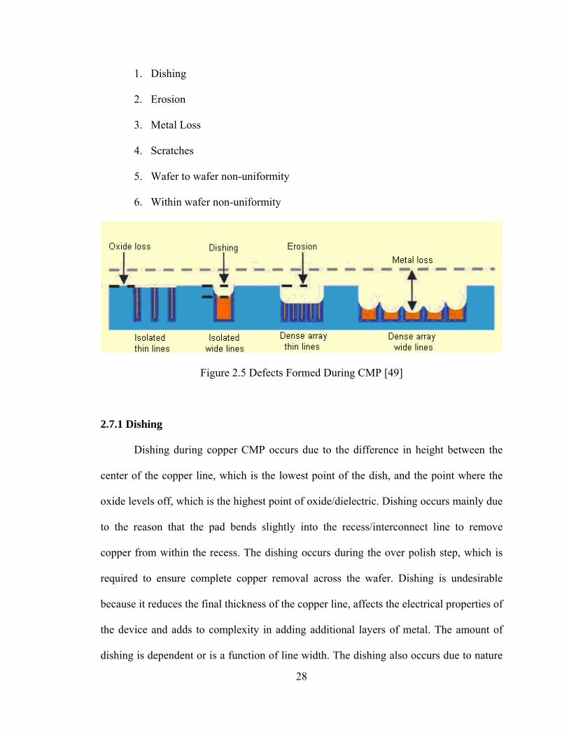
28
1. Dishing
2. Erosion
3. Metal Loss
4. Scratches
5. Wafer to wafer non-uniformity
6. Within wafer non-uniformity
Figure 2.5 Defects Formed During CMP [49]
2.7.1 Dishing
Dishing during copper CMP occurs due to the difference in height between the
center of the copper line, which is the lowest point of the dish, and the point where the
oxide levels off, which is the highest point of oxide/dielectric. Dishing occurs mainly due
to the reason that the pad bends slightly into the recess/interconnect line to remove
copper from within the recess. The dishing occurs during the over polish step, which is
required to ensure complete copper removal across the wafer. Dishing is undesirable
because it reduces the final thickness of the copper line, affects the electrical properties of
the device and adds to complexity in adding additional layers of metal. The amount of
dishing is dependent or is a function of line width. The dishing also occurs due to nature

29
of pad physical and mechanical properties. Rigid pads are founds to cause less amount of
dishing on patterned wafers. The removal rate of the metal is lower inside the recess
because the pad does not exert the same pressure on the recessed surface as on the flat
metal surface [1]. The dishing can be reduced by controlling the over polish time closely.
Figure 2.6 shows the schematic of copper dishing.
Figure 2.6 Schematic of Copper Dishing During CMP [49]
2.7.2 Erosion
Erosion is the thinning of oxide/dielectric layer caused due to the difference in
polish rate between copper and oxide/dielectric during the over polish step. It can be said
as the difference in thickness before and after polishing. Oxide erosion is dependent on
the pattern density of the features under polish. The removal rate of oxide increases with
increase in copper pattern density. This is due to the reason that as the copper pattern
density increases there is lesser amount of oxide available to support the force and
increase in oxide removal rate. With increase in pattern density tends to cause an increase
in pressure on oxide thus increasing the oxide polish rate. Erosion during polishing is
undesirable as it degrades the electrical properties of the device and increases the process
complexity while adding more layers over it and finally may short the device electrically.
30
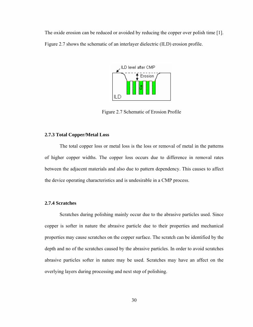
The oxide erosion can be reduced or avoided by reducing the copper over polish time [1].
Figure 2.7 shows the schematic of an interlayer dielectric (ILD) erosion profile.
Figure 2.7 Schematic of Erosion Profile
2.7.3 Total Copper/Metal Loss
The total copper loss or metal loss is the loss or removal of metal in the patterns
of higher copper widths. The copper loss occurs due to difference in removal rates
between the adjacent materials and also due to pattern dependency. This causes to affect
the device operating characteristics and is undesirable in a CMP process.
2.7.4 Scratches
Scratches during polishing mainly occur due to the abrasive particles used. Since
copper is softer in nature the abrasive particle due to their properties and mechanical
properties may cause scratches on the copper surface. The scratch can be identified by the
depth and no of the scratches caused by the abrasive particles. In order to avoid scratches
abrasive particles softer in nature may be used. Scratches may have an affect on the
overlying layers during processing and next step of polishing.

31
2.7.5 Wafer to Wafer Non-uniformity
Wafer to wafer non-uniformity (WTWNU) is the difference in the amount of the
polishing observed between wafer to wafer. This may be caused due to various process
parameters controllable and uncontrollable. The WTWNU is caused due to decay in
material removal rate with polishing more number of wafers on the same pad for a longer
time [50]. This may also due to the change in wafer surface properties.
2.7.6 Within Wafer Non-uniformity
The within wafer non-uniformity (WIWNU) is due to the variation in material
removal rate in CMP process. It has been observed that even with a uniform down force
the material removal rate is not uniform across the wafer [50]. The non-uniformity in
polishing may be caused due to degrading pad polishing properties or may be due to non-
uniformity in the applied down force across the wafer surface.
2.8 Summary
With shrinking device dimensions and increasing RC delay there has been an
extensive search for various new metals to replace aluminum as a interconnect material.
Various materials as potential replacements were considered but copper a good electrical
conductor with low resistivity, high current density and high electromigration resistance
has replaced aluminum as the interconnect material. Although copper possesses all the
characteristics of a good electrical conductor it also has some disadvantages or
complications. Unlike aluminum copper cannot be etched, which was overcomed by
introduction of Chemical Mechanical Polishing (CMP) where copper is etched due to
32
interaction of chemical and mechanical components. First the surface is altered
chemically and then abraded away by the abrasive particles present in the slurry. Copper
also diffuses easily into oxide/low-k dielectrics and in order to avoid this barrier layer has
to be deposited. Copper can be deposited by various methods, such as CVD, PVD,
electroplating and electroless-plating. Copper with all characteristics of a good electrical
conductor has assumed a significant place in semiconductor manufacturing as an
interconnect material. Copper CMP with its advantages also has some problems that are
caused due to surface defects such as dishing, erosion, scratches, wafer to wafer non-
uniformity and within wafer non-uniformity. These defects can be minimized by reducing
the over polish time and by selectively choosing the polishing pads and other
consumables.
33
Chapter 3
Experimental
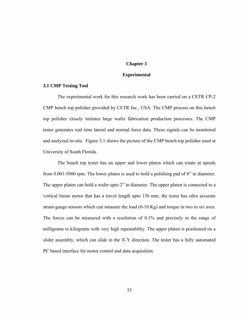
3.1 CMP Testing Tool
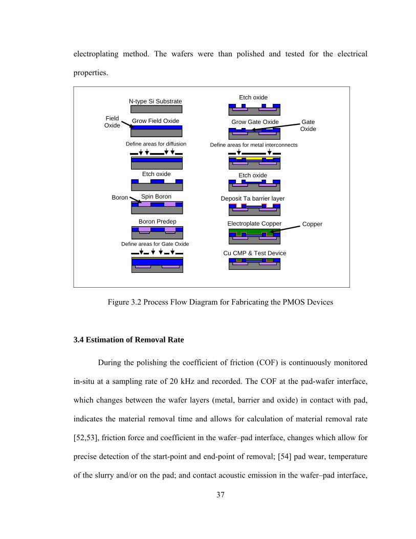
The experimental work for this research work has been carried on a CETR CP-2
CMP bench top polisher provided by CETR Inc., USA. The CMP process on this bench
top polisher closely imitates large wafer fabrication production processes. The CMP
tester generates real time lateral and normal force data. These signals can be monitored
and analyzed in-situ. Figure 3.1 shows the picture of the CMP bench top polisher used at
University of South Florida.
The bench top tester has an upper and lower platen which can rotate at speeds
from 0.001-5000 rpm. The lower platen is used to hold a polishing pad of 6” in diameter.
The upper platen can hold a wafer upto 2” in diameter. The upper platen is connected to a
vertical linear motor that has a travel length upto 150 mm. the tester has ultra accurate
strain-gauge sensors which can measure the load (0-10 Kg) and torque in two to six axes.
The forces can be measured with a resolution of 0.1% and precisely in the range of
milligrams to kilograms with very high repeatability. The upper platen is positioned on a
slider assembly, which can slide in the X-Y direction. The tester has a fully automated
PC based interface for motor control and data acquisition.

34
Figure 3.1 CMP Bench Top Tester
3.2 CMP Consumables
The experiments were carried out on 2 cm X 2 cm patterned copper wafers having
MIT 854 structure. The patterned copper samples had a barrier and low-k layers beneath
the copper. The samples were polished using two different kinds of polishing pad and
copper slurry containing colloidal silica as abrasive particles. The polishing pads used
were Pad A with SUBA IV subpad and Pad B. Subpads were used with both the
polishing pads in order to reduce the non-uniformity during polishing. Hydrogen
peroxide (H2O2) was used as the oxidizer in the slurry for polishing. The pad was
conditioned using deionized (DI) water for 10 minutes prior to polishing each sample to
Slider Assembly
AE Sensor
Slurry Flow
Force Sensor
Wafer Carrier
Polishing Pad
Slurry Outlet
35
increase the roughness of the pad. The initial thickness of copper on the unpolished
samples was 1 µm.
3.3 Experimental Parameters
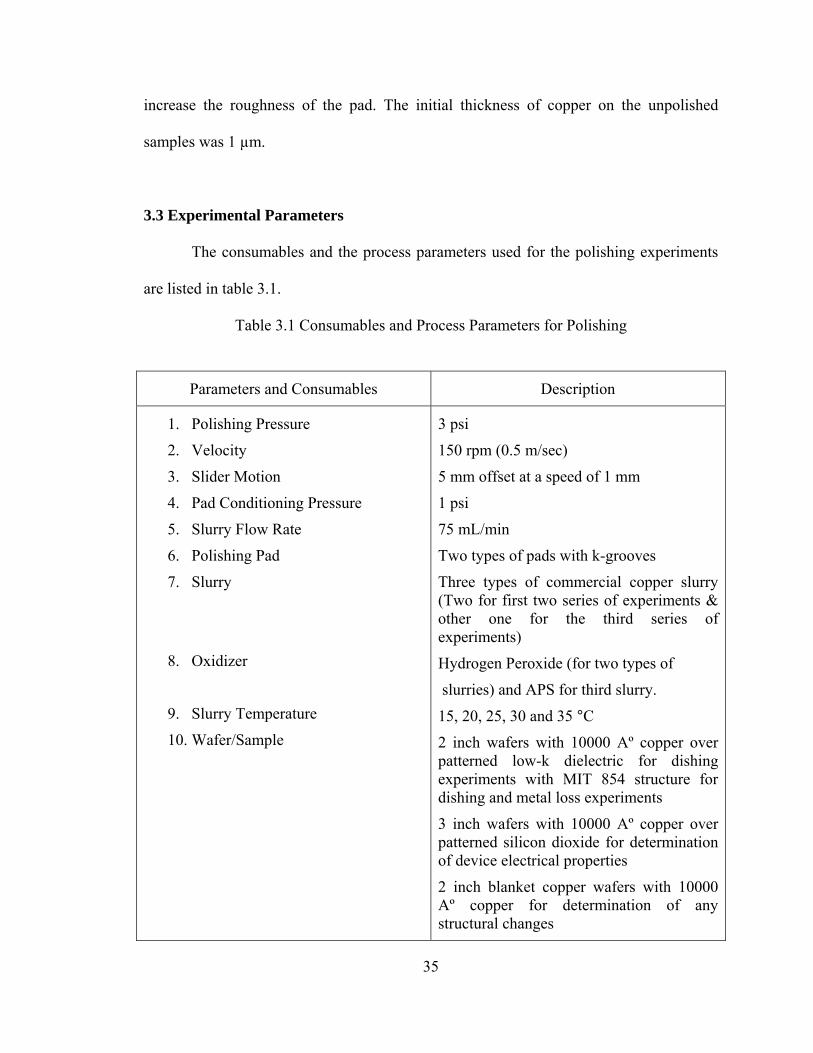
The consumables and the process parameters used for the polishing experiments
are listed in table 3.1.
Table 3.1 Consumables and Process Parameters for Polishing
Parameters and Consumables Description
1. Polishing Pressure
2. Velocity
3. Slider Motion
4. Pad Conditioning Pressure
5. Slurry Flow Rate
6. Polishing Pad
7. Slurry
8. Oxidizer
9. Slurry Temperature
10. Wafer/Sample
3 psi
150 rpm (0.5 m/sec)
5 mm offset at a speed of 1 mm
1 psi
75 mL/min
Two types of pads with k-grooves
Three types of commercial copper slurry (Two for first two series of experiments & other one for the third series of experiments)
Hydrogen Peroxide (for two types of
slurries) and APS for third slurry.
15, 20, 25, 30 and 35 °C
2 inch wafers with 10000 Aº copper over patterned low-k dielectric for dishing experiments with MIT 854 structure for dishing and metal loss experiments
3 inch wafers with 10000 Aº copper over patterned silicon dioxide for determination of device electrical properties
2 inch blanket copper wafers with 10000 Aº copper for determination of any structural changes
36
The patterned copper samples were 2 inch wafers with MIT 854 structure and
were polished using two different pads, pad A and pad B with subpads. The pad A has
perforations in it and pad B polishing pad has k-grooves in it. Pad B is softer in nature
compared to pad A. The pads were conditioned for 10 minutes prior to polishing each
sample to ensure that the pad roughness remained constant throughout the polishing
process. The pressure and platen velocity were maintained constantly at 3psi and 150 rpm
through out the polishing. The slider was allowed to oscillate 5mm in X-Y direction at a
velocity of 1mm/sec. The slurry temperature was varied at 15 °C, 20 °C, 25 °C, 30 °C
and 35 °C. The slurry temperature was controlled for each experiment during the whole
project by monitoring and maintaining the temperature at a specific value within a 0.2 oC
variation using a temperature controller.
Temperatures below and above room temperature were investigated as there is a
very minimal probability of slurry temperature going down very low or very high; also as
heat is generated during polishing to rubbing of two surfaces there is a raise in
temperature. As recommended by the manufacturer the temperatures above 40 °C were
avoided as the slurry would undergo changes chemically and would be rendered useless.
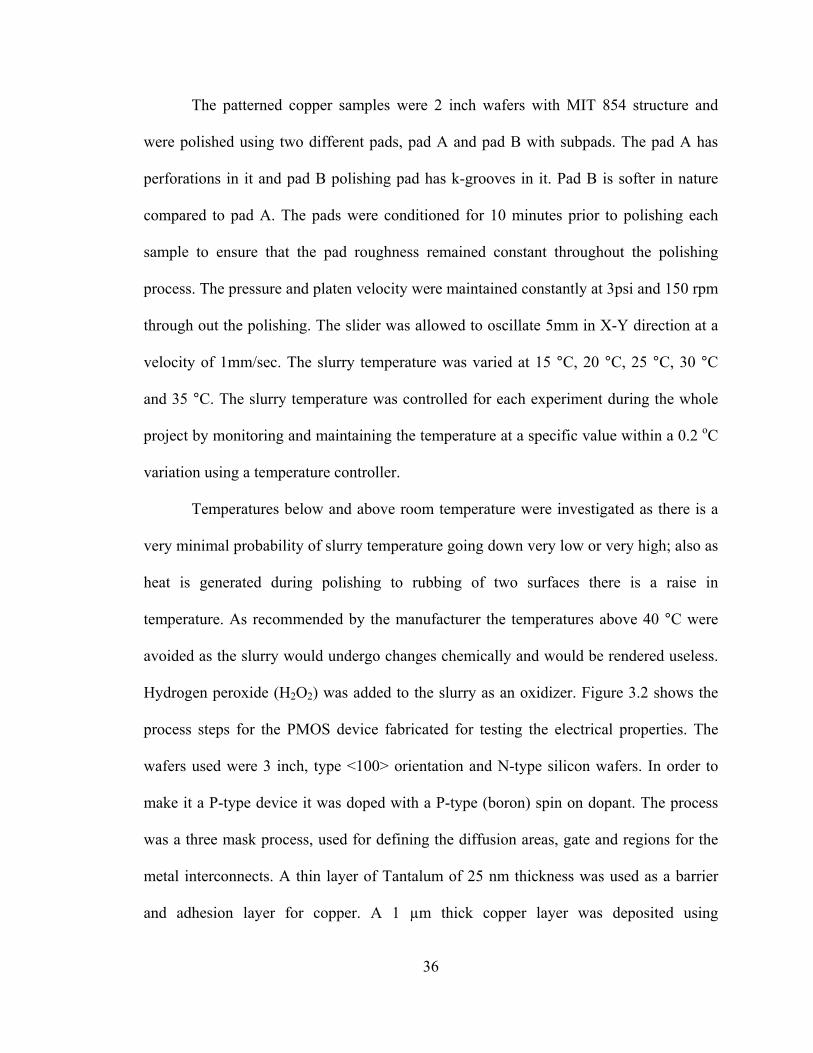
Hydrogen peroxide (H2O2) was added to the slurry as an oxidizer. Figure 3.2 shows the
process steps for the PMOS device fabricated for testing the electrical properties. The
wafers used were 3 inch, type <100> orientation and N-type silicon wafers. In order to
make it a P-type device it was doped with a P-type (boron) spin on dopant. The process
was a three mask process, used for defining the diffusion areas, gate and regions for the
metal interconnects. A thin layer of Tantalum of 25 nm thickness was used as a barrier
and adhesion layer for copper. A 1 µm thick copper layer was deposited using
37
electroplating method. The wafers were than polished and tested for the electrical
properties.
Figure 3.2 Process Flow Diagram for Fabricating the PMOS Devices
3.4 Estimation of Removal Rate
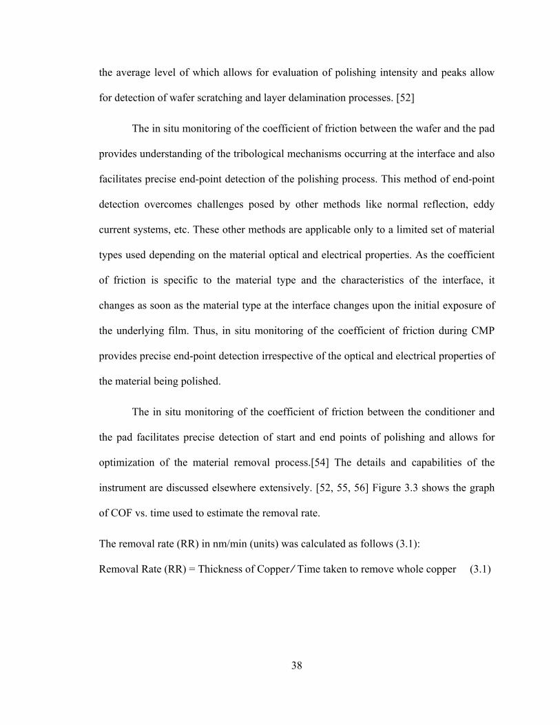
During the polishing the coefficient of friction (COF) is continuously monitored
in-situ at a sampling rate of 20 kHz and recorded. The COF at the pad-wafer interface,
which changes between the wafer layers (metal, barrier and oxide) in contact with pad,
indicates the material removal time and allows for calculation of material removal rate
[52,53], friction force and coefficient in the wafer–pad interface, changes which allow for
precise detection of the start-point and end-point of removal; [54] pad wear, temperature
of the slurry and/or on the pad; and contact acoustic emission in the wafer–pad interface,
N-type Si Substrate
Grow Field Oxide
Define areas for diffusion
Etch oxide
Spin Boron
Boron Predep
Define areas for Gate Oxide
Etch oxide
Grow Gate Oxide
Define areas for metal interconnects
Etch oxide
Deposit Ta barrier layer
Electroplate Copper
Cu CMP & Test Device
Field Oxide
Boron
Gate Oxide
Copper
38
the average level of which allows for evaluation of polishing intensity and peaks allow
for detection of wafer scratching and layer delamination processes. [52]
The in situ monitoring of the coefficient of friction between the wafer and the pad
provides understanding of the tribological mechanisms occurring at the interface and also
facilitates precise end-point detection of the polishing process. This method of end-point
detection overcomes challenges posed by other methods like normal reflection, eddy
current systems, etc. These other methods are applicable only to a limited set of material
types used depending on the material optical and electrical properties. As the coefficient
of friction is specific to the material type and the characteristics of the interface, it
changes as soon as the material type at the interface changes upon the initial exposure of
the underlying film. Thus, in situ monitoring of the coefficient of friction during CMP
provides precise end-point detection irrespective of the optical and electrical properties of
the material being polished.
The in situ monitoring of the coefficient of friction between the conditioner and
the pad facilitates precise detection of start and end points of polishing and allows for
optimization of the material removal process.[54] The details and capabilities of the
instrument are discussed elsewhere extensively. [52, 55, 56] Figure 3.3 shows the graph
of COF vs. time used to estimate the removal rate.
The removal rate (RR) in nm/min (units) was calculated as follows (3.1):
Removal Rate (RR) = Thickness of Copper ⁄ Time taken to remove whole copper (3.1)
39
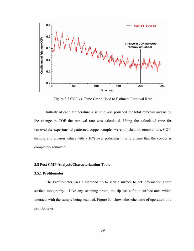
Figure 3.3 COF vs. Time Graph Used to Estimate Removal Rate
Initially at each temperature a sample was polished for total removal and using
the change in COF the removal rate was calculated. Using the calculated time for
removal the experimental patterned copper samples were polished for removal rate, COF,
dishing and erosion values with a 10% over polishing time to ensure that the copper is
completely removed.
3.5 Post CMP Analysis/Characterization Tools
3.5.1 Profilometer
The Profilometer uses a diamond tip to scan a surface to get information about
surface topography. Like any scanning probe, the tip has a finite surface area which
interacts with the sample being scanned. Figure 3.4 shows the schematic of operation of a
profilometer.

40
Figure 3.4 Schematic of a Profilometer Scan
The tip scans across the surface of the sample, and an inductive sensor registers
the vertical motion of the tip. The signal generated by the motion of the tip is used to
create a two-dimensional profile of the surface from which the step height can be
calculated [42].
3.5.2 Atomic Force Microscopy (AFM)
The atomic force microscopy (AFM) works similar to the same way as a
profilometer works, only on a much, much smaller scale. The AFM consists of a
microscale cantilever with a sharp tip (probe) at its end that is used to scan the specimen
surface. The cantilever is typically made of silicon or silicon nitride with a tip radius of
curvature on the order of about 10 nanometers. When the tip is brought into proximity of
a sample surface, forces between the tip and the sample lead to a deflection of the
cantilever according to Hooke's law. The change in the vertical position (due to repulsive
or attractive Van der Waals force) reflects the topography of the surface. By collecting
the height data for a succession of lines it is possible to form a three dimensional map of

41
the surface features. A tip or cantilever which drags across the surface of the sample is
specially constructed for surface structure investigation. Figure 3.5 shows the schematic
of an AFM and figure 3.6 shows the SEM picture/schematic of an AFM cantilever/tip
[33, 42].
Figure 3.5 Schematic of Operation of an AFM [33]
Figure 3.6 SEM Image/Schematic of an AFM Cantilever Tip [42]

42
3.5.3 Scanning Electron Microscopy (SEM)
The scanning electron microscope (SEM) is used to produce high resolution
images of high magnification upto atomic level. In a SEM electrons are thermionically
emitted from tungsten which acts as a cathode and are accelerated towards an anode;
alternatively electrons can be emitted via field emission (FE). The electron beam, which
typically has an energy ranging from a few 100 eV to 50 keV, is focused by one or two
condenser lenses into a beam with a very fine focal spot sized in the order of 1 nm to 5
nm. The electron beam then passes through a pair of scanning coils in the objective lens,
which deflect the beam in a raster fashion over a rectangular area of the sample surface.
As the primary electrons strike the surface they are inelastically scattered by atoms in the
sample. Through these scattering events, the primary electron beam effectively spreads
and fills a teardrop-shaped volume, known as the interaction volume, extending from less
than 100 nm to around 5 µm into the surface. Interactions in this region lead to the
subsequent emission of electrons which are then detected to produce an image [33].
Figure 3.7 shows the basic block diagram of a scanning electron microscope.
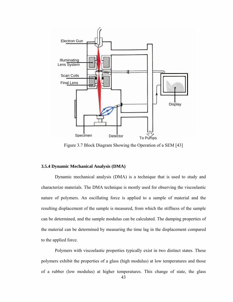
43
Figure 3.7 Block Diagram Showing the Operation of a SEM [43]
3.5.4 Dynamic Mechanical Analysis (DMA)
Dynamic mechanical analysis (DMA) is a technique that is used to study and
characterize materials. The DMA technique is mostly used for observing the viscoelastic
nature of polymers. An oscillating force is applied to a sample of material and the
resulting displacement of the sample is measured, from which the stiffness of the sample
can be determined, and the sample modulus can be calculated. The damping properties of
the material can be determined by measuring the time lag in the displacement compared
to the applied force.
Polymers with viscoelastic properties typically exist in two distinct states. These
polymers exhibit the properties of a glass (high modulus) at low temperatures and those
of a rubber (low modulus) at higher temperatures. This change of state, the glass
Electron Gun
Illuminating Lens System
Scan Coils
Final Lens
Display
To Pumps Specimen Detector
44
transition or alpha relaxation, can be observed during DMA run by scanning the
temperature. The DMA technique is most widely used to investigate viscoelastic
properties of CMP polishing pads as it can yield better data and can also be used to
investigate the frequency dependant nature of the glass transition [33]. The DMA
operation of DMA is based on the equation 3.2 [44]:
G* = G’ + iG” (3.2)
Where G* is the complex modulus, G” is loss modulus, i is imaginary root of -1
and G’ is storage modulus. Storage modulus (G’) gives the elastic properties of the
material and is measured directly. The loss modulus factor (iG”) gives the details about
the viscous properties of the material. The ratio of loss modulus to storage modulus gives
the tan delta or the damping ratio [45].
The DMA were performed using a DMA 2980 in the single cantilever bending
mode. The pad samples were fixed using the DMA fixture clamps. The polyurethane pad
samples with dimensions of 21.93x5.2x1.32 mm (pad A) and 21.83x5.75x1.37 mm (pad
B) were tested using a multi frequency deformation mode at frequencies ranging from 1 –
100 Hz. The temperature was increased at a rate of 5 ºC/min and was tested from -150 ºC
to 100 ºC. The samples were tested in the tension mode and liquid nitrogen was used for
sub-ambient testing. Generally, in a DMA test storage modulus (G’), loss modulus (G”)
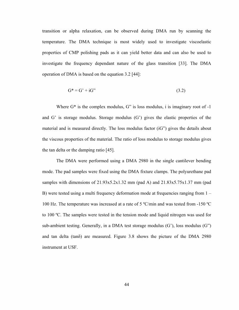
and tan delta (tanδ) are measured. Figure 3.8 shows the picture of the DMA 2980
instrument at USF.
45
Figure 3.8 DMA 2980 Instrument at USF [48]
3.5.5 X-Ray Diffraction (XRD)
X-rays are electromagnetic radiation similar to light, but with a much shorter
wavelength. They are produced when electrically charged particles of sufficient energy
are decelerated. Typically in an X-ray tube, the high voltage maintained across the
electrodes draws electrons toward a metal target. X-rays are produced at the point of
impact, and radiate in all directions. [42]
If an incident X-ray beam encounters a crystal lattice, general scattering occurs.
Although most scattering interferes with itself and is eliminated, diffraction occurs when
scattering in a certain direction is in phase with scattered rays from other atomic planes.
Under this condition the reflections combine to form new enhanced wave fronts that
mutually reinforce each other. The relation by which diffraction occurs is known as the
46
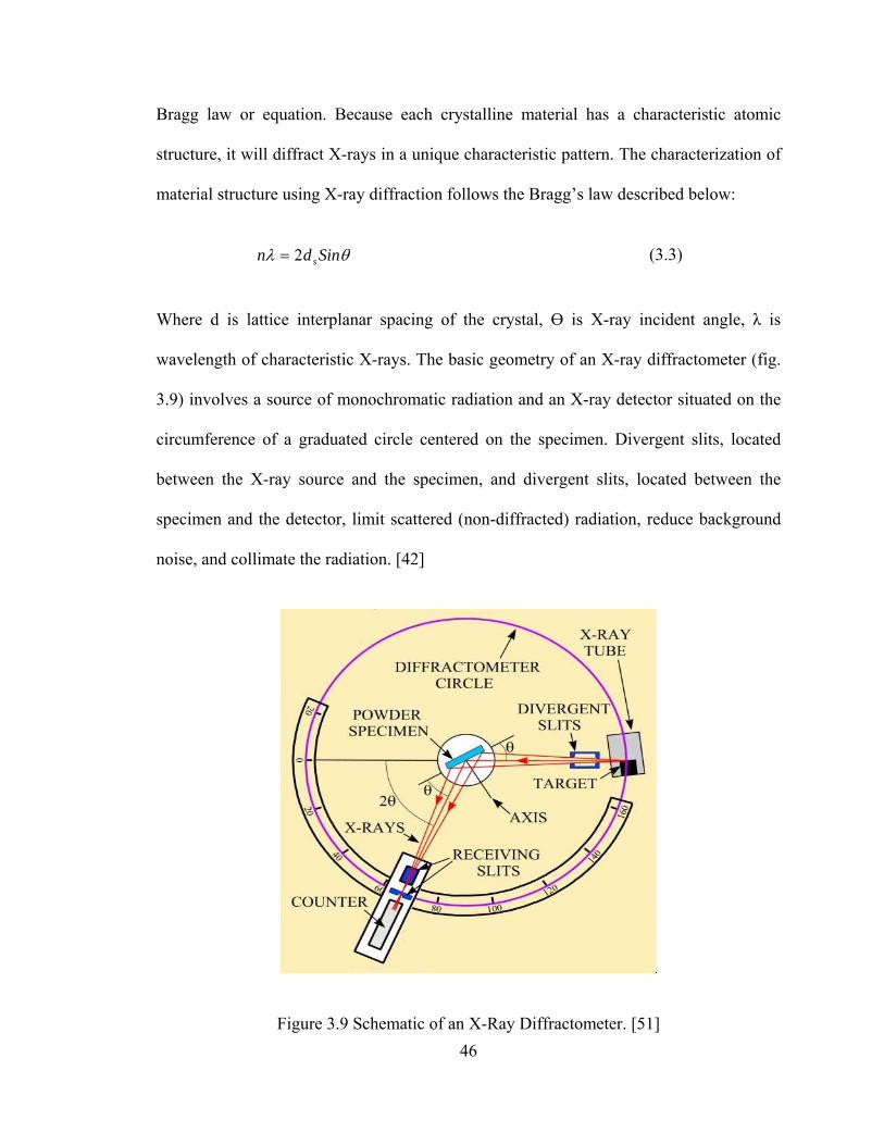
Bragg law or equation. Because each crystalline material has a characteristic atomic
structure, it will diffract X-rays in a unique characteristic pattern. The characterization of
material structure using X-ray diffraction follows the Bragg’s law described below:
θλ Sindn s2= (3.3)
Where d is lattice interplanar spacing of the crystal, Ө is X-ray incident angle, λ is
wavelength of characteristic X-rays. The basic geometry of an X-ray diffractometer (fig.
3.9) involves a source of monochromatic radiation and an X-ray detector situated on the
circumference of a graduated circle centered on the specimen. Divergent slits, located
between the X-ray source and the specimen, and divergent slits, located between the
specimen and the detector, limit scattered (non-diffracted) radiation, reduce background
noise, and collimate the radiation. [42]
Figure 3.9 Schematic of an X-Ray Diffractometer. [51]
47
The detector and specimen holder are mechanically coupled with a goniometer so
that a rotation of the detector through 2x degrees occurs in conjunction with the rotation
of the specimen through x degrees, a fixed 2:1 ratio. A curved-crystal monochromator
containing a graphite crystal is normally used to ensure that the detected radiation is
monochromatic. When positioned properly just in front of the detector, only the K
radiation is directed into the detector, and the Kß radiation, because it is diffracted at a
slightly different angle, is directed away.
3.6 Summary
The CMP tool used for the experiments closely imitates large wafer fabrication
production processes. The CMP tester generates real time lateral and normal force data.
These signals can be monitored and analyzed in-situ. The polishing experiments were
carried on CETR Cp-2 bench top polisher. The patterned copper samples were polished at
different slurry temperatures keeping the pressure and velocity throughout the
experiments. Two different kinds of pads and one type of polishing slurry were used for
polishing experiments. The patterned copper samples polished at different condition were
analyzed for the amount of dishing and erosion using atomic force microscopy (AFM)
and profilometer. The change in pad physical properties with increase in temperature was
analyzed using dynamic mechanical analysis (DMA). The surface morphology of the pad
before and after conditioning was analyzed using scanning electron microscopy (SEM).
The pad roughness before and after conditioning was measured using the profilometer.
The structural changes in the copper blanket films was analyzed using X-Ray diffraction
(XRD) analysis method for any change in crystallinity after polishing at different
temperatures.

48
Chapter 4
Results and Discussion
The values of coefficient of friction COF and removal rates at different slurry
temperatures were monitored and analyzed in-situ. The removal rate was calculated using
the change in coefficient of friction (COF). The amount of dishing and metal loss during
polishing was analyzed using profilometer and atomic force microscope (AFM). The
change in pad physical properties with change in temperature was analyzed using
dynamic mechanical analysis (DMA) technique.
4.1 Dynamic Mechanical Analysis (DMA) of Pads
The CMP polishing pad is subjected to high temperatures due to friction as a
result of interaction between the polishing pad and wafer surface. This rise in temperature
is partially brought down due to slurry flow. Tregub et al had investigated the effect of
rise in temperature due to friction. The studies showed that there is a temperature rise in
the order of about 20 °C to 30 °C during CMP [46]. During the polishing process the
local pad temperature can increase significantly, especially at the point of contacts
between the trench edges and pad. The substantial increase in the pad temperature during
the CMP process can change the physical and mechanical properties of the pad.
The pads used for this research were analyzed using DMA in a frequency range of
1 to 100 Hz. Figure 4.1 shows the storage modulus and tan delta of the two polishing
pads at different temperatures. It could be seen that in the temperature range between 15
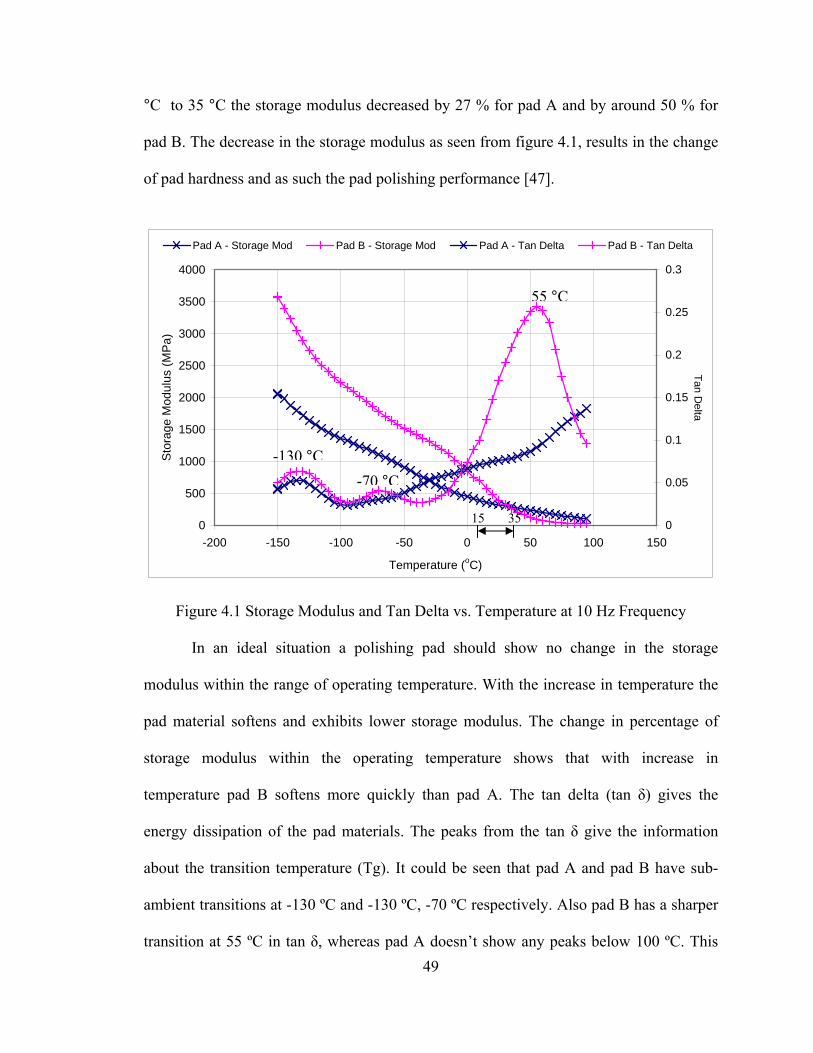
49
°C to 35 °C the storage modulus decreased by 27 % for pad A and by around 50 % for
pad B. The decrease in the storage modulus as seen from figure 4.1, results in the change
of pad hardness and as such the pad polishing performance [47].
0
500
1000
1500
2000
2500
3000
3500
4000
-200 -150 -100 -50 0 50 100 150
Temperature (oC)
Sto
rage
Mod
ulus
(MP
a)
0
0.05
0.1
0.15
0.2
0.25
0.3
Tan Delta
Pad A - Storage Mod Pad B - Storage Mod Pad A - Tan Delta Pad B - Tan Delta
Figure 4.1 Storage Modulus and Tan Delta vs. Temperature at 10 Hz Frequency
In an ideal situation a polishing pad should show no change in the storage
modulus within the range of operating temperature. With the increase in temperature the
pad material softens and exhibits lower storage modulus. The change in percentage of
storage modulus within the operating temperature shows that with increase in
temperature pad B softens more quickly than pad A. The tan delta (tan δ) gives the
energy dissipation of the pad materials. The peaks from the tan δ give the information
about the transition temperature (Tg). It could be seen that pad A and pad B have sub-
ambient transitions at -130 ºC and -130 ºC, -70 ºC respectively. Also pad B has a sharper
transition at 55 ºC in tan δ, whereas pad A doesn’t show any peaks below 100 ºC. This
55 °C
-70 °C-130 °C
15 35

50
sharp peak represents the glass transition temperature (Tg). The glass transition
temperature represents a major transition, such as change in physical properties
drastically as the material goes from hard glassy to a rubbery state. It could be interpreted
that as the temperature increases pad B loses its physical properties drastically as
compared to pad A. Thus, it could be stated that with in increase in temperature over the
operating range pad B becomes softer than pad A, loses its stiffness.
The area under the tan δ gives the ability of the pad to absorb the mechanical
energy or its toughness. Figure 4.2 shows the change in loss modulus with change in
temperature. The loss modulus (G”) is the product of the storage modulus (G’) and tan δ.
0
50
100
150
200
250
-200 -150 -100 -50 0 50 100 150
Temperature (oC)
Loss
Mod
ulus
(MPa
)
Pad A Pad B
Figure 4.2 Loss Modulus vs. Temperature at 10 Hz Frequency
4.2 Scanning Electron Microscopy (SEM) Analysis
The scanning electron microscopy (SEM) analysis was performed on both kinds
of polishing pads, before and after condition for same amount of time. The SEM analysis
gives the surface topography of the pad, which improves after the conditioning. The
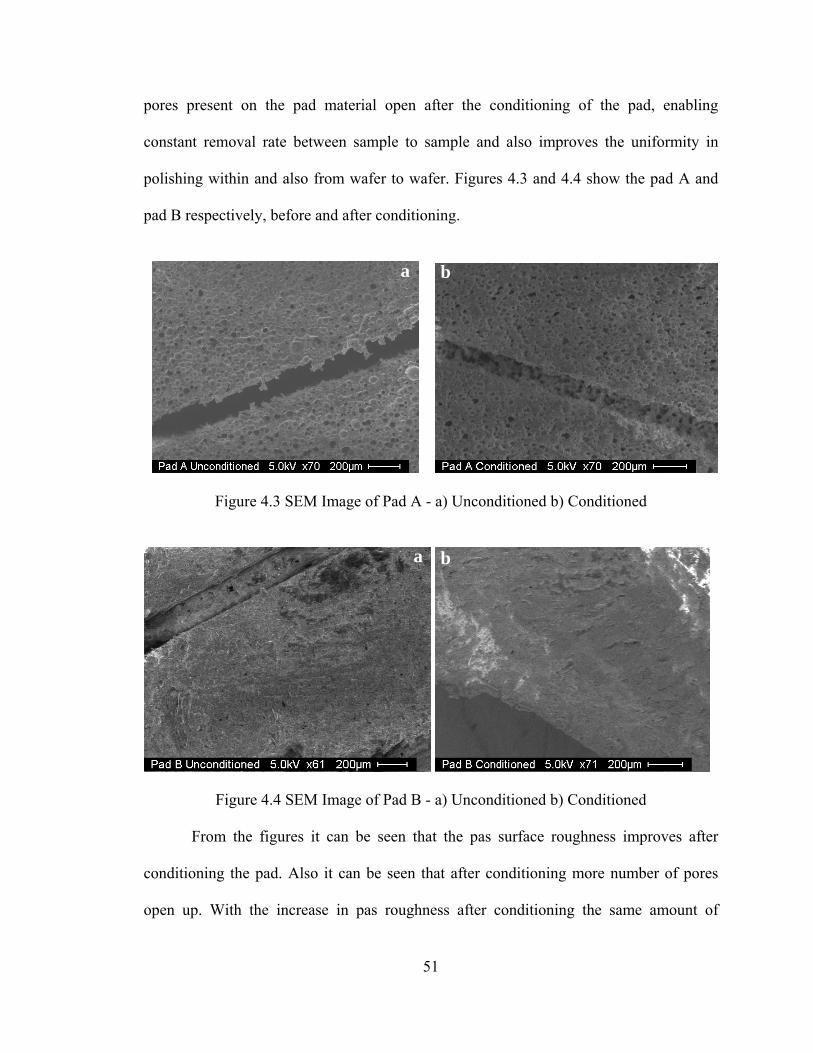
51
pores present on the pad material open after the conditioning of the pad, enabling
constant removal rate between sample to sample and also improves the uniformity in
polishing within and also from wafer to wafer. Figures 4.3 and 4.4 show the pad A and
pad B respectively, before and after conditioning.
Figure 4.3 SEM Image of Pad A - a) Unconditioned b) Conditioned
Figure 4.4 SEM Image of Pad B - a) Unconditioned b) Conditioned
From the figures it can be seen that the pas surface roughness improves after
conditioning the pad. Also it can be seen that after conditioning more number of pores
open up. With the increase in pas roughness after conditioning the same amount of
a b
a b
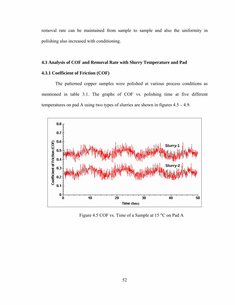
52
removal rate can be maintained from sample to sample and also the uniformity in
polishing also increased with conditioning.
4.3 Analysis of COF and Removal Rate with Slurry Temperature and Pad
4.3.1 Coefficient of Friction (COF)
The patterned copper samples were polished at various process conditions as
mentioned in table 3.1. The graphs of COF vs. polishing time at five different
temperatures on pad A using two types of slurries are shown in figures 4.5 – 4.9.
Figure 4.5 COF vs. Time of a Sample at 15 °C on Pad A
Slurry-1
Slurry-2
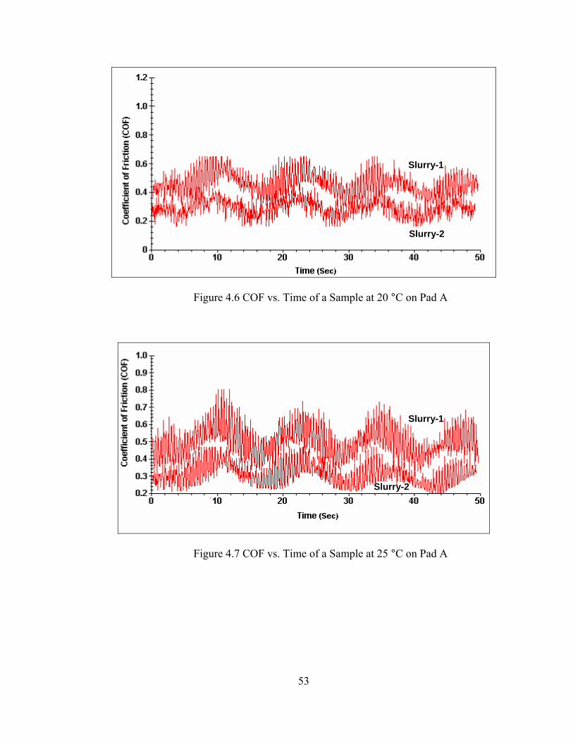
53
Figure 4.6 COF vs. Time of a Sample at 20 °C on Pad A
Figure 4.7 COF vs. Time of a Sample at 25 °C on Pad A
Slurry-1
Slurry-2
Slurry-1
Slurry-2
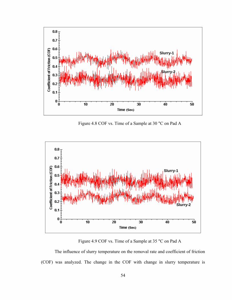
54
Figure 4.8 COF vs. Time of a Sample at 30 °C on Pad A
Figure 4.9 COF vs. Time of a Sample at 35 °C on Pad A
The influence of slurry temperature on the removal rate and coefficient of friction
(COF) was analyzed. The change in the COF with change in slurry temperature is
Slurry-1
Slurry-2
Slurry-1
Slurry-2
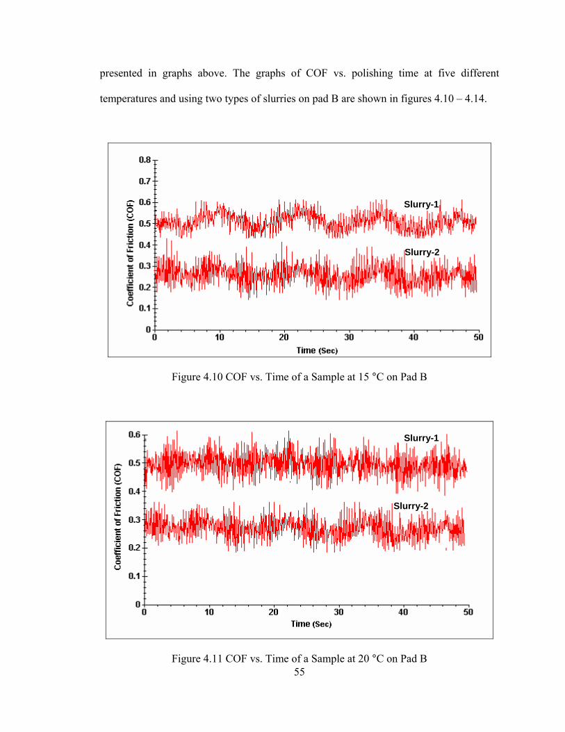
55
presented in graphs above. The graphs of COF vs. polishing time at five different
temperatures and using two types of slurries on pad B are shown in figures 4.10 – 4.14.
Figure 4.10 COF vs. Time of a Sample at 15 °C on Pad B
Figure 4.11 COF vs. Time of a Sample at 20 °C on Pad B
Slurry-1
Slurry-2
Slurry-1
Slurry-2
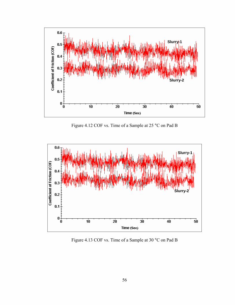
56
Figure 4.12 COF vs. Time of a Sample at 25 °C on Pad B
Figure 4.13 COF vs. Time of a Sample at 30 °C on Pad B
Slurry-1
Slurry-2
Slurry-1
Slurry-2

57
Figure 4.14 COF vs. Time of a Sample at 35 °C on Pad B
Table 4.1 and 4.2 show the COF values of samples polished at five different
slurry temperatures on two pads (pad A and pad B) and two slurries. Three replicates of
samples were taken at each slurry temperature. The average of the three replicates was
taken to plot the COF vs. slurry temperature graph. Figure 4.15 and 4.16 show the graphs
between COF at five different slurry temperatures taken on two different polishing pads
and using slurry 1 and slurry 2 respectively.
Table 4.1 Coefficient of Friction at Different Slurry Temperatures Using Slurry-1
15 ºC 20 ºC 25 ºC 30 ºC 35 ºC
1 0.4682 0.4822 0.4824 0.4856 0.4878
2 0.4785 0.4751 0.4821 0.4864 0.4872 3 0.4587 0.4736 0.4795 0.4803 0.4869
CO
F on
Pad
-
A
Average 0.4675 0.4769 0.4813 0.4841 0.4873 1 0.5048 0.5136 0.5199 0.5337 0.5449 2 0.5039 0.5143 0.5218 0.5348 0.5441 3 0.5044 0.5127 0.5228 0.5341 0.5435
CO
F on
Pad
-
B
Average 0.5043 0.5135 0.5215 0.5342 0.5441
Slurry-1
Slurry-2
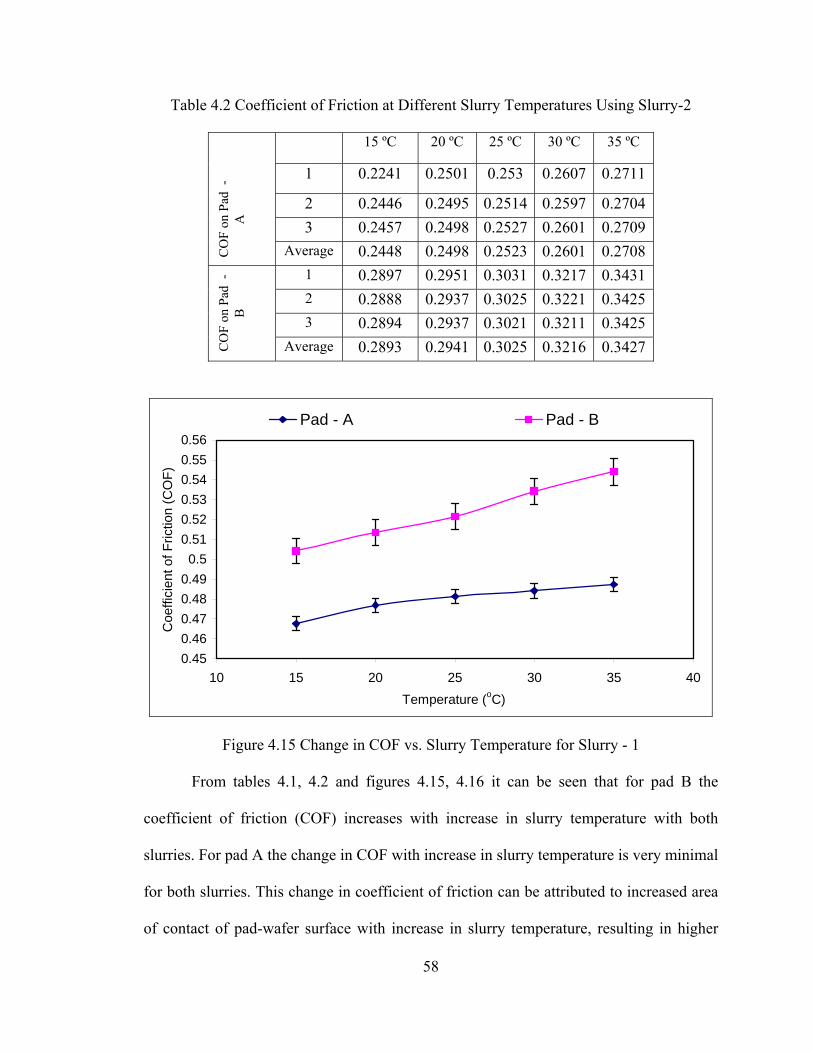
58
Table 4.2 Coefficient of Friction at Different Slurry Temperatures Using Slurry-2
15 ºC 20 ºC 25 ºC 30 ºC 35 ºC
1 0.2241 0.2501 0.253 0.2607 0.2711
2 0.2446 0.2495 0.2514 0.2597 0.2704 3 0.2457 0.2498 0.2527 0.2601 0.2709
CO
F on
Pad
-
A
Average 0.2448 0.2498 0.2523 0.2601 0.2708
1 0.2897 0.2951 0.3031 0.3217 0.3431 2 0.2888 0.2937 0.3025 0.3221 0.3425 3 0.2894 0.2937 0.3021 0.3211 0.3425
CO
F on
Pad
-
B
Average 0.2893 0.2941 0.3025 0.3216 0.3427
0.450.460.470.480.490.5
0.510.520.530.540.550.56
10 15 20 25 30 35 40Temperature (oC)
Coe
ffici
ent o
f Fric
tion
(CO
F)
Pad - A Pad - B
Figure 4.15 Change in COF vs. Slurry Temperature for Slurry - 1
From tables 4.1, 4.2 and figures 4.15, 4.16 it can be seen that for pad B the
coefficient of friction (COF) increases with increase in slurry temperature with both
slurries. For pad A the change in COF with increase in slurry temperature is very minimal
for both slurries. This change in coefficient of friction can be attributed to increased area
of contact of pad-wafer surface with increase in slurry temperature, resulting in higher
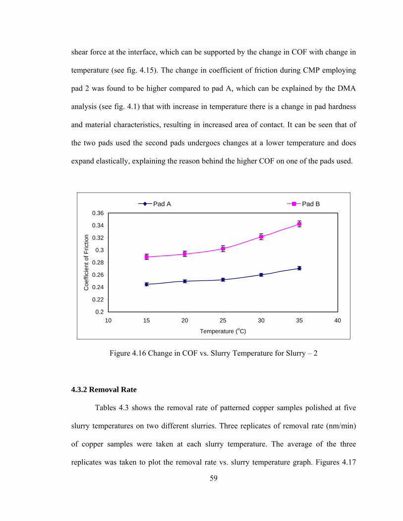
59
shear force at the interface, which can be supported by the change in COF with change in
temperature (see fig. 4.15). The change in coefficient of friction during CMP employing
pad 2 was found to be higher compared to pad A, which can be explained by the DMA
analysis (see fig. 4.1) that with increase in temperature there is a change in pad hardness
and material characteristics, resulting in increased area of contact. It can be seen that of
the two pads used the second pads undergoes changes at a lower temperature and does
expand elastically, explaining the reason behind the higher COF on one of the pads used.
0.2
0.22
0.24
0.26
0.28
0.3
0.32
0.34
0.36
10 15 20 25 30 35 40
Temperature (oC)
Coe
ffici
ent o
f Fric
tion
Pad A Pad B
Figure 4.16 Change in COF vs. Slurry Temperature for Slurry – 2
4.3.2 Removal Rate
Tables 4.3 shows the removal rate of patterned copper samples polished at five
slurry temperatures on two different slurries. Three replicates of removal rate (nm/min)
of copper samples were taken at each slurry temperature. The average of the three
replicates was taken to plot the removal rate vs. slurry temperature graph. Figures 4.17

60
and 4.18 shows the graphs between removal rates at three different slurry temperatures
taken on two different polishing pads.
Table 4.3 Removal Rates at Different Slurry Temperatures Using Slurry 1 and 2
15 ºC 20 ºC 25 ºC 30 ºC 35 ºC
Slurry - 1
190.5 222.2 255.3 285.7 333.3 R
emov
al R
ate
on P
ad -
A
(nm
/min
)
Slurry - 2
137.9 153.8 160 173.9 218.2
Slurry - 1
333.3 400 500 600 666.7
Rem
oval
Rat
e on
Pad
- B
(n
m/m
in)
Slurry - 2
153.8 181.8 200 222.3 272.7
0
100
200
300
400
500
600
700
800
10 15 20 25 30 35 40
Temperature (oC)
Rem
oval
Rat
e (n
m/m
in)
Pad - A Pad - B
Figure 4.17 Removal Rate vs. Slurry Temperature Using Slurry-1
From table 4.3 and figures 4.17 and 4.18 it can be seen that removal rate increases
with increase in slurry temperature for pad A and pad B polishing pads. The removal rate
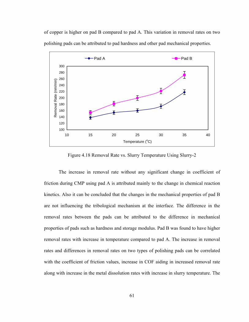
61
of copper is higher on pad B compared to pad A. This variation in removal rates on two
polishing pads can be attributed to pad hardness and other pad mechanical properties.
100
120
140
160
180
200
220
240
260
280
300
10 15 20 25 30 35 40
Temperature (oC)
Rem
oval
Rat
e (n
m/m
in)
Pad A Pad B
Figure 4.18 Removal Rate vs. Slurry Temperature Using Slurry-2
The increase in removal rate without any significant change in coefficient of
friction during CMP using pad A is attributed mainly to the change in chemical reaction
kinetics. Also it can be concluded that the changes in the mechanical properties of pad B
are not influencing the tribological mechanism at the interface. The difference in the
removal rates between the pads can be attributed to the difference in mechanical
properties of pads such as hardness and storage modulus. Pad B was found to have higher
removal rates with increase in temperature compared to pad A. The increase in removal
rates and differences in removal rates on two types of polishing pads can be correlated
with the coefficient of friction values, increase in COF aiding in increased removal rate
along with increase in the metal dissolution rates with increase in slurry temperature. The

62
increase in the coefficient of friction and material removal rate with increase in slurry
temperature compares well with literature [1].
4.4 Analysis of Dishing with Slurry Temperature and Pad
The patterned copper samples polished at five different slurry temperatures were
analyzed for the amount of dishing on 10 µm, 20 µm and 50 µm wide metal lines and on
100 µm square bond pads using profilometer and atomic force microscopy (AFM). Table
4.4 gives the values of the normalized dishing data on the metal lines and the bond pads
using two slurries. Figures 4.19 and 4.20 show the amount of dishing on a 10 µm wide
metal line at different slurry temperatures on different pads using two slurries. The
amount of dishing (nm) has been normalized for analysis.
Table 4.4 Normalized Dishing Data on Metal Lines and Bond Pads
10 µm wide metal line
20 µm wide metal line
50 µm wide metal line
100 µm bond pads
Slurry Temperatur
e (ºC) Pad A Pad B Pad A Pad B Pad A Pad B Pad A Pad B 15 ºC 0.0307 0.075 0.1194 0.1358 0.5881 0.5120 0.6336 0.481
20 ºC 0.0848 0.114 0.1441 0.1619 0.7586 0.6003 0.7108 0.564
25ºC 0.1364 0.1531 0.1839 0.191 0.8651 0.698 0.9132 0.651
30ºC 0.1657 0.1868 0.2146 0.225 0.9098 0.8218 1 0.747 Slur
ry -
1
35ºC 0.1502 0.1647 0.1927 0.2078 0.8825 0.7791 0.98 0.665
15ºC 0.0282 0.0986 0.0594 0.1425 0.483 0.8786 0.5204 1
20ºC 0.0184 0.0804 0.0409 0.1146 0.4005 0.8199 0.2134 0.933
25ºC 0.0116 0.0685 0.0294 0.0977 0.254 0.7981 0.167 0.889
30ºC 0.0084 0.0525 0.0238 0.0746 0.1615 0.7779 0.1543 0.843 Slur
ry -
2
35ºC 0.0078 0.035 0.020 0.0595 0.066 0.7592 0.1202 0.779
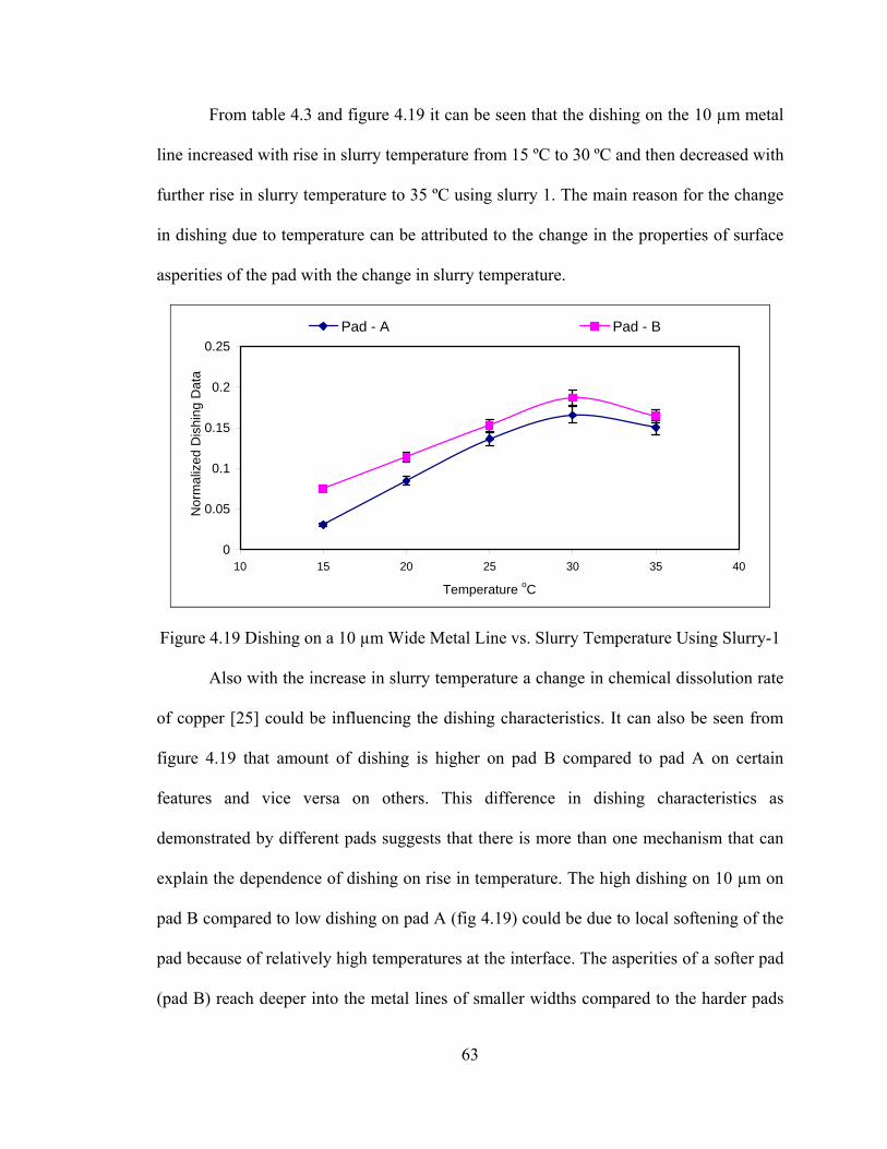
63
From table 4.3 and figure 4.19 it can be seen that the dishing on the 10 µm metal
line increased with rise in slurry temperature from 15 ºC to 30 ºC and then decreased with
further rise in slurry temperature to 35 ºC using slurry 1. The main reason for the change
in dishing due to temperature can be attributed to the change in the properties of surface
asperities of the pad with the change in slurry temperature.
0
0.05
0.1
0.15
0.2
0.25
10 15 20 25 30 35 40
Temperature oC
Nor
mal
ized
Dis
hing
Dat
a
Pad - A Pad - B
Figure 4.19 Dishing on a 10 µm Wide Metal Line vs. Slurry Temperature Using Slurry-1
Also with the increase in slurry temperature a change in chemical dissolution rate
of copper [25] could be influencing the dishing characteristics. It can also be seen from
figure 4.19 that amount of dishing is higher on pad B compared to pad A on certain
features and vice versa on others. This difference in dishing characteristics as
demonstrated by different pads suggests that there is more than one mechanism that can
explain the dependence of dishing on rise in temperature. The high dishing on 10 µm on
pad B compared to low dishing on pad A (fig 4.19) could be due to local softening of the
pad because of relatively high temperatures at the interface. The asperities of a softer pad
(pad B) reach deeper into the metal lines of smaller widths compared to the harder pads

64
(pad A), resulting in increase of dishing. This change in pad physical properties with
increase in slurry temperature is well explained with the help of dynamic mechanical
analysis (DMA) of polishing pad, presented in the following sections. From figure 4.20 it
can be seen that the dishing values on two types of polishing pads decrease with increase
in slurry temperature using slurry 2.
0
0.02
0.04
0.06
0.08
0.1
0.12
10 15 20 25 30 35 40
Temperature oC
Nor
mal
ized
Dis
hing
Dat
a
Pad - A Pad - B
Figure 4.20 Dishing on a 10 µm Wide Metal Line vs. Slurry Temperature Using Slurry-2
This may be due to the reason that the slurry 2 had a different oxidizer
(Ammonium per sulfate) and when compared with slurry -1 the oxidation rate is low and
also reactivity’s of both the slurries with pad is different. Also the chemical nature of the
slurries is suspected to play an important role in determining the change in dishing with
change in temperature. It can be noted that also with slurry 2 the pad B has higher amount
of dishing when compared to pad A.
Figures 4.21 and 4.22 show the normalized dishing on a 20 µm wide metal line
with increase in slurry temperature. However, as the line width increases, on a 20 µm
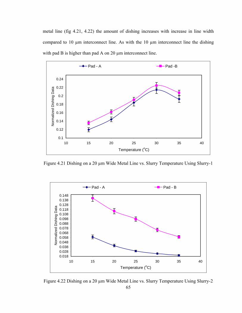
65
metal line (fig 4.21, 4.22) the amount of dishing increases with increase in line width
compared to 10 µm interconnect line. As with the 10 µm interconnect line the dishing
with pad B is higher than pad A on 20 µm interconnect line.
0.1
0.12
0.14
0.16
0.18
0.2
0.22
0.24
10 15 20 25 30 35 40
Temperature (oC)
Nor
mal
ized
Dis
hing
Dat
a
Pad - A Pad -B
Figure 4.21 Dishing on a 20 µm Wide Metal Line vs. Slurry Temperature Using Slurry-1
0.0180.0280.0380.0480.0580.0680.0780.0880.0980.1080.1180.1280.1380.148
10 15 20 25 30 35 40
Temperature (oC)
Nor
mal
ized
Dis
hing
Dat
a
Pad - A Pad - B
Figure 4.22 Dishing on a 20 µm Wide Metal Line vs. Slurry Temperature Using Slurry-2
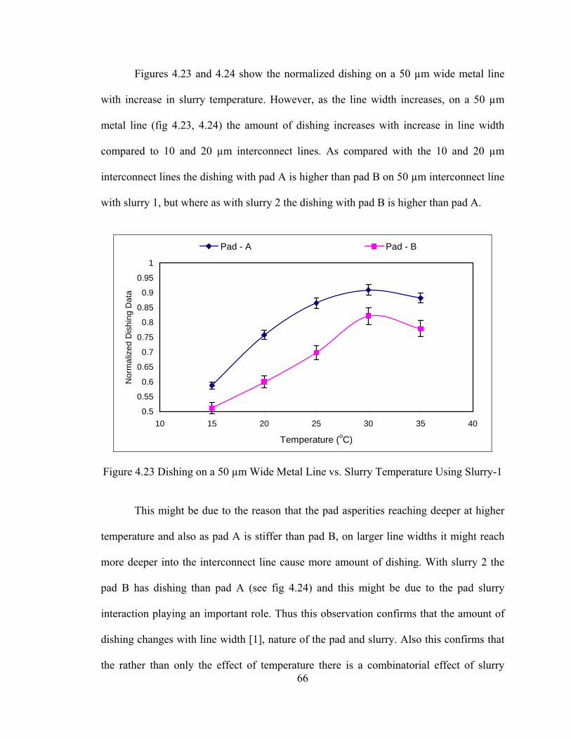
66
Figures 4.23 and 4.24 show the normalized dishing on a 50 µm wide metal line
with increase in slurry temperature. However, as the line width increases, on a 50 µm
metal line (fig 4.23, 4.24) the amount of dishing increases with increase in line width
compared to 10 and 20 µm interconnect lines. As compared with the 10 and 20 µm
interconnect lines the dishing with pad A is higher than pad B on 50 µm interconnect line
with slurry 1, but where as with slurry 2 the dishing with pad B is higher than pad A.
0.5
0.55
0.6
0.65
0.7
0.75
0.8
0.85
0.9
0.95
1
10 15 20 25 30 35 40
Temperature (oC)
Nor
mal
ized
Dis
hing
Dat
a
Pad - A Pad - B
Figure 4.23 Dishing on a 50 µm Wide Metal Line vs. Slurry Temperature Using Slurry-1
This might be due to the reason that the pad asperities reaching deeper at higher
temperature and also as pad A is stiffer than pad B, on larger line widths it might reach
more deeper into the interconnect line cause more amount of dishing. With slurry 2 the
pad B has dishing than pad A (see fig 4.24) and this might be due to the pad slurry
interaction playing an important role. Thus this observation confirms that the amount of
dishing changes with line width [1], nature of the pad and slurry. Also this confirms that
the rather than only the effect of temperature there is a combinatorial effect of slurry
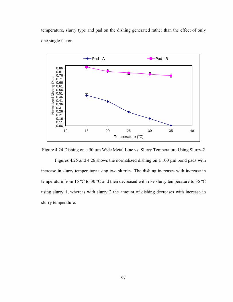
67
temperature, slurry type and pad on the dishing generated rather than the effect of only
one single factor.
0.060.110.160.210.260.310.360.410.460.510.560.610.660.710.760.810.86
10 15 20 25 30 35 40
Temperature (oC)
Nor
mal
ized
Dis
hing
Dat
a
Pad - A Pad - B
Figure 4.24 Dishing on a 50 µm Wide Metal Line vs. Slurry Temperature Using Slurry-2
Figures 4.25 and 4.26 shows the normalized dishing on a 100 µm bond pads with
increase in slurry temperature using two slurries. The dishing increases with increase in
temperature from 15 ºC to 30 ºC and then decreased with rise slurry temperature to 35 ºC
using slurry 1, whereas with slurry 2 the amount of dishing decreases with increase in
slurry temperature.
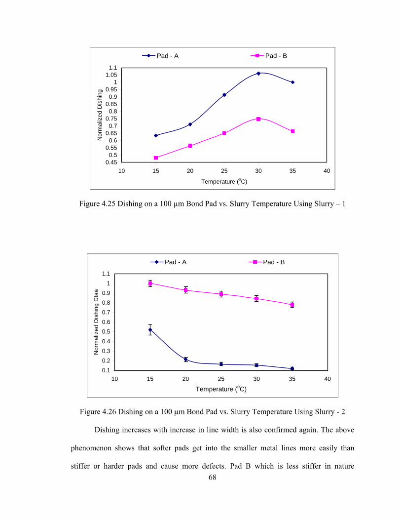
68
0.450.5
0.550.6
0.650.7
0.750.8
0.850.9
0.951
1.051.1
10 15 20 25 30 35 40
Temperature (oC)
Nor
mal
ized
Dis
hing
Pad - A Pad - B
Figure 4.25 Dishing on a 100 µm Bond Pad vs. Slurry Temperature Using Slurry – 1
0.10.20.30.40.50.60.70.80.9
11.1
10 15 20 25 30 35 40
Temperature (oC)
Nor
mal
ized
Dis
hing
Dta
a
Pad - A Pad - B
Figure 4.26 Dishing on a 100 µm Bond Pad vs. Slurry Temperature Using Slurry - 2
Dishing increases with increase in line width is also confirmed again. The above
phenomenon shows that softer pads get into the smaller metal lines more easily than
stiffer or harder pads and cause more defects. Pad B which is less stiffer in nature
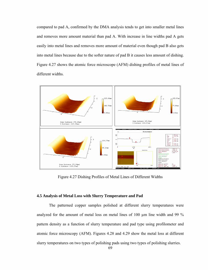
69
compared to pad A, confirmed by the DMA analysis tends to get into smaller metal lines
and removes more amount material than pad A. With increase in line widths pad A gets
easily into metal lines and removes more amount of material even though pad B also gets
into metal lines because due to the softer nature of pad B it causes less amount of dishing.
Figure 4.27 shows the atomic force microscope (AFM) dishing profiles of metal lines of
different widths.
Figure 4.27 Dishing Profiles of Metal Lines of Different Widths
4.5 Analysis of Metal Loss with Slurry Temperature and Pad
The patterned copper samples polished at different slurry temperatures were
analyzed for the amount of metal loss on metal lines of 100 µm line width and 99 %
pattern density as a function of slurry temperature and pad type using profilometer and
atomic force microscopy (AFM). Figures 4.28 and 4.29 show the metal loss at different
slurry temperatures on two types of polishing pads using two types of polishing slurries.

70
It can be seen from figure 4.28 that the amount of metal loss is higher with pad A
than with pad B. The area of the feature on which the metal loss was measured has
dimensions in the order of 1500 µm. The reason for higher metal loss with pad A could
be that the reaching of asperities of pad A well into the metal lines as well as the
dielectric material is the dominating factor as compared to the hardness of the pad. From
this we can infer that pad asperity interaction with the feature and the bulk hardness of
the pad both have a combinatorial effect on dishing.
0.30.330.360.390.420.450.480.510.540.57
0.60.630.66
10 15 20 25 30 35 40
Temperature (oC)
Nor
mal
ized
Met
al L
oss
Dat
aa
Pad - A Pad - B
Figure 4.28 Metal Loss vs. Slurry Temperature Using Slurry - 1
Figure 4.29 shows the metal loss on the two types of polishing pads using slurry
2. The amount of metal loss decreases with increase in slurry temperature, pad B having
more amount of metal loss than pad A
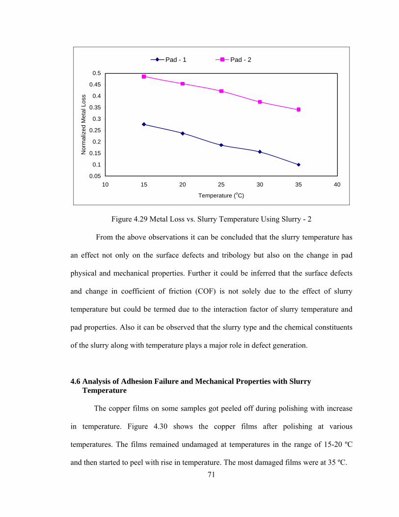
71
0.05
0.1
0.15
0.2
0.25
0.3
0.35
0.4
0.45
0.5
10 15 20 25 30 35 40
Temperature (oC)
Nor
mal
ized
Met
al L
oss
Pad - 1 Pad - 2
Figure 4.29 Metal Loss vs. Slurry Temperature Using Slurry - 2
From the above observations it can be concluded that the slurry temperature has
an effect not only on the surface defects and tribology but also on the change in pad
physical and mechanical properties. Further it could be inferred that the surface defects
and change in coefficient of friction (COF) is not solely due to the effect of slurry
temperature but could be termed due to the interaction factor of slurry temperature and
pad properties. Also it can be observed that the slurry type and the chemical constituents
of the slurry along with temperature plays a major role in defect generation.
4.6 Analysis of Adhesion Failure and Mechanical Properties with Slurry Temperature
The copper films on some samples got peeled off during polishing with increase
in temperature. Figure 4.30 shows the copper films after polishing at various
temperatures. The films remained undamaged at temperatures in the range of 15-20 ºC
and then started to peel with rise in temperature. The most damaged films were at 35 ºC.
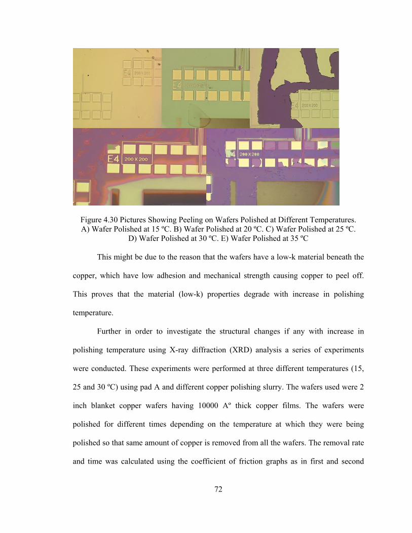
72
Figure 4.30 Pictures Showing Peeling on Wafers Polished at Different Temperatures. A) Wafer Polished at 15 ºC. B) Wafer Polished at 20 ºC. C) Wafer Polished at 25 ºC.
D) Wafer Polished at 30 ºC. E) Wafer Polished at 35 ºC
This might be due to the reason that the wafers have a low-k material beneath the
copper, which have low adhesion and mechanical strength causing copper to peel off.
This proves that the material (low-k) properties degrade with increase in polishing
temperature.
Further in order to investigate the structural changes if any with increase in
polishing temperature using X-ray diffraction (XRD) analysis a series of experiments
were conducted. These experiments were performed at three different temperatures (15,
25 and 30 ºC) using pad A and different copper polishing slurry. The wafers used were 2
inch blanket copper wafers having 10000 Aº thick copper films. The wafers were
polished for different times depending on the temperature at which they were being
polished so that same amount of copper is removed from all the wafers. The removal rate
and time was calculated using the coefficient of friction graphs as in first and second
A B C
D E
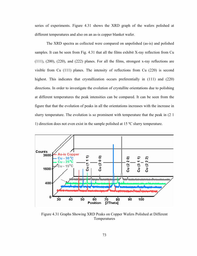
73
series of experiments. Figure 4.31 shows the XRD graph of the wafers polished at
different temperatures and also on an as-is copper blanket wafer.
The XRD spectra as collected were compared on unpolished (as-is) and polished
samples. It can be seen from Fig. 4.31 that all the films exhibit X-ray reflection from Cu
(111), (200), (220), and (222) planes. For all the films, strongest x-ray reflections are
visible from Cu (111) planes. The intensity of reflections from Cu (220) is second
highest. This indicates that crystallization occurs preferentially in (111) and (220)
directions. In order to investigate the evolution of crystallite orientations due to polishing
at different temperatures the peak intensities can be compared. It can be seen from the
figure that that the evolution of peaks in all the orientations increases with the increase in
slurry temperature. The evolution is so prominent with temperature that the peak in (2 1
1) direction does not even exist in the sample polished at 15 ºC slurry temperature.
Figure 4.31 Graphs Showing XRD Peaks on Copper Wafers Polished at Different Temperatures

74
Also from the XRD measurements as shown in figure 4.31, an additional peak at
32 deg diffraction angle was observed on the sample polished at 30 oC temperature. This
indicates that the copper crystallinity increases with increasing polishing temperature. As
the crystallinity increases, the mechanical characteristics improve as well and this was
confirmed with the hardness tests conducted on the samples using a nano-indenter.
Figure 4.32 presents the hardness of the unpolished film and for the films post
CMP at different temperatures. From figure 4.32 it can be noted that the hardness of the
polished copper surface increased with increasing slurry temperature. The unpolished
sample had significantly lower hardness than the polished ones. This change can be
attributed to the work hardening phenomenon during CMP. The work hardening
phenomenon appears to be more influential at elevated temperatures. Similarly the
modulus of the polished and unpolished thin films along the penetration depth is
presented in figure 4.33. It can be seen that the modulus of elasticity increases with
increasing slurry temperature. Also, the modulus of elasticity of the unpolished film is
significantly lower than that of the polished samples. The numerical data from the
nanoindentation experiments is presented in table 4.5 which presents in detail the change
in mechanical properties of thin films with a change in slurry temperature.
Table 4.5 Mechanical Properties of Copper Thin Films Before and After Polishing
Sample Modulus (Gpa) Hardness (Gpa) Unpolished Cu 118.51 ± 3.72 1.22 ± 0.06 Polished at 15 C 136.38 ± 5.45 1.57 ± 0.087 Polished at 25 C 136.29 ± 4.77 1.66 ± 0.093 Polished at 30 C 143.45 ± 2.98 1.72 ± 0.068

75
0
1
2
3
4
5
6
0 50 100 150Displacement Into Surface (nm)
Har
dnes
s (G
Pa)
15 C 30 C 25 C unpolished
Figure 4.32 Hardness vs. Displacement into Surface for Unpolished and Polished Copper Samples
50
100
150
200
250
0 50 100 150
Displacement Into Surface (nm)
Mod
ulus
(GP
a)
15 C30 C25 Cunpolished
Figure 4.33 Modulus vs. Displacement into Surface for Polished and Unpolished Copper Samples

76
4.7 Analysis of Electrical Properties with Slurry Temperature
In order to further investigate the effects of surface defects, due rise in polishing
temperature on device operating characteristics the second series of experiments were
carried out. These experiments were carried on same types of polishing pads (pad 1 & 2)
and with same slurry, other parameters remaining the same. The fabricated PMOS
devices had similar feature sizes of 10, 20 & 50 µm and bond pads of 100 µm in
dimensions as in first set of experiments.
The dishing values and metal loss values were almost numerically similar to the
values obtained in the first set of experiments. Then the polished samples were tested for
the I-V characteristics using HP 4145B parameter analyzer. Figures 4.34, 4.35 show the
transfer curves and sub threshold log plots I-V characteristics of the devices polished at
different temperatures.
For the drain characteristics the drain to source voltage (VDS) was swept from 0 to
-15 V and the gate to source voltage (VGS) was increased in steps from 0 to -15 V and the
corresponding values of drain current (ID) were recorded. In order to explain the shape of
drain characteristics the curve may be divided into four regions as shown in figure 13a.
The first region in the curve shown as 0A is the ohmic region. In this region the drain
current increases linearly with increase in drain voltage, obeying Ohm’s law. In the next
region (AB) the drain current increases according to the reverse square law. Here the
drain current increases slowly as compared to the ohmic region. This occurs due to the
fact that with increase in VD, the ID increases. As a result of this, the size of the depletion
region becomes bigger, reducing the effective width of the channel. The region under the
curve BC is the saturation or the constant current region. Here the drain current reaches
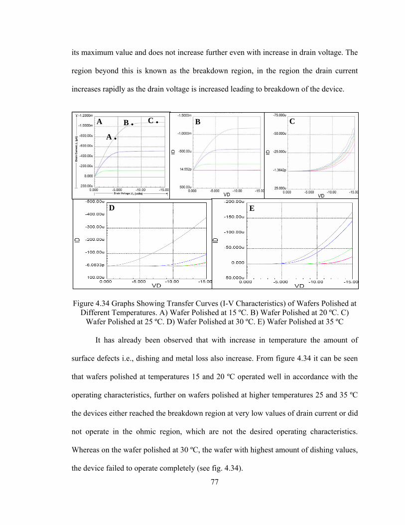
77
its maximum value and does not increase further even with increase in drain voltage. The
region beyond this is known as the breakdown region, in the region the drain current
increases rapidly as the drain voltage is increased leading to breakdown of the device.
Figure 4.34 Graphs Showing Transfer Curves (I-V Characteristics) of Wafers Polished at
Different Temperatures. A) Wafer Polished at 15 ºC. B) Wafer Polished at 20 ºC. C) Wafer Polished at 25 ºC. D) Wafer Polished at 30 ºC. E) Wafer Polished at 35 ºC
It has already been observed that with increase in temperature the amount of
surface defects i.e., dishing and metal loss also increase. From figure 4.34 it can be seen
that wafers polished at temperatures 15 and 20 ºC operated well in accordance with the
operating characteristics, further on wafers polished at higher temperatures 25 and 35 ºC
the devices either reached the breakdown region at very low values of drain current or did
not operate in the ohmic region, which are not the desired operating characteristics.
Whereas on the wafer polished at 30 ºC, the wafer with highest amount of dishing values,
the device failed to operate completely (see fig. 4.34).
A B C
D E
A . B . C .
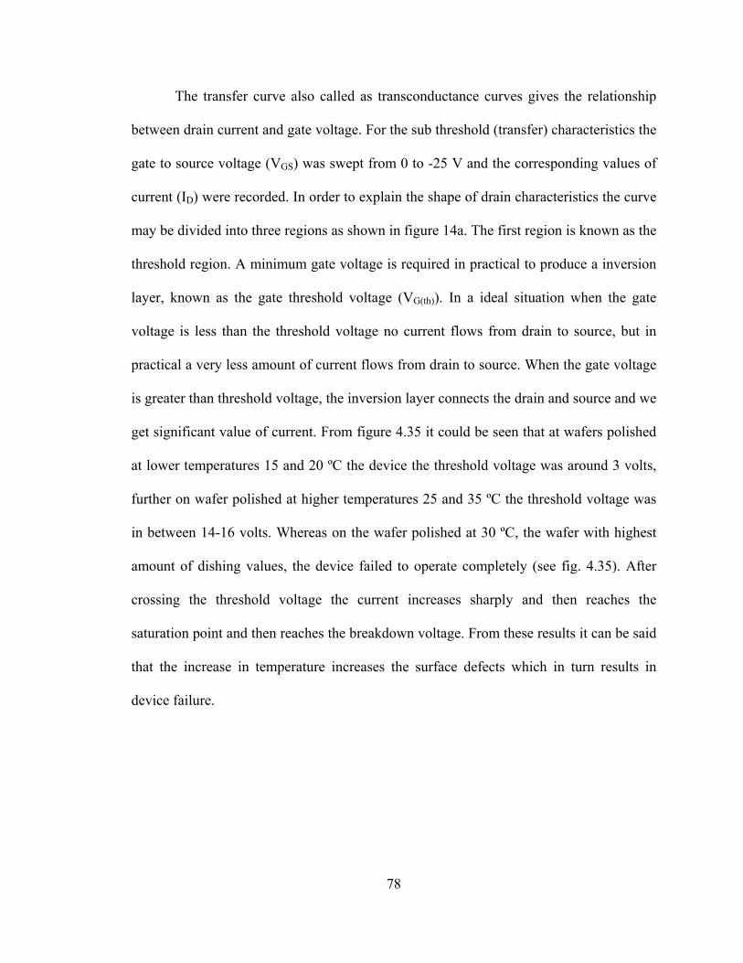
78
The transfer curve also called as transconductance curves gives the relationship
between drain current and gate voltage. For the sub threshold (transfer) characteristics the
gate to source voltage (VGS) was swept from 0 to -25 V and the corresponding values of
current (ID) were recorded. In order to explain the shape of drain characteristics the curve
may be divided into three regions as shown in figure 14a. The first region is known as the
threshold region. A minimum gate voltage is required in practical to produce a inversion
layer, known as the gate threshold voltage (VG(th)). In a ideal situation when the gate
voltage is less than the threshold voltage no current flows from drain to source, but in
practical a very less amount of current flows from drain to source. When the gate voltage
is greater than threshold voltage, the inversion layer connects the drain and source and we
get significant value of current. From figure 4.35 it could be seen that at wafers polished
at lower temperatures 15 and 20 ºC the device the threshold voltage was around 3 volts,
further on wafer polished at higher temperatures 25 and 35 ºC the threshold voltage was
in between 14-16 volts. Whereas on the wafer polished at 30 ºC, the wafer with highest
amount of dishing values, the device failed to operate completely (see fig. 4.35). After
crossing the threshold voltage the current increases sharply and then reaches the
saturation point and then reaches the breakdown voltage. From these results it can be said
that the increase in temperature increases the surface defects which in turn results in
device failure.
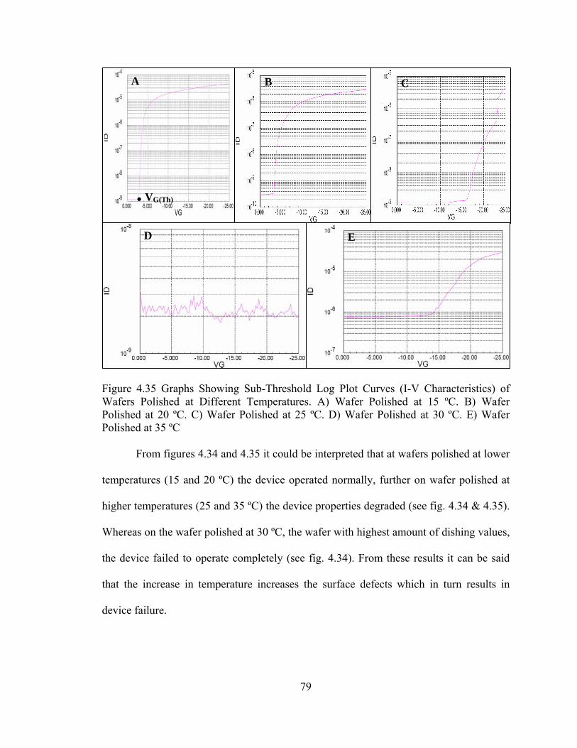
79
Figure 4.35 Graphs Showing Sub-Threshold Log Plot Curves (I-V Characteristics) of Wafers Polished at Different Temperatures. A) Wafer Polished at 15 ºC. B) Wafer Polished at 20 ºC. C) Wafer Polished at 25 ºC. D) Wafer Polished at 30 ºC. E) Wafer Polished at 35 ºC
From figures 4.34 and 4.35 it could be interpreted that at wafers polished at lower
temperatures (15 and 20 ºC) the device operated normally, further on wafer polished at
higher temperatures (25 and 35 ºC) the device properties degraded (see fig. 4.34 & 4.35).
Whereas on the wafer polished at 30 ºC, the wafer with highest amount of dishing values,
the device failed to operate completely (see fig. 4.34). From these results it can be said
that the increase in temperature increases the surface defects which in turn results in
device failure.
A B C
D E
. VG(Th)
80
4.8 Summary
The effect of slurry temperature at three temperatures on two different pads were
investigated, keeping the pressure and platen velocity constant. The patterned copper
samples were characterized using the AFM and profilometer. The characteristics of two
different kinds of pads were analyzed using DMA. From the DMA analysis it could be
inferred that pad softens with increase in temperature and pad B is softer in nature
compared to pad A. Within the operating range there is greater percentage of decrease in
storage modulus of pad B compared to pad A. From SEM analysis it was found that pad
conditioning improved the uniformity of polish and also increased the roughness of the
polishing pad. It was found that the COF on pad A increased with increase in slurry
temperature and on pad B the variation in COF with increase in slurry temperature was
found to be statistically insignificant. This change in COF on the pads can be attributed to
the pad physical properties. The removal rates on both the pads increased with increase in
slurry temperature. However the removal rate on pad A was higher than the removal rates
on pad B. This increase in removal rate and the difference in the amount of removal rates
on both pads can be attributed to the change in the rate of kinetics of chemical reactions
and also to the mechanical properties of the pad.
The dishing initially increased with increase in temperature upto 30 oC and then
decreased with further increase in temperature using slurry 1, whereas the dishing
decreased with increase in slurry temperature using slurry 2. This could be attributed to
the change in the properties of surface asperities of the pad. This could be well explained
with the DMA analysis of pad materials. It further concluded that the dishing was
dependent on the interaction factor of slurry temperature, slurry type (chemical
81
constituents of the slurry) and change in pad properties with temperature, than as initially
thought would be due to slurry temperature. Also changes in copper structural properties
were observed with increase in slurry temperature. The device electrical properties
degraded drastically with increasing slurry temperature and even leading to device failure
at higher polishing temperatures.
82
Chapter 5
Conclusions and Future Work
The main objective of this research was to study the effect of slurry temperature
on defect generation and tribology during copper CMP. Surface defect generation on
patterned copper wafers with increase in slurry temperatures were tested using the CMP
tester at different temperatures and with two types of polishing pads. Post CMP analysis
of the polished samples was conducted using atomic force microscopy (AFM) and
profilometer. The mechanical and physical properties of the polishing pads used were
analyzed using dynamic mechanical analysis (DMA). Change in copper structural
properties was studied using X-ray diffraction (XRD) analysis. Also the device electrical
working characteristics were used on fabricated devices polished at different slurry
temperatures. Conclusions based on the research work and the results from previous
chapters are presented here.
5.1 Conclusions
5.1.1 Friction (COF) and Removal Rate Studies
• The coefficient of friction (COF) on pad A and pad B increased with the increase
in slurry temperature.
• This increase in coefficient of friction on pad A and pad B can be attributed to
increased area of contact of pad-wafer surface with increase in slurry temperature,
resulting in higher shear force at the interface.
83
• The removal rate increased with increase in slurry temperature on both pad A and
pad B.
• With increase in slurry temperature the removal rate on pad A was higher
compared to pad B depending on the interconnect line width.
• This variation in removal rates on two polishing pads can be attributed to pad
hardness and other pad mechanical properties. Also this variation can be
attributed to change in the rate of kinetics of chemical reactions with increase in
slurry temperature.
5.1.2 Dishing and Metal Loss
• The dishing and metal loss initially increased with increase in temperature from
15 °C to 30 °C and then decreased with further increase in temperature on both
pads with slurry-1.
• This phenomenon of increase in dishing and metal loss initially and then decrease
can be attributed to local softening of pad and change in pad physical and
mechanical properties.
• The dishing decreased with increase in slurry temperature using slurry-2. This
phenomenon can be attributed to the chemical nature (oxidizer and other
constituents of the slurry) of the slurry and its interaction with pad and also
change in its chemical properties with temperature rise.
• The different trend in dishing pattern with two different types of slurries is due to
change in pH of slurry with increase in temperature.
84
• The amount of dishing on 10 μm metal line was higher on pad B compared to pad
A, but whereas with increase in the line width the dishing with pad A is higher
than dishing on pad B.
• This variation in dishing with different types of pads can be attributed to change
in the properties of surface asperities of the pad and also change in chemical
dissolution rate.
• The DMA analysis confirms that with increase in temperature the pad becomes
softer.
• The amount of decrease in percentage of storage modulus of pad material is
higher for pad B compared to pad A. But in an ideal case there should be no
change in storage modulus for a polishing pad within the operating temperature
range.
• Pad B has lower glass transition temperature (Tg) compared to pad A. After
reaching Tg the pad transform from a glassy state into a rubbery state.
• Due to the softening of the pad with the increase in temperature the pad asperities
reach deeper into the metal lines and cause dishing and metal loss.
• Dishing and metal loss were dependent on the interaction factor of slurry
temperature and change in pad properties rather than only with the slurry
temperature.
• Also the uniformity in polishing improved with pad conditioning. The
conditioning also improved the roughness of the polishing pad.

85
5.1.3 Film Mechanical and Electrical Properties
• The films peeled off at higher temperatures. At 35 ºC the copper films on some of
the samples completely peeled off due to adhesion problems.
• The structural properties improved with increase in slurry temperature. There was
an increase in crystallinity of the copper thin films and also hardness and modulus
increased with increase in polishing temperature.
• An extra peak at (2 1 1) was observed on the film polished at 30 ºC indicating a
change in crystallinity.
• The electrical properties degraded drastically with increase in slurry temperature.
At the highest temperature the devices even failed to operate.
• The devices with minimal or mo dishing operated perfectly and exhibited good I-
V characteristics. The devices/wafers polished at 35 ºC failed to operate
completely.
5.2 Future Work
The effect of interaction of other process conditions such as pressure and velocity
with slurry temperature can be investigated. Also the effect of slurry temperature on
surface defects and tribology can be studied using various acidic and basic slurries and
also with various types of oxidizers and concentration of oxidizers. The effect of various
particles sizes, particle concentrations and different kinds of abrasive particles can be
studied. The effect of various orientations on pad surfaces such as grooves and
perforations along with different kinds of pad materials can be investigated. Also various
methods to reduce the temperature during polishing can be studied in order to reduce the

86
surface defects. The electrochemical analysis on different slurries can be done to get a
better understanding of change in slurry characteristics with change in temperature.
87
References
1. Joseph M. Steigerwald, Shyam P. Murarka, Ronald J. Gutmann, Chemical Mechanical Planarization of Microelectronic Materials, John Wiley and Sons, Inc. New York, (1997).
2. J.G. Ryan, R.M. Geffken, N.R. Poulin, J.R. Paraszczak, The Evolution of
Interconnection Technology at IBM, IBM J. Res. Dev., 39, 371, (1995).
3. S. Wolf, Silicon Processing For the VLSI Era, Vol. 4, Lattice Press, California, (2002).
4. Internet Website: http://www.itrs.net/Links/2005ITRS/Home2005.htm, ITRS,
(2005).
5. V. R. Kakireddy, R. Mudhivarthi, A. Kumar, P. Lefevre, Proc. VLSI Multilevel Interconnect Conference, 050, 415-420 (2006).
6. J. M. Steigerwald, S. P. Murarka, R. J. Gutmann, D. J. Duquette, Materials
Chemistry and Physics, 41, 217-228, (1995).
7. R. Carpio, J. Farkas, R. Jairath, Thin Solid Films, 266, 238-244, (1995).
8. Y. S. Obeng, J. E. Ramsdell, S. Deshpande, S. C. Kuiry, K. Chamma, K. A. Richardson, and S. Seal, IEEE Transactions on Semiconductor Manufacturing, 18, 4, (2005).
9. A. Ishikawa, H. Matsuo, T. Kikkawa, J.Electrochem. Soc. 152, (9), G695-G697,
(2005).
10. Z. Li, K. Ina, P. Lefevre, I. Koshiyama, A. Philipossian, J.Electrochem. Soc. 152, (4), G299-G304, (2005).
11. Y. Nomura, H. Ono, H. Terazaki, Y. Kamigata, M. Yoshida, Materials Research
Society Symp. Proc., 816, (2004).
12. Z. Li, P. Lefevre, I. Koshiyama, K. Ina, D. Boning, and A. Philipossian, IEEE
Transactions on Semiconductor Manufacturing, 18, 4, (2005).
13. H. Lu, B. Fookes, Y. Obeng, S. Machinski, K.A. Richardson, Materials Characterization, 49, 35-44, (2002).
88
14. H. Lu, Y. Obeng, K.A. Richardson, Materials Characterization, 49, 177-186,
(2003).
15. L. Wang, and F. M. Doyle, Proc. CMP Multilevel Interconnections Conference, (2004).
16. J. Sorooshian, D. DeNardis, L. Charns, Z. Li, F. Shadman, D. Boning, D.
Hetherington, and A. Philipossian, J. Electrochem. Soc., 151(2), G85-G88, (2004).
17. P. A. Miranda, J. A. Imonigie, A. L. Erbe, A. J. Moll, IEEE WMED, (2005).
18. T. H. Tsai, Y. F. Wu, S. C. Yen, Applied Surface Science, Article in press,
(2003).
19. P. A. Miranda, J. A. Imonigie, and A. J. Moll, J. Electrochem. Soc., 153(3), G211-G217, (2006).
20. P. Leduc, M. Savoye, S. Maitrejean, D. Scevola, V. Jousseaume, G. Passemard,
IEEE, (2005).
21. Q. Luo, D. R. Campbell, S. V. Babu, Thin Solid Films, 311, 177-182, (1997).
22. A. E. Miller, P. B. Fischer, A. D. Feller, K. C. Cadien, IEEE, 143-145, (2001).
23. T. Du, D. Tamboli, V. Desai, Microelectronic Engineering, 1, (2003).
24. S. Mudhivarthi, N. Gitis, S. Kuiry, M. Vinogradov, and A. Kumar, J.Electrochem. Soc. 153, (5), G372-G378, (2006).
25. S. Mudhviarthi et al, Electrochem. Solid-State Lett., 8, (9), G241-G245, (2005).
26. L. Borucki, Z. Li, and A. Philipossian, J. Electrochem. Soc., 151, G559 (2004)
27. Len Borucki, Leslie Charns and Ara Philipossian, J. Electrochem. Soc., 151, (12),
(2004), G809-G813.
28. Z. Li, L. Borucki, I. Koshiyama, and A. Philipossian, J. Electrochem. Soc., 151, (7), G482-G487, (2004).
29. V. R. K. Gorantla, K. A. Assiongbon, S. V. Babu, and D. Roy, J. Electrochem.
Soc., 152, (5), G404-G410, (2005).
30. V. R. K. Gorantla, A. Babel, S. Pandija, and S. V. Babu, Electrochem. Solid-State Lett., 8, (5), G131-G134, (2005).
89
31. J. M. Steigerwald, R. Zirpoli, S. P. Murarka, D. Price, and R. J. Gutmann, J. Electrochem. Soc., 141, 2842, (1994).
32. F. Preston, J. Soc. Glass Tech., 11, 214, (1927).
33. Internet Website: www.wikipedia.org.
34. S. Wolf, and R. N. Tauber, Silicon Processing For the VLSI Era, Vol. 1, Lattice
Press, California, (2000).
35. Internet Website: www.pubs.acs.org, American Chemical Society.
36. J. D. Reid, “Fundamentals of Copper Electroplating,” Semiconductor International, June 1998, p. 94.
37. Internet Website: www.mems-exchange.org.
38. V. M. Dubin et al, Proc. VLSI Multilevel Interconnect Conference, p. 315,
(1995).
39. P. B. Zantye, A. Kumar and A.K. Sikder “Chemical mechanical planarization for microelectronics applications”, Materials Science and Engineering: R: Reports, 45 (3-6) pp. 89 (2004).
40. H. H. Uhlig, Corrosion and Corrosion Control, John Wiley and Sons Inc., New
York, (1985).
41. M. R. Oliver, Chemical Mechanical Planarization of Semiconductor Materials, Springer Series in Materials Science, New York, (2004).
42. Internet Website: http://nnrc.eng.usf.edu, University of South Florida.
43. Internet Website: http://acept.la.asu.edu/PiN/rdg/elmicr/elmicr.shtml, Arizona
State University.
44. I. Li, K. M. Forsthoefel, K. A. Richardson, Y. S. Obeng, W. G. Easter, and A. Maury, Mat. Res. Soc. Symp., 613, (2000).
45. Kevin P. Menard, Dynamic Mechanical Analysis, CRC Press Inc., Florida,
(1999).
46. A. Tregub, M. Moinpur, and J. Sorooshian, “Effect of Temperature on Thermoanalytical Properties of Polishing Pads.”
47. J. Luo, D. A. Dornfeld, IEEE Transactions on Semiconductor Manufacturing, 14
(2), 112-133, 2001.
90
48. Internet Website: http://uweb.cas.usf.edu/~harmon, University of South Florida.
49. P. Singer, “Copper CMP: Taking aim at dishing,” Semiconductor International, October 2004.
50. G. Fu and A. Chandra, J. Electronic Materials, 31 (10), 1066-1073, 2002.
51. Internet Website: http://pubs.usgs.gov/of/2001/of01-
041/htmldocs/images/xrdschem.jpg.
52. N. Gitis, Semiconductor Fabtech, 18, 125 (2003).
53. N. Gitis, U.S. Pat. 6,494,765 (2002).
54. N. Gitis, U.S. Pat. 6,702,646 (2004).
55. N. Gitis and M. Vinogradov, in Proceedings of 2nd ICMI, Santa Clara, CA (2001).
56. A. Sikder, A. Kumar J. Electron. Mater., 30, 1520 (2001).


