
FN7330Rev 3.00
May 3, 2007
EL5100, EL5101, EL5300200MHz Slew Enhanced VFA
DATASHEET
The EL5100, EL5101, and EL5300 represent high-speed voltage feedback amplifiers based on the current feedback amplifier architecture. This gives the typical high slew rate benefits of a CFA family along with the stability and ease of use associated with the VFA type architecture. This family is available in single, dual, and triple versions, with 200MHz, 400MHz, and 700MHz versions. This family operates on single 5V or ±5V supplies from minimum supply current. The EL5100 and EL5300 also feature an output enable function, which can be used to put the output in to a high-impedance mode. This enables the outputs of multiple amplifiers to be tied together for use in multiplexing applications.
Features
• Pb-free plus anneal available (RoHS compliant)
• Specified for 5V or ±5V applications
• Power-down to 17µA/amplifier
• -3dB bandwidth = 200MHz
• ±0.1dB bandwidth = 20MHz
• Low supply current = 2.5mA
• Slew rate = 2200V/µs
• Low offset voltage = 4mV max
• Output current = 100mA
• AVOL = 1000
• Diff gain/phase = 0.08%/0.1°
Applications
• Video amplifiers
• PCMCIA applications
• A/D drivers
• Line drivers
• Portable computers
• High speed communications
• RGB applications
• Broadcast equipment
• Active filtering
FN7330 Rev 3.00 Page 1 of 15May 3, 2007

EL5100, EL5101, EL5300
Ordering Information
PART NUMBERPART
MARKING TAPE AND REEL PACKAGEPKG.
DWG. #
EL5100IS 5100IS - 8 Ld SOIC (150 mil) MDP0027
EL5100IS-T7 5100IS 7” 8 Ld SOIC (150 mil) MDP0027
EL5100IS-T13 5100IS 13” 8 Ld SOIC (150 mil) MDP0027
EL5100ISZ (Note) 5100ISZ - 8 Ld SOIC (150 mil) (Pb-free) MDP0027
EL5100ISZ-T7 (Note) 5100ISZ 7” 8 Ld SOIC (150 mil) (Pb-free) MDP0027
EL5100ISZ-T13 (Note) 5100ISZ 13” 8 Ld SOIC (150 mil) (Pb-free) MDP0027
EL5100IW-T7 y 7” (3k pcs) 6 Ld SOT-23 MDP0038
EL5100IW-T7A y 7” (250 pcs) 6 Ld SOT-23 MDP0038
EL5101IW-T7 2 7” (3k pcs) 5 Ld SOT-23 MDP0038
EL5101IW-T7A 2 7” (250 pcs) 5 Ld SOT-23 MDP0038
EL5300IU 5300IU - 16 Ld QSOP (150 mil) MDP0040
EL5300IU-T7 5300IU 7” 16 Ld QSOP (150 mil) MDP0040
EL5300IU-T13 5300IU 13” 16 Ld QSOP (150 mil) MDP0040
EL5300IUZ (Note) 5300IUZ - 16 Ld QSOP (150 mil) (Pb-free) MDP0040
EL5300IUZ-T7 (Note) 5300IUZ 7” 16 Ld QSOP (150 mil) (Pb-free) MDP0040
EL5300IUZ-T13 (Note) 5300IUZ 13” 16 Ld QSOP (150 mil) (Pb-free) MDP0040
NOTE: Intersil Pb-free plus anneal products employ special Pb-free material sets; molding compounds/die attach materials and 100% matte tin plate termination finish, which are RoHS compliant and compatible with both SnPb and Pb-free soldering operations. Intersil Pb-free products are MSL classified at Pb-free peak reflow temperatures that meet or exceed the Pb-free requirements of IPC/JEDEC J STD-020.
FN7330 Rev 3.00 Page 2 of 15May 3, 2007
EL5100, EL5101, EL5300
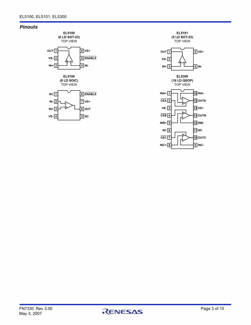
PinoutsEL5100
(6 LD SOT-23)TOP VIEW
EL5101(5 LD SOT-23)
TOP VIEW
EL5100(8 LD SOIC)TOP VIEW
EL5300(16 LD QSOP)
TOP VIEW
1
2
3
6
4
5+ -
OUT
VS-
IN+
VS+
ENABLE
IN-
1
2
3
5
4
+ -
OUT
VS-
IN+
VS+
IN-
1
2
3
4
8
7
6
5
-+
NC
IN-
IN+
ENABLE
VS+
OUT
VS- NC
1
2
3
4
16
15
14
13
5
6
7
12
11
10
8 9
-+
-+
-+
INA+
CEA
VS-
CEB
INA-
OUTA
VS+
OUTB
INB+
NC
CEC
INC+
INB-
NC
OUTC
INC-
FN7330 Rev 3.00 Page 3 of 15May 3, 2007

EL5100, EL5101, EL5300
Absolute Maximum Ratings (TA = +25°C) Thermal Information
Supply Voltage between VS+ and VS- . . . . . . . . . . . . . . . . . . . 13.2VInput Voltage . . . . . . . . . . . . . . . . . . . . . . . . . . . . . . . . . . . . . . . .±VSDifferential Input Voltage . . . . . . . . . . . . . . . . . . . . . . . . . . . . . . .±4VMaximum Output Current. . . . . . . . . . . . . . . . . . . . . . . . . . . . . 80mAMaximum Slewrate from VS+ to VS- . . . . . . . . . . . . . . . . . . . . 1V/µs
Storage Temperature Range . . . . . . . . . . . . . . . . . . -65°C to +150°CAmbient Operating Temperature Range . . . . . . . . . . -40°C to +85°COperating Junction Temperature . . . . . . . . . . . . . . . . . . . . . . +150°CPb-free reflow profile . . . . . . . . . . . . . . . . . . . . . . . . . .see link below
http://www.intersil.com/pbfree/Pb-FreeReflow.asp
CAUTION: Stresses above those listed in “Absolute Maximum Ratings” may cause permanent damage to the device. This is a stress only rating and operation of thedevice at these or any other conditions above those indicated in the operational sections of this specification is not implied.
IMPORTANT NOTE: All parameters having Min/Max specifications are guaranteed. Typical values are for information purposes only. Unless otherwise noted, all testsare at the specified temperature and are pulsed tests, therefore: TJ = TC = TA
DC Electrical Specifications VS = ±5V, GND = 0V, TA = +25°C, VCM = 0V, VOUT = 0V, VENABLE = GND or OPEN, Unless Otherwise
Specified.
PARAMETER DESCRIPTION CONDITIONS MIN TYP MAX UNIT
VOS Offset Voltage -4 1 4 mV
TCVOS Offset Voltage Temperature Coefficient Measured from TMIN to TMAX 8 µV/°C
IB Input Bias Current VIN = 0V -6 2 6 µA
IOS Input Offset Current VIN = 0V -2.5 0.5 2.5 µA
TCIOS Input Bias Current Temperature Coefficient
Measured from TMIN to TMAX 8 nA/°C
PSRR Power Supply Rejection Ratio 70 90 dB
CMRR Common Mode Rejection Ratio VCM from -3V to +3V 60 75 dB
CMIR Common Mode Input Range Guaranteed by CMRR test -3 +3 V
RIN Input Resistance VIN = -3V to +3V 0.7 1.2 M
CIN Input Capacitance 1 pF
IS,ON Supply Current - Enabled Per amplifier 2.1 2.5 2.9 mA
IS,OFF Supply Current - Shut Down VS+, per amplifier -5 0 5 µA
VS-, per amplifier 5 17 25 µA
PSOR Power Supply Operating Range 3.3 12 V
AVOL Open Loop Gain RL = 1k to GND, VOUT from -2.5V to +2.5V 55 60 dB
VOP Positive Output Voltage Swing RL = 150 to GND 3.2 3.4 V
RL = 1k to GND 3.6 3.8 V
VON Negative Output Voltage Swing RL = 150 to GND -3.4 -3.2 V
RL = 1k to GND -3.8 -3.6 V
IOUT Output Current RL = 10 to 0V ±60 ±100 mA
VIH-EN ENABLE pin Voltage for Power Up VS+ -4 V
VIL-EN ENABLE pin Voltage for Shut Down VS+ -1 V
IEN Enable Pin Current Enabled, VEN = 0V -1 1 µA
Disabled, VEN = 5V 5 17 25 µA
FN7330 Rev 3.00 Page 4 of 15May 3, 2007

EL5100, EL5101, EL5300
Closed Loop AC Electrical SpecificationsVS = ±5V, TA = 25°C, VENABLE = 0V, AV = +1, RF = 0, RL = 150 to GND, unless
otherwise specified.
PARAMETER DESCRIPTION CONDITIONS MIN TYP MAX UNIT
BW -3dB Bandwidth (VOUT = 200mVP-P) VS = ±5V, AV = 1, RF = 0 150 200 MHz
SR Slew Rate RL = 100, VOUT = -3V to +3V, AV = +2 1500 2200 4500 V/µs
tR,tF Rise Time, Fall Time ±0.1V step 2.8 ns
OS Overshoot ±0.1V step 10 %
tPD Propagation Delay ±0.1V step 3.2 ns
tS 0.1% Settling Time VS = ±5V, RL = 500, AV = 1, VOUT = ±2.5V 20 ns
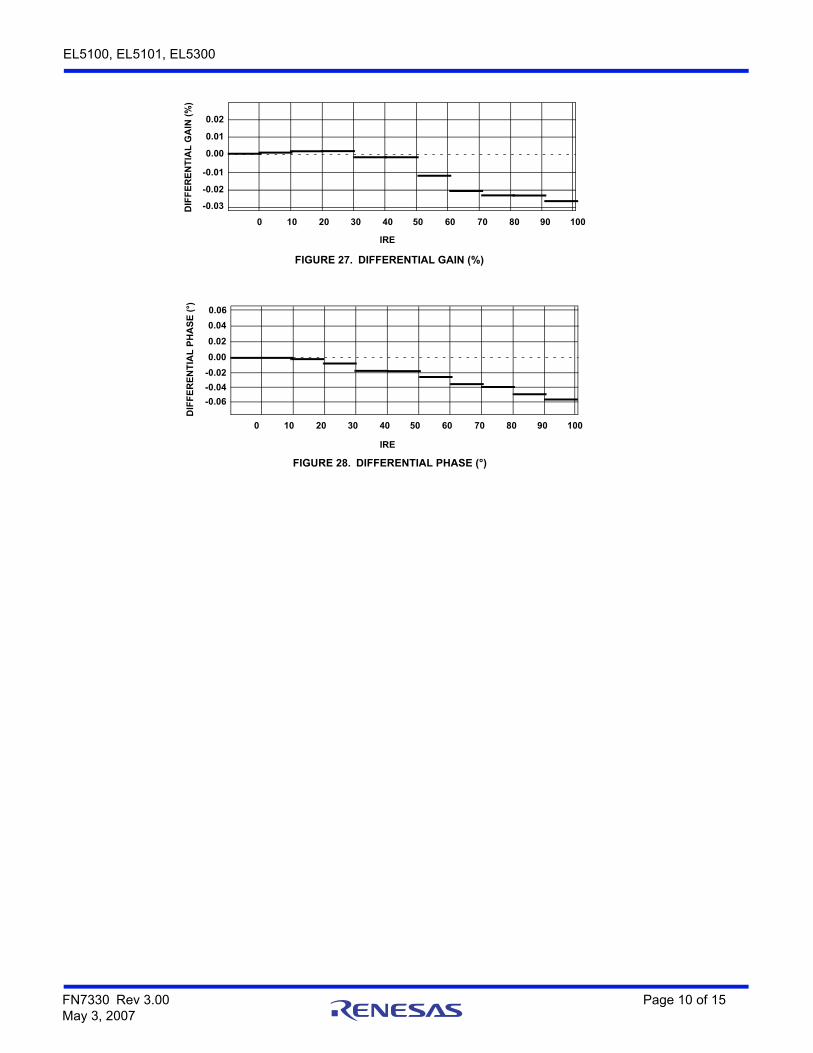
dG Differential Gain AV = 2, RL = 150, VINDC = -1 to +1V 0.08 %
dP Differential Phase AV = 2, RL = 150, VINDC = -1 to +1V 0.1 °
eN Input Noise Voltage f = 10kHz 10 nV/Hz
iN Input Noise Current f = 10kHz 7 pA/Hz
tDIS Disable Time 180 ns
tEN Enable Time 650 ns
Typical Performance Curves
FIGURE 1. GAIN vs FREQUENCY FOR VARIOUS CL FIGURE 2. GAIN vs FREQUENCY FOR VARIOUS CL
FIGURE 3. GAIN vs FREQUENCY FOR VARIOUS CIN- FIGURE 4. GAIN vs FREQUENCY FOR VARIOUS CIN-
NO
RM
AL
IZE
D G
AIN
(d
B)
5
3
1
-1
-3
-5100K 1M 100M 1G
FREQUENCY (Hz)
10M
4
2
0
-2
-4
AV=+1RL=50SUPPLY=±5.0V
±1.75
±2.0
±3.0 ±4.0±5.0
NO
RM
AL
IZE
D G
AIN
(d
B)
5
3
1
-1
-3
-5100K 1M 100M 1G
FREQUENCY (Hz)
10M
4
2
0
-2
-4
AV=+1RL=500CIN-=0pFSUPPLY=±5.0V
8.8pF
6.6pF
4.4pF
2.2pF
0pF
4
2
0
-2
-4
5
3
1
-1
-3
100K 1M 10M 600M
FREQUENCY (Hz)
100M
AV=+2RL=150CL=2.2pFRF=383
17.1pF
11.5pF
5.8pF
2.2pF
NO
RM
AL
IZE
D G
AIN
(d
B)
-5
4
2
0
-2
-4
5
3
1
-1
-3
100K 1M 10M 600M
FREQUENCY (Hz)
100M
AV=+2RF=RG=383CL=2.2pFRL=150
4.4pF
6.6pF
NO
RM
AL
IZE
D G
AIN
(d
B)
-5
2.2pF
0pF
FN7330 Rev 3.00 Page 5 of 15May 3, 2007

EL5100, EL5101, EL5300
FIGURE 5. GAIN vs FREQUENCY FOR VARIOUS CIN (-) FIGURE 6. GAIN vs FREQUENCY FOR VARIOUS RL
FIGURE 7. GAIN vs FREQUENCY FOR VARIOUS RLFIGURE 8. GAIN vs FREQUENCY FOR VARIOUS RL
FIGURE 9. GAIN vs FREQUENCY FOR VARIOUS RLFIGURE 10. EQUIVALENT INPUT VOLTAGE NOISE vs
FREQUENCY
Typical Performance Curves (Continued)N
OR
MA
LIZ
ED
GA
IN (
dB
) 4
2
0
-2
-4
5
3
1
-1
-3
100K 1M 10M
FREQUENCY (Hz)
100M-5
AV=+5RF=383CL=2.2pFRL=150
13.4pF
7.8pF
2.2pF
NO
RM
AL
IZE
D G
AIN
(d
B)
5
3
1
-1
-3
-5100K 1M 100M 1G
FREQUENCY (Hz)
10M
4
2
0
-2
-4
AV=+1RL=500CL=2.5pFCIN-=0pFSUPPLY=±5.0V
50
500
200
100
20
NO
RM
AL
IZE
D G
AIN
(d
B) 4
2
0
-2
-4
5
3
1
-1
-3
100K 1M 10M
FREQUENCY (Hz)
100M-5
AV=+5RF=383CL=2.2pFRL=150
150750
2.0
1.5
4
2
0
-2
-4
5
3
1
-1
-3
100K 1M 10M 600M
FREQUENCY (Hz)
100M
AV=+1CL=2.2pF
NO
RM
AL
IZE
D G
AIN
(d
B)
-5
1500
200
500
1000
400
4
2
0
-2
-4
5
3
1
-1
-3
100K 1M 10M 600M
FREQUENCY (Hz)
100M
AV=+2RF=RG=383CL=2.2pFRL=150
NO
RM
AL
IZE
D G
AIN
(d
B)
383
715
1.5k
-5
150
NO
ISE
VO
LR
AG
E (
nv/H
z)
100
110 100 10K 100K
FREQUENCY (Hz)
1K
10
VS=±5V
FN7330 Rev 3.00 Page 6 of 15May 3, 2007

EL5100, EL5101, EL5300
FIGURE 11. OPEN LOOP GAIN AND PHASE vs FREQUENCY FIGURE 12. ZOUT vs FREQUENCY
FIGURE 13. PSRR vs FREQUENCY FIGURE 14. CMRR vs FREQUENCY
FIGURE 15. LARGE SIGNAL RISE TIME FIGURE 16. LARGE SIGNAL FALL TIME
Typical Performance Curves (Continued)O
PE
N L
OO
P G
AIN
(d
B)
90
70
50
30
10
100
80
60
40
20
500 10K 1M 500M
FREQUENCY (Hz)
100K 100M10M0
VS=±5V
1K
PH
AS
E (
°)
36
108
180
252
0
72
144
216
PHASE
GAIN ZO
UT (
)
1
0.0110K 100K 10M 100M
FREQUENCY (Hz)
1M
0.1
VS=±5VAV=+1
10
PS
RR
(d
B)
0
-20
-40
-60
-80
10
-10
-30
-50
-70
10 100 100K 500M
FREQUENCY (Hz)
1K 100M1M-90
AV=+1VS=±5VRL=150
+VS
-VS
10K 10M
CM
RR
(d
B)
-20
-40
-60
-80
-100
-10
-30
-50
-70
-90
1K 10K 1M 500M
FREQUENCY (Hz)
100K 100M10M-110
AV=+10VS=±5V
TIME (2ns/DIV)
CH1
CH2
INPUT CH1
OUTPUT CH2
CH1=500mV/DIV 50CH2=100mV/DIV 50
CH1 RISE1.408ns
CH2 RISE1.787ns
TIME (2ns/DIV)
CH1
CH2
INPUT CH1
OUTPUT CH2
CH1=500mV/DIV 50CH2=100mV/DIV 50
CH1 FALL1.103ns
CH2 FALL1.549ns
FN7330 Rev 3.00 Page 7 of 15May 3, 2007

EL5100, EL5101, EL5300
FIGURE 17. SMALL SIGNAL RISE TIME FIGURE 18. SMALL SIGNAL RISE TIME
FIGURE 19. SMALL SIGNAL FALL TIME FIGURE 20. CURRENT NOISE
FIGURE 21. GAIN vs FREQUENCY FOR VARIOUS CL FIGURE 22. GAIN vs FREQUENCY FOR VARIOUS CL
Typical Performance Curves (Continued)
TIME (2ns/DIV)
CH1
CH2
CH1=10mV/DIVCH2=2mV/DIV
VCC VEE = 5VAV=1RL=150 INPUT CH1
OUTPUT CH2
CH1 RISE1.717ns
CH2 RISE1.808ns
TIME (2ns/DIV)
CH1
CH2
CHANNEL 1
CHANNEL 2
CH1=10mVCH2=2mV
AV=+1RL=150VS=±5V
TIME (2ns/DIV)
CH1
CH2
INPUT CH1
OUTPUT CH2
CH1=10mV/DIVCH2=2mV/DIV
VCC VEE = 5VAV=1RL=150
CH1 FALL1.306ns
CH2 FALL2.351ns
CU
RR
EN
T N
OIS
E (
pA
)
100 10K 100K
FREQUENCY (Hz)
1K
100
10
1
4
2
0
-2
-4
5
3
1
-1
-3
100K 1M 10M 600M
FREQUENCY (Hz)
100M
AV=+1RL=150
NO
RM
AL
IZE
D G
AIN
(d
B)
15pF
-5
2.2pF
7.8pF
13.4pF4
2
0
-2
-4
5
3
1
-1
-3
100K 1M 10M 600M
FREQUENCY (Hz)
100M
RL=150CIN-=0pF 24.6 pF
NO
RM
AL
IZE
D G
AIN
(d
B)
13.4pF
7.8pF
-5
19pF
2.2pF
FN7330 Rev 3.00 Page 8 of 15May 3, 2007

EL5100, EL5101, EL5300
FIGURE 23. GAIN vs FREQUENCY FOR VARIOUS CL FIGURE 24. GAIN vs FREQUENCY FOR VARIOUS CL
FIGURE 25. PACKAGE POWER DISSIPATION vs AMBIENT TEMPERATURE
FIGURE 26. PACKAGE POWER DISSIPATION vs AMBIENT TEMPERATURE
Typical Performance Curves (Continued)N
OR
MA
LIZ
ED
GA
IN (
dB
) 4
2
0
-2
-4
5
3
1
-1
-3
100K 1M 10M
FREQUENCY (Hz)
100M-5
AV=+5RF=383RL=150
72pF
50pF
38pF
2.2pF
20pF
NO
RM
AL
IZE
D G
AIN
(d
B) 4
2
0
-2
-4
5
3
1
-1
-3
100K 1M 10M
FREQUENCY (Hz)
100M-5
AV=+2RF=383RL=150CIN=0pF
50pF
44pF
38pF
26pF
7.8pF
2.2pF
1.8
0.8
0
1.6
0.4
1.2
0.2
0.6
1.4
1
JEDEC JESD51-7 HIGH EFFECTIVE THERMAL CONDUCTIVITY TEST BOARD
0
AMBIENT TEMPERATURE (°C)
PO
WE
R D
ISS
IPA
TIO
N (
W)
25 125 15075 10050 85
543mW
1.136WSO8
JA =110°C/W
SOT23-5/6JA=230°C/W
1.116W
JA=112°C/W
QSOP16
0
1.2
0.6
0
JEDEC JESD51-3 LOW EFFECTIVE THERMAL CONDUCTIVITY TEST BOARD
0
AMBIENT TEMPERATURE (°C)
PO
WE
R D
ISS
IPA
TIO
N (
W)
25 125 15075
1
0.4
0.8
0.2
10050 85
488mW
781mW
SOT23-5/6JA=256°C/W
791mW
JA=158°C/W
QSOP16
SO8JA=160°C/W
FN7330 Rev 3.00 Page 9 of 15May 3, 2007
EL5100, EL5101, EL5300
0.00
0 10
0.02
-0.01
0.01
-0.02
-0.03
20 30 40 50 60 70 80 90 100
FIGURE 27. DIFFERENTIAL GAIN (%)
DIF
FE
RE
NT
IAL
GA
IN (
%)
IRE
0.04
0 10
0.02
-0.04
0.00
-0.06
20 30 40 50 60 70 80 90 100
0.06
FIGURE 28. DIFFERENTIAL PHASE (°)
DIF
FE
RE
NT
IAL
PH
AS
E (
°)
-0.02
IRE
FN7330 Rev 3.00 Page 10 of 15May 3, 2007

EL5100, EL5101, EL5300
Application Information
Video Amplifier with Reduced Size Output Capacitance
If you have a video line driver Z = 75, the DC decoupling capacitor could be relatively large.
=
f = 10Hz, R = Z = 75, C = 132µF
By using the circuit below, C could be reduced to C2 = 22µF.
FIGURE 30. VIDEO-
The test result is shown on Figure 30.
By selecting a different value for C1, we could reduce the effect, created by C3 R3 and get flat response from 16Hz with an 1/5 value, price and size output capacitor. There is another, very important issue by using high bandwidth amplifiers.
In the past when the bandwidth of the operational amplifier ended at a few hundred kHz even at few MHz, the power-supply bypass was not a very critical issue, since a 0.1µF capacitor “did the job”, but today’s amplifiers could have bandwidth, what used to be reserved for microwave circuits not to long time ago.
Therefore that high bandwidth amplifiers require the same respect what we reserve for microwave circuits. Particularly the power supply bypass and the pcb-layout could very heavily influence the performance of a modern high bandwidth amplifiers. It could happen above a few MHz, but it will happen above 100MHz, that the capacitor will behave like an inductor.
fR2
1C
FIGURE 29.
3
26
74
-
+
U1EL5104
R1 20K
R2 20KR3 10k
R4
75
R5 500
R6 500
C2
22µF
C3
1.5µF
R7 75
C1
C
C4
1n
C5
22µF
R83R3
C6
33nF
Z = 75
Vs+
-45
-40
-35
-30
-25
-20
-15
-10
-5
0
5
10
1.00E+001.00E+01
1.00E+021.00E+03
1.00E+041.00E+05
1.00E+061.00E+07
1.00E+081.00E+09
FREQUENCY (Hz)
GA
IN (
dB
)
Conditions/comments:
(1) C1 = 1µF Vs = +10V(2) C1 = 0.47µF Vs = +10V(3) C1 = 0.47µF Vs = +5V
FN7330 Rev 3.00 Page 11 of 15May 3, 2007

EL5100, EL5101, EL5300
The reason for that is the very small but not zero value serial inductance of the capacitor.
The capacitor will behave as a capacitor up to its resonance frequency, above the resonance frequency it will behave as an inductor.
Just 1nHy inductance serial with 1nF capacitance will have serial resonance at:
C = 1nF, L = 1nHy, F = 159 MHz
And an other 1nHy is very easy to get together with the inductance of traces on the pcb, and therefore you could encounter resonances from ca 50MHz and above anywhere. So if the amplifier has a bandwidth of a few hundred MHz, the proper power supply by-pass could become a serious if not difficult task.
Intuitively, you would use capacitors value 0.1µF parallel with a few µF tantalum, and to cure the effect of it’s serial resonance put a smaller one parallel to it.
The result will surprise to you, because you will get even something worse than without the small capacitor.
What is happening there? Just look what we get:
Above its serial resonance C2* the ideal capacitance of C2 is a short, the Tantalum capacitor for high frequencies is not effective, the left over is C1 capacitor and L1 + L2 inductors, we get a parallel tank circuit, which is at it’s resonance a high impedance path and do not carry any high frequency current, it does not work as bypass at all!
The impedance of a parallel tank circuit at resonance is dependent from it’s Q. High Q high impedance.
The Q of a parallel tank circuit could be reduced by bypassing it with a resistor, or adding a resistor in serial to one of the reactive components. Since the bypassing would short the DC supply we do have to go to add resistor in serial to the reactive component, we will ad a resistor serial with the inductor. (See Figure 33.)
The final power supply bypass circuit will look:
FIGURE 31.
Ci
Li
Z
F
F RES
IND
UC
TIV
E
CA
PA
CIT
IVE
CL2
1F
C1
1n
C3
22µF
C2
0.1µF
L2L1
C1
1n
C3
22µF
C2
0.1µF =
<
FIGURE 32.
C3
0.1µF
L3
C1Z
F
F RES
R3 = 3
R3 = 0
R32 to 3
FIGURE 33.
C1
1n
C11
22µFR10
3R3
C12
33nF
Vs+
FIGURE 34.
FN7330 Rev 3.00 Page 12 of 15May 3, 2007

EL5100, EL5101, EL5300
FN7330 Rev 3.00 Page 13 of 15May 3, 2007
Small Outline Package Family (SO)
GAUGEPLANE
A2
A1 L
L1
DETAIL X
4° ±4°
SEATINGPLANE
eH
b
C
0.010 BM C A0.004 C
0.010 BM C A
B
D
(N/2)1
E1E
NN (N/2)+1
A
PIN #1I.D. MARK
h X 45°
A
SEE DETAIL “X”
c
0.010
MDP0027SMALL OUTLINE PACKAGE FAMILY (SO)
SYMBOL
INCHES
TOLERANCE NOTESSO-8 SO-14SO16
(0.150”)SO16 (0.300”)
(SOL-16)SO20
(SOL-20)SO24
(SOL-24)SO28
(SOL-28)
A 0.068 0.068 0.068 0.104 0.104 0.104 0.104 MAX -
A1 0.006 0.006 0.006 0.007 0.007 0.007 0.007 0.003 -
A2 0.057 0.057 0.057 0.092 0.092 0.092 0.092 0.002 -
b 0.017 0.017 0.017 0.017 0.017 0.017 0.017 0.003 -
c 0.009 0.009 0.009 0.011 0.011 0.011 0.011 0.001 -
D 0.193 0.341 0.390 0.406 0.504 0.606 0.704 0.004 1, 3
E 0.236 0.236 0.236 0.406 0.406 0.406 0.406 0.008 -
E1 0.154 0.154 0.154 0.295 0.295 0.295 0.295 0.004 2, 3
e 0.050 0.050 0.050 0.050 0.050 0.050 0.050 Basic -
L 0.025 0.025 0.025 0.030 0.030 0.030 0.030 0.009 -
L1 0.041 0.041 0.041 0.056 0.056 0.056 0.056 Basic -
h 0.013 0.013 0.013 0.020 0.020 0.020 0.020 Reference -
N 8 14 16 16 20 24 28 Reference -
Rev. M 2/07NOTES:
1. Plastic or metal protrusions of 0.006” maximum per side are not included.
2. Plastic interlead protrusions of 0.010” maximum per side are not included.
3. Dimensions “D” and “E1” are measured at Datum Plane “H”.
4. Dimensioning and tolerancing per ASME Y14.5M-1994

EL5100, EL5101, EL5300
FN7330 Rev 3.00 Page 14 of 15May 3, 2007
SOT-23 Package Family
e1
N
A
D
E
4
321
E1
0.15 DC
2X0.20 C
2Xe
B 0.20 M DC A-Bb
NX
6
2 3
5
SEATINGPLANE
0.10 C
NX
1 3
C
D
0.15 A-BC
2X
A2
A1
H
c
(L1)
L
0.25
0° +3°-0°
GAUGEPLANE
A
MDP0038SOT-23 PACKAGE FAMILY
SYMBOL
MILLIMETERS
TOLERANCESOT23-5 SOT23-6
A 1.45 1.45 MAX
A1 0.10 0.10 ±0.05
A2 1.14 1.14 ±0.15
b 0.40 0.40 ±0.05
c 0.14 0.14 ±0.06
D 2.90 2.90 Basic
E 2.80 2.80 Basic
E1 1.60 1.60 Basic
e 0.95 0.95 Basic
e1 1.90 1.90 Basic
L 0.45 0.45 ±0.10
L1 0.60 0.60 Reference
N 5 6 Reference
Rev. F 2/07NOTES:
1. Plastic or metal protrusions of 0.25mm maximum per side are not included.
2. Plastic interlead protrusions of 0.25mm maximum per side are not included.
3. This dimension is measured at Datum Plane “H”.
4. Dimensioning and tolerancing per ASME Y14.5M-1994.
5. Index area - Pin #1 I.D. will be located within the indicated zone (SOT23-6 only).
6. SOT23-5 version has no center lead (shown as a dashed line).

FN7330 Rev 3.00 Page 15 of 15May 3, 2007
EL5100, EL5101, EL5300
Intersil products are manufactured, assembled and tested utilizing ISO9001 quality systems as notedin the quality certifications found at www.intersil.com/en/support/qualandreliability.html
Intersil products are sold by description only. Intersil may modify the circuit design and/or specifications of products at any time without notice, provided that such modification does not, in Intersil's sole judgment, affect the form, fit or function of the product. Accordingly, the reader is cautioned to verify that datasheets are current before placing orders. Information furnished by Intersil is believed to be accurate and reliable. However, no responsibility is assumed by Intersil or its subsidiaries for its use; nor for any infringements of patents or other rights of third parties which may result from its use. No license is granted by implication or otherwise under any patent or patent rights of Intersil or its subsidiaries.
For information regarding Intersil Corporation and its products, see www.intersil.com
For additional products, see www.intersil.com/en/products.html
© Copyright Intersil Americas LLC 2004-2007. All Rights Reserved.All trademarks and registered trademarks are the property of their respective owners.
Quarter Size Outline Plastic Packages Family (QSOP)
0.010 C A B
SEATING
PLANE
DETAIL X
E E1
1 (N/2)
(N/2)+1N
PIN #1I.D. MARK
b 0.004 C
c
A
SEE DETAIL "X"
A2
4°±4°
GAUGEPLANE
0.010
LA1
D
B
H
C
e
A
0.007 C A B
L1
MDP0040QUARTER SIZE OUTLINE PLASTIC PACKAGES FAMILY
SYMBOL
INCHES
TOLERANCE NOTESQSOP16 QSOP24 QSOP28
A 0.068 0.068 0.068 Max. -
A1 0.006 0.006 0.006 ±0.002 -
A2 0.056 0.056 0.056 ±0.004 -
b 0.010 0.010 0.010 ±0.002 -
c 0.008 0.008 0.008 ±0.001 -
D 0.193 0.341 0.390 ±0.004 1, 3
E 0.236 0.236 0.236 ±0.008 -
E1 0.154 0.154 0.154 ±0.004 2, 3
e 0.025 0.025 0.025 Basic -
L 0.025 0.025 0.025 ±0.009 -
L1 0.041 0.041 0.041 Basic -
N 16 24 28 Reference -
Rev. F 2/07NOTES:
1. Plastic or metal protrusions of 0.006” maximum per side are not included.
2. Plastic interlead protrusions of 0.010” maximum per side are not included.
3. Dimensions “D” and “E1” are measured at Datum Plane “H”.
4. Dimensioning and tolerancing per ASME Y14.5M-1994.


