ELECTRICAL & COMPUTER ENGINEERING
O R E G O N S T A T E U N I V E R S I T Y
College of Engineering WAGER, John F. Professor
BIRTH DATE January 22, 1953
DEGREES B.S., Engineering Physics, Oregon State University, 1977 M.S., Electrical Engineering, Colorado State University, 1978 Ph.D., Electrical Engineering, Colorado State University, 1981 ACADEMIC POSITIONS Michael and Judith Gaulke Endowed Chair, School of EECS, Oregon State University, 2012- Professor, Department of Electrical & Computer Engr., Oregon State University, 1993- Associate Professor, Department of ECE, Oregon State University, 1989-1993 Assistant Professor, Department of ECE, Oregon State University, 1984-1989
Postdoc, Department of Electrical Engineering, Colorado State University, 1981-1982 NON-ACADEMIC POSITIONS Sabbatical Leave, Cambridge University, Fall 2009 Sabbatical Leave, Tottori University, Tottori, Japan; KIST, Seoul, Korea; ETRI, Daejeon,Korea; University of Helsinki, Helsinki, Finland, Spring 2000 Sabbatical Leave, U.S. Army Research Laboratory, Fort Monmouth, NJ, Winter-Spring 1992 Member of the Technical Staff, Hughes Research Laboratories, Malibu, CA, 1982-1984 Visiting Research Engineer, Solar Energy Research Institute, Golden, CO, 1982 Research Engineer, Naval Ocean Systems Center, San Diego, CA, 1980 FIELDS OF SPECIALIZATION Solid-state electronics Fabrication, characterization, and modeling of electronic materials and devices Transparent electronics Printed electronics Oxide electronics Metal-insulator tunneling electronics Thin-film solar cells PROFESSIONAL ACTIVITIES Professional Societies American Vacuum Society (Member) 1985 Vice Chairman, Pacific Northwest Chapter 1986 Chairman, Pacific Northwest Chapter
WAGER, John F. Professor
2
Institute of Electrical and Electronics Engineers (2012 Fellow “for contributions to the development of transparent electronics”) Society of Information Display (Member) Materials Research Society (Member) Professional Service 1986: Co-Organizer, "SILI-CON 1986," Portland International Conference and Exposition on Silicon Materials and Technology, Portland, OR, June 30-July2, 1986. 1986: Short Course Instructor, "GaAs Integrated Circuits," at SILI-CON 1986. 1987: Program Committee, "Atomic and Molecular Processing of Electronic and Ceramic Materials: Preparation, Characterization, and Properties," Seattle, WA, August 30- September 2, 1987. 1987: Short Course Instructor, "GaAs Integrated Circuits," at The Portland Conference, October 12-13, 1987. 1993-2000: Steering Committee Member, Phosphor Technology Center of Excellence. 1994: International Programme Committee, 7th International Workshop on Inorganic and Organic Electroluminescence, October 10-12, 1994, Beijing, China. 1995: Program Committee, First International Conference on the Science and Technology of Display Phosphors, November 14-16, 1995, San Diego, CA. 1996: International Programme Committee, EL 96 International Workshop on Inorganic and Organic Electroluminescence, Berlin, Germany August 13-15, 1996. 1996: International Advisory and Program Committee, International Workshop of Advanced Technologies of Multicomponent Solid Films and Structures and Their Application in Photonics, October 3-5, 1996, Uzhgorod, Ukraine. 1996-1998: Chairman, 9th International Workshop on Inorganic and Organic Electroluminescence, Bend, Oregon, September 14-17, 1998. 1999: Program Committee, Fifth International Conference on the Science and Technology of Display Phosphors, November 8-10, 1999, San Diego, CA. 1999:International Advisory Committee, 1st International Display Manufacturing Conference (IDMC 2000), Seoul, Korea, September 5-7, 2000 2000: Program Committee, Sixth International Conference on the Science and Technology of Display Phosphors, November 6-8, 2000, San Diego, CA. 2000: Program Committee, 10th International Workshop on Inorganic and Organic Electroluminescence, Hamamatsu, Japan, December 4-7, 2000. 2001: Program Committee, 1st International Conference on the Science and Technology of Emissive Displays and Lighting, November 12-14, 2001, San Diego, CA. 2002:International Advisory Committee, 2nd International Display Manufacturing Conference (IDMC 2002), Seoul, Korea, February 26-28, 2002. 2002: Program Committee, 11th International Workshop on Inorganic and Organic Electroluminescence, Ghent, Belgium, September 23-26, 2002. 2004: Program Committee, 12th International Workshop on Inorganic and Organic Electroluminescence, Toronto, Canada, September 20-23, 2004. 2006: Symposium Co-organizer, “Advances in Transparent Electronics: From Materials to Devices,” Symposium R, European Materials Research Society, International Union of Materials Research Societies, E-MRS IUMRS ICEM 2006, Nice, France, May 29 – June 2, 2006.

WAGER, John F. Professor
3
2006: International Advisory Committee, 1st International Symposium on Transparent Oxides, Heraklion, Crete, October 22-25, 2006. 2007: Symposium Co-organizer, “Advances in Transparent Electronics: From Materials to Devices II,” European Materials Research Society, E-MRS 2007 2008: Inorganic Program Committee, 14th International Workshop on Inorganic and Organic Electroluminescence, Rome, Italy September 9-12, 2008. 2008: Program Committee, The 28th International Display Research Conference, University of Central Florida, Orlando, FL, November 3-6, 2008. 2008: Symposium Co-organizer, “Transparent Conductors and Semiconductors for Optoelectronics”, Materials Research Society, Fall Meeting, Boston, MA., December 1-5, 2008 2008: International Advisory Committee, 2nd International Symposium on Transparent Oxides, Hersonissos, Crete, October 22-26, 2008. 2010: International Organizing Committee, 3rd International Symposium on Transparent Oxides, Hersonissos, Crete, October 22-26, 2010. 2010: Inorganic Program Committee, 15th International Workshop on Inorganic and Organic Electroluminescence, St. Petersburg, Russia September 2010. 2010: International Advisory Board of Symposium FH “Recent Developments in the Research and Application of Transparent Conducting and Semiconducting Oxides” of the Forum on New Materials, 12th International Ceramics Congress (CIMTEC 2010) (June 6-11, 2010) and of the 5th Forum on New Materials (June 13-18, 2010), Montecatini- Florence, Italy. 2011: International Scientific Committee, “Advances in Transparent Electronics: From Materials to Devices III”, E-MRS 2011 Fall Meeting, Warsaw, Poland, September 19 – 23, 2011. 2011: Displays Sub-committee, IEEE Photonics Society Annual Meeting (Photonics 2011), Arlington, VA, October 9-13, 2011. 2012: Inorganic Program Committee, 16th International Workshop on Inorganic and Organic Electroluminescence, Hong Kong, December 10-14, 2012. 2013: International Advisory Committee, ITC2013, 9th International Thin-Film Transistor Conference, Tokyo, Japan, March 1-2, 2013. 2013: International Advisory Committee, ICANS-25, 25th International Conference on Amorphous and Nanocrystalline Semiconductors, Toronto, Canada, August 18-23, 2013. AWARDS 1988 Loyd Carter Award Finalist (OSU College of Engineering award for outstanding and inspirational teaching) 1989 Loyd Carter Award (OSU College of Engineering award for outstanding and inspirational teaching) 1996 College of Engineering Alumni Professor Award (OSU College of Engineering Award in recognition for outstanding scholarly contributions to the College and to the University) 2000 College of Engineering Research Award (OSU College of Engineering Award for outstanding & sustained research leadership)
WAGER, John F. Professor
4
2005 ‘Top 5 Hot Talks/Cool Papers’ - “Amorphous Multicomponent Heavy Metal Cation Oxides for Transparent Thin-Film Transistor Applications,” presented at the MRS Fall Meeting, Boston, MA, November 28 – December 2, 2005. 2006 OSU 2006 Sigma Xi Researcher of the Year (Annual award to a member of the OSU research community that has contributed significantly to the advancement of his/her field of study.) 2007 College of Engineering Research Collaboration Award (OSU College of Engineering award in recognition of sustained, significant, and meritorious achievement in collaborative research and scholarship) 2012 Society for Information Display (SID) Special Recognition Award ("For his pioneering contributions to the development of oxide TFTs".) 2012 IEEE Fellow (“For contributions to the development of transparent electronics.”) 2012 Best paper of 2012 for the Journal of the Society for Information Display: J. F. Wager, K. Hoshino, E. S. Sundholm, R. E. Presley, R. Ravichandran, C. C. Knutson, D. A. Keszler, R. L. Hoffman, D. A. Mourey, and J. Robertson, “A framework for assessing amorphous oxide semiconductor thin-film transistor passivation,” J. Soc. Inf. Display 20/10, 589-595 (2012).
PATENTS
1. D. Keszler, D. Li, J. F. Wager, B. L. Clark, P. Keir, “Phosphor system,” United States patent number: 6,419,855; Filing date: September 16, 1999; Issue date: July 16, 2002.
2. J. F. Wager and D. A. Keszler, “Novel Materials for Polycrystalline Thin-Film Solar Cell Applications,” Application number: 10/517,728; Publication number: US 2005/0151131 A1; Filing date: June 10, 2003.
3. H. Q. Chiang, J. F. Wager, and R. L. Hoffman, “Transparent Thin-Film Transistor with a Zinc Tin Oxide Channel Layer,” OSU invention disclosure filed (2003).
4. H. Q. Chiang, R. L. Hoffman, N. L. DeHuff, D. Hong, and J. F. Wager, and “Transparent Thin-Film Transistor with a Zinc Indium Oxide Channel Layer,” OSU invention disclosure filed (2003).
5. R. L. Hoffman, J. F. Wager D. Hong, and H. Q. Chiang, “Passivation of oxide semiconductor channel thin-film transistors,” OSU invention disclosure filed (2004).
6. Randy Hoffman, Hai Chiang, John Wager, “Semiconductor Device,” Application number: 10/763,353; Publication number: US 2005/0017244 A1; Filing date: January 23, 2004.
7. J. F. Wager and S. H. Linn, “Photoconductor for Spatial Light Modulator Applications,” OSU invention disclosure filed (2005).
8. H. Q. Chiang, D. Hong, J. F. Wager, and D. A. Keszler, “Copper Zinc Oxide for p-channel Thin-Film Transistor Applications,” OSU invention disclosure filed (2006).
9. R. L. Hoffman and J. F. Wager, “Transistor Device having a Delafossite Material,” United States patent number: 7,026,713; Filing date: December 17, 2003; Issue date: April 11, 2006.
10. J. F. Wager and D. Hong, “Amorphous multi-component oxide insulators for oxide electronics thin-film transistor gate applications,” OSU invention disclosure (2007).
WAGER, John F. Professor
5
11. H. Q. Chiang, R. L. Hoffman, N. L. DeHuff, D. Hong, and J. F. Wager, and “Semiconductor Device,” United States patent number: 7,145,174; Filing date: Mar 12, 2004; December 5, (2006).
12. J. F. Wager, and R. L. Hoffman, “Transistor structures having a transparent channel,” United States patent number: 7,189,992; Filing date: November 27, 2002; Issue date: March 13, 2007.
13. E. William Cowell III, John F. Wager III, Brady Gibbons, Douglas A. Keszler, “Amorphous Multi-component Metallic Thin Films for Electronic Device and MEMS Applications,” OSU invention disclosure filed (2008).
14. J. F. Wager, and R. L. Hoffman, “Transistor structures,” United States patent number: 7,339,187; Filing date: January 24, 2003; Issue date: March 4, 2008.
15. Randy Hoffman, John Wager, David Hong, Hai Chiang, “Method to form a passivation layer,” United States patent number: 7,382,421; Filing date: October 12, 2004; Issue date: June 3, 2008.
16. Hai Q. Chiang, Randy L. Hoffman, David Hong, Nicole L. Dehuff, John F. Wager, “A semiconductor device can include a channel including a zinc-indium oxide film,” United States patent number: 7,629,191; Filing date: September 26, 2006; Issue date: December 8, 2009.
17. J. F. Wager, D. A. Keszler, R. E. Presley, and E. S. Sundholm, “Amorphous Materials for Oxide Electronics,” OSU invention disclosure filed (2009).
18. R. E. Presley, C. Knutson, D. A. Keszler, J. F. Wager, and R. L. Hoffman, “Multicomponent Oxide Passivation Materials for Oxide Semiconductor Thin-Film Transistors,” OSU/HP invention disclosure filed (2010).
19. E. William Cowell III, John F. Wager III, Brady Gibbons, Douglas A. Keszler, “Amorphous multi-component metallic thin films for electronic devices,” U.S. Pat. Appl. Publ. US20100777194 20100510 (2010).
20. J. F. Wager, and R. L. Hoffman, “Transistor structures and methods for making the same,” United States patent number: 7,888,207; Filing date: February 5, 2007; Issue date: February 15, 2011.
21. Douglas A. Keszler, E. William Cowell III, John F. Wager III, “Metal-Insulator-Metal Device,” OSU invention disclosure filed (2012).
22. E. William Cowell III, John F. Wager, Brady J. Gibbons, Douglas A. Keszler, “Amorphous multi-component metallic thin films for electronic devices,” United States patent number: 8,436,337 B2; Filing date: May 10, 2010; Issue date: May 7, 2013.
PUBLICATIONS Books and Book Chapters
1. J. F. Wager and C. W. Wilmsen, "The Deposited Insulator/III-V Semiconductor Interface," a chapter in Physics and Chemistry of III-V Compound Semiconductor Interfaces, Plenum, C. W. Wilmsen, Editor (1985).
2. Atomic and Molecular Processing of Electronic and Ceramic Materials, Proceedings of the Conference held August 30-September 2, 1987, University of Washington, Seattle, Washington, MRS, I. A. Aksay, G. L. McVay, T. G. Stoebe, and J. F. Wager, Editors (1987).
WAGER, John F. Professor
6
3. J. F. Wager and P. D. Keir, "Electrical Characterization of Thin-Film Electroluminescent Devices," Annual Review of Materials Science 27, 228 (1997).
4. J. C. Hitt, J. P. Bender, and, J. F. Wager, "Thin-Film Electroluminescent Device Physics Modeling," CRC Reviews in Solid State and Materials Sciences 25, 29 (2000).
5. B. A. Baukol, P. D. Keir, B. A. Cleary, C. A. Nevers, T. K. Plant, and J. F. Wager, “Electro-Optic Characterization of Thin-Film Electroluminescent Devices Handbook of Luminescence and Display Materials and Devices, edited by H. S. Nalwa and L. S. Rohwer, American Scientific Publishers, 385-412 (2003).
6. J. F. Wager, D. A. Keszler, and R. E. Presley, “Transparent Electronics”, Springer (2008).
7. D. Hong, G, Yerubandi, H. Q. Chiang, M. Spiegelberg, and J. F. Wager, “Electrical Modeling of Thin-Film Transistors,” Critical Reviews in Solid State and Materials Sciences 33, 101-132 (2008).
8. J. F. Wager and B. Yeh, “Oxide Thin-Film Transistors: Device Physics,” in Bengt G. Svensson, Stephen J. Pearton, and Chennupati Jagadish; editors: Semiconductors, Semiconductors and Semimetals, Vol. 88, Burlington: Academic Press, 283-315 (2013).
Technical Journals 1. J. F. Wager and C. W. Wilmsen, "Auger Analysis of Ultrathin Si02 Layers on Silicon,"
Journal of Applied Physics 50, 874 (1979). 2. J. Shewchun, J. DuBow, C. W. Wilmsen, R. Singh, D. Burk, and J. F. Wager, "Operation
of the Semiconductor-Insulator-Semiconductor Solar Cell: Experiment," Journal of Applied Physics 50, 2832 (1979).
3. J. F. Wager and C. W. Wilmsen, "Detection of SiO2 at the Indium Tin Oxide/Si Solar Cell Interface," Journal of Applied Physics 50, 4172 (1979).
4. C. W. Wilmsen, R. W. Kee, J. F. Wager, J. Stannard, and L. Messick, "Deposited Insulator Layer/GaAs and InP Interface Formation," Thin Solid Films 64, 49 (1979).
5. H. Birey, S. J. Pak, J. R. Sites, and J. F. Wager, "Ion Beam Sputtered Al0xNy Encapsulating Films," J. Vac. Sci. Technol. 16, 2086, (1979).
6. S. M. Goodnick, J. F. Wager, and C. W. Wilmsen, "Thermal Degradation of Indium-Tin-Oxide/p-Silicon Solar Cells," J. Appl. Phys. 51, 527 (1980).
7. J. F. Wager and C. W. Wilmsen, "Thermal Oxidation of InP," J. Appl. Phys. 51, 812 (1980).
8. J. F. Wager and C. W. Wilmsen, "Si02/InP Interface Formation: Thermodynamic Consid-erations," J. Vac. Sci. Technol. 17, 800 (1980).
9. J. F. Wager, D. L. Ellsworth, S. M. Goodnick, and C. W. Wilmsen, "Composition and Thermal Stability of Thin Native Oxides on InP," J. Vac. Sci. Technol. 19, 513 (1981).
10. J. F. Wager and C. W. Wilmsen, "The Plasma-Enhanced CVD Si02/InP Interface," J. Vac. Sci. Technol. 53, 5789 (1982).
11. J. F. Wager, W. H. Makky, C. W. Wilmsen, and L. G. Meiners, "Oxidation of InP in a Plasma-Enhanced Chemical Vapor Deposition Reactor," Thin Solid Films 95, 343 (1982).
12. J. F. Wager, C. W. Wilmsen, and L. L. Kazmerski, "Estimation of the Bandgap of InPO4," Appl. Phys. Lett. 42, 589 (1983).
13. J. F. Wager, O. Jamjoum, and L. L. Kazmerski, "The CdS/CuInSe2 Solar Cell Interface: Thermodynamic Considerations," Solar Cells 9, 159 (1983).
WAGER, John F. Professor
7
14. J. F. Wager, K. M. Geib, C. W. Wilmsen, and L. L. Kazmerski, "Native Oxide Formation and Electrical Instabilities at the Insulator/InP Interface," J. Vac. Sci. Technol. B1, 778 (1983).
15. C. W. Wilmsen, J. F. Wager, K. M. Geib, T. Hwang, and M. Fathipour, "Traps at the Depo-sited Insulator-InP Interface: A Discussion of a Possible Cause," Thin Solid Films 103, 47 (1983).
16. L. L. Kazmerski, I. Jamjoum, J. F. Wager, P. J. Ireland, and K. J. Bachmann, "Summary Abstract: Oxidation of CuInSe2," J. Vac. Sci. Technol. A1, 668 (1983).
17. P. J. Ireland, O. Jamjoum, L. L. Kazmerski, R. K. Ahrenkiel, P. E. Russell, W. Stanchina, and J. F. Wager, "Surface and Interface Analysis of GaAs-oxyfluorides," J. Vac. Sci. Technol. A1, 653 (1983).
18. J. F. Wager, M. D. Clark, and R. A. Jullens, "Si02/InP Interfaces with Reduced Interface State Density," J. Vac. Sci. Technol. B2, 584 (1984).
19. K. M. Geib, S. M. Goodnick, D. Y. Lin, R. G. Gann, C. W. Wilmsen, and J. F. Wager, "Influence of Interfacial Structure of the Electronic Properties of Si02/InP," J. Vac. Sci. Technol. B2, 516 (1984).
20. J. F. Wager and D. R. Rhiger, "Surface Characterization of HgCdTe Native Oxides," J. Vac. Sci. Technol. A3, 212 (1985).
21. J. A. Van Vechten and J. F. Wager, "Consequences of Anion Vacancy Nearest Neighbor Hopping in III-V Compound Semiconductors; Drift in InP MISFET's," J. Appl. Phys. 57, 1956 (1985).
22. Z. Liliental, O. Krivanek, J. F. Wager, and S. M. Goodnick, "The Structure of the InP/SiO2 Interface," Appl. Phys. Lett. 46, 889 (1985).
23. O. Krivanek, Z. Liliental, J. F. Wager, R. G. Gann, S. M. Goodnick, and C. W. Wilmsen, "A Combined HREM, XPS, and Electrical Properties Study of the InP-SiO2 Interface," J. Vac. Sci. Technol. B3, 1081 (1985).
24. J. F. Wager and J. A. Van Vechten, "An Atomic Model for the M Center in InP," Phys. Rev. B32, 5251 (1985).
25. J. A. Van Vechten and J. F. Wager, "Asymmetry of Anion and Cation Vacancy Migration Enthalpies in III-V Semiconductors; Role of Kinetic Energy," Phys. Rev. B32, 5259 (1985).
26. B. Rastegar and J. F. Wager, "Surface Recombination Velocity and Bulk Lifetime in GaAs and InP," Semicond. Sci. Technol. 1, 207 (1986).
27. J. F. Wager, S. J. T. Owen, and S. J. Prasad, "InP MISFET Technology," J. Electrochem. Soc. 134, 160 (1987).
28. J. F. Wager and J. A. Van Vechten, "Atomic Model for EL2 in GaAs," Phys. Rev. B35, 2330 (1987).
29. J. F. Wager and A. J. McCamant, "GaAs MESFET Interface Considerations," IEEE Trans. Electron Devices ED-34, 1001 (1987).
30. J. F. Wager and J. A. Van Vechten, "Atomic Model for the ELO Defect in GaAs," J. Appl. Phys. 62, 4192 (1987).
31. M. T. Juang, J. F. Wager, and J. A. Van Vechten, "Phosphorous Vacancy Nearest-Neighbor Hopping Induced Instabilities in InP Capacitors," J. Electrochem. Soc. 135, 2019 (1987).
WAGER, John F. Professor
8
32. M. T. Juang, J. F. Wager, and J. A. Van Vechten, "Phosphorous Vacancy Nearest-Neighbor Hopping Induced Instabilities in InP Capacitors, Part II: Computer Simulation," J. Electrochem. Soc. 135, 2023 (1987).
33. J. F. Wager and J. A. Van Vechten, "Reply to "Comment on 'Atomic Model for the EL2 Defect in GaAs,'" Phys. Rev. B38, 10956 (1988).
34. S. B. Kim and J. F. Wager, "Electroluminescence in Diamond-Like Carbon Films," Appl. Phys. Lett. 53, 1880 (1988).
35. T. W. Dobson, J. F. Wager, and J. A. Van Vechten, "Entropy of Migration for Atomic Hopping," Phys. Rev. B40, 2962 (1989).
36. J. F. Wager and J. A. Van Vechten, "Reply to "Comment on 'Atomic Model for the EL2 Defect in GaAs,'" Phys. Rev. B39, 1967 (1989).
37. A. J. Nelson, D. K. Benson, C. E. Tracy, L. L. Kazmerski, and J. F. Wager, "Electron Energy-Loss Spectroscopy Analysis of Low-Temperature Plasma-Enhanced Chemically Vapor Deposited a-C:H Films," J. Vac. Sci. Technol. A7, 1350 (1989).
38. T. W. Dobson and J. F. Wager, "Enthalpy of Formation of Antisite Defects and Antistructure Pairs in III-V Compound Semiconductors," J. Appl. Phys. 66, 1997 (1989).
39. T. W. Dobson, L. V. A. Scalvi, and J. F. Wager, "Transient Decay of Persistent Photoconductivity in Al0.3Ga0.7As," J. Appl. Phys. 68, 601 (1990).
40. R. C. McArthur, J. D. Davidson, J. F. Wager, I. Khormaei, and C.N. King, "Capacitance-Voltage Characteristics of AC Thin Film Electroluminescent Devices," Appl. Phys. Lett. 56, 1889 (1990).
41. S. B. Kim, J. F. Wager, and D. C. Morton, "Short Wavelength Electroluminescence in Diamond-Like Carbon Thin Films," Thin Solid Films 189, 45 (1990).
42. S. B. Kim, J. F. Wager, and D. C. Morton, "Diamond-Like Carbon for Electroluminescent Applications," Surface and Coatings Technology 43/44, 99 (1990).
43. J. F. Wager, "A Statistical Thermodynamic Derivation of the Ballistic Model for Vacancy Migration," Phil. Mag. A 63, 1315 (1991).
44. J. F. Wager, "Energetics of Self-Diffusion in GaAs," J. Appl. Phys. 69, 3022 (1991). 45. J. D. Davidson, J. F. Wager, I. Khormaei, C. N. King, and R. Williams, "Electrical
Characterization and Modeling of Alternating-Current Thin-Film Electroluminescent Devices," IEEE Trans. Electron Devices ED-39, 1122 (1992).
46. J. D. Davidson, J. F. Wager, and S. Kobayashi, "Aging Studies of ZnS:Mn Alternating-Current Thin-Film Electroluminescent Devices," J. Appl. Phys. 71, 4040 (1992).
47. J. F. Wager, "Thermodynamics and Kinetics of Vacancy Self-Compensation in Wide Band Gap Semiconductors," Phil. Mag. A 67, 897 (1993).
48. A. A. Douglas, J. F. Wager, D. C. Morton, J.B. Koh, and C.P. Hogh, "Evidence for Space Charge in Atomic Layer Epitaxy ZnS:Mn Alternating-Current Thin-Film Electroluminescent Devices," J. Appl. Phys. 73, 293 (1993).
49. A. Abu-Dayah, S. Kobayashi, and J. F. Wager, "Internal Charge-Phosphor Field Characteristics of Alternating-Current Thin-Film Electroluminescent Devices," Appl. Phys. Lett. 62, 744 (1993).
50. K. Bhattacharyya, S. M. Goodnick, and J. F. Wager, "Monte Carlo Simulation of Electron Transport in Alternating-Current Thin-Film Electroluminescent Devices," J. Appl. Phys. 73, 3390 (1993).
WAGER, John F. Professor
9
51. A. A. Douglas, J. F. Wager, D. C. Morton, J. B. Koh, and C. P. Hogh, "Hot Electron Luminescence in ZnS Alternating-Current Thin-Film Electroluminescent Devices," Appl. Phys. Lett. 63, 231 (1993).
52. A. Abu-Dayah, J. F. Wager, and S. Kobayashi, "Electrical Characterization of Atomic Layer Epitaxy ZnS:Mn Alternating-Current Thin-Film Electroluminescent Devices Subject to Various Waveforms," J. Appl. Phys. 74, 5575 (1993).
53. A. Abu-Dayah and J. F. Wager, "Aging Studies of Atomic Layer Epitaxy ZnS:Mn Alternating-Current Thin-Film Electroluminescent Devices," J. Appl. Phys. 75, 3593 (1994).
54. S. Lim, J. H. Ryu, J. F. Wager, and T. K. Plant, "Rugate Filters Grown by Plasma-Enhanced Chemical Vapor Deposition," Thin Solid Films 245, 141 (1994).
55. S. Lim, J. H. Ryu, J. F. Wager, and L. M. Casas, "Inhomogeneous Dielectrics Grown by Plasma-Enhanced Chemical Vapor Deposition," Thin Solid Films 236, 64, 1994.
56. J. H. Ryu, S. Lim, and J. F. Wager, "Alternating-Current Thin-Film Electroluminescent Devices with Multiple Dielectric Layers," Thin Solid Films 248, 63, 1994.
57. W. M. Ang, S. Pennathur, L. Pham, J. F. Wager, S. M. Goodnick, and A. A. Douglas, "Evidence for Band-to-Band Impact Ionization in Evaporated ZnS:Mn Alternating-Current Thin-Film Electroluminescent Devices," J. Appl. Phys. 77, 2719 (1995).
58. K. Streicher, T. K. Plant, and J. F. Wager, "Hot Electron Impact Excitation of ZnS:Tb Alternating-Current Thin-Film Electroluminescent Devices," J. Appl. Phys. 78, 2101 (1995).
59. P. D. Keir, W.M. Ang, and J.F. Wager, "Modeling Space Charge in Alternating-Current Thin-Film Electroluminescent Devices using a Single Sheet Charge Model," J. Appl. Phys. 78, 4668 (1995).
60. S. Shih, P. D. Keir, and J. F. Wager, J. Viljanen "Space Charge Generation in Atomic Layer Epitaxy ZnS:Mn Alternating-Current Thin-Film Electroluminescent Devices with Varying Phosphor Layer Thickness," J. Appl. Phys. 78, 5775 (1995).
61. S. Lim, S. Shih, and J. F. Wager, "Design and Fabrication of a Double Bandstop Rugate Filter Grown by Plasma-Enhanced Chemical Vapor Deposition," Thin Solid Films 277, 144 (1996).
62. S. Shih, P. D. Keir, J. Hitt, and J. F. Wager, "On the Nature of Offset of the Charge-Voltage or Internal Charge-Phosphor Field Characteristics of Alternating-Current Thin-Film Electroluminescent Devices, " Appl. Phys. Lett. 69, 1921 (1996).
63. P. D. Keir, H. Le, R. L. Thuemler, J. Hitt, and J. F. Wager, "Relaxation Charge Anomalies in the Charge-Voltage Characteristics of Alternating-Current Thin-Film Electroluminescent Devices ", Appl. Phys. Lett. 69, 2421 (1996).
64. M. Reigrotzki, R. Redmer, I. Lee, S. S. Pennathur, J. F. Wager, S. M. Goodnick, P. Vogl, H. Eckstein, and W. Schattke, "Impact Ionization Rate and High Field Transport in ZnS with Nonlocal Band Structure," J. Appl. Phys. 80, 5054 (1996).
65. K. Lite, R. L. Thuemler, T. K. Plant, J. F. Wager, D. C. Morton, S. S. Sun, and R. H. Mauch, "Vacuum Ultraviolet Reflectivity Measurements of Thin-Film Electroluminescent Phosphors," Appl. Phys. Lett. 69, 3525 (1996).
66. I. Lee, S. Pennathur, S.M. Goodnick and J.F. Wager, "Band Structure and High-Field Transport of a ZnS Phosphor in AC Thin-Film Electroluminescent Devices," J. Korean Phys. Soc. 31, 517 (1997).
WAGER, John F. Professor
10
67. R. Myers and J. F. Wager, "Transferred Charge Analysis of Evaporated ZnS:Mn Alternating-Current Thin-Film Electroluminescent Devices," J. Appl. Phys. 81, 506 (1997).
68. J. C. Hitt, J. F. Wager, and S. S. Sun, "Static Space Charge in Evaporated ZnS:Mn Alternating-Current Thin-Film Electroluminescent Devices," J. Appl. Phys. 83, 1141 (1998).
69. M. Dur, S. M. Goodnick, S. Pennathur, J. F. Wager, M. Reigrotzki, and R. Redmer, "High-Field Transport and Electroluminescence in ZnS Phosphor Layers," J. Appl. Phys. 83, 3176 (1998).
70. J. F. Wager, Book Review, “The Mathematica Handbook,” Materials Research Bulletin 33, 1726 (1998).
71. P. D. Keir, J. F. Wager, B. L. Clark, D. Li, and D. A. Keszler, "Alkali Metal Coactivators in SrS:Cu,F Thin-Film Electroluminescent Devices," Appl. Phys. Lett. 75, 1398 (1999).
72. P. D. Keir, C. Maddix, B. A. Baukol, J. F. Wager, B. L. Clark, and D. A. Keszler, "Lanthanide Doping in ZnS and SrS Thin-Film Electroluminescent Devices," J. Appl. Phys. 86, 6810 (1999).
73. A. S. Grudzinsky, P. D. Keir, and J. F. Wager, “Simulations of SrS:Ce ACTFEL Devices Using a Two-Sheet Space Charge Model,” Display and Imaging 8, 61 (1999).
74. B. A. Baukol, J. C. Hitt, P. D. Keir, and J. F. Wager, “Electroluminescence Thermal Quenching in Thin-Film Electroluminescent Devices," Appl. Phys. Lett. 76, 185 (2000).
75. D. Li, B. L. Clark, D. A. Keszler, P. D. Keir and J. F. Wager, “Color Control in Sulfide Phosphors; Tuning Up the Light for Electroluminescent Displays," Chem. Mater. 12, 268 (2000).
76. J. P. Bender and J. F. Wager, "Alternating-Current Thin-Film Electroluminescent Device Modeling via SPICE Fowler-Nordheim Diode,” IEEE Trans. Electron Devices ED-47, 1113-1115 (2000).
77. B. A. Cleary, J.C. Hitt, P. D. Keir, T.K. Plant, J. F. Wager, and S. S. Sun, "Photo-Induced Charge and Luminescence Measurements of Evaporated ZnS:Mn Alternating-Current Thin-Film Electroluminescent Devices," J. SID Suppl. 1, 51 (2000).
78. S. S. Lee, S. Lim, S. Sun, and J. F. Wager, “A New CaSiN2 Phosphor for Thin-Film Electroluminescent Device Application,” J. SID Suppl. 1, 51 (2000).
79. B. J. Norris and J. F. Wager, “Transient Brightness, Current, and Voltage Characterization of Organic Light Emitting Devices,” J. Vac. Sci. Technol. B 19, 546-550 (2001).
80. B. A. Baukol, J. C. Hitt, J. F. Wager, and S.-S. Sun, “Electroluminescence Thermal Quenching in Alternating-Current Thin-Film Electroluminescent Devices," J. Appl. Phys. 90, 2185-2190 (2001).
81. J. C. Hitt and J. F. Wager, “Insulator Issues in Alternating-Current Thin-Film Electroluminescent Devices," J. Appl. Phys. 90, 2711-2717 (2001).
82. R. L. Hoffman, J. F. Wager, M. K. Jayaraj, and J. Tate, “Electrical Characterization of Transparent p-i-n Heterojunction Diodes," J. Appl. Phys. 90, 5763-5767 (2001).
83. J. F. Wager, J. C. Hitt, B. A. Baukol, J. P. Bender, and D. A. Keszler, “Luminescent Impurity Doping Trends in Alternating-Current Thin-Film Electroluminescent Phosphors," J. Lumin. 97, 68-81 (2002).
84. S. Park, D. A. Keszler, M. M. Valencia, R. L. Hoffman, and J. F. Wager, “p-Type BaCu2S2 Films,” Appl. Phys. Lett. 80, 4393-4394 (2002).
WAGER, John F. Professor
11
85. S. Park, B. L. Clark, D. A. Keszler, J. P. Bender, J. F. Wager, T. A. Reynolds, and G. Herman, “Low-Temperature Thin-Film Deposition and Crystallization,” Science 297, 65 (2002).
86. J. Tate, M. K. Jayaraj, A. D. Draeske, T. Ulbrich, A. W. Sleight, K. A. Vanaja, R. Ragarajan, J. F. Wager and R. L. Hoffman, “p-Type Oxides for use in Transparent Diodes," Thin Solid Films 411, 119-124 (2002).
87. B. A. Cleary, P. D. Keir, J. C. Hitt, T. K. Plant, J. F. Wager, B. Aitchison, R. T. Tuenge, and S. S. Sun, "Subthreshold Voltage-Induced Transferred Charge Measurements of Evaporated ZnS:Mn Alternating-Current Thin-Film Electroluminescent Devices," J. Soc. Info. Display 10, 271-281 (2002).
88. J. P. Bender, J. F. Wager, J. Kissick, B. L. Clark, and D. A. Keszler, “Zn2GeO4:Mn Alternating-Current Thin-Film Electroluminescent Devices,” J. Lumin. 99, 311-324 (2002).
89. R. L. Hoffman, B. J. Norris, and J. F. Wager, “ZnO-Based Transparent Thin-Film Transistors,” Appl. Phys. Lett. 82, 733-735 (2003).
90. J. F. Wager, “Transparent Electronics,” Science 300, 1245-1246 (2003). 91. R. L. Hoffman and J. F. Wager, “Energy Band Alignment of Injector / Insulator
Heterojunctions,” Thin Solid Films 436, 286-291 (2003). 92. B. J. Norris, J. Anderson, J. F. Wager, and D. A. Keszler, “Spin-Coated Zinc Oxide
Transparent Transistors,” J. Phys. D. 36, L105-L107 (2003). 93. R. E. Presley, C. L. Munsee, C.-H. Park, D. Hong, J. F. Wager, and D. A. Keszler,
“Transparent Tin Oxide Thin-Film Transistors,” J. Phys. D. 37, 2810-2813 (2004). 94. H. Q. Chiang, R. L. Hoffman, J.-Y. Jeong, J. F. Wager, and D. A. Keszler, “High Mobility
Transparent Thin-film Transistors with a Zinc Tin Oxide Channel Layer,” Appl. Phys. Lett. 86, 013503-013505 (2005).
95. C. Munasinghe, J. Heikenfeld, R. Dorey, R. Whatmore, J. P. Bender, J. F. Wager, and A. J. Steckl, “High brightness ZnS and GaN electroluminescent devices using PZT thick dielectric layers,” IEEE Trans. Electron Dev. ED-52, 194-203 (2005).
96. N. L. DeHuff, E. S. Kettenring, D. Hong, C.-H. Park, H. Q. Chiang, R. L. Hoffman, and J. F. Wager, and D. A. Keszler, “Transparent Thin-Film Transistor with a Zinc Indium Oxide Channel Layer,” J. Appl. Phys. 97, 064505:1-5 (2005).
97. D. Hong and J. F. Wager, “Passivation of Zinc Tin Oxide Thin-Film Transistors,” J. Vac. Sci. Technol. B 23, L25-L27 (2005).
98. Y. –J. Chang, C. L. Munsee, G. S. Herman, J. F. Wager, P. Mugdur, D. –H. Lee, and C. –H. Chang, “Growth, characterization and application of CdS thin films deposited by chemical bath deposition,” Surface and Interface Analysis 37, 398-405 (2005).
99. R. E. Presley, D. Hong, H. Q. Chiang, C. M. Hung, R. L. Hoffman, and J. F. Wager, “Transparent Ring Oscillator based on Indium Gallium Oxide Thin-Film Transistors,” Solid-State Electron. 50, 500-503. (2006).
100. D. Hong, H. Q. Chiang, R. E. Presley, N. L. Dehuff, J. P. Bender, C.-H. Park, J. F. Wager, D. A. Keszler, “Transparent Thin-Film Transistor Exploratory Development via Sequential Layer Deposition and Thermal Annealing,” Thin Solid Films 515, 2717-2721 (2006).
101. D. Hong, C. Q. Chiang, J. F. Wager, “Zinc Tin Oxide Thin-Film Transistors via Reactive Sputtering using a Metal Target,” J. Vac. Sci. Technol. B 24, L23-L25 (2006).
WAGER, John F. Professor
12
102. H. Q. Chiang, D. Hong, C. M. Hung, R. E. Presley, J. F. Wager, C.-H. Park, D. A. Keszler, and G. S. Herman, “Thin-film Transistors with Amorphous Indium Gallium Oxide Channel Layers,” J. Vac. Sci. Technol. B 24, 2702-2705 (2006).
103. M. S. Grover, P. A. Hersh, H. Q. Chiang, E. S. Kettenring, J. F. Wager, and D. A. Keszler, “Thin-film transistors with transparent amorphous zinc indium tin oxide channel layer,” J. Physics D 40, 1335-1338 (2007).
104. S. T. Meyers, J. T. Anderson, D. Hong, C. M. Hung, J. F. Wager, D. A. Keszler, “Solution-processed aluminum oxide phosphate thin-film dielectrics,” Chem. Of Mater.19, 4023-4029 (2007).
105. J. T. Anderson, C. L. Munsee, C. M. Hung, T. M. Phung, G. S. Herman, D. C. Johnson, J. F. Wager, and D. A. Keszler, “Solution-processed HafSOx and ZircSOx inorganic thin-film dielectrics and nanolaminates,” Adv. Funct. Mater. 17, 2117-2124 (2007).
106. J.F. Wager, “Transparent electronics: Schottky barrier and heterojunction considerations,” Thin Solid Films 516, 1755-1764 (2008).
107. P. T. Erslev, H. Q. Chiang, D. Hong, J. F. Wager, and J. D. Cohen, “Electronic properties of amorphous zinc tin oxide films by junction capacitance methods,” J. Non-Crystalline Solids 354, 2801-2804 (2008).
108. H. Q. Chiang, B. R. McFarlane, D. Hong, R. E. Presley, and J. F. Wager, “Processing effects on the stability of amorphous indium gallium zinc oxide thin-film transistors,” J. Non-Crystalline Solids 354, 2826-2830 (2008).
109. J. F. Wager, "A simple procedure for phosphor assessment," J. Lumin. 128, 1851-1855 (2008).
110. S. T. Meyers, J. T. Anderson, C. M. Hung, J. Thompson, J. F. Wager, and D. A. Keszler, “Aqueous inorganic inks for low-temperature fabrication of ZnO TFTs,” J. Am. Chem. Soc. 130, 17603-17609 (2008).
111. D. P. Heineck, B. R. McFarlane, and J. F. Wager, “Zinc tin oxide thin-film transistor enhancement/depletion inverter,” IEEE Electron Device Lett., 30, 514-516 (2009).
112. J. A. Spies, R. Schafer, J. F. Wager, P. Hersh, H. A. S. Platt, D. A. Keszler, G. Schneider, R. Kykyneshi, J. Tate, X. Liu, A. D. Compaan, W. N. Shafarman, “pin double-heterojunction thin-film solar cell p-layer assessment,” Solar Energy Materials & Solar Cells 93, 1296-1308 (2009).
113. K. Hoshino, D. Hong, H. Q. Chiang, and J. F. Wager, “Constant-voltage bias-stress testing of a-IGZO thin-film transistors,” IEEE Trans. Electron Devices 56, 1365-1370 (2009).
114. P. T. Erslev, E. Sundholm, R. E. Presley, D. Hong, J. F. Wager, and J. D. Cohen, “Mapping out the distribution of electronic states in the mobility gap of amorphous zinc tin oxide,” Appl. Phys. Lett. 95, 192115/1-192115/3 (2009).
115. B. R. McFarlane, P. Kurahashi, D. P. Heineck, R. E. Presley, E. Sundholm, and J. F. Wager, “Indium Gallium Oxide and Zinc Tin Oxide Thin-Film Transistor AC/DC Rectifiers,” IEEE Electron Device Lett. 31, 314-316 (2010).
116. K. Hoshino and J. F. Wager, “Operating temperature trends in amorphous In-Ga-Zn-O thin-film transistors,” IEEE Trans. Electron Devices 31, 818-820 (2010).
117. J. Triska, J. F. Conley, Jr. R. Presley, J. F. Wager, “Bias stress stability of zinc-tin-oxide thin-film transistors with Al2O3 gate dielectrics,” J. Vac. Sci. Technol. B 28, C5I1-C5I6. (2010).
WAGER, John F. Professor
13
118. E. W. Cowell III, C. C. Knutson, J. F. Wager, and D. A. Keszler, “Amorphous Metal/Oxide Nanolaminate,” ACS Appl. Materials & Interfaces 2, 1811-1813 (2010).
119. J. F. Wager, Invited Paper for a special issue on Oxide TFT Device and Array Technologies, “Transfer curve assessment of oxide thin-film transistors,” J. SID 18, 749-752 (2010).
120. E. W. Cowell III, N. Alimardani, C. C. Knutson, J. C. Conley, Jr., B. J. Gibbons, D. A. Keszler, and J. F. Wager, “Advancing MIM electronics: amorphous metal contacts,” Advanced Materials 23, 74-78 (2011).
121. K. Jiang, J. T. Anderson, K. Hoshino, D. Li, J. F. Wager, and D. A. Keszler, “Low-energy path to dense HfO2 thin films with aqueous precursor,” Chem. Mater. 23, 945-952 (2011).
122. J. F. Wager and R. L. Hoffman, “Thin, Fast, and Flexible: amorphous oxide semiconductors promise to makes flat-panel displays faster and sharper than today’s silicon standby,” IEEE Spectrum, May issue, pp. 42-45, 51-56 (2011).
123. J. F. Wager and J. Robertson, “Metal-induced gap states modeling of metal-Ge contacts with and without a silicon nitride ultrathin interfacial layer,” J. Appl. Phys. 109, 094501 (2011).
124. T. Waggoner, J. Triska, K. Hoshino, J. F. Wager, and J. F. Conley, Jr., “Zirconium oxide-aluminum oxide nanolaminate gate dielectrics for amorphous oxide semiconductor thin-film transistors,” J. Vac. Sci. Technol. B 29, 04D115 (2011).
125. B. D. Pelatt, R. Ravichandran, J. F. Wager, and D. A. Keszler, “Atomic solid state energy scale,” J. Am. Chem. Soc. 133, 16852-16860 (2011).
126. L. Yu, S. Lany, R. Kykyneshi, V. Jieratum, R. Ravichandran, B. Pelatt, E. Altschul, H. A. S. Platt, J. F. Wager, D. A. Keszler, and A. Zunger, “Iron Chalcogenide Photovoltaic Absorbers,” Adv. Energy Mater. 1, 748-753 (2011).
127. N. Alimardani, E. W. Cowell III, J. F. Wager, J. F. Conley, Jr., D. Evans, M. Chin, S. J. Kilpatrick, and M. Dubey, “Impact of electrode roughness on metal-insulator-metal tunnel diodes,” J. Vac. Sci. Technol. A 30, 01A113 (2012).
128. E. W. Cowell, C. C. Knutson, N. A. Kuhta, W. Stickle, D. A. Keszler, and J. F. Wager, “Engineering Anisotropic Dielectric Response Through Amorphous Laminate Structures,” Physica Status Solidi a 209, 777-784 (2012).
129. S. Lany, A. Zakutayev, T. O. Mason, J. F. Wager, K. R. Poeppelmeier, J. D. Perkins, J. J. Berry, D. S. Ginley, and A. Zunger, “Surface donors cause high conductivities in transparent oxide thin-films,” Phys. Rev. Lett. 108, 016802 (2012).
130. E. S. Sundholm, R. L. Hoffman, D. A. Mourey, C. C. Knutson, R. E. Presley, D. A. Keszler, and J. F. Wager, “Passivation of zinc tin oxide utilizing a zinc tin silicon oxide barrier layer,” IEEE Electron Device Lett. 33, 836-838 (2012).
131. J. F. Wager, K. Hoshino, E. S. Sundholm, R. E. Presley, R. Ravichandran, C. C. Knutson, D. A. Keszler, R. L. Hoffman, D. A. Mourey, and J. Robertson, “A framework for assessing amorphous oxide semiconductor thin-film transistor passivation,” J. Soc. Inf. Display 20/10, 589-595 (2012). [This paper was awarded the best paper of 2012 for the Journal of Information Display.]
132. V. Itthibenchapong, R. S. Kokenyesi, A. J. Ritenour, L. N. Zakharov, S. W. Boettcher, J. F. Wager, and D. A. Keszler, “Earth-abundant Cu-based chalcogenide semiconductors as photovoltaic absorbers,” J. Mater. Chem. C 1, 657-662 (2013).
WAGER, John F. Professor
14
133. J. F. Wager, B. Yeh, R. L. Hoffman, and D. A. Keszler, “An amorphous oxide semiconductor thin-film transistor approach to oxide electronics,” J. Curr. Opin. Solid State Mater. Sci. (2014). http://dx.doi.org/10.1016/j.cossms.2013.07.002
134. N. Alimardani, J. McGlone J. F. Wager, and J. F. Conley, Jr., “Conduction processes in metal-insulator-metal diodes with Ta2O5 and Nb2O5 insulators deposited by atomic layer deposition,” J. Vac. Sci. Technol. A (in press).
135. K. Hoshino, B. Yeh, and J. F. Wager, “Impact of humidity on the electrical performance of amorphous oxide semiconductor thin-film transistors,” J. SID (in press).
136. V. Jieratum, L. Yu, R. Kykyneshi, B. Waters, A. Zunger, J. F. Wager, and D. A. Keszler, “Cu3PX4 (X = S, Se) as Solar Absorbers,” (in preparation).
137. C. C. Knutson, R. E. Presley, R. Ravichandran, R. S. Kokenyesi, E. S. Sundholm, B. Yeh, W. Stickle, R. L. Hoffman, D. A. Mourey, J. F. Wager, J. Robertson, D. A. Keszler, “Sputter-coated Passivation of Zinc Tin Oxide,” Appl. Mater. & Interfaces (in preparation)
138. J. Heo, D. A. Keszler, R. Ravichandran, J. F. Wager, “Design meets nature: new tetrahedrite solar absorbers,” Adv. Energy Mater. (in preparation)
139. K. Hoshino and J. F. Wager, “Negative bias illumination stress assessment of indium gallium zinc oxide thin-film transistors,” J. SID (in preparation).
140. B. D. Pelatt, R. S. Kokenyesi, R. Ravichandran, J. F. Wager, and D. A. Keszler, “Atomic solid state energy scale: valence and doping trends,” (in preparation).
141. B. D. Pelatt, R. S. Kokenyesi, R. Ravichandran, J. F. Wager, and D. A. Keszler, “Atomic solid state energy scale: variability trends,” (in preparation).
Conference Proceedings
1. J. F. Wager and C. W. Wilmsen, "Auger Analysis of the Si02/Si Interface of Ultra thin Oxides," in The Physics of Si02 and Its Interfaces, S. T. Pantelides, Ed. Pergamon Press, New York, 373 (1978).
2. J. DuBow, G. Cheek, A. P. Genis, C. W. Wilmsen, J. F. Wager, and J. Shewchun, "Influence of the Interface Upon the Properties of ITO/Silicon SIS Solar Cells," Conference Record 13th IEEE Photovoltaic Specialists Conference, 767 (1978).
3. S. M. Goodnick, J. F. Wager, and C. W. Wilmsen, "Degradation of ITO/p-Silicon Solar Cells," Conference Record 14th IEEE Photovoltaic Specialists Conference, 1175 (1980).
4. C. W. Wilmsen, J. F. Wager, and J. Stannard, "CVD Si02/InP Interface," Inst. Phys. Conf. Ser. No. 50, 251 (1980).
5. J. F. Wager and J. A. Van Vechten, "Identification of M Centers in InP," Mat. Res. Soc. Proc. 46, 325 (1985).
6. J. F. Wager, "Electrical Characterization of MIS Interfaces," SPIE Vol. 623 Advanced Processing and Characterization of Semiconductors III, 45 (1986).
7. M. T. Juang, J. F. Wager, and J. A. Van Vechten, "Phosphorous Vacancy Nearest-Neighbor Hopping Instabilities in InP Capacitors," in Dielectric Films on Compound Semiconductors (1987).
8. S. B. Kim and J. F. Wager, "Diamond-Like Carbon Films Prepared by Plasma-Enhanced Chemical Vapor Deposition," in Atomic and Molecular Processing of Electronic and Ceramic Materials, I.A. Asay, G.L. McVay, T.G. Stoebe, and J.F. Wager, Editors, 53 (1987).
WAGER, John F. Professor
15
9. T. W. Dobson, J. F. Wager, and J. A. Van Vechten, "Entropy of Atomic Hopping in Diffusion and Defect Transformations," Mat. Res. Soc. Proc. (1988).
10. I. Khormaei, J. F. Wager, and C. N. King, "Improved Stability of ZnS:Mn ACTFEL Devices," SID89 Digest, 65 (1989).
11. T. W. Dobson and J. F. Wager, "Experimental Confirmation of the Donor-Like Nature of DX in AlGaAs," Mat. Res. Soc. Symp. Proc. 148, 445 (1989).
12. R. C. McArthur, J. D. Davidson, J. F. Wager, I. Khormaei, and C. N. King, "Characterization of ZnS:Mn AC Thin-Film Electroluminescent Devices by Capacitance-Voltage Analysis," Acta Polytechnica Scandinavia Ph 170, 181 (1990).
13. J. D. Davidson, J. F. Wager, I. Khormaei, and C. N. King, "Aging Instabilities of ZnS:Mn AC Thin-Film Electroluminescent Devices," Acta Polytechnica Scandinavia Ph 170, 185 (1990).
14. J. D. Davidson, I. Khormaei, and J. F. Wager, "Electrical Characterization and SPICE Modeling of ZnS:Mn ACTFEL Devices," SID91 Digest, 77 (1991).
15. I. Khormaei, C. N. King, R. E. Coovert, and J. F. Wager, "Stabilization of ZnS:Mn ACTFEL Devices Through Processing Modifications," SID91 Digest, 74 (1991).
16. L. V. A. Scalvi and J.F. Wager, "The Transient Decay of Persistent Photoconductivity in AlxGa1-xAs: Measurements and Simulations," 5th Brazilian School on Semiconductor Physics, J.R. Leite, A. Fazzio, and A.S. Chaves, Editors, 287 (1991).
17. J. F. Wager, A. A. Douglas, and D. C. Morton, "Electrical Characterization and Modeling of ACTFEL Devices," Electroluminescence, edited by V.P. Singh and J.C. McClure (Cinco Puntos Press, El Paso), p. 92, (1992).
18. A. A. Douglas and J. F. Wager, "Electrical Characterization and Modeling of ZnS:Mn ACTFEL Devices with Various Pulse Waveforms," SID 92 Digest, 356 (1992).
19. K. Bhattacharyya, S. M. Goodnick, and J. F. Wager, "Monte Carlo Simulation of High Field Electron Transport in Alternating-Current Thin-Film Electroluminescent Devices," Electro-luminescence, edited by V.P. Singh and J.C. McClure (Cinco Puntos Press, El Paso), p. 54, (1992).
20. S. Kobayashi, A. Abu-Dayah, and J. F. Wager, "Distribution of Trapped Electrons at Interface States in ACTFEL Devices," Electroluminescence, edited by V.P. Singh and J.C. McClure (Cinco Puntos Press, El Paso), p. 234, (1992).
21. A. A. Douglas and J. F. Wager, "ACTFEL Device Response to Systematically Varied Pulse Waveforms," Electroluminescence, edited by V.P. Singh and J.C. McClure (Cinco Puntos Press, El Paso), p. 387, (1992).
22. L. V. A. Scalvi and J. F. Wager, The Energy Barrier for Electron Trapping in AlxGa1-xAs," Proc. 6th Brazilian School on Semiconductor Physics, Sao Paulo, Brazil, 1992.
23. A. Abu-Dayah, J. F. Wager, and S. Kobayashi, "Electrical Characterization of ALE ZnS:Mn ACTFEL Devices," SID 93 Digest, 581 (1993).
24. A. A. Douglas, J. F. Wager, K. Bhattacharyya, S. M. Goodnick, D. C. Morton, J. B. Koh, and C. P. Hogh, "Hot Electron Luminescence in ZnS ACTFEL Devices," SID 93 Digest, p. 851 (1993).
25. S. Lim, J. H. Ryu, and J. F. Wager, "Inhomogeneous Dielectrics Grown by Plasma-Enhanced Chemical Vapor Deposition," International Conference on Metallurgical Coatings and Thin Films (1992).
26. L. V. Pham, J. F. Wager, S. S. Sun, E. Dickey, R. T. Tuenge, and C. N. King, "Electrical Characterization of Blue Electroluminescent Devices," IS&T/SPIE Symposium on
WAGER, John F. Professor
16
Electronic Imaging Science & Technology, February 6-10, 1994, San Jose, CA, SPIE Vol. 2174, p. 190 (1994).
27. S. Pennathur, K. Bhattacharyya, J. F. Wager and S. M. Goodnick, "Fullband Ensemble Monte Carlo Modeling Of High-Field Transport in the ZnS Phosphor of AC Thin Film Electroluminescent Devices", Proceedings of the Third International Workshop on Computational Electronics, edited by S.M. Goodnick, 288-291 (1994).
28. J. F. Wager, W. M. Ang, S. Pennathur, L. Pham, S. M. Goodnick, and A. A. Douglas, "Impact Ionization in Evaporated ZnS:Mn Alternating-Current Thin-Film Electroluminescent Devices", International Symposium on Inorganic and Organic Luminescence, October 5-6, 1994, Hamamatsu, Japan.
29. J. F. Wager, "A Comparison of ZnS:Mn ACTFEL Devices Prepared by Evaporation and Atomic Layer Epitaxy", Proceedings of the 1994 International Workshop on Electroluminescence, edited by Xurong Xu (Science Press, Beijing), p. 49 (1994).
30. S. Lim, B.H. Chang, J. F. Wager, and M. H. Oh "Electrical Characterization of Sr(S,Se):Ce, Cl Alternating-Current Thin-Film Electroluminescent Devices," Proceedings of the 1994 International Workshop on Electroluminescence, edited by Xurong Xu (Science Press, Beijing), p. 371 (1994).
31. J. F. Wager, S. Lim, J. H. Ryu, J. Marlia, K. Remley, K. Lite, T. K. Plant, A. Weisshaar, and L. M. Casas, "Compositionally Inhomogeneous Silicon Oxynitride Dielectrics," Spring Meeting of the Electrochemical Society, San Francisco California, May 24, 1994.
32. P. D. Keir, W. M. Ang, and J. F. Wager, "Modeling Space Charge in ACTFEL Devices using a Single Sheet Charge Model," SID 95 Digest, 476 (1995).
33. R. L. Thuemler, P. D. Keir, and J. F. Wager, "Phosphor Field Dependence in ALE SrS:Ce ACTFEL Devices," SID 95 Digest, 473 (1995).
34. P. Rack, P. Holloway, S. S. Sun, E. Dickey, C. King, L. Pham, and J. F. Wager, "Brighter Blue Electroluminescent Devices with an Enhanced Electron Injection Layer," SID 95 Digest, 480 (1995).
35. J. A. Samuels, D. C. Smith, K. N. Siebein, K. Salazar, R. T. Tuenge, C. F. Shaus, C. N. King, H. Le, J. Hitt, R. L. Thuemler, and J. F. Wager, "MOCVD of SrS and SrS:Ce Thin Films for Electroluminescent Flat Panel Displays," Metal-Organic Chemical Vapor Deposition of Electronic Ceramics II Symposium, p. 15, (1995).
36. J. F. Wager, P. D. Keir, R. L. Thuemler, and S. Shih, “Thin-Film Electroluminescent Device Space-Charge Modeling,” 1st International Conference on the Science and Technology of Display Phosphors Extended Abstracts, 55 (1995).
37. M. Peter, K. Lite, K. Streicher, T. K. Plant, and J. F. Wager, “Hot Electron Impact Excitation in Thin-Film Electroluminescent Devices,” 1st International Conference on the Science and Technology of Display Phosphors Extended Abstracts, 61 (1995).
38. P. D. Keir and J. F. Wager, "SPICE Modeling of Dynamic Space Charge in Alternating-Current Thin-Film Electroluminescent Devices," SID 96 Digest, 305 (1996).
39. S. Lim, S. J. Kim, J. H. Jung, B. K. Ju, M. H. Oh, and J. F. Wager, “High Quality Silicon-Nitride Thin Films Grown by Helium Plasma-Enhanced Chemical Vapor Deposition.” 9th International Vacuum Microelectronics Conference IVMC’96, 406 (1996).
40. J. C. Hitt and J. F. Wager, “Static Space Charge in Evaporated ZnS:Mn TFEL Devices,” 2nd International Conference on the Science and Technology of Display Phosphors Extended Abstracts, 81 (1996).
WAGER, John F. Professor
17
41. J. F. Wager, "Electroluminescent Phosphors: Point Defects", Inorganic and Organic Electroluminescence, edited by R.H. Mauch and H.-E. Gumlich (Wissenchaft and Technik Verlag, Berlin), p.33 (1996).
42. I. Lee, S. Pennathur, K. Streicher, T. K. Plant, J.F. Wager, P. Vogl, and S.M. Goodnick, "High-Field Electron Transport of the ZnS Phosphor in AC Thin-Film Electroluminescent Devices," Inst. Phys. Conf. Ser. No. 145, 1229 (1996).
43. S. S. Lee, S. Lim, S. S. Sun, J.F. Wager, “Photoluminescence and Electroluminescence Characteristics of CaSiN2:Eu Phosphor,” Proceedings of the SPIE 3241, 75 (1997).
44. D.R. Beck, J. F. Wager, L. Arbuthnot, and T. Flegal, "AMEL Power Considerations," SID 97 Digest, 615 (1997).
45. B. A. Cleary, P. D. Keir, J. C. Hitt, T. K. Plant, and J. F. Wager, “Photo-induced Charge and Luminance Measurements of Evaporated ZnS:Mn ACTFEL Devices,” 3rd International Conference on the Science and Technology of Display Phosphors Extended Abstracts, 65 (1997).
46. J. B. Peery, P. D. Keir, W. M. Ang, and J. F. Wager, “Simulation of Evaporated ZnS:Mn ACTFEL Devices,” 3rd International Conference on the Science and Technology of Display Phosphors Extended Abstracts, 69 (1997).
47. S. S. Lee, S. Lim, S. S. Sun, J. F. Wager, “Photoluminescence and Electroluminescence Characteristics of CaSiN2:Eu Phosphor,” 3rd International Conference on the Science and Technology of Display Phosphors Extended Abstracts, 69 (1997).
48. S. S. Lee, S. Lim, S. S. Sun, J. F. Wager, “A New CaSiN2:Eu Phosphor for Thin-Film Electroluminescent Device Applications,” SID 98 Digest (1998).
49. B. J. Norris, J. P. Bender, and J. F. Wager, “Steady-State Transient Current-Voltage Characterization of OLEDs,” 4th International Conference on the Science and Technology of Display Phosphors Extended Abstracts, 83 (1998).
50. J. P. Bender, B. J. Norris, and J. F. Wager, “OLED Modeling via SPICE,” 4th International Conference on the Science and Technology of Display Phosphors Extended Abstracts, 87 (1998).
51. B. A. Cleary, P. D. Keir, J. C. Hitt, T. K. Plant, and J. F. Wager, B. Aitchison, R. T. Tuenge, and S. -S. Sun, “Subthreshold Voltage-Induced Transferred Charge Analysis of ZnS:Mn TFEL Devices,” 4th International Conference on the Science and Technology of Display Phosphors Extended Abstracts, 291 (1998).
52. C. A. Nevers, B. A. Cleary, T. K. Plant, and J. F. Wager, S. Moehnke, and R. T. Tuenge, “Photo-induced Charge and Luminescence Measurements of ALE SrS:Ce TFEL Devices,” 4th International Conference on the Science and Technology of Display Phosphors Extended Abstracts, 291 (1998).
53. J. C. Hitt and J. F. Wager, “An n-Sheet State-Space TFEL Device Model,” 5th International Conference on the Science and Technology of Display Phosphors Extended Abstracts, 69 (1999).
54. B. A. Baukol, P. D. Keir, J. C. Hitt, B. L. Clark, D. A. Keszler, and J. F. Wager, “EL Thermal Quenching in SrS:Cu TFEL Devices,” 5th International Conference on the Science and Technology of Display Phosphors Extended Abstracts, 89 (1999).
55. B. L. Clark, D. Li, D. A. Keszler, P. D. Keir, and J. F. Wager, “Saturated Green Electroluminescence from SrS TFEL Devices,” 5th International Conference on the Science and Technology of Display Phosphors Extended Abstracts, 125 (1999).
WAGER, John F. Professor
18
56. S. Lim, H. Chang, and J. F. Wager, “Inhomogeneous Thin Film Optical Coatings for Flat Panel Display Application,” SID 99 Digest (1999).
57. B. A Baukol, J. F. Wager, and S. Moehnke, "Cu Doping of Atomic Layer Epitaxy SrS via a Rapid Thermal Anneal Process," SID 00 Digest, 656 (2000).
58. B. A. Baukol, J. F. Wager, J. Ihanus, M. Leskela, and R. Tuenge, “Eu+2-doped ALE SrS and CaS Red TFEL Phosphors,” 6th International Conference on the Science and Technology of Display Phosphors Extended Abstracts, pgs. 153-157, (2000).
59. B. L. Clark, D. A. Keszler, J. P. Bender, and J. F. Wager, “Photo- and Electroluminescence in Zinc Germanate and Zinc Silicate Powders and ACTFEL Devices,” 6th International Conference on the Science and Technology of Display Phosphors Extended Abstracts, pgs. 145-148, (2000).
60. J. P. Bender and J. F. Wager, “ACTFEL Device Modeling via SPICE,” 6th International Conference on the Science and Technology of Display Phosphors Extended Abstracts, pgs. 69-73 (2000).
61. V. Bondar, L. Axelrud, V. Davydov, Y. Dubov, S. Popovich, J. F. Wager, and J. P. Bender, “Synthesis and Properties of Phosphors Based on Zn2GeO4:Mn for Electroluminescent and Field-Emission Displays,” 6th International Conference on the Science and Technology of Display Phosphors Extended Abstracts, pgs. 79-82, (2000).
62. M. K. Jayaraj, A. D. Draeseke, J. Tate, R. L. Hoffman, and J. F. Wager, “Transparent pn Heterojunction Thin Film Diodes,” Materials Research Society Symposium Proceedings, Vol. 666 (Transport and Microstructural Phenomena in Oxide Electronics), pgs. F4.1-F4.9 (2001).
63. V. Bondar, S. Popovich, T. Felter, and J. Wager, “Low-temperature technology and physical processes in green thin-film phosphor Zn2GeO4-Mn,” Materials Research Society Symposium Proceedings. Vol. 667 (Luminescence and Luminescent Materials), pgs. G7.1-G7.6 (2001).
64. J. P. Bender and J. F. Wager, “ACTFEL Devices with Zn2GeO4:Mn Phosphors,” 1st Inernational Conference on the Science and Technology of Emissive Displays and Lighting Extended Abstracts, pgs. 103-106, (2001).
65. H. Q. Chiang, B. A. Baukol, J. C. Hitt, J. P. Bender and J. F. Wager, “A Simple Method for Estimating Space Charge in ACTFEL Devices,” 1st Inernational Conference on the Science and Technology of Emissive Displays and Lighting Extended Abstracts, pgs. 173-176 (2001).
66. J. F. Wager, “Inorganic Thin Film Electroluminescent Phosphors,” Proceedings of the 2nd International Display Manufacturing Conference, J. Jang (editor), pgs. 511-513 (2002).
67. J. P. Bender, J. F. Wager, S. Park, B. L. Park, and D. A. Keszler, “Inorganic Phosphors and ACTFEL Devices on Flexible Plastic Substrates,” Proceedings of the 11th International Workshop on Inorganic and Organic Electroluminescence, K. Neyts, P. De Visschere, and D. Poelman (editors), p. 307-310, (2002).
68. J. F. Wager, J. C. Hitt, B. A. Baukol, J. P. Bender, and D. A. Keszler, “Thin Film Electroluminescent Phosphor Luminescent Impurity Doping Trends,” Proceedings of the 11th International Workshop on Inorganic and Organic Electroluminescence, K. Neyts, P. De Visschere, and D. Poelman (editors), pgs. 37-40 (2002).
69. S. Park, J. P. Bender, J. F. Wager, and D. A. Keszler, “Low-temperature oxide thin-film deposition and crystallization,” Abstracts of Papers, IONR-246, 224th ACS National Meeting, Boston, MA, United States, August 18-22, 2002.
WAGER, John F. Professor
19
70. J. F. Wager, M. M. Valencia, J. P. Bender, B. J. Norris, H. Q. Chiang, D. Hong, L. N. Norris, T. V. Harman, S. Park, J. Anderson, C.-H. Park and D. A. Keszler, J. Tate, H. Yanagi, M. Price, and R. L. Hoffman, “Transparent Electronics and Prospects for Transparent Displays,” Proceedings of SPIE (Vol. 5080 Cockpit Displays X), D. G. Hopper (ed), pgs. 330-339 (2003).
71. D. Hong, N. DeHuff, R. L. Hoffman, B. J. Norris, H. Q. Chiang, J. P. Bender, J. T. Anderson, J. F. Wager, D. A. Keszler, “Transparent Transistor Development,” Materials Research Society Symposium Proceedings (2004), 796 (Critical Interfacial Issues in Thin-Film Optoelectronic and Energy Conversion Devices), 99-104 (2003).
72. Y.-J. Chang, D.-H. Lee, C.-H. Chang, C. Munsee, J. F. Wager, Greg Herman, J. Anderson, D. A. Keszler, “Growth, Characterization, and Application of Semiconductor Thin Films Deposited by Chemical Bath Deposition,” 26th Annual Symposium on Applied Surface Analysis, 15th Annual Symposium of the Pacific Northwest Chapter of the American Vacuum Society, June 15-18, 2004.
73. J. P. Bender and J. F. Wager, “ACTFEL Devices with MgS Phosphor Layers,” Electroluminescence Conference 2004 Proceedings, Toronto, Canada, 56-59 (2004).
74. J. P. Bender and J. F. Wager, “Improved Aging and Luminance of Zn2GeO4:Mn ACTFEL Devices with BTO Insulator Layers,” Electroluminescence Conference 2004, Toronto, Canada, 344-346 (2004).
75. J. F. Wager, Invited Paper: “ZnO Transparent Thin-Film Transistor Device Physics,” NATO Science Series, II: Mathematics, Physics and Chemistry (2005), 194(Zinc Oxide), 217-224 (2005).
76. J. F. Wager, Invited paper: “Transparent Electronics: Display Applications?” Digest of Technical Papers – Society for Information Display International Symposium 38, 1824-1825 (2007).
77. J. F. Wager, Invited Paper: “Transparent Electronics: An Enabling Display Technology?” IDMC’07 Proceedings, 369-370 (2007).
78. Brian R. McFarlane, Hai Q. Chiang, David Hong, Rick Presley, and John F. Wager, Poster Paper: “Processing effects on the stability of amorphous indium gallium zinc oxide thin film transistors,” (ICANS 22), Breckenridge, CO, August 19-24, (2007).
79. J. F. Wager, "Electroluminescent phosphor assessment," Proceedings of the 14th International Conference on Inorganic and Organic Electroluminescence, 417-419, Tivoli, Italy, September 9-12 (2008).
80. J. F. Wager, Invited Paper: “Amorphous Oxide Semiconductor Thin-Film Transistors: Performance & Manufacturability for Display Applications,” Digest of Technical Papers – Society for Information Display International Symposium 40, 181-183 (2009).
81. N. Alimardani, J. F. Conley, E. W. Cowell, J. F. Wager, M. Chin, S. Kilpatrick, and M. Dubey, “Stability and bias stressing of metal/insulator/metal diodes,” Integrated Reliability Workshop Final Report (IRW), 80-84, (2010).
82. J. F. Wager, R. L. Hoffman, and D. A. Mourey, Invited Address, “Oxide Electronics for Display Backplanes,” International Display Workshop 2011, Nagoya, Japan, IDW '11, 11-14 (2011).

WAGER, John F. Professor
20
Invited Conference Presentations 1. J. F. Wager, S. J. Prasad, and S. J. T. Owen, "InP MISFET Technology: Interface
Considerations," Symposium on "Dielectric Films on Compound Semiconductors," Electro-chemical Society Meeting, Las Vegas, NV, October 11-17, 1985.
2. J. F. Wager, "Electrical Characterization of Metal-Insulator-Semiconductor Interfaces," Conference on "Advanced Processing and Characterization of Semiconductors," SPIE's O-E LASE '86, Los Angeles, CA, January 19-24, 1986.
3. J. F. Wager, A. A. Douglas, and D. C. Morton, "Electrical Characterization and Modelling of ACTFEL Devices," EL-92, Sixth International Workshop on Electroluminescence, El Paso, TX, May 11-13, 1992.
4. J. F. Wager, "Electrical Characterization of ACTFEL Devices," VTT Research Center of Finland, Espoo, Finland, November 23, 1993.
5. J. F. Wager, "Electroluminescence Research at OSU," Invited Talk, OCATE Lectures in Advanced Technology, Beaverton, OR, January 21, 1994.
6. J. F. Wager, "Compositionally Inhomogeneous Silicon Oxynitride Dielectrics," Spring Meeting of the Electrochemical Society, San Francisco California, May 24, 1994.
7. J. F. Wager, "Thin-Film Electroluminescence: A Tutorial", Advanced Displays Technologies International School, August 28-September 4, 1994, Lviv, Ukraine.
8. J. F. Wager, International Symposium on Inorganic and Organic Luminescence, October 5-6, 1994, Hamamatsu, Japan.
9. J. F. Wager, "Alternating-Current Thin-Film Electroluminescence: An Overview," Korea Institute of Science and Technology, October 7, 1994, Seoul, Korea.
10. J. F. Wager, "A Comparison of ZnS:Mn ACTFEL Devices Prepared by Evaporation and Atomic Layer Epitaxy", 7th International Workshop on Electroluminescence (EL'94), October 10-12, 1994, Beijing China.
11. J. F. Wager, P. D. Keir, R. T. Thuemler, and S. Shih, "Thin-Film Electroluminescent Device Space Charge Modeling," First International Conference on the Science and Technology of Display Phosphors, San Diego, CA, November 14-16, 1995.
12. J. F. Wager, " Characterization and Modeling of Thin-Film Electroluminescent Devices," American Ceramic Society's 1996 Annual Meeting and Exposition, Indianapolis, IN, April 14-17, 1996.
13. J. F. Wager, S. Lim, J. H. Ryu, S. Shih, J. Marlia, K. Remley, K. Lite, T.K. Plant, and A. Weisshaar, "Compositionally Inhomogeneous Silicon Oxynitride Dielectrics Grown by Plasma-Enhanced Chemical Vapor Deposition", Workshop on Advanced Technologies of Multicomponent Solid Films and Structures and Their Applications in Photonics," Uzhgorod, Ukraine, September 25-27,1996.
14. J. F. Wager, "Modeling Inorganic and Organic Thin Film EL Devices," 10th International Workshop on Inorganic and Organic Electroluminescence, Hamamatsu, Japan, December 4-7, 2000.
15. J. F. Wager, “Electroluminescence,” a short-course consisting of 8 lectures, National Defense Academy, Yokosuka, Japan, November 27- December 1, 2000.
16. J. F. Wager, “Optically Transparent Electronics,” Optical Materials for Future Devices and Systems, Clearwater Beach, FL, September 11-12, 2001.
17. J. F. Wager, “Inorganic Thin-Film Electroluminescent Phosphors,” 2nd International Display Manufacturing Conference, Seoul, Korea, January 29-31, 2002.
WAGER, John F. Professor
21
18. J. F. Wager, M. M. Valencia, J. P. Bender, B. J. Norris, H. Q. Chiang, D. Hong, L. N. Norris, T. V. Harman, S. Park, J. Anderson, C.-H. Park and D. A. Keszler, J. Tate, H. Yanagi, M. Price, and R. L. Hoffman, “Transparent Electronics and Prospects for Transparent Displays,” SPIE Aerosense/Defense Symposium, Orlando, FL, 21-25 April 21-25, 2003.
19. J. F. Wager, H. Q. Chiang, D. Hong, B. J. Norris, J. P. Bender, M. M. Valencia, C.-H. Park, J. Anderson, J. –Y. Jeong, D. A. Keszler, H. Yanagi, M. Price, J. Tate, and R. L. Hoffman, “Transparent Electronics: Materials, Devices, and Applications,” AVS 50th International Symposium, Baltimore, MD, Nov. 2 - 7, 2003.
20. J. F. Wager, “ZnO Transparent Thin-Film Transistor Device Physics,” NATO Advanced Research Workshop on "ZnO as a Material for Micro- and Optoelectronic Applications, St. Petersburg, Russia, June 23-25, 2004.
21. J. F. Wager, “Transparent Thin-Film Transistors,” 3rd Brazil MRS Meeting," Foz de Iguacu, Brazil, October 10-13, 2004.
22. J. F. Wager, “A New Class of Electronic Materials for Printed Electronics,” Printed Electronics 2005, Cambridge, UK, April 19-21, 2005.
23. J. F. Wager, “Transparent Thin-Film Transistors with Amorphous Channel Layers,” IMCAT 2005 & IUMRS-ICAM 2005, Singapore, July 3-8, 2005.
24. J. F. Wager, “Amorphous Multicomponent Heavy Metal Cation Oxides for Transparent Thin-Film Transistor Applications,” MRS Fall Meeting, Boston, MA, November 28 – December 2, 2005. (Selected as one of ‘Top 5 Hot Talks/Cool Papers’)
25. J. F. Wager, “Transparent Electronics: Display Applications?” Society of Information Display 2007 SID International Symposium, Long Beach, CA, May 22-25, (2007).
26. J. F. Wager, “Transparent Electronics: An Enabling Display Technology?” International Display Manufacturing Conference, Taipei, Taiwan, July 3-6, 2007.
27. J. F. Wager, “Amorphous Multi-component Oxides: Materials of Choice for Transparent Electronics?” 22nd International Conference on Amorphous and Nanocrystalline Semiconductors (ICANS 22), Breckenridge, CO, August 19-24, (2007).
28. J. F. Wager, "Prospects for Flexible and/or Transparent Electronics," EMRS, Warsaw, Poland, September 15-19 (2008).
29. J. F. Wager, “Electron Trapping in Transparent Thin-Film Transistors,”2nd International Symposium on Transparent Oxides, Hersonissos, Crete, October 22-26, 2008.
30. J. F. Wager, “Amorphous Oxide Semiconductor Thin-Film Transistors: Performance & Manufacturability for Display Applications,” Society of Information Display 2009 SID International Symposium, San Antonio, TX, June 1-5, (2009).
31. J. F. Wager, L. D. Di Domenico, C. P. Williams, D. A. Keszler, and A. Grenville, “Transparent Electronics and Emerging Solar Opportunities,” plenary speaker at SPIE's Solar Energy + Technology Symposium, San Diego, CA, 1 - 5 August (2010).
32. J. F. Wager, D. A. Keszler, and A. Grenville, “Solution-Processed Inorganic Thin-Films for Flexible and Printable Electronics,” International Workshop on Printed & Flexible Electronics,” Muju Resort, Korea 8 - 10 September (2010).
33. J. F. Wager, Plenary Address, “Flexible Electronics: Hither and Thither,” Transparent Conductive Materials 2010, Hersonissos, Crete, October 17 - 21, 2010.
34. J. F. Wager, K. Hoshino, L. E. Feller, and R. E. Presley “Low Temperature Processed Amorphous Oxide Semiconductor Thin-Film Transistors,” MRS Fall Meeting, Boston, MA, November 29 – December 3, 2010.
WAGER, John F. Professor
22
35. J. F. Wager, “Oxide thin-thin transistor assessment,” FPD China 2011, Shanghai, China, March 15 – 17, 2011.
36. J. F. Wager, “OTFTs – Organic or Oxide,” Rump Session, Device Research Conference, June 21, 2011, Santa Barbara, CA.
37. J. F. Wager, “Amorphous oxide semiconductor thin-thin transistors,” AVS 58th International Symposium and Exhibition, Nashville, TN, October 31 – November 4, 2011.
38. J. F. Wager, K. Hoshino, R. L. Hoffman, and D. A. Mourey, Plenary Address, “Oxide Electronics for Display Backplanes,” International Display Workshop 2011 (IDW '11), Nagoya, Japan, December 7-9, 2011.
39. J. F. Wager, “Oxide Electronics for Displays,” SID Webinar, April 26, 2012, (http://www.sid.org/Publications/Webinars.aspx).
40. J.F. Wager, Keynote Address, “Amorphous Oxide Semiconductor Thin-Film Transistors: Sellebration, Substrates, & Stability,” 4th International Conference on Transparent Conductive Materials (TCM2012) 21 – 26 October 2012, Hersonissos, Crete, Greece.
41. J. F. Wager, “Oxide Thin-Film Transistors: Stability,” Oxide Semiconductor Workshop at Samsung, November 13, 2012.
42. J. F. Wager, “Amorphous Oxide Semiconductor Thin-Film Transistors for Display Applications,” Bay Area SID Conference: Display and Touch Technologies of the Future, Sunnyvale, CA, January 16, 2013.
43. J. F. Wager, Keynote Address, “Oxide TFT Technology and Display Applications,” Society for Information Display International Symposium, Vancouver, CA, May 19-24, 2013.
44. J. F. Wager, Keynote Address, “An amorphous oxide semiconductor thin-film transistor route to oxide electronics,” 2nd International Conference on Electromaterials (ICAE2013), Jeju Island, Korea, November 12-15, 2013.
45. J. F. Wager, “Amorphous oxide semiconductor thin-film transistors for flexible display applications,” International Workshop on Flexible and Printed Electronics (IWFPE2013), Jeonju, Korea, November 20-22, 2013.
46. J. F. Wager, Seminar “Amorphous oxide semiconductor thin-film transistors – Device Physics,” International Workshop on Flexible and Printed Electronics (IWFPE2013), Jeonju, Korea, November 19, 2013.
Conference Presentations
1. J. F. Wager and C. W. Wilmsen, "Determination of SiO2 at the Indium Tin Oxide/Si Solar Cell Interface," Electrochemical Society Meeting, Seattle, WA, June 1978
2. J. F. Wager, D. L. Ellsworth, S. M. Goodnick, and C. W. Wilmsen, "Composition and Thermal Stability of Thin Native Oxides on InP," 8th Annual Conference on the Physics of Compound Semiconductor Interfaces, Williamsburg, VA, January 1981.
3. J. F. Wager, K. M. Geib, C. W. Wilmsen, and L. L. Kazmerski, "Native Oxide Formation and Electrical Instabilities at the Insulator/InP Interface," 10th Annual Conference on the Physics and Chemistry of Semiconductor Interfaces, Santa Fe, NM, January 1983.
4. J. F. Wager, M. D. Clark, and R. A. Jullens, "SiO2/InP Interfaces with Reduced Interface State Density," 11th Annual Conference on the Physics and Chemistry of Semiconductor Interfaces, Pinehurst, NC, January 1984.
WAGER, John F. Professor
23
5. J. F. Wager and D. R. Rhiger, "Surface Characterization of Hg0.7Cd0.3Te Native Oxides," 1984 Workshop on the Physics and Chemistry of Mercury Cadmium Telluride, San Diego, CA, May 1984.
6. J. F. Wager and J. A. Van Vechten, "Identification of the M Center in InP: Implications of the Asymmetry of Vacancy Migration Energies," Materials Research Society Meeting, San Francisco, CA, April 15-18, 1985.
7. J. F. Wager, "Metastable Properties of Defects in Compound Semiconductors," Electro-chemical Society Meeting, Oregon Section of the Electrochemical Society, Corvallis, OR, November 1986.
8. B. Rastegar and J.F. Wager, "Surface Recombination of Compound Semiconductors," SILI-CON 1986, Portland, OR, June 30-July 2, 1986.
9. J. F. Wager and J. A. Van Vechten, "Atomic Models for EL2 and EL0 in GaAs," Gordon Conference, Plymouth, NH, July 1987.
10. S. B. Kim and J. F. Wager, "Diamond-Like Carbon Films Prepared by Plasma-Enhanced Chemical Vapor Deposition," Atomic and Molecular Processing of Electronic and Ceramic Materials, Seattle, WA, August 30-September 2, 1987.
11. M. T. Juang, J. F. Wager, and J. A. Van Vechten, "Phosphorous Vacancy Nearest-Neighbor Hopping Induced Instabilities in InP Capacitors," Electrochemical Society Fall Meeting, Honolulu, HI, October 18-23, 1987.
12. S. B. Kim and J. F. Wager, "Diamond-Like Carbon as an Electroluminescent Material," Electrochemical Society Fall Meeting, Honolulu, HI, October 18-23, 1987.
13. T. W. Dobson and J. F. Wager, "Experimental Confirmation of the Donor-Like Nature of DX in AlGaAs," Materials Research Society Spring Meeting, San Diego, CA, April 1988.
14. T. W. Dobson, J. F. Wager, and J. A. Van Vechten, "Entropy of Atomic Hopping in Diffusion and Defect Transformations," Materials Research Society Fall Meeting, Boston, MA, November 28-December 3, 1988.
15. I. Khormaei, J. F. Wager, and C. N. King, "Improved Stability of ZnS:Mn ACTFEL Devices," 1989 Society for Information Display International Symposium, Baltimore, MD, May 1989.
16. S. B. Kim, J. F. Wager, and D. C. Morton, "Diamond-Like Carbon for Electroluminescent Applications," International Conference on Thin Films and on Metallurgical Coatings, San Diego, CA, April 1990.
17. R. C. McArthur, J. D. Davidson, I. Khormaei, J. F. Wager, and C. N. King, "Characterization of ZnS:Mn AC Thin-Film Electroluminescent Devices by Capacitance-Voltage Analysis," 5th International Workshop on Electroluminescence, Helsinki, Finland, June 1990.
18. J. D. Davidson, J. F. Wager, I. Khormaei, and C. N. King, "Aging Characteristics of ZnS:Mn AC Thin-Film Electroluminescent Devices," 5th International Workshop on Electroluminescence, Helsinki, Finland, June 1990.
19. J. D. Davidson, J. F. Wager, I. Khormaei, and C. N. King, "ZnS:Mn AC Thin-Film Electro-luminescent Device Aging Characteristics," Oregon Conference on Modern Optics Research, Corvallis, OR, September 1990.
20. J. J. Krebs, W. M. Ang, and J. F. Wager, "AlInN Electroluminescence," Oregon Conference on Modern Optics Research, Corvallis, OR, September 1990.
WAGER, John F. Professor
24
21. J. D. Davidson, J. F. Wager, I. Khormaei, and C. N. King, "Aging Instabilities of ZnS:Mn AC Thin-Film Electroluminescent Devices as Monitored by Capacitance-Voltage Analysis," Electrochemical Society Meeting, Seattle, WA, October 1990.
22. S. B. Kim and J. F. Wager, "Low Temperature Hole Capture Cross Section of the DX Center in AlGaAs," Electrochemical Society Meeting, Seattle, WA, October 1990.
23. J. D. Davidson, I. Khormaei, and J. F. Wager, "Electrical Characterization and SPICE Modeling of ZnS:Mn ACTFEL Devices," 1991 Society for Information Display International Symposium, Anaheim, CA, May 1991.
24. A. A. Douglas and J. F. Wager, "Electrical Characterization and Modeling of ZnS:Mn ACTFEL Devices with Various Pulse Waveforms," 1992 Society for Information Display International Symposium, Boston, MA, May 1992.
25. K. Bhattacharyya, S. M. Goodnick, and J. F. Wager, "Monte Carlo Simulation of High Field Electron Transport in Alternating-Current Thin-Film Electroluminescent Devices," EL-92, Sixth International Workshop on Electroluminescence, El Paso, TX, May 11-13, 1992.
26. S. Kobayashi, A. Abu-Dayah, and J. F. Wager, "Distribution of Trapped Electrons at Interface States in ACTFEL Devices," EL-92, Sixth International Workshop on Electroluminescence, El Paso, TX, May 11-13, 1992.
27. A. A. Douglas and J. F. Wager, "ACTFEL Device Response to Systematically Varied Pulse Waveforms," EL-92, Sixth International Workshop on Electroluminescence, El Paso, TX, May 11-13, 1992.
28. A. A. Douglas, J. F. Wager, D. C. Morton, J. B. Koh, and C. P. Hogh, "Space Charge in ZnS:Mn Electroluminescent Devices," Electrochemical Society Fall Meeting, Toronto, Canada, October 11-16, 1992.
29. A. A. Douglas, J. F. Wager, D. C. Morton, J. B. Koh, and C. P. Hogh, "Hot Electron Lumi-nescence in ZnS:Mn Electroluminescent Devices," Electrochemical Society Fall Meeting, Toronto, Canada, October 11-16, 1992.
30. A. Abu-Dayah, J. F. Wager, and S. Kobayashi, "Electrical Characterization of ALE ZnS:Mn Electroluminescent Devices," 1993 Society for Information Display International Symposium, Seattle, WA, May 1993.
31. A. A. Douglas, J.F. Wager, K. Bhattacharrya, S. M. Goodnick, D. C. Morton, J. B. Koh, and C. P. Hogh, "Hot Electron Luminescence in ZnS ACTFEL Devices," 1993 Society for Information Display International Symposium, Seattle, WA, May 1993.
32. S. Lim, J. H. Ryu, and J. F. Wager, "Inhomogeneous Dielectrics Grown by Plasma-Enhanced Chemical Vapor Deposition," International Conference on Metallurgical Coatings and Thin Films, San Diego, CA, April 1993.
33. L. V. Pham, J. F. Wager, S. S. Sun, E. Dickey, R. T. Tuenge, and C. N. King, "Electrical Characterization of Blue Electroluminescent Devices," IS&T/SPIE Conference on Advanced Flat Panel Display Technologies, 7-8 February 1994, San Jose, California.
34. S. Pennathur, K. Bhattacharyya, J. F. Wager and S. M. Goodnick, "Fullband Ensemble Monte Carlo Modeling Of High-Field Transport in the ZnS Phosphor of AC Thin Film Electroluminescent Devices", International Workshop on Computational Electronics, Portland, Oregon, May 20, 1994.
35. P. D. Keir, W. M. Ang, and J. F. Wager, "Modeling Space Charge in ACTFEL Devices using a Single Sheet Charge Model," Society for Information Display International Symposium, Orlando, Florida, May 22-26, 1995.
WAGER, John F. Professor
25
36. R. L. Thuemler, P. D. Keir, and J. F. Wager, "Phosphor Field Dependence in ALE SrS:Ce ACTFEL Devices," Society for Information Display International Symposium, Orlando, Florida, May 22-26, 1995.
37. P. Rack, P. Holloway. S. S. Sun, E. Dickey, C. King, L. Pham, and J. F. Wager, "Brighter Blue Electroluminescent Devices with an Enhanced Electron Injection Layer," Society for Information Display International Symposium, Orlando, Florida, May 22-26, 1995.
38. I. Lee, S. S. Pennathur, S. M. Goodnick, and J .F. Wager, "Band Structure and High-Field Electronic Transport in Alternating-Current Thin-Film Electroluminescent Devices," Spring Meeting of the Materials Research Society, San Francisco, April 17-21, 1995.
39. M. Peter, K. Lite, K. Streicher, T. K. Plant, and J. F. Wager, "Hot Electron Impact Ionization in Thin-Film Electroluminescent Devices," 1st International Conference on the Science and Technology of Display Phosphors, San Diego, California, November 14-16, 1995.
40. P. D. Keir and J. F. Wager, "SPICE Modeling of Dynamic Space Charge in Alternating-Current Thin-Film Electroluminescent Devices," Society for Information Display International Symposium, San Diego, CA, May 12-17, 1996.
41. J. F. Wager, "Electroluminescent Phosphors: Point Defects", Eighth International Workshop on Electroluminescence, Berlin, Germany August 13-15, 1996.
42. J. Hitt, J. F. Wager, and S. S. Sun "Static Space Charge in Evaporated ZnS:Mn TFEL Devices," 2nd International Conference on the Science and Technology of Display Phosphors, San Diego, California, November 18-20, 1996.
43. D. R. Beck, J. F. Wager, L. Arbuthnot, and T. Flegal, "AMEL Power Considerations," Society for Information Display International Symposium, Boston, MA, May 13-15, 1997.
44. J. Peery, P. D. Keir, W. M. Ang, and J. F. Wager, "Simulation of Evaporated ZnS:Mn ACTFEL Devices," 3rd International Conference on the Science and Technology of Display Phosphors, Huntington Beach, California, November 3-5, 1997.
45. B. A. Cleary, P. D. Keir, J. C. Hitt, T. K. Plant, J. F. Wager, and S. S. Sun, "Photo-induced Charge and Luminescence in Evaporated ZnS:Mn ACTFEL Devices," 3rd International Conference on the Science and Technology of Display Phosphors, Huntington Beach, California, November 3-5, 1997.
46. B. J. Norris, J. P. Bender, and J. F. Wager, "Steady-State Transient Current-Voltage Characterization of OLEDs," 9th International Workshop on Inorganic and Organic Electroluminescence and Fourth International Conference on the Science and Technology of Display Phosphors, Bend, Oregon, September 14-17, 1998.
47. J. P. Bender, B. J. Norris, and J. F. Wager, "OLED Modeling via SPICE," 9th International Workshop on Inorganic and Organic Electroluminescence and Fourth International Conference on the Science and Technology of Display Phosphors, Bend, Oregon, September 14-17, 1998.
48. B. A. Cleary, P. D. Keir, J. C. Hitt, T. K. Plant, J. F. Wager, B. Aitchison, R. T. Tuenge, and S.S. Sun, "Subthreshold Voltage-Induced Transferred Charge Analysis of ZnS:Mn TFEL Devices," 9th International Workshop on Inorganic and Organic Electroluminescence and Fourth International Conference on the Science and Technology of Display Phosphors, Bend, Oregon, September 14-17, 1998.
49. C. A. Nevers, B. A. Cleary, T. K. Plant, J. F. Wager, S. Moehnke, and R. T. Tuenge, "Photo-Induced Charge and Luminescence Measurements of ALE SrS:Ce TFEL
WAGER, John F. Professor
26
Devices," 9th International Workshop on Inorganic and Organic Electroluminescence and Fourth International Conference on the Science and Technology of Display Phosphors, Bend, Oregon, September 14-17, 1998.
50. P. D. Keir, C. Maddix, B. Baukol, J. F. Wager, B. L. Clark, and D. A. Keszler, "A Comparison of the Short Wavelength Performance of ZnS and SrS Thin-Film Electroluminescent Device via a Rare Earth Doping Study," American Vacuum Society 46th International Symposium, Seattle, WA, October 25-29, 1999.
51. B. Norris, J. F. Wager, J. Liu, and Y. Yang, "A Comparison of Organic Light Emitting Devices using Transient Current-Transient Voltage, Transient Brightness-Transient Voltage, and Transient Brightness-Transient Current Analysis," American Vacuum Society 46th International Symposium, Seattle, WA, October 25-29, 1999.
52. J. C. Hitt, and J. F. Wager, "An n-Sheet State-Space RFEL Device," 5th International Conference on the Science and Technology of Display Phosphors, San Diego, CA, November 8-10, 1999.
53. B. Baukol, P. D. Keir, J. C. Hitt, B. L. Clark, D. A. Keszler, and J. F. Wager, "EL Thermal Quenching in SrS:Cu TFEL Devices," 5th International Conference on the Science and Technology of Display Phosphors, San Diego, CA, November 8-10, 1999.
54. B. L. Clark, D. Li, D. A. Keszler, P. D. Keir, and J. F. Wager, "Saturated Green Electroluminescence from SrS TFEL Devices," 5th International Conference on the Science and Technology of Display Phosphors, San Diego, CA, November 8-10, 1999.
55. B. A Baukol, J. F. Wager, and S. Moehnke, "Cu Doping of Atomic Layer Epitaxy SrS via a Rapid Thermal Anneal Process," Society for Information Display International Symposium, Long Beach, CA, May 13-19, 2000.
56. B. A. Baukol, J. F. Wager, J. Ihanus, M. Leskela, and R. Tuenge, “Eu+2-doped ALE SrS and CaS Red TFEL Phosphors,” 6th International Conference on the Science and Technology of Display Phosphors, San Diego, CA, November 6-8, 2000.
57. B. L. Clark, D. A. Keszler, J. P. Bender, and J. F. Wager, “Photo- and Electroluminescence in Zinc Germanate and Zinc Silicate Powders and ACTFEL Devices,” 6th International Conference on the Science and Technology of Display Phosphors, p. San Diego, CA, November 6-8, 2000.
58. J. P. Bender and J. F. Wager, “ACTFEL Device Modeling via SPICE,” 6th International Conference on the Science and Technology of Display Phosphors, San Diego, CA, p. 69-72, November 6-8, 2000.
59. M. K. Jayaraj, A. D. Draeseke, J. Tate, R. L. Hoffman, and J. F. Wager, “Transparent pn Heterojunction Thin Film Diodes,” Spring Meeting of the Materials Research Society Symposium Proceedings, San Francisco, CA, April 2001.
60. V. Bondar, S. Popovich, T. Felter, and J. Wager, “Low-temperature technology and physical processes in green thin-film phosphor Zn2GeO4-Mn,” Spring Meeting of the Materials Research Society Symposium Proceedings, San Francisco, CA, April 2001.
61. J. P. Bender and J. F. Wager, “ACTFEL Devices with Zn2GeO4:Mn Phosphors,” 1st Inernational Conference on the Science and Technology of Emissive Displays and Lighting, San Diego, CA, November 12-14, (2001).
62. H. Q. Chiang, B. A. Baukol, J. C. Hitt, J. P. Bender and J. F. Wager, “A Simple Method for Estimating Space Charge in ACTFEL Devices,” 1st Inernational Conference on the Science and Technology of Emissive Displays and Lighting, San Diego, CA, November 12-14, (2001).
WAGER, John F. Professor
27
63. J. P. Bender, J. F. Wager, S. Park, B. L. Park, and D. A. Keszler, “Inorganic Phosphors and ACTFEL Devices on Flexible Plastic Substrates,” 11th International Workshop on Inorganic and Organic Electroluminescence, Ghent, Belgium, September 23-26, 2002.
64. J. F. Wager, J. C. Hitt, B. A. Baukol, J. P. Bender, and D. A. Keszler, “Thin Film Electroluminescent Phosphor Luminescent Impurity Doping Trends,” 11th International Workshop on Inorganic and Organic Electroluminescence, Ghent, Belgium, September 23-26, 2002.
65. D. Hong, N. DeHuff, R. L. Hoffman, B. J. Norris, H. Q. Chiang, J. P. Bender, J. T. Anderson,J. F. Wager, D. A. Keszler, “Transparent Transistor Development,” MRS Fall Meeting, Boston, MA, Dec. 1-3 (2003).
66. Y.-J. Chang, C. Munsee, J. Anderson, J. F. Wager, D. A. Keszler, G. Herman, and C.-H. Chang, “CdS MISFET fabricated by low temperature solution-based deposition technique,” MRS Spring Meeting (2004).
67. Y.-J. Chang, D.-H. Lee, C.-H. Chang, C. Munsee, J. F. Wager, Greg Herman, J. Anderson, D. A. Keszler, “Growth, Characterization, and Application of Semiconductor Thin Films Deposited by Chemical Bath Deposition,” 26th Annual Symposium on Applied Surface Analysis, 15th Annual Symposium of the Pacific Northwest Chapter of the American Vacuum Society, June 15-18, 2004.
68. J. P. Bender and J. F. Wager, “ACTFEL Devices with MgS Phosphor Layers,” Electroluminescence Conference 2004 Proceedings, Toronto, Canada, September 20-23, 2004.
69. J. P. Bender and J. F. Wager, “Improved Aging and Luminance of Zn2GeO4:Mn ACTFEL Devices with BTO Insulator Layers,” 12th International Workshop on Inorganic and Organic Electroluminescence, Toronto, Canada, September 20-23, 2004.
70. D. Hong, H. Q. Chiang, J. F. Wager, R. L. Hoffman, C. H. Park, and D. A. Keszler, “Zinc Tin Oxide-Based Transparent Thin-Film Transistors,” in “Materials for Transparent Electronics,” MRS Fall Meeting, Boston, MA, November 28 – December 2, 2005.
71. H. Q. Chiang, N. L. Dehuff, D. Hong, E. S. Kettenring, J. F. Wager, R. L. Hoffman, C. H. Park, and D. A. Keszler, “Amorphous Zinc Indium Oxide for Transparent Thin-Film Transistors,” in “Materials for Transparent Electronics,” MRS Fall Meeting, Boston, MA, November 28 – December 2, 2005.
72. H. Q. Chiang, R. E. Presley, D. Hong, C. M. Hung, J. F. Wager, and R. L. Hoffman, “Transparent Electronics: Inverters and Ring Oscillators,” in “Advances in Transparent Electronics: from Materials to Devices,” European Materials Research Spring Meeting & the International Conference on Electronic Materials (ICEM), May 29 - June 2, 2006.
73. D. Hong, H. Q. Chiang, R. E. Presley, N. L. Dehuff, J. P. Bender, J. F. Wager, C. H. Park, and D. A. Keszler, “Materials Exploration for Wide Band Gap Thin-Film Transistors via Sequential Layering Method of Binary Compounds,” in “Advances in Transparent Electronics: from Materials to Devices,” European Materials Research Spring Meeting & the International Conference on Electronic Materials (ICEM), May 29 - June 2, 2006.
74. Brian R. McFarlane, Hai Q. Chiang, David Hong, Rick Presley, and John F. Wager, Poster Paper: “Processing effects on the stability of amorphous indium gallium zinc oxide thin film transistors,” 22nd International Conference on Amorphous and Nanocrystalline Semiconductors (ICANS 22), Breckenridge, CO, August 19-24, (2007).

WAGER, John F. Professor
28
75. David Hong, Hai Q. Chiang, Stephen T. Meyers, Jeremy T. Anderson, Douglas A. Keszler, John F. Wager, Poster Paper: “Zinc Tin Oxide Based Thin-Film Transistors,” 22nd International Conference on Amorphous and Nanocrystalline Semiconductors (ICANS 22), Breckenridge, CO, August 19-24, (2007).
76. P. T. Erslev, H. Q. Chiang, D Hong, J. F. Wager, and J. D. Cohen, Oral Paper: “Determining the electronic properties of amorphous zinc tin oxide (ZnSnO3) films within transparent MIS devices by junction capacitance methods,” 22nd International Conference on Amorphous and Nanocrystalline Semiconductors (ICANS 22), Breckenridge, CO, August 19-24, (2007).
77. J. F. Wager, "Electroluminescent phosphor assessment," Proceedings of the 14th International Conference on Inorganic and Organic Electroluminescence, Tivoli, Italy, September 9-12 (2008).
78. K. Hoshino, D. Hong, H. Q. Chiang, and J. F. Wager, “Stability and temperature-dependence of indium gallium zinc oxide thin-film transistors,” MRS Fall Meeting, Boston, MA, December 1-5, 2008.
79. P. T. Erslev, D. Hong, J. F. Wager, and J. D. Cohen, “Interface properties of ZTO and IGZO metal-insulator-semiconductor devices,” MRS Fall Meeting, Boston, MA, December 1-5, 2008.
80. E. S. Sundholm, B. McFarlane, P. Kurahashi, R. Presley, D. Heineck, and J. F. Wager, “Amorphous oxide semiconductor circuits,” MRS Fall Meeting, Boston, MA, December 1-5, 2008.
81. N. Alimardani, J. F. Conley, Jr., E. W. Cowell III, J. F. Wager, M. Chin, S. Kilpatrick, M. Dubey, “Stability and Bias Stressing of Metal/Insulator/Metal Diodes,” 2010 IEEE International Integrated Reliability Workshop, Fallen Leaf Lake, CA, October 17 – 21, 2010.
82. T. Waggoner, J. Triska, K. Hoshino, J. F. Conley, Jr., J. F. Wager, “Zirconium Aluminum Oxide Nanolaminate Gate Dielectrics for Amorphous Oxide Semiconductor Thin Film Transistors,” 38th Conference on the Physics and Chemistry of Surfaces and Interfaces, San Diego, CA, January 16-20, 2011.
83. Best Oral Presentation Award at ITC 2012 – K. Hoshino, R. Ravichandran, R. E. Presley, C. C. Knutson, R. L. Hoffman, D. A. Morey, D. A. Keszler, and J. F. Wager, “Amorphous Oxide Semiconductor-based Thin Film Transistor Stability,” 8th International Thin-Film Transistor Conference, Lisbon, Portugal, 30-31 January 2012.
GRADUATE STUDENTS SUPERVISED
1. Bagador Rastegar, M.S., 1986. Thesis Title: "Surface Recombination Velocity and Bulk Lifetime in GaAs and InP" 2. Min Tzuan Juang, M.S., 1987. Thesis Title: "Instabilities in InP MIS Capacitors" 3. Thomas William Dobson, M.S., 1988.
Thesis Title: "Transient Decay of Persistent Photoconductance in AlGaAs" 4. Seung-Bae Kim, M.S., 1988. Thesis Title: "Diamond-Like Carbon Electroluminescent Devices" 5. Iranpour Khormaei, M.S., 1989. Thesis Title: "Improved Stability in ACTFEL Devices" * OSU Academy of Distinguished Engineers 2012
WAGER, John F. Professor
29
6. Pravin P. Kamdar, M S., 1990. Thesis Title: "Numerical Simulation of AlGaAs/GaAs and (AlGaAs)InAsP Bandgap-Engineered Solar Cells"
7. Seung-Bae Kim, Ph.D., 1991. Thesis Title: "Electrical Characterization of N-Type Aluminum Gallium Arsenide" 8. James D. Davidson, M.S., 1991.
Thesis Title: "Capacitance-Voltage Analysis, SPICE Modeling, and Aging Studies of AC Thin-Film Electroluminescent Devices"
9. Chun-Ta Huang, M.S., 1992. Thesis Title: "A Study of Deep Levels of AlGaAs/GaAs Heterojunction Bipolar Transis- tors" 10. Ahmad I. Abu-Dayah, M.S., 1993.
Thesis Title: "Internal Charge-Phosphor Field Analysis, Electrical Characterization, and Aging Studies of AC Thin-Film Electroluminescent Devices"
11. Sungkyoo Lim, Ph.D., 1993. Thesis Title: "Design, Fabrication, and Testing of Inhomogeneous Dielectrics" 12. Payman G. Aminzadeh, M.S., 1993. Thesis Title: "Hot Carrier Degradation of Sub-Micron N-Channel MOSFETs Subject to Static Stress" 13. Allan A. Douglas, M.S., 1993 Thesis Title: "Alternating-Current Thin-Film Electroluminescent Device Physics and Modeling" * Best Student Paper Award, A.A. Douglas and J.F. Wager, "Electrical Characterization and Modeling of ZnS:Mn ACTFEL Devices with Various Pulse Waveforms," SID 92 Digest, 356 (1992); presented at the 1992 Society for Information Display International Symposium, Boston, MA, May 1992. * OSU Council of Outstanding Early Career Engineers 2000 14. Wie Ming Ang, M.S., 1993. Thesis Title: "ACTFEL Phosphor Deposition by RF Sputtering" 15. Tin T. Nguyen, M.S., 1993. Thesis Title: "Phosphor Development for Alternating-Current Thin-Film Electrolumi- nescent Device Applications" 16. Matthew R. Mueller, M.S., 1994. Thesis Title: "Development and Characterization of AlInN as an Alternating-Current Thin-Film Electroluminescent Display Phosphor" 17. Manoj Kumar, M.S., 1994. Thesis Title: "Electrical Characterization and Aging Studies of Green ZnS:Tb AC Thin- Film Electroluminescent Devices" 18. Long V. Pham, M.S., 1995. Thesis Title: "Electrical Characterization, Maximum Charge-Maximum Voltage (Qmax- Vmax) Analysis, Aging, and Temperature Studies of Thiogallate Thin-Film Electrolumi- nescent Devices" 19. Iranpour Khormaei, Ph.D., 1995. Thesis Title: "High Resolution Electroluminescent Display Using Active-Matrix Approach" * OSU Academy of Distinguished Engineers 2012
WAGER, John F. Professor
30
20. Paul D. Keir, M.S., 1995. Thesis Title: "Modeling Phosphor Space Charge in Alternating-Current Thin-Film Electroluminescent Devices" 21. Shou-Po Shih, M.S., 1995. Thesis Title: "Electrical Characterization and Aging Studies of ALE ZnS:Mn ACTFEL Devices with Varying Phosphor Thickness" 22. Wie Ming Ang, Ph. D., 1996. Thesis Title: "Novel ACTFEL Phosphor Development" 23. James K. Mendes, M S., 1997. Thesis Title: "Sine Burst Waveform Aging and Electro-Optic Characterization of ALE ZnS:Mn ACTFEL Devices for Head-Mounted Active Matrix Displays" 24. Robert Thuemler, M.S., 1997. Thesis Title: "Characterization of Alternating-Current Thin-Film SrS:Ce Electrolumi- nescent Devices" 25. Douglas Beck, M.S., 1997. Thesis Title: "AMEL Power Considerations" 26. John C. Hitt, M.S., 1997. Thesis Title: "Static Space Charge in Evaporated ZnS:Mn Alternating-Current Thin-Film Electroluminescent Devices" 27. Jeff Peery, M.S., 1997. Thesis Title: "State Space Modeling of Alternating-Current Thin-Film Electrolumi- nescent Devices" 28. Benjamin J. Norris, M.S., 1999. Thesis Title: "Characterization of Organic Light-Emitting Devices" 29. Anthony Bouchard, M.S., 1999.
Thesis Title: "ACTFEL Device Simulation with Impact Ionization Using a Two-Sheet Charge Model”
30. Paul D. Keir, Ph.D., 1999. Thesis Title: “Fabrication and Characterization of ACTFEL Devices” * Outstanding Graduate Research Assistant Award, OSU College of Engineering * Intel Fellow, 1997-1998 31. Arkady Grudzinsky, M.S., 1999. Thesis Title: "Electro-Optical Characterization of SrS:Ce, SrS:Cu, and SrS:Cu,Ag Alternating-Current Thin-Film Electroluminescent Devices" 32. Crystal M. Maddix, M.S., 2000 Thesis Title: Novel Phosphor Development for Alternating-Current Thin-Film Electroluminescent Devices" 33. Jeffrey P. Bender, M.S., 2000 Thesis Title: "SPICE Modeling of ACTFEL Devices and OLEDs" 34. Tomoe Yokoyama, M.S., 2000 Thesis Title: “Oxide Phosphors Deposited by Activated Reactive Evaporation for ACTFEL Device Applications” 35. John C. Hitt, Ph. D., 2001 Thesis Title: “An n-Sheet, State-Space ACTFEL Model” 36. Beau A. Baukol, Ph.D. (Physics), 2001
Thesis Title: “Alternating-Current Thin-Film Electroluminescent Device Fabrication and

WAGER, John F. Professor
31
Characterization” 37. Brandon Van Leer, M.S., 2002 Non-Thesis 38. Randy L. Hoffman, M.S., 2002
Thesis Title: “Development, Fabrication, and Characterization of Transparent Electronic Devices”
* Graduate Scholarship Assistant (OSU ECE award for selected incoming grad. students) * Outstanding Graduate Research Assistant Award, OSU College of Engineering * OSU Council of Outstanding Early Career Engineers 2012
39. Gene Landreville, M.S., 2002 Non-Thesis 40. Jeffrey P. Bender, Ph.D., 2003 Thesis Title: “Manufacture and Characterization of Novel ACTFEL Materials and Devices,” * Intel Fellow: 2002-2003 * Outstanding Graduate Research Assistant Award, OSU College of Engineering 41. Hai Q. Chiang, M.S., 2003 Thesis Title: “Development of Zinc Tin Oxide-Based Transparent Thin-Film Transistors” 42. Benjamin J. Norris, Ph.D., 2003 Thesis Title: "Low-Cost Deposition Methods for Transparent Thin-Film Transistors" 43. Melinda M. Valencia, M.S., 2003 Thesis Title: “p-Type Transparent Electronics” * Graduate Scholarship Assistant (OSU ECE award for selected incoming grad. students) 44. Taran V. Harman, M.S., 2003 Thesis Title: “Ferroelectric Thin Film Development”
45. Taia J. Gelhaus, M.S., 2004 Non-Thesis
46. Carl Wu, M.Eng. 2005 Non-Thesis 47. David Hong, M.S., 2005 Thesis Title: “Process Development and Modeling of Thin-Film Transistors” * Graduate Scholarship Assistant (OSU ECE award for selected incoming grad. students) 48. Matt Spiegelberg, M.S., 2005 Thesis Title: “Modeling and Development of Thin-Film Transistors” * Graduate Scholarship Assistant (OSU ECE award for selected incoming grad. students) 49. Ganesh Yerubandi, M.S., 2005 Thesis Title: “Discrete Interface Trap Modeling of Thin-Film Transistors” 50. Craig Munsee, M. S., 2005 Thesis Title: “Characterization of Solution-Based Inorganic Semiconductor and Dielectric Materials for Inkjet Printing” 51. Rick Presley, M.S., 2006 Thesis Title: “Transparent Electronics: Thin-Film Transistors and Integrated Circuits” 52. Celia Hong, M.S., 2006 Thesis Title: "Contact resistance and stability assessment in oxide-based thin-film transistors." 53. Dmitriy Yevseyev, M.Eng. 2007
WAGER, John F. Professor
32
Non-Thesis 54. Huyen Pham, M.S. 2007 Non-Thesis 55. Hai Q. Chiang, Ph.D., 2007 Thesis Title: “Development of Oxide Semiconductors: Materials, Devices, and Integration” * Intel Fellow 2006-2007 56. Jack Spies, M.S., 2007 Thesis Title: “Inorganic Thin-Film Solar Cells” 57. Manan S. Grover, M.S., 2007 Thesis: “Thin-Film Transistors with Amorphous Oxide Channel Layers” 58. Ken Hoshino, M. S., 2008 Thesis Title: “Stability and Temperature-Dependence Assessment of IGZO TFTs” 59. David Hong, Ph.D., 2008 Thesis Title: “Manufacture and Characterization of Materials and Devices for Thin-Film Transistors” * IGERT Fellow: 2006-2008 * Outstanding Graduate Research Assistant Award, OSU College of Engineering 60. Brian McFarlane, M.S., 2008 Thesis Title: “Amorphous Oxide Semiconductors in Circuit Applications” * Opportunity Plus Scholar 61. Daniel Heineck, M.S., 2008 Thesis Title: “Zinc Tin Oxide Thin-Film Transistor Circuits” * Opportunity Plus Scholar 62. E. William Cowell III, M.S., 2010 Thesis Title: “Amorphous Multi-Component Metallic Films as Electrode Materials” 63. Eric Sundholm, M.S., 2010 Thesis Title: Amorphous Oxide Semiconductor Thin-Film Transistor Ring Oscillators and Material Assessment” 64. Layannah Feller, M.S., 2011 Thesis Title: “Zinc Tin Oxide Thin-Film Transistor Current Mirror Circuits” 65. Ken Hoshino, Ph.D, 2012 Thesis Title: Fabrication Process Assessment and Negative Bias Illumination Stress Study of IGZO and ZTO TFTs * Best Oral Presentation Award at ITC 2012 – K. Hoshino, R. Ravichandran, R. E. Presley, C. C. Knutson, R. L. Hoffman, D. A. Morey, D. A. Keszler, and J. F. Wager, “Amorphous Oxide Semiconductor-based Thin Film Transistor Stability,” 8th International Thin-Film Transistor Conference, Lisbon, Portugal, 30-31 January 2012.
66. Benjamin Waters, M.S., 2012 Thesis Title: “Physical Vapor Deposition of Novel Thin-Film Solar Absorbers”
67. E. William Cowell III, Ph.D., 2012 Thesis Title: “Amorphous Multi-Component Metals as Electrode Materials” * CSMC 2011 Pivotal Scholars Award ("In recognition of advancing innovation in sustainable materials") * Founder/CTO of Amorphyx, Inc. an OSU-based technology startup (based on his PhD research) developing the use of amorphous metal thin films in metal-insulator-metal
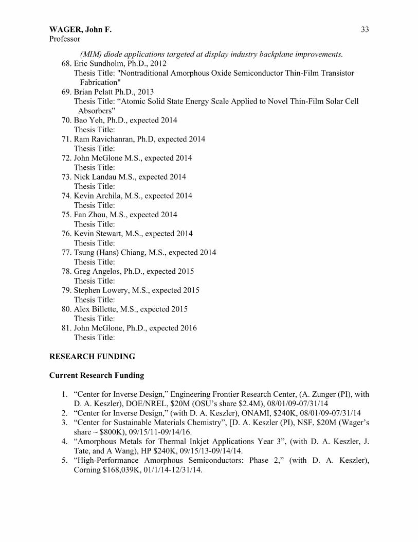
WAGER, John F. Professor
33
(MIM) diode applications targeted at display industry backplane improvements. 68. Eric Sundholm, Ph.D., 2012 Thesis Title: "Nontraditional Amorphous Oxide Semiconductor Thin-Film Transistor Fabrication" 69. Brian Pelatt Ph.D., 2013 Thesis Title: “Atomic Solid State Energy Scale Applied to Novel Thin-Film Solar Cell Absorbers” 70. Bao Yeh, Ph.D., expected 2014 Thesis Title: 71. Ram Ravichanran, Ph.D, expected 2014 Thesis Title: 72. John McGlone M.S., expected 2014 Thesis Title: 73. Nick Landau M.S., expected 2014 Thesis Title: 74. Kevin Archila, M.S., expected 2014 Thesis Title: 75. Fan Zhou, M.S., expected 2014 Thesis Title: 76. Kevin Stewart, M.S., expected 2014 Thesis Title: 77. Tsung (Hans) Chiang, M.S., expected 2014 Thesis Title: 78. Greg Angelos, Ph.D., expected 2015 Thesis Title: 79. Stephen Lowery, M.S., expected 2015 Thesis Title: 80. Alex Billette, M.S., expected 2015 Thesis Title: 81. John McGlone, Ph.D., expected 2016 Thesis Title: RESEARCH FUNDING Current Research Funding
1. “Center for Inverse Design,” Engineering Frontier Research Center, (A. Zunger (PI), with D. A. Keszler), DOE/NREL, $20M (OSU’s share $2.4M), 08/01/09-07/31/14
2. “Center for Inverse Design,” (with D. A. Keszler), ONAMI, $240K, 08/01/09-07/31/14 3. “Center for Sustainable Materials Chemistry”, [D. A. Keszler (PI), NSF, $20M (Wager’s
share ~ $800K), 09/15/11-09/14/16. 4. “Amorphous Metals for Thermal Inkjet Applications Year 3”, (with D. A. Keszler, J.
Tate, and A Wang), HP $240K, 09/15/13-09/14/14. 5. “High-Performance Amorphous Semiconductors: Phase 2,” (with D. A. Keszler),
Corning $168,039K, 01/1/14-12/31/14.

WAGER, John F. Professor
34
6. “Amorphous Semiconductor Electronics for SOC Backend Logic / Memory,” SRC/Intel $225,000, 04/1/12-03/31/15.
Prior Research Funding
1. "Defects in Semiconductors," (with J. A. Van Vechten), Air Force Office of Scientific Research, $150,000, October 1986-April 1989.
2. "Diamond-Like Carbon Electroluminescent Display," Battelle/Army Research Office, $21,000, July 1987-December 1987.
3. "Identification of the Instability Mechanism of ZnS:Mn Electroluminescent Devices," Planar Systems, Inc., $19,201, June 15, 1989-September 15, 1989.
4. "Optically Controlled Dislocation Climb and Glide to Remove DX and Other Defects from Device Regions of Strained-Layers," (with J. A. Van Vechten, T. K. Plant, and J. R. Arthur), $85,701, January 15, 1989-June 30, 1990.
5. "GaN Electroluminescence," Battelle/Army Research Office, $30,210, November 22, 1989-November 22, 1990.
6. "Atomic Approaches to Defect Thermochemistry," (with J. A. Van Vechten), Air Force Office of Scientific Research, $316,409, April 1989-April 1992.
7. "Bandgap Engineering Dielectrics for Electroluminescence Applications," Goldstar Com-pany, Ltd., $72,770, June 1991-June 1993.
8. "Hot Electron Physics of Alternating-Current Thin-Film Electroluminescent Devices," (with S.M. Goodnick), Army Research Office, $325,000, July 1991-May 1994.
9. "Phosphor Technology Center of Excellence," (with S. M. Goodnick and T. K. Plant), Defense Advanced Research Projects Agency, $300,000, Aug. 1993-Aug. 1994; $294,000, Aug. 1994-Aug. 1995; $224,346, Aug. 1995-Aug. 1996; $144,477; Aug. 1996-Aug. 1997; $110,858, Aug. 1997-Aug. 1998; $117,000, Aug. 1998-Aug. 1999; $109,348, Aug. 1999- March 2001; TOTAL = $1,085,627
10. "Synthesis of Flat-Panel Phosphors," (with V. D. Bondar, Lviv State University, Ukraine), NATO Travel Grant, $5,592, Summer 1995-Fall 1996.
11. "Trivalent Phosphors for ACTFEL Applications," ARO, $89,265, June 1994-June 1997. 12. "Hot Electron Physics of Alternating-Current Thin-Film Electroluminescent Devices:
Phase II," ARO, (with S. M. Goodnick and T. K. Plant), $250,000, Aug. 1994-Sept. 1997.
13. "Next Generation High Resolution and Color Display Consortium," Planar/DARPA, (with D. Allstot and V. K. Tripathi), $200,000, April 1995-September 1997.
14. "Synthesis of Flat-Panel Phosphors: Phase II," (with V. D. Bondar, Lviv State University, Ukraine), NATO Travel Grant, $5,970, Summer 1997-Summer 1999.
15. "Next Generation EL Display Consortium," Planar/DARPA, (with T. K. Plant), $200,000, October 1997-September 1999.
16. "Organic Electroluminescent Device Characterization and Modeling," ARO, $82,803, June 1997-May 2000.
17. "Organic Light-Emitting Device (OLED) Fabrication," (with M. D. Koretsky and D. A. Keszler), OSU/College of Engineering, $50,000, June 1999-June 2000.
18. "Phosphor Development for Electroluminescent Displays," (with A.W. Sleight and T.K. Plant), NSF / GOALI, $484,378, August 1997-August 2000.
19. “Fast-Track Materials Development and Study of Wide Band-Gap Semiconductors,” (with D. A. Keszler) HP, $75,678, January 2002-July 2002.
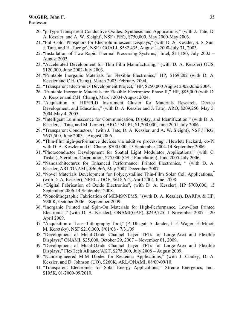
WAGER, John F. Professor
35
20. "p-Type Transparent Conductive Oxides: Synthesis and Applications," (with J. Tate, D. A. Keszler, and A. W. Sleight), NSF / FRG, $750,000, May 2000-May 2003.
21. "Full-Color Phosphors for Electroluminescent Displays," (with D. A. Keszler, S. S. Sun, J. Tate, and R. Tuenge), NSF / GOALI, $582,435, August 1, 2000-July 31, 2003.
22. “Installation of Two Rapid Thermal Processing Systems,” Intel, $11,180, July 2002 – August 2003.
23. “Accelerated Development for Thin Film Manufacturing,” (with D. A. Keszler) OUS, $120,000, June 2002-July 2003.
24. “Printable Inorganic Materials for Flexible Electronics,” HP, $169,202 (with D. A. Keszler and C.H. Chang), March 2003-February 2004.
25. “Transparent Electronics Development Project,” HP, $250,000 August 2002-June 2004. 26. “Printable Inorganic Materials for Flexible Electronics: Phase II,” HP, $85,000 (with D.
A. Keszler and C.H. Chang), March 2004-August 2004. 27. “Acquisition of HIP/PLD Instrument Cluster for Materials Research, Device
Development, and Education,” (with D. A. Keszler and J. Tate), ARO, $209,250, May 5, 2004-May 4, 2005.
28. “Intelligent Luminescence for Communication, Display, and Identification,” (with D. A. Keszler, J. Tate, and M. Lerner), ARO / MURI, $1,200,000, June 2001-July 2006.
29. “Transparent Conductors," (with J. Tate, D. A. Keszler, and A. W. Sleight), NSF / FRG, $637,500, June 2003 – August 2006.
30. “Thin-film high-performance devices via additive processing”, Hewlett Packard, co-PI with D. A. Keszler and C. Chang, $700,000, 15 September 2004-14 September 2006.
31. “Photoconductor Development for Spatial Light Modulator Applications,” (with C. Tasker), Steridian, Corporation, $75,000 (OSU Foundation), June 2005-July 2006.
32. “Nanoarchitectures for Enhanced Performance: Printed Electronics, “ (with D. A. Keszler, ARL/ONAMI, $96,966, May 2007-December 2007.
33. “Novel Materials Development for Polycrystalline Thin-Film Solar Cell Applications,”
(with D. A. Keszler), NREL / DOE, $618,612, April 2004-June. 2008. 34. “Digital Fabrication of Oxide Electronics”, (with D. A. Keszler), HP $700,000, 15
September 2006-14 September 2008. 35. “Nonolithographic Fabrication of MEMS/NEMS,” (with D. A. Keszler), DARPA & HP,
$900K, October 2006 – September 2009. 36. “Inorganic Printed and Spin-On Materials for High-Performance, Low-Cost Printed
Electronics,” (with D. A. Keszler), ONAMI(GAP), $249,725, 1 November 2007 – 20 April 2009.
37. “Acquisition of Laser Lithography Tool,” (P. Dhagat, A. Jander, J. F. Wager, E. Minot, M. Koretsky), NSF $210,000, 8/01/08 - 7/31/09
38. “Development of Metal-Oxide Channel Layer TFTs for Large-Area and Flexible Displays,” ONAMI, $25,000, October 29, 2007 – November 01, 2009.
39. “Development of Metal-Oxide Channel Layer TFTs for Large-Area and Flexible Displays,” FlexTech Alliance/AKT, $275,000, July 2008 – August 2009.
40. “Nanoengineered MIM Diodes for Rectenna Applications,” (with J. Conley, D. A. Keszler, and D. Johnson (UO), $260K, ARL/ONAMI, 08/09-09/10.
41. “Transparent Electronics for Solar Energy Applications,” Xtreme Energetics, Inc., $105K, 01/2009-09/2010.
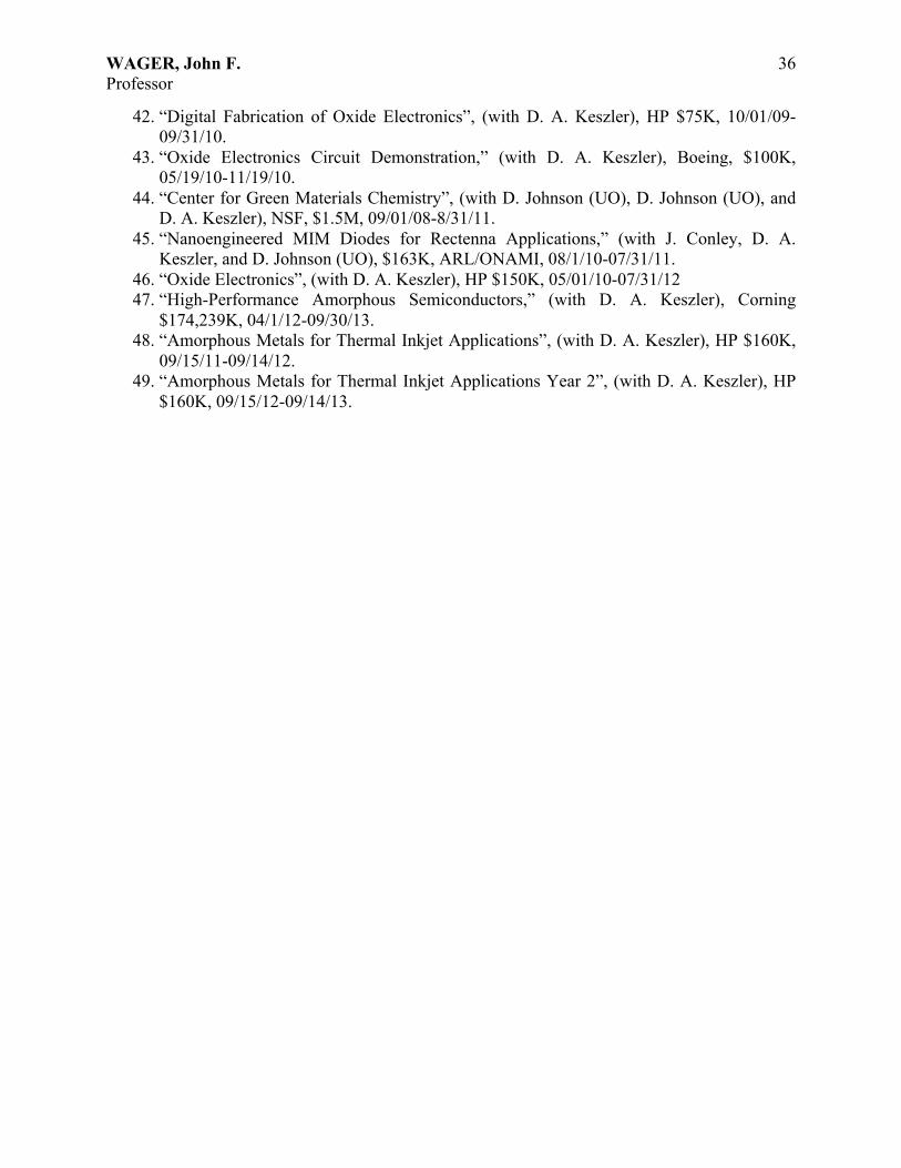
WAGER, John F. Professor
36
42. “Digital Fabrication of Oxide Electronics”, (with D. A. Keszler), HP $75K, 10/01/09-09/31/10.
43. “Oxide Electronics Circuit Demonstration,” (with D. A. Keszler), Boeing, $100K, 05/19/10-11/19/10.
44. “Center for Green Materials Chemistry”, (with D. Johnson (UO), D. Johnson (UO), and D. A. Keszler), NSF, $1.5M, 09/01/08-8/31/11.
45. “Nanoengineered MIM Diodes for Rectenna Applications,” (with J. Conley, D. A. Keszler, and D. Johnson (UO), $163K, ARL/ONAMI, 08/1/10-07/31/11.
46. “Oxide Electronics”, (with D. A. Keszler), HP $150K, 05/01/10-07/31/12 47. “High-Performance Amorphous Semiconductors,” (with D. A. Keszler), Corning
$174,239K, 04/1/12-09/30/13. 48. “Amorphous Metals for Thermal Inkjet Applications”, (with D. A. Keszler), HP $160K,
09/15/11-09/14/12. 49. “Amorphous Metals for Thermal Inkjet Applications Year 2”, (with D. A. Keszler), HP
$160K, 09/15/12-09/14/13.


![JFW テキスタイル・フェア 2017AW【開催報告】...2016/12/26 · 8.Dec 2016 JFW Tex.Div 1 JFW テキスタイル・フェア 2017AW【開催報告】 [ 会期 ] 2016年11月29日(火)~30日(水)](https://cdn.vdocuments.net/doc/165x107/5ff2def4fb9aa202506154c9/jfw-ffff-2017awe-20161226-8dec.jpg)


