WARREN M. ROHSENOW HEAT AND MASS TRANSFER LABORATORYNanoEngineering GroupNanoEngineering Group
ENERGY NANOTECHNOLOGY--- A Few Examples
Gang Chen
Nanoengineering GroupRohsenow Heat and Mass Transfer Laboratory
Massachusetts Institute of Technology
Cambridge, MA 02139
Email: [email protected]://web.mit.edu/nanoengineering
WARREN M. ROHSENOW HEAT AND MASS TRANSFER LABORATORYNanoEngineering GroupNanoEngineering Group
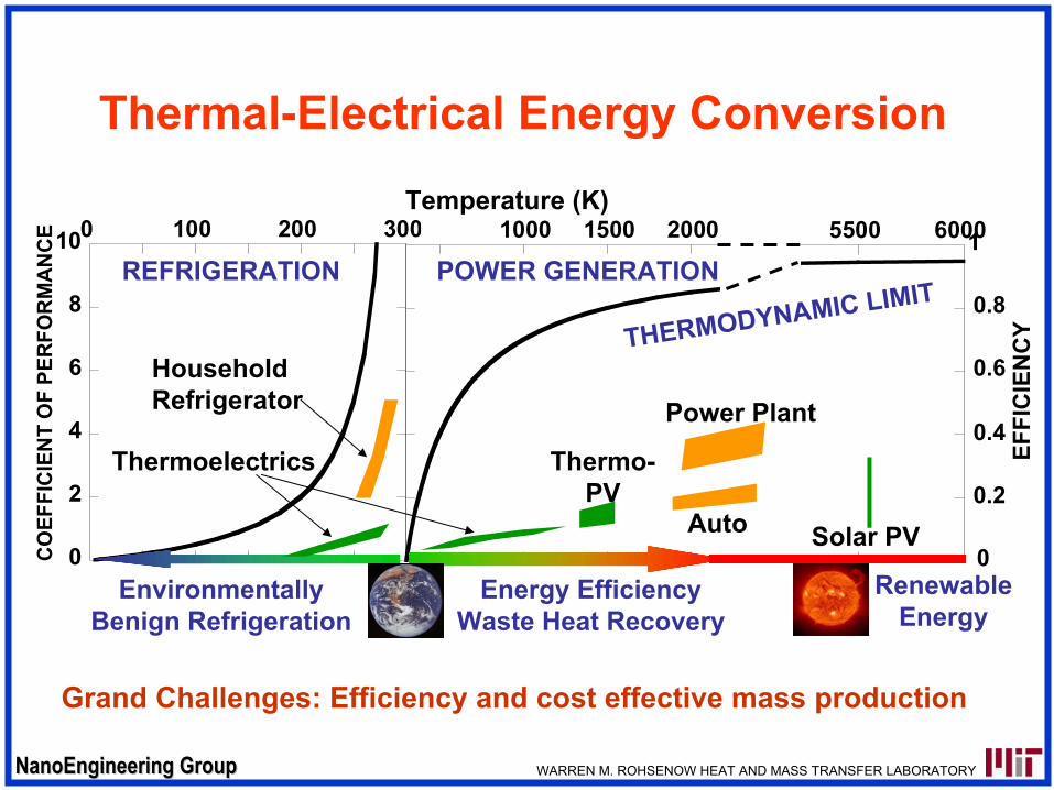
Thermal-Electrical Energy ConversionTemperature (K)
Grand Challenges: Efficiency and cost effective mass production
500 1000 1500 2000 25005000 5500 6000
EFFI
CIE
NC
Y
0
0.2
0.4
0.6
0.8
1
0
2
4
6
8
100 50 100 150 200 250 300
CO
EFFI
CIE
NT
OF
PER
FOR
MA
NC
E
REFRIGERATION POWER GENERATION
THERMODYNAMIC LIMIT
Power Plant
Auto Solar PV
Thermo-PV
Thermoelectrics
HouseholdRefrigerator
EnvironmentallyBenign Refrigeration
Energy EfficiencyWaste Heat Recovery
RenewableEnergy
WARREN M. ROHSENOW HEAT AND MASS TRANSFER LABORATORYNanoEngineering GroupNanoEngineering Group
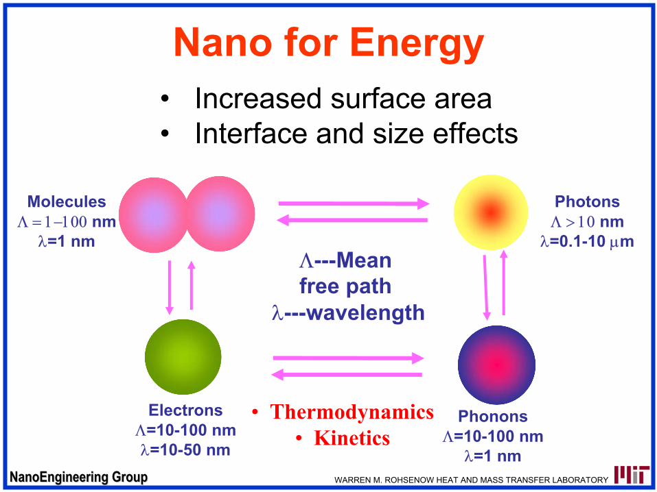
Nano for Energy• Increased surface area• Interface and size effects
PhotonsΛ > 10 nm
λ=0.1-10 µm
PhononsΛ=10-100 nm
λ=1 nm
ElectronsΛ=10-100 nmλ=10-50 nm
Λ---Mean free path
λ---wavelength
MoleculesΛ = 1−100 nm
λ=1 nm
• Thermodynamics• Kinetics
WARREN M. ROHSENOW HEAT AND MASS TRANSFER LABORATORYNanoEngineering GroupNanoEngineering Group
Phonon and Electron Engineering for
Thermoelectric Materials
WARREN M. ROHSENOW HEAT AND MASS TRANSFER LABORATORYNanoEngineering GroupNanoEngineering Group
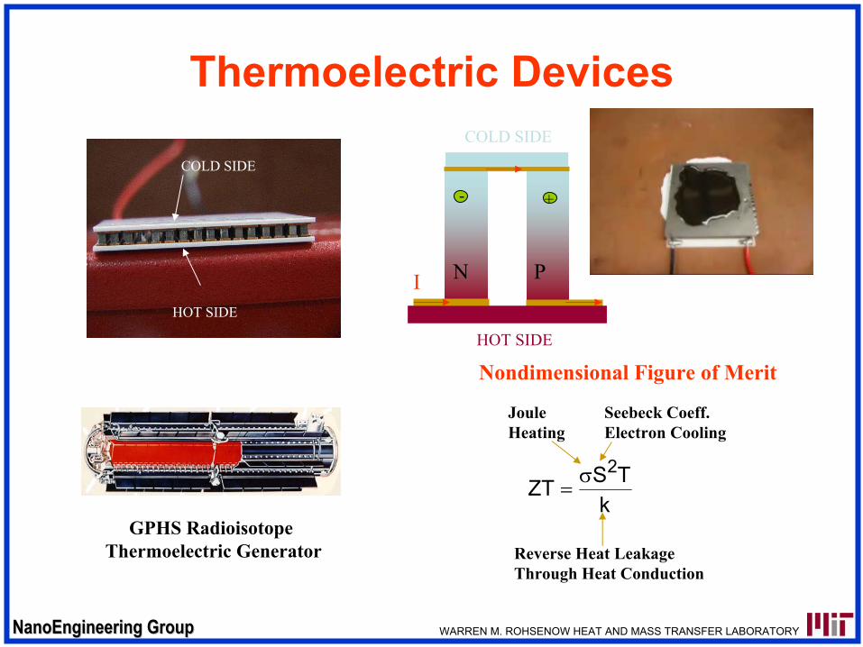
Thermoelectric Devices
COLD SIDE
HOT SIDE
-
I
+
N P
HOT SIDE
COLD SIDE
Nondimensional Figure of Merit
kTSZT
2σ=
Reverse Heat Leakage Through Heat Conduction
Joule Heating
Seebeck Coeff.Electron Cooling
GPHS Radioisotope Thermoelectric Generator
WARREN M. ROHSENOW HEAT AND MASS TRANSFER LABORATORYNanoEngineering GroupNanoEngineering Group
0
0.5
1
1.5
2
2.5
3
3.5
4
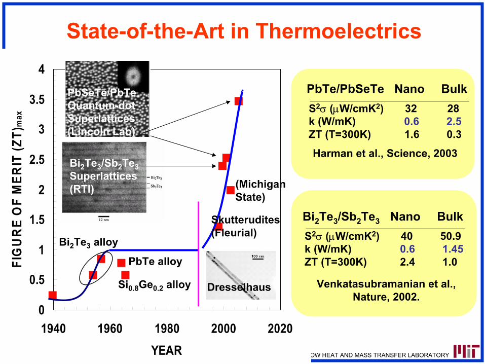
1940 1960 1980 2000 2020YEAR
FIG
UR
E O
F M
ERIT
(ZT)
max
Bi2Te3 alloy
PbTe alloy
Si0.8Ge0.2 alloy
PbTe/PbSeTeS2σ (µW/cmK2) 32 28k (W/mK) 0.6 2.5 ZT (T=300K) 1.6 0.3
BulkNano
Harman et al., Science, 2003
Bi2Te3/Sb2Te3
S2σ (µW/cmK2) 40 50.9k (W/mK) 0.6 1.45 ZT (T=300K) 2.4 1.0
BulkNano
Venkatasubramanian et al., Nature, 2002.
Skutterudites(Fleurial)
PbSeTe/PbTeQuantum-dotSuperlattices(Lincoln Lab)
Bi2Te3/Sb2Te3Superlattices(RTI)
Dresselhaus
State-of-the-Art in Thermoelectrics
(MichiganState)
WARREN M. ROHSENOW HEAT AND MASS TRANSFER LABORATORYNanoEngineering GroupNanoEngineering Group
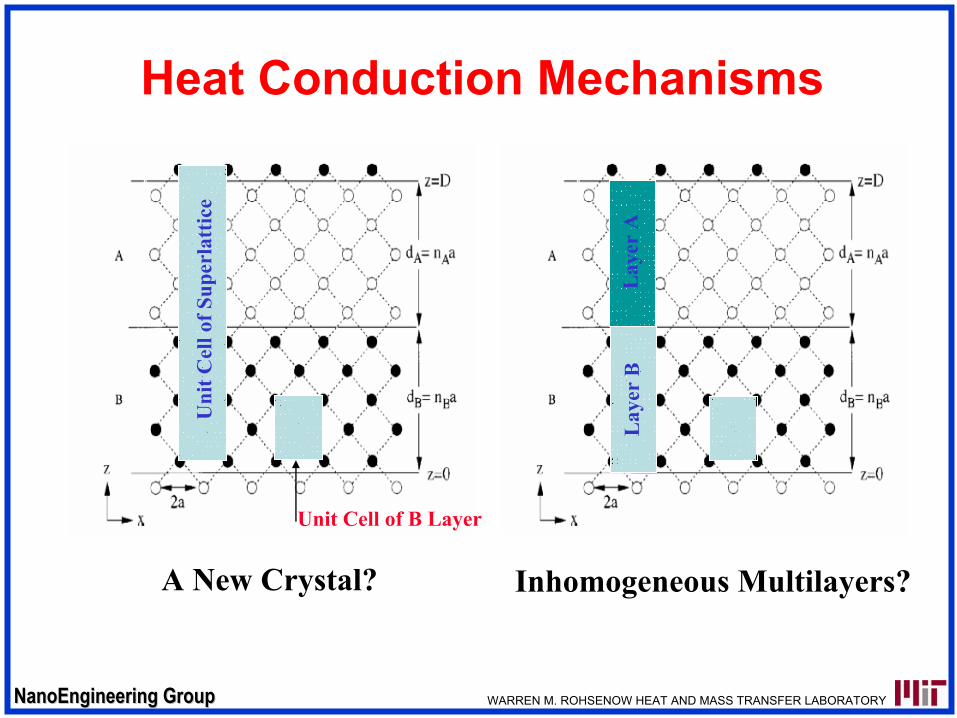
Heat Conduction Mechanisms
A New Crystal? Inhomogeneous Multilayers?
Uni
t Cel
l of S
uper
latt
ice
Unit Cell of B Layer
Lay
er B
Lay
er A
WARREN M. ROHSENOW HEAT AND MASS TRANSFER LABORATORYNanoEngineering GroupNanoEngineering Group
0
20
40
60
80
10 1 10 2 10 3 10 4
THER
MA
L C
ON
DU
CTI
VITY
(W/m
K)
LAYER THICKNESS (Å)
BULK
SPECULAR (p=1)
p=0.95
p=0.8DIFFUSE (p=0)
Yao (1987)Yu et al. (1995)0
20
40
60
80
10 1 10 2 10 3 10 40
20
40
60
80
0
20
40
60
80
10 1 10 2 10 3 10 410 1 10 2 10 3 10 4
THER
MA
L C
ON
DU
CTI
VITY
(W/m
K)
LAYER THICKNESS (Å)
BULK
SPECULAR (p=1)
p=0.95
p=0.8DIFFUSE (p=0)
Yao (1987)Yu et al. (1995)
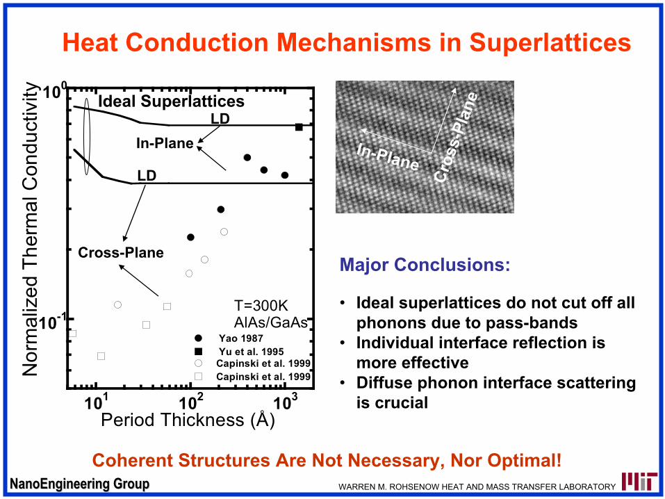
Heat Conduction Mechanisms in Superlattices
Coherent Structures Are Not Necessary, Nor Optimal!
Major Conclusions:
• Ideal superlattices do not cut off all phonons due to pass-bands
• Individual interface reflection is more effective
• Diffuse phonon interface scattering is crucial
10-1
100
101 102 103
Capinski et al. 1999Capinski et al. 1999
Yao 1987 Yu et al. 1995
Nor
mal
ized
The
rmal
Con
duct
ivity
Period Thickness (Å)
T=300KAlAs/GaAs
In-Plane
Cross-Plane
LD
LD
Ideal Superlattices
In-Plane
Cros
s-Pl
ane
WARREN M. ROHSENOW HEAT AND MASS TRANSFER LABORATORYNanoEngineering GroupNanoEngineering Group
Photon Engineering:Thermophovoltaics
WARREN M. ROHSENOW HEAT AND MASS TRANSFER LABORATORYNanoEngineering GroupNanoEngineering Group
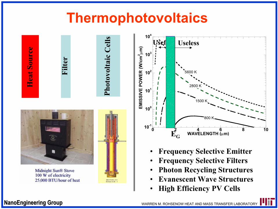
ThermophotovoltaicsH
eat S
ourc
e
Phot
ovol
taic
Ce l
ls
Filte
r
• Frequency Selective Emitter• Frequency Selective Filters• Photon Recycling Structures• Evanescent Wave Structures• High Efficiency PV Cells
10-1
100
101
102
103
104
0 2 4 6 8 10
EMIS
SIVE
PO
WER
(W/c
m2 µm
)WAVELENGTH (µm)
5600 K
2800 K
1500 K
800 K
EG
UselessUseful
WARREN M. ROHSENOW HEAT AND MASS TRANSFER LABORATORYNanoEngineering GroupNanoEngineering Group
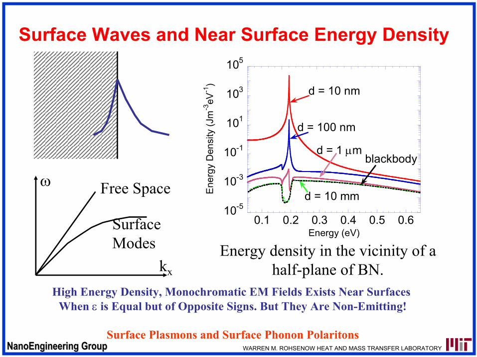
ω Free Space
kx
SurfaceModes Energy density in the vicinity of a
half-plane of BN.High Energy Density, Monochromatic EM Fields Exists Near Surfaces
When ε is Equal but of Opposite Signs. But They Are Non-Emitting!
Surface Plasmons and Surface Phonon Polaritons
10-5
10-3
10-1
101
103
105
0.1 0.2 0.3 0.4 0.5 0.6
5 10 15 20 25
Energy (eV)
Ene
rgy
Den
sity
(Jm
-3eV
-1)
Wavelength (µm)
d = 10 nm
d = 100 nm
d = 1 µm
d = 10 mm
blackbody
Surface Waves and Near Surface Energy Density
WARREN M. ROHSENOW HEAT AND MASS TRANSFER LABORATORYNanoEngineering GroupNanoEngineering Group
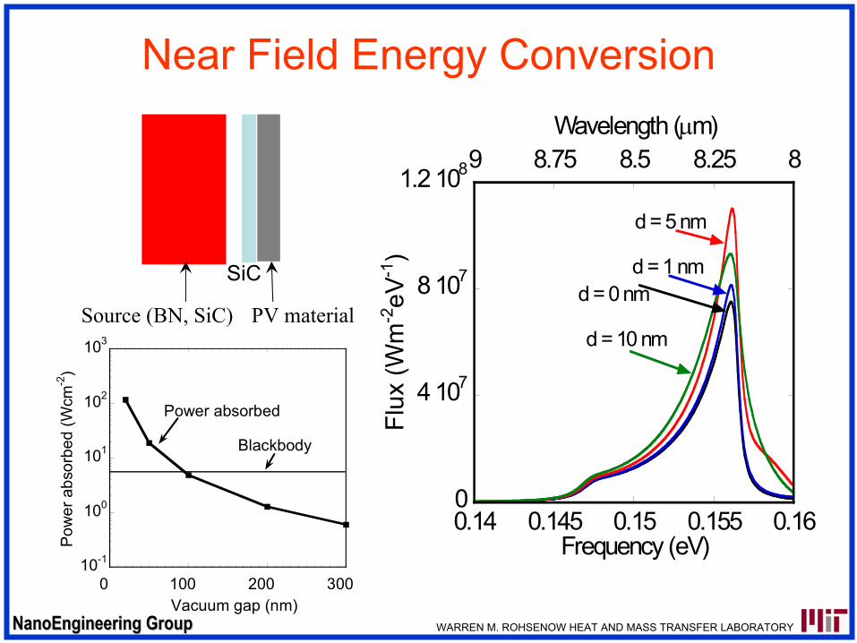
Near Field Energy Conversion
10-1
100
101
102
103
0 100 200 300
Pow
er a
bsor
bed
(Wcm
-2)
Vacuum gap (nm)
Power absorbed
Blackbody
0
4 107
8 107
1.2 108
0.14 0.145 0.15 0.155 0.16
88.258.58.759
Flux
(Wm
-2eV
-1)
Frequency (eV)
Wavelength (µm)
d = 0 nmd = 1 nm
d = 5 nm
d = 10 nmSource (BN, SiC) PV material
SiC
WARREN M. ROHSENOW HEAT AND MASS TRANSFER LABORATORYNanoEngineering GroupNanoEngineering Group
Coupled Conduction and RadiationNonequilibrium Thermoelectric Devices
WARREN M. ROHSENOW HEAT AND MASS TRANSFER LABORATORYNanoEngineering GroupNanoEngineering Group
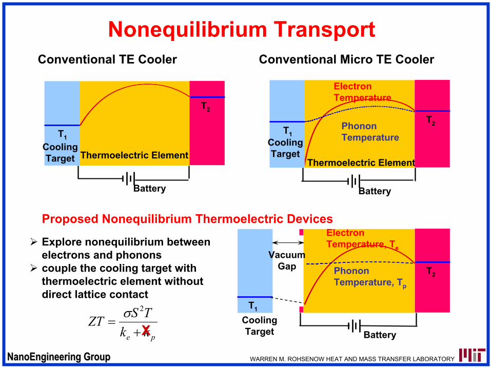
Nonequilibrium Transport
Battery
Proposed Nonequilibrium Thermoelectric Devices
Explore nonequilibrium between electrons and phonons couple the cooling target with thermoelectric element without direct lattice contact
pe kkTSZT
+=
2σX
CoolingTarget
T1
Electron Temperature, Te
Phonon Temperature, Tp
VacuumGap
Battery
T2
Conventional Micro TE Cooler
T1
Electron Temperature
Phonon TemperatureCooling
TargetThermoelectric Element
T2
Conventional TE Cooler
T1Cooling Target Thermoelectric Element
Battery
T2
WARREN M. ROHSENOW HEAT AND MASS TRANSFER LABORATORYNanoEngineering GroupNanoEngineering Group
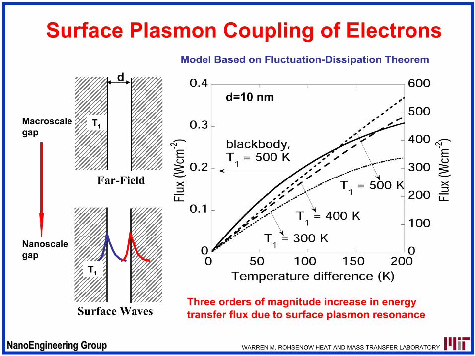
Surface Waves
Far-Field
d
Three orders of magnitude increase in energy transfer flux due to surface plasmon resonance
Nanoscalegap
Macroscale gap
d=10 nm
Model Based on Fluctuation-Dissipation Theorem
Surface Plasmon Coupling of Electrons
T1
T1
WARREN M. ROHSENOW HEAT AND MASS TRANSFER LABORATORYNanoEngineering GroupNanoEngineering Group
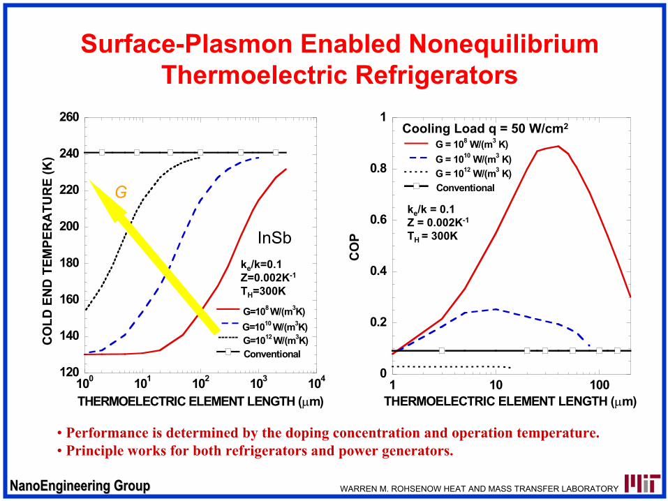
ke/k=0.1Z=0.002K-1
TH=300K
120
140
160
180
200
220
240
260
100 101 102 103 104
THERMOELECTRIC ELEMENT LENGTH (µm)
CO
LD E
ND
TEM
PER
ATU
RE
(K)
G=108 W/(m3K)G=1010 W/(m3K)G=1012 W/(m3K)Conventional
Surface-Plasmon Enabled NonequilibriumThermoelectric Refrigerators
• Performance is determined by the doping concentration and operation temperature.• Principle works for both refrigerators and power generators.
0
0.2
0.4
0.6
0.8
1
1 10 100THERMOELECTRIC ELEMENT LENGTH (µm)
CO
P
G = 108 W/(m3 K)G = 1010 W/(m3 K)G = 1012 W/(m3 K)Conventional
ke/k = 0.1Z = 0.002K-1
TH = 300K
Cooling Load q = 50 W/cm2
InSb
G
WARREN M. ROHSENOW HEAT AND MASS TRANSFER LABORATORYNanoEngineering GroupNanoEngineering Group
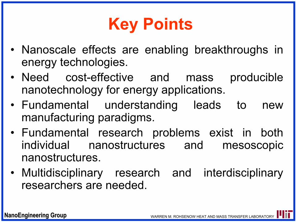
Key Points• Nanoscale effects are enabling breakthroughs in
energy technologies.• Need cost-effective and mass producible
nanotechnology for energy applications.• Fundamental understanding leads to new
manufacturing paradigms. • Fundamental research problems exist in both
individual nanostructures and mesoscopicnanostructures.
• Multidisciplinary research and interdisciplinary researchers are needed.
WARREN M. ROHSENOW HEAT AND MASS TRANSFER LABORATORYNanoEngineering GroupNanoEngineering Group
ACKNOWLEDGMENTS• Current Members
H. Asegun (Molecular Dynamics)V. Berube (hydrogen storage)Z. Chen (Metamaterials, TPV)S. Goh (polymers)T. Harris (Thermoelectrics&Nanomaterials)Q. Hao (Thermoelectrics)D. Kramer (Solar thermoelectrics)H. Lee (Thermoelectric Materials)H. Lu (TPV and PV)A. Minnich (thermoelectrics)A. Muto (nanowires and thermoelectrics)S. Nakamura (nanowires and thermoelectrics)A. Narayanaswamy (Metamaterials, TPV)G. Radtke (hydrogen storage)A. Schmidt (ps pump-and-probe)E. Skow (polymers)S. Shen (lubrication, rarefied gas dynamics)Dr. M. Chieso (nanofluids)Dr. X. Chen (thermoelectrics, Pump-and-Probe)Dr. D. Vashee (thermoelectrics)Prof. Y.T. Kang (nanofluids)
• CollaboratorsM.S. & G. Dresselhaus (MIT, NW&CNT, Theory)J.-P. Fleurial (JPL, Thermoelectric Devices) J. Joannopoulos (MIT, Photonic Crystals)Z.F. Ren (BC, Thermoelectric Materials, CNT)X. Zhang (Berkeley, Metamaterials)
• Past Members (Partial List)Prof. C. Dames (Nanowires, UC Riverside)Prof. D. Borca-Tasciuc (Nanowires, RPI)Prof. T. Borca-Tasciuc (Thermoelectrics,RPI)Dr. F. Hashemi (Nano-Device Fabrication)Dr. A. Jacquot (TE Device Fabrication)Dr. M.S. Jeng (Nanocomposites, ITRI)Dr. R. Kumar (Thermoelectric Device Modeling)Dr. W.L. Liu (superlattice)Dr. D. Song (TE and Monte Carlo, Intel)Dr. S.G. Volz (MD, Ecole Centrale de Paris)Prof. B. Yang (TE and Phonons, U. Maryland)Prof. R.G. Yang (Nanocomposites, U. Colorado)Prof. D.-J. Yao (TE Devices, Tsinghua Univ.)Prof. T. Zeng (Thermionics, NCSU)
Sponsors: ARO, DOE, NASA, NSF, ONR, Industries


