Download - ESE 568: Mixed Signal Design and Modeling

ESE 568: Mixed Signal Design and Modeling
Lec 10: October 2, 2019 Sampling Circuits
Penn ESE 568 Fall 2019 - Khanna adapted from Murmann EE315B, Stanford

Outline
! Elementary track-and-hold circuit and its nonidealities
! First order improvements to elementary track-and-hold
2 Penn ESE 568 Fall 2019 - Khanna adapted from Murmann EE315B, Stanford
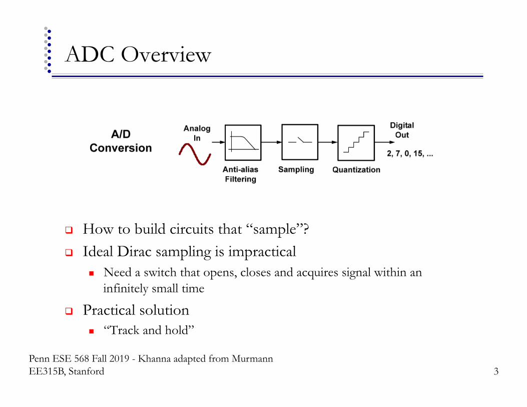
ADC Overview
! How to build circuits that “sample”? ! Ideal Dirac sampling is impractical
" Need a switch that opens, closes and acquires signal within an infinitely small time
! Practical solution " “Track and hold”
3 Penn ESE 568 Fall 2019 - Khanna adapted from Murmann EE315B, Stanford

Ideal Track-and-Hold Circuit
4 Penn ESE 568 Fall 2019 - Khanna adapted from Murmann EE315B, Stanford

Signal Nomenclature
5 Penn ESE 568 Fall 2019 - Khanna adapted from Murmann EE315B, Stanford
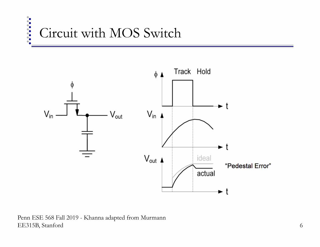
Circuit with MOS Switch
6 Penn ESE 568 Fall 2019 - Khanna adapted from Murmann EE315B, Stanford
Nonidealities
! kTC noise ! Finite acquisition time ! Tracking nonlinearity ! Signal dependent hold instant ! Charge injection and clock feedthrough ! Thermal noise ! Clock jitter ! Hold mode feedthrough and leakage
7 Penn ESE 568 Fall 2019 - Khanna adapted from Murmann EE315B, Stanford

kTC Noise
! Equivalent circuit in track mode
8 Penn ESE 568 Fall 2019 - Khanna adapted from Murmann EE315B, Stanford

kTC Noise
! Equivalent circuit in track mode
9 Penn ESE 568 Fall 2019 - Khanna adapted from Murmann EE315B, Stanford

kTC Noise
! If we make kT/C noise equal to quantization noise
10 Penn ESE 568 Fall 2019 - Khanna adapted from Murmann EE315B, Stanford

kTC Noise
! If we make kT/C noise equal to quantization noise
11 Penn ESE 568 Fall 2019 - Khanna adapted from Murmann EE315B, Stanford

Finite Acquisition Time
! Consider various input signal scenarios
! 1. Input is a sampled data signal, i.e. the output of another switched capacitor stage
! 2. Input is a slowly varying continuous time signal, e.g. the input of an oversampling ADC
! 3. Input is a rapidly varying continuous time signal, e.g. the input of a Nyquist or subsampling DAC
12 Penn ESE 568 Fall 2019 - Khanna adapted from Murmann EE315B, Stanford

Finite Acquisition Time – Case 1
! For simplicity, neglect finite rise time of the input signal ! Consider worst case – the output is required to settle from 0
to the full-scale voltage of the system (VFS) within Ts/2
13 Penn ESE 568 Fall 2019 - Khanna adapted from Murmann EE315B, Stanford

Finite Acquisition Time – Case 1
! For simplicity, neglect finite rise time of the input signal ! Consider worst case – the output is required to settle from 0
to the full-scale voltage of the system (VFS) within Ts/2
14 Penn ESE 568 Fall 2019 - Khanna adapted from Murmann EE315B, Stanford

Finite Acquisition Time – Case 1
! For simplicity, neglect finite rise time of the input signal ! Consider worst case – the output is required to settle from 0
to the full-scale voltage of the system (VFS) within Ts/2
15 Penn ESE 568 Fall 2019 - Khanna adapted from Murmann EE315B, Stanford

Finite Acquisition Time – Case 1
16 Penn ESE 568 Fall 2019 - Khanna adapted from Murmann EE315B, Stanford

Finite Acquisition Time – Case 1
! Typically think about settling error in terms of the number of settling time constants (N) required for ½ LSB settling in a B-bit system
17 Penn ESE 568 Fall 2019 - Khanna adapted from Murmann EE315B, Stanford

Finite Acquisition Time – Case 1
! Typically think about settling error in terms of the number of settling time constants (N) required for ½ LSB settling in a B-bit system
18 Penn ESE 568 Fall 2019 - Khanna adapted from Murmann EE315B, Stanford

Finite Acquisition Time – Case 2 & 3
! Consider a sinusoidal input around “0”, and “0” also as the initial condition for Vout (for notational simplicity)
19 Penn ESE 568 Fall 2019 - Khanna adapted from Murmann EE315B, Stanford

Finite Acquisition Time – Case 2 & 3
! Consider a sinusoidal input around “0”, and “0” also as the initial condition for Vout (for notational simplicity)
20 Penn ESE 568 Fall 2019 - Khanna adapted from Murmann EE315B, Stanford

Finite Acquisition Time – Case 2 & 3
! At t=TS/2, the error in the held signal consists of two parts ! Residual error due to initial exponential decaying initial
transient term " In order to minimize this error, we need to choose N appropriately,
as calculated for the step input scenario
! Error due to magnitude attenuation and phase shift in the
steady state term " This error depends only on the RC time constant and the input
frequency; it cannot be reduced by extending the length of the track phase
" How significant is the error due to the steady-state term?
21 Penn ESE 568 Fall 2019 - Khanna adapted from Murmann EE315B, Stanford

Finite Acquisition Time – Case 2 & 3
! As an example, let’s compute the percent amplitude error for the N values derived previously (½ LSB B-bit settling to a step)
22 Penn ESE 568 Fall 2019 - Khanna adapted from Murmann EE315B, Stanford

Finite Acquisition Time – Case 2 & 3
! As an example, let’s compute the percent amplitude error for the N values derived previously (½ LSB B-bit settling to a step)
23 Penn ESE 568 Fall 2019 - Khanna adapted from Murmann EE315B, Stanford

Finite Acquisition Time – Case 2 & 3
! As an example, let’s compute the percent amplitude error for the N values derived previously (½ LSB B-bit settling to a step)
24 Penn ESE 568 Fall 2019 - Khanna adapted from Murmann EE315B, Stanford

Finite Acquisition Time – Case 2 & 3
! As an example, let’s compute the percent amplitude error for the N values derived previously (½ LSB B-bit settling to a step)
25 Penn ESE 568 Fall 2019 - Khanna adapted from Murmann EE315B, Stanford

Summary – Finite Acquisition Time
! Precise settling to an input step is accomplished within 5-13 RC time constants (depending on precision)
! Precise tracking of a high-frequency continuous time input signal tends to impose more stringent requirements " Number to remember: ~1% attenuation error at Nyquist (fin=fS/2)
for N ~ 10 (B=14)
26 Penn ESE 568 Fall 2019 - Khanna adapted from Murmann EE315B, Stanford

Summary – Finite Acquisition Time
! Precise settling to an input step is accomplished within 5-13 RC time constants (depending on precision)
! Precise tracking of a high-frequency continuous time input signal tends to impose more stringent requirements " Number to remember: ~1% attenuation error at Nyquist (fin=fS/2)
for N ~ 10 (B=14)
! In applications where attenuation is tolerable, the RC time constant constant requirements then tend to follow from the distortion specs " The larger the attenuation, the larger the instantaneous voltage drop
across the (weakly nonlinear) MOSFET # undesired harmonics " Let’s look at that next…
27 Penn ESE 568 Fall 2019 - Khanna adapted from Murmann EE315B, Stanford
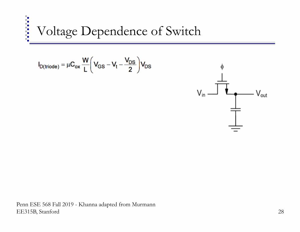
Voltage Dependence of Switch
28 Penn ESE 568 Fall 2019 - Khanna adapted from Murmann EE315B, Stanford

Voltage Dependence of Switch
! Two problems " RON is modulated by Vin (assuming Φ=VDD=constant) " Transistor turn off is signal dependent, occurs when Vin= Φ-VT
29 Penn ESE 568 Fall 2019 - Khanna adapted from Murmann EE315B, Stanford

Track Mode Nonlinearity
! Output tracks well when input voltage is low " Gets distorted when input voltage is high due to increase
in RON
30 Penn ESE 568 Fall 2019 - Khanna adapted from Murmann EE315B, Stanford

Analysis
! “All” we need to do is solve the above differential equation. NBD.
! Luckily someone has already done it for us " See [Yu, TCAS II, 2/1999]
31 Penn ESE 568 Fall 2019 - Khanna adapted from Murmann EE315B, Stanford

Result
! For low distortion " Make amplitude smaller than VGS-VT
" Low swing # bad for SNR
" Make 1/τ much larger than ω (input frequency) " Big switch # may cost lots of power to drive, comes with large parasitic
capacitances
32 Penn ESE 568 Fall 2019 - Khanna adapted from Murmann EE315B, Stanford

Numerical Example
33 Penn ESE 568 Fall 2019 - Khanna adapted from Murmann EE315B, Stanford
! Parameters:
! Not great…

SFDR
! Definition of "Spurious Free Dynamic Range"
! Largest spur is often (but not necessarily) a harmonic of the input tone
34 Penn ESE 568 Fall 2019 - Khanna adapted from Murmann EE315B, Stanford
SFDR = Signal PowerLargest Spurious Power

Relationship Between INL and SFDR
! At low input frequencies, finite SFDR is mostly due to INL ! Quadratic/cubic bow gives rise to second/third order
harmonic ! Rule of thumb: SFDR ≅ 20log(2B/INL)
" E.g. 1LSB INL, 10 bits #SFDR ≅ 60dB
35 Penn ESE 568 Fall 2019 - Khanna adapted from Murmann EE315B, Stanford

Signal Dependent Sampling Instant
! Must make fall time of sampling clock (Tf) much faster than maximum dVin/dt
36 Penn ESE 568 Fall 2019 - Khanna adapted from Murmann EE315B, Stanford
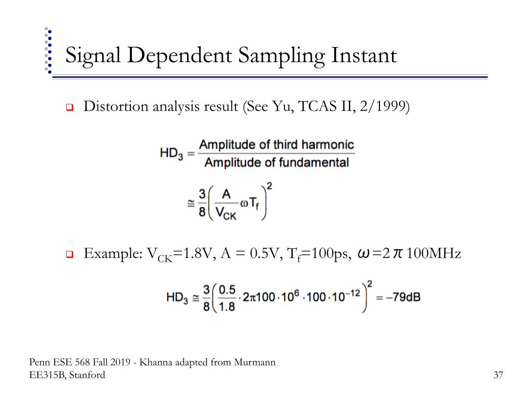
Signal Dependent Sampling Instant
! Distortion analysis result (See Yu, TCAS II, 2/1999)
! Example: VCK=1.8V, A = 0.5V, Tf=100ps, ω=2π100MHz
37 Penn ESE 568 Fall 2019 - Khanna adapted from Murmann EE315B, Stanford

Charge Injection and Clock Feedthrough
! Analyze two cases " Very Large Tf (slow-gating) " Very Small Tf (fast-gating)
38 Penn ESE 568 Fall 2019 - Khanna adapted from Murmann EE315B, Stanford

Slow Gating
! All channel charge has disappeared by toff without introducing error; absorbed by input source
39 Penn ESE 568 Fall 2019 - Khanna adapted from Murmann EE315B, Stanford

Slow Gating Model for t>toff
40 Penn ESE 568 Fall 2019 - Khanna adapted from Murmann EE315B, Stanford

Slow Gating Model for t>toff
41 Penn ESE 568 Fall 2019 - Khanna adapted from Murmann EE315B, Stanford

Slow Gating Model for t>toff
42 Penn ESE 568 Fall 2019 - Khanna adapted from Murmann EE315B, Stanford
! Example:

Fast Gating
! Channel charge cannot change instantaneously
! Resulting surface potential decays via charge flow to source and drain (charge injection)
! Charge divides between source and drain
43 Penn ESE 568 Fall 2019 - Khanna adapted from Murmann EE315B, Stanford

Charge Split Ratio
44 Penn ESE 568 Fall 2019 - Khanna adapted from Murmann EE315B, Stanford
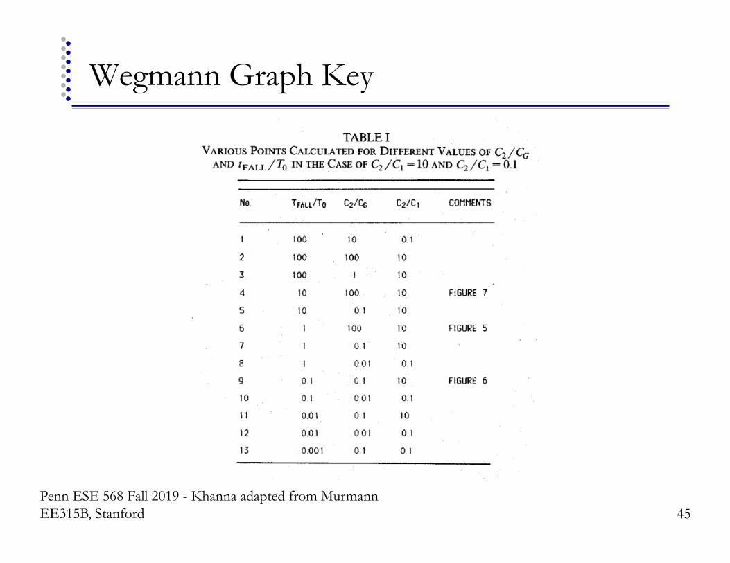
Wegmann Graph Key
45 Penn ESE 568 Fall 2019 - Khanna adapted from Murmann EE315B, Stanford

Interpretation
! This means that in practice split will have dependence on impedances seen on either side of transistors
! Remember: Slightly more charge will go to side with lower impedance (higher capacitance)
46 Penn ESE 568 Fall 2019 - Khanna adapted from Murmann EE315B, Stanford

Fast Gating Model for t>toff
47 Penn ESE 568 Fall 2019 - Khanna adapted from Murmann EE315B, Stanford

Fast Gating Model for t>toff
48 Penn ESE 568 Fall 2019 - Khanna adapted from Murmann EE315B, Stanford

Fast Gating Model for t>toff
49 Penn ESE 568 Fall 2019 - Khanna adapted from Murmann EE315B, Stanford

Fast Gating Model for t>toff
50 Penn ESE 568 Fall 2019 - Khanna adapted from Murmann EE315B, Stanford
! Example:

Fast Gating Model for t>toff
51 Penn ESE 568 Fall 2019 - Khanna adapted from Murmann EE315B, Stanford
! Example:
Slow gating

Transition Fast/Slow Gating
! |ε| and |VOS| decrease as the clock fall time increases and approaches the limit of slow gating
! Practical cases are closer to fast-gating side
52 Penn ESE 568 Fall 2019 - Khanna adapted from Murmann EE315B, Stanford

Impact of Technology Scaling
! Charge injection error to speed ratio benefits from short channels and increases in mobility
53 Penn ESE 568 Fall 2019 - Khanna adapted from Murmann EE315B, Stanford

Impact of Technology Scaling
! Charge injection error to speed ratio benefits from short channels and increases in mobility
54 Penn ESE 568 Fall 2019 - Khanna adapted from Murmann EE315B, Stanford

First order improvements
Penn ESE 568 Fall 2019 - Khanna adapted from Murmann EE315B, Stanford 55

Improvements
! CMOS switch " Try to balance nonidealities of nMOS with parallel pMOS
! Charge cancelation " Try to cancel charge injection with dummy switch
! Differential Sampling " Differential signaling to suppress offset
56 Penn ESE 568 Fall 2019 - Khanna adapted from Murmann EE315B, Stanford

Charge Cancellation: CMOS Switch
! Partial cancellation of offset error ! Assuming fast gating, 50/50 charge split and WnLn=WpLp
! Charges full cancel for Vin=(VH-VL)/2=VDD/2 and Vtn=-Vtp " Still signal dependent residual injection
57 Penn ESE 568 Fall 2019 - Khanna adapted from Murmann EE315B, Stanford

CMOS Switch Resistance
! In principle, adding PMOS helps with signal dependent Ron in track mode " Parallel resistance of MOS devices roughly constant
58 Penn ESE 568 Fall 2019 - Khanna adapted from Murmann EE315B, Stanford

Analysis
! Independent of Vin # too good to be true! ! Missing factors
" Backgate effect " Short channel effects
59 Penn ESE 568 Fall 2019 - Khanna adapted from Murmann EE315B, Stanford

Real CMOS Switch
! Design " Size P/N ratio to minimize change in R over input range
! PMOS bring limited benefit unless the input signal range is large or centered near VDD
60 Penn ESE 568 Fall 2019 - Khanna adapted from Murmann EE315B, Stanford

Charge Cancellation: Dummy Switch
! Cancellation is never perfect, since channel charge of M1 will not be 50/50 split " If Rs small, most of charge will flow toward the input voltage source " ~80% cancellation
! Not precision technique, just a partial clean-up attempt
61 Penn ESE 568 Fall 2019 - Khanna adapted from Murmann EE315B, Stanford
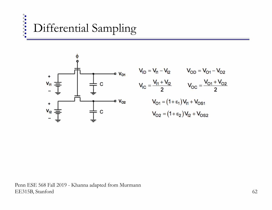
Differential Sampling
62 Penn ESE 568 Fall 2019 - Khanna adapted from Murmann EE315B, Stanford

Differential Sampling
63 Penn ESE 568 Fall 2019 - Khanna adapted from Murmann EE315B, Stanford

Differential Sampling
64 Penn ESE 568 Fall 2019 - Khanna adapted from Murmann EE315B, Stanford

Differential Sampling
! Assuming good matching between the two half circuits, we have all benefits of differential signaling " Small residual offset in VOD
" Good rejection of coupling noise, supply noise, … " Small common-mode to differential-mode gain
! Unfortunately, VOD has same gain error as basic single-ended circuit
! Also have nonlinear terms " Simplistic models assume channel charge linearly related
to Vin (ignoring higher order effects, e.g. backgate effect) " Expect to see nonlinear distortion along with gain error
65 Penn ESE 568 Fall 2019 - Khanna adapted from Murmann EE315B, Stanford

Big Ideas
! Elementary track-and-hold circuit and its nonidealities " Finite acquisition time " Tracking nonlinearity " Signal dependent hold instant
! First order improvements to elementary track-and-hold " Charge cancellation, CMOS switches, differential signals
66 Penn ESE 568 Fall 2019 - Khanna adapted from Murmann EE315B, Stanford

Admin
! Proj 1 " Due Su 10/6
! Turn in design with characterization even if you don’t meet all the specs
67 Penn ESE 568 Fall 2019 – Khanna adapted from Murmann EE315B, Stanford


