Download - FPGA Control of Coherent Pulse Stacking
FPGA Control of Coherent Pulse StackingYilun Xu1,2, Russell Wilcox1, John Byrd1, Larry Doolittle1, Qiang Du1, Gang Huang1, Yawei Yang1
1Lawrence Berkeley National Laboratory, Berkeley, CA 94720, USA2Department of Engineering Physics, Tsinghua University, Beijing 100084, China
Abstract
Coherent pulse stacking (CPS) is a new time-domain coherent addition technique that stacks several optical pulses into a single output pulse,enabling high pulse energy from fiber lasers. Due to advantages of precise timing and fast processing, we use an FPGA to process digitalsignals and do feedback control so as to realize stacking-cavity stabilization. We develop a hardware and firmware design platform to supportthe coherent pulse stacking application. A firmware bias control module stabilizes the amplitude modulator at the minimum of its transferfunction. A cavity control module ensures that each optical cavity is kept at a certain individually-prescribed and stable round-trip phase with2.5 deg rms phase error.
Introduction
I High laser pulse energy isachieved at low repetitionrate currently.
I CPS combines high averagepower and high repetitionrate.
I Joule-kHz CPS system willrevolutionize LPAs andFELs.
Hardware and Firmware InfrastructureHardware:I ML605 + FMC110 + XM105I 2-CH 12-bit A/D & 2-CH 16-bit D/A & 400MspsI kHz Feedback Control Repetition Rate
Firmware:I Bottom Layer: Hardware-Dependent DriversI Intermediate Layer: Data Communication Layer (UDP)
I Top Layer: Project Specific DSPI bias ctrl.vI cavity ctrl.v
Cavity Control
I Lock the cavity phase at the desired angle to realize coherent pulse stacking.I Cavity control module programs the slow DAC and drives the PZT to stabilize the optical cavity.I Three clock domain: sampling clock domain (400MHz), processing clock domain (50MHz),
feedback clock domain (kHz).
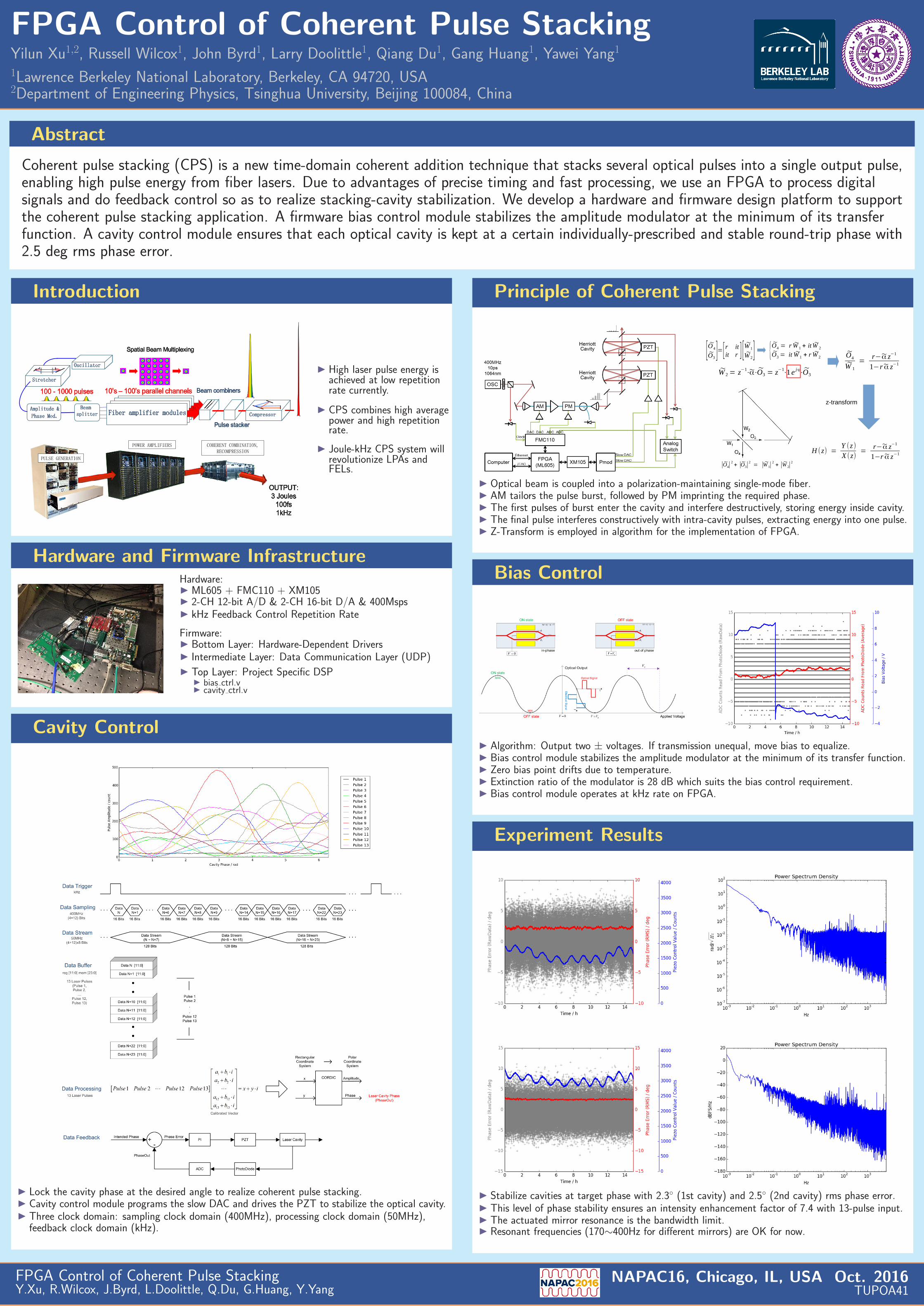
Principle of Coherent Pulse Stacking
[~O 4~O3 ]=[r it
it r ][~W 1~W 2
] {~O4 = r ~W 1 + it ~W 2~O3 = it ~W 1 + r ~W 2
|~O4|2+ |~O3|
2= |~W 1|
2+ |~W 2|
2
~W 2 = z−1⋅~α⋅
~O3 = z−1
⋅1e jϕ⋅~O3
~O4~W 1
=r−~α z−1
1−r~α z−1
H (z) =Y (z )X (z)
=r−~α z−1
1−r~α z−1
z-transform
I Optical beam is coupled into a polarization-maintaining single-mode fiber.I AM tailors the pulse burst, followed by PM imprinting the required phase.I The first pulses of burst enter the cavity and interfere destructively, storing energy inside cavity.I The final pulse interferes constructively with intra-cavity pulses, extracting energy into one pulse.I Z-Transform is employed in algorithm for the implementation of FPGA.
Bias Control
I Algorithm: Output two ± voltages. If transmission unequal, move bias to equalize.I Bias control module stabilizes the amplitude modulator at the minimum of its transfer function.I Zero bias point drifts due to temperature.I Extinction ratio of the modulator is 28 dB which suits the bias control requirement.I Bias control module operates at kHz rate on FPGA.
Experiment Results
I Stabilize cavities at target phase with 2.3◦ (1st cavity) and 2.5◦ (2nd cavity) rms phase error.I This level of phase stability ensures an intensity enhancement factor of 7.4 with 13-pulse input.I The actuated mirror resonance is the bandwidth limit.I Resonant frequencies (170∼400Hz for different mirrors) are OK for now.
FPGA Control of Coherent Pulse StackingY.Xu, R.Wilcox, J.Byrd, L.Doolittle, Q.Du, G.Huang, Y.Yang
NAPAC16, Chicago, IL, USA Oct. 2016TUPOA41


