
GP1S396HCP0F
1
Sheet No.: OP13018EN
Notice The content of data sheet is subject to change without prior notice.
In the absence of confirmation by device specification sheets, SHARP takes no responsibility for any defects that may occur in equipment using any SHARP
devices shown in catalogs, data books, etc. Contact SHARP in order to obtain the latest device specification sheets before using any SHARP device.
GP1S396HCP0F is a phototransistor output,
transmissive photointerrupter with a industry’s
smallest compact and low-profile package by the thin
molding technology. This product detects an object
between the emitter and the detector.
In addition, by narrowing the slit width of the infrared
beam to 0.12mm, this product has improved detection
accuracy.
1. Transmissive with phototransistor output
2. Highlights :
・Compact size
・Low Profile
・Narrow Gap
3. Key Parameters :
・Gap Width : 1.2mm
・Slit Width (detector side) : 0.12mm
・Package : 2.26 × 1.4 × 1.6mm
4. RoHS directive compliant
1. Compliant with RoHS directive (2002/95/EC)
1. General purpose detection of object presence or
motion.
Example : printer, lens control for camera,
various mechanical position detection
■Description
■Features
■Agency approvals/Compliance
■Applications
Gap : 1.2mm Slit : 0.12mm Phototransistor Output, Compact Transmissive Photointerrupter
GP1S396HCP0F

GP1S396HCP0F
2
Sheet No.: OP13018EN
■Internal Connection Diagram
■Outline Dimensions Drawing No. CY14940i02 Scale : 15/1 Unit : mm
Note
1) Unspecified tolerance shall be ± 0.08mm.
2) Dimensions in parenthesis are shown for reference.
3) The dimensions indicated by ※ refer to the those measured from the lead base.
4) The dimensions shown do not include those of burrs.
Burr’s dimensions shall be 0.15Max.
5) There is a possibility that the lead of part is exposed.
6) There is a possibility that the internal device is exposed at the top of the device because of the thin thickness
of the outer package.
7) The mark possibly adheres partially of the side.
8) The dimension size doesn’t contain the mark thickness.
A : Anode
K : Cathode
C : Collector
E : Emitter
Top View

GP1S396HCP0F
3
Sheet No.: OP13018EN
Soldering area
0.2mm or more from the bottom face of package
through the substrate.
10%
90%
Output
Input
tr tf
■Absolute maximum ratings Ta=25°C
Parameter Symbol Rating Unit
Input
Forward current IF 30 mA
Reverse voltage VR 6 V
Power dissipation P 50 mW
Output
Collector-emitter voltage VCEO 35 V
Emitter-collector voltage VECO 6 V
Collector current Ic 20 mA
Collector power dissipation Pc 50 mW
Total power dissipation Ptot 70 mW
Operating temperature Topr -25 to +85 °C
Storage temperature Tstg -40 to +100 °C
* Soldering temperature Tsol 300 °C
* Soldering time : 3 s or less (Hand solder.)
■Electro-optical Characteristics Ta=25°C
Parameter Symbol Conditions MIN. TYP. MAX. Unit
Input Forward voltage VF IF=20mA - 1.2 1.4 V
Reverse current IR VR=3V - - 10 μA
Output Collector dark current ICEO VCE=20V - - 100 nA
Transfer
character-
istics
Collector current Ic VCE=5V, IF=5mA 100 - 400 μA
Response time (Rise) tr VCE=5V, Ic=100μA
RL=1kΩ
- 30 120 μs
(Fall) tf - 30 120 μs
Collector-emitter
saturation voltage VCE(sat) IF=10mA, Ic=40μA - - 0.4 V
(Test circuit for response time)
Vcc
RL
Test pin

GP1S396HCP0F
4
Sheet No.: OP13018EN
-25 0 25 50 75 100 85
50
40
30
20
10
0 40
Ambient temperature Ta (°C)
Fo
rwar
d
curr
ent
(mA
) P
ow
er
dis
sip
atio
n
P,
P
c,
Pto
t (m
W)
Ambient temperature Ta (°C)
15
100 85 75 50 25 0 -25
0
40
50
70
20
Total power dissipation
Input and output power dissipation
Forward current vs. ambient temperature
Power dissipation vs. ambient temperature
5

GP1S396HCP0F
5
Sheet No.: OP13018EN
100
80
60
40
20
50
90
10
-1 1 0 2 3
Shield distance L (mm)
Rel
ativ
e co
llec
tor
curr
ent
(%
)
Sh
ield
d
ista
nce
L
Shield
-
+
0
Sensor Test condition
IF=5.0mA
VCE=5V
Ta=25°C
100
80
60
40
20
50
90
10
-1 1 0 2 3
Shield distance L (mm)
Rel
ativ
e co
llec
tor
curr
ent
(%
)
Relative collector current vs. shield distance 1 (Reference value)
Relative collector current vs. shield distance 2 (Reference value)
Test condition
IF=5.0mA
VCE=5V
Ta=25°C
Sh
ield
dis
tan
ce
L
Shield -
+
0
Sensor

GP1S396HCP0F
6
Sheet No.: OP13018EN
■Supplements
●ODS materials
This product shall not contain the following materials.
Also, the following materials shall not be used in the production process for this product.
Materials for ODS : CFCS, Halon, Carbon tetrachloride 1.1.1-Trichloroethane (Methyl chloroform)
●Halogen material
Chlorine < 900ppm , Bromine < 900ppm , Chlorine + Bromine < 1500ppm (Homogeneous material)
●Compliance with each regulation
1) The RoHS directive(2002/95/EC)
This product complies with the RoHS directive(2002/95/EC).
Object substances: mercury, lead, cadmium, hexavalent chromium, polybrominated biphenyls (PBB)
and polybrominated diphenyl ethers (PBDE)
2) Content of six substances specified in Management Methods for Control of Pollution Caused by Electronic
Information Products Regulation (Chinese : 电子信息产品污染控制管理办法).
Category
Toxic and hazardous substances
Lead
(Pb)
Mercury
(Hg)
Cadmium
(Cd)
Hexavalent
chromium
(Cr6+
)
Polybrominated
biphenyls
(PBB)
Polybrominated
diphenyl ethers
(PBDE)
Photointerrupter ✓ ✓ ✓ ✓ ✓ ✓
✓: indicates that the content of the toxic and hazardous substance in all the homogeneous materials of the part is
below the concentration limit requirement as described in SJ/T 11363-2006 standard.
●Product mass : Approx. 6mg
●Country of origin : China
●Taping specification : Refer to the attachment-1.

GP1S396HCP0F
7
Sheet No.: OP13018EN
0.86mm or more 0.86mm or more
■Notes
●Circuit design
In circuit designing, make allowance for the degradation of the light emitting diode output that results
from long continuous operation. (50% degradation/5 years)
●Prevention of detection error
To prevent photointerrupter from faulty operation caused by external light, do not set the detecting face to the
external light.
●Position of opaque board
Opaque board shall be installed at place 0.86mm or more from the top of elements.
(Example)
●Soldering
Hand soldering
Please solder to each lead pin at 0.2mm or more from the bottom face of package through the substrate at 300°C
for 3 seconds or less.
Please don't bend lead pins from the root of package when soldering.
And please take care not to apply outer force to both lead pins and the package.
Please don't do soldering with preheating, and please don't do soldering by reflow.
In case of repairing, please make sure GP1S396HCP0F is cooled down, please consider the outer mold resin
is meltdown in case a continuous heat is applied.
Since the tip of the lead has exposed lead frame base material, there is a case not to be soldered.
●Cleaning
Cleaning shall be carried out under the below conditions to avoid keeping solvent, solder and flux on the device.
(1) Solvent cleaning : Solvent temperature 45°C or less, Immersion for 3 min. or less
(2) Ultrasonic cleaning : Since the influence to the product may changes by the conditions of the ultrasonic
power, time, the tank size, PCB size, the product installation condition, etc., please evaluate with actual
conditions and confirm before usage.
(3) The cleaning shall be carried out with solvent below.
Solvent : Ethyl alcohol, Methyl alcohol
●Lead pin
Lead terminals of this product have Copper, Nickel, Palladium and Gold plating.
Before usage, please evaluate solder ability with actual conditions and confirm.
The uniformity in color for the lead terminals are not specified.
●Storage and management after open
Storage condition : Storage shall be in accordance with the below conditions.
Storage temp. : 5 to 30°C
Storage humidity : 70%RH or less

GP1S396HCP0F
8
Sheet No.: OP13018EN
■Parts
This product uses the below parts.
● Light detector (Quantity : 1)
Type Material Maximum sensitivity
(nm)
Sensitivity
(nm)
Response time
(μs)
Phototransistor Silicon
(Si) 920 700 to 1200 20
● Light emitter (Quantity : 1)
Type Material Maximum light emitting
wavelength (nm)
I/O Frequency
(MHz)
Infrared light emitting diode
(non-coherent) GaAs 940 0.3
● Material
Case Lead frame Lead frame plating
Black PPA resin 42 Alloy Au-Pd-Ni-Cu
● Others
This product shall not be proof against radiation flux.

GP1S396HCP0F
9
Sheet No.: OP13018EN
■Packing Drawing No. CY14941i09
● Inner Packing
1) Inner Packaging drawing
2) Inner Packing material : ・Reel(PS) ・Carrier tape(PC) ・Caver tape(PET)
3) Quantity : 2,800pcs./Reel
● Outer Packaging
1) Outer Packaging drawing
2) Outer Packing material : Packing case(Corrugated cardboard), Cushioning material(Urethane)
Label(paper), Tape
3) Quantity : 14,000pcs./box
4) The contents of the carton indication conforms to EIAJ C-3 and the following items are indicated.
Model No., Internal production control name, Quantity, Packing date, Corporate name, Country of origin
5) Regular packaged mass : Approximately 500g

GP1S396HCP0F
10
Sheet No.: OP13018EN
(Attachment-1-1)
Package specifications (φ180mm reel)
1) Application
This specification applies to the taping specifications and the relation items for the GP1S396HCP0F.
2) Taping method
(1) Tape structure and Dimensions (Refer to the attached sheets-1-2)
The tape shall have a structure in which a cover tape is sealed pressed on the carrier tape made by
polycarbonate to protect against static electricity.
(2) Reel structure and Dimensions (Refer to the attached sheets-1-3)
(3) Direction of product insertion (Refer to the attached sheets-1-3)
Product direction in carrier tape shall direct to the detector at the hole side on the tape.
3) Repair method of sealing error
In case of repairing a sealing error, three sides of a cover tape matching to the product insertion portion are
opened by a cutter and it will be closed by adhesiveness tape after repairing.
4) Adhesiveness of cover tape
The exhalation force between carrier tape and cover tape shall be 0.1N to 1.0N for the angle from 165° to 180°.
5) Rolling method and quantity
(1) Wind the tape back on the reel so that the cover tape will be outside the tape.
(2) Attach more than 16cm of blank tape to the trailer and attach more than 10cm of the leader.
Attach more than 40cm of cover tape to the leader to the tape and fix the both ends with adhesive tape.
(3) One reel shall contain 2,800 pcs.
6) Indication items
The contents of the carton indication conforms to EIAJ C-3 and the following items are indicated.
Model No., Internal production control name, Quantity, Packing date, Corporate name, Country of origin
7) Safety protection during shipping
There shall be no deformation of component or degradation of electrical characteristics due to shipping.
GP1S396HCP0F
11
Sheet No.: OP13018EN
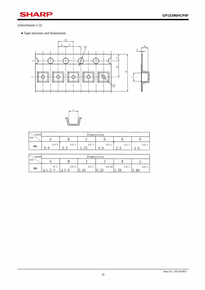
(Attachment-1-2)
● Tape structure and dimensions

GP1S396HCP0F
12
Sheet No.: OP13018EN
(Attachment-1-3)
● Reel structure and dimensions
● Direction of product insertion

GP1S396HCP0F
13
Sheet No.: OP13018EN
■Important Notices
· The circuit application examples in this publication are provided
to explain representative applications of SHARP devices and are
not intended to guarantee any circuit design or license any
intellectual property rights. SHARP takes no responsibility for
any problems related to any intellectual property right of a third
party resulting from the use of SHARP's devices.
· Contact SHARP in order to obtain the latest device specification
sheets before using any SHARP device. SHARP reserves the
right to make changes in the specifications, characteristics, data,
materials, structure, and other contents described herein at any
time without notice in order to improve design or reliability.
Manufacturing locations are also subject to change without
notice.
· Observe the following points when using any devices in this
publication. SHARP takes no responsibility for damage caused
by improper use of the devices which does not meet the
conditions and absolute maximum ratings to be used specified in
the relevant specification sheet nor meet the following
conditions:
(i) The devices in this publication are designed for use in general
electronic equipment designs such as:
--- Personal computers
--- Office automation equipment
--- Telecommunication equipment [terminal]
--- Test and measurement equipment
--- Industrial control
--- Audio visual equipment
--- Consumer electronics
(ii) Measures such as fail-safe function and redundant design
should be taken to ensure reliability and safety when SHARP
devices are used for or in connection
with equipment that requires higher reliability such as:
--- Transportation control and safety equipment (i.e.,
aircraft, trains, automobiles, etc.)
--- Traffic signals
--- Gas leakage sensor breakers
--- Alarm equipment
--- Various safety devices, etc.
(iii) SHARP devices shall not be used for or in connection with
equipment that requires an extremely high level of reliability and
safety such as:
--- Space applications
--- Telecommunication equipment [trunk lines]
--- Nuclear power control equipment
--- Medical and other life support equipment (e.g.,
scuba).
· If the SHARP devices listed in this publication fall within the
scope of strategic products described in the Foreign Exchange
and Foreign Trade Law of Japan, it is necessary to obtain
approval to export such SHARP devices.
· This publication is the proprietary product of SHARP and is
copyrighted, with all rights reserved. Under the copyright laws,
no part of this publication may be reproduced or transmitted in
any form or by any means, electronic or mechanical, for any
purpose, in whole or in part, without the express written
permission of SHARP. Express written permission is also
required before any use of this publication may be made by a
third party.
· Contact and consult with a SHARP representative if there are
any questions about the contents of this publication.


