BULLETIN OF THE POLISH ACADEMY OF SCIENCES
TECHNICAL SCIENCES
Vol. 57, No. 4, 2009
High efficiency contactless energy transfer system
with power electronic resonant converter
A.J. MORADEWICZ1 and M.P. KAZMIERKOWSKI2∗
1 Electrotechnical Institute IEl, 28 M. Pożaryskiego St., 04-703 Warsaw, Poland2 Institute of Control and Industrial Electronics, Warsaw University of Technology, 75 Koszykowa St., 00-662 Warsaw, Poland
Abstract. A novel Inductive Contactless Energy Transfer (ICET) system is presented in this paper. The energy is transferred using a rotatable
air gap transformer and a power electronic converter. To minimize total losses of the system a series resonant circuit is applied, assuring zero
current switching condition for IGBT power transistors. The analytical expression of the transfer dc voltage gain is given and discussed. The
developed ICET system is characterized by high efficiency and fast FPGA based controller and protection system. The resonant frequency is
adjusted by extreme regulator which follows instantaneous value of primary peak current. Simulated and experimental results which verify
and illustrate operation of developed 3 kW laboratory model are presented.
Key words: inductive contactless energy transfer, series resonant converter, FPGA control.
1. Introduction
The contactless energy transfer systems have been recently
gaining popularity and investigated widely [1–16]. This inno-
vative technology creates new possibilities to supply mobile
devices with electrical energy because elimination of cables,
and/or slip-rings as well as plugs and sockets increases relia-
bility and maintenance-free operation of such critical systems
as in aerospace, biomedical, electric vehicles and robotics ap-
plications. The core of contactless energy transfer system is
inductive or capacitive coupling and high switching frequen-
cy power electronic converter. The capacitive coupling is used
in low power range (sensor supply systems) whereas induc-
tive coupling allows transferring power from a few mW up to
hundred kW [1, 4].
This paper reports on a new developed Inductive Contact-
less Energy Transfer (ICET) system with a rotatable air gap
transformer and IGBT transistors based resonant power elec-
tronic converter. Thanks to the careful design of all system-
components, the high total efficiency (93%) is achieved. Other
important features of the presented ICET system are: opera-
tion of high-switching frequency IGBT transistor based res-
onant converter at zero current switching (ZCS) conditions,
low cost single board FPGA based controller, reliable and fast
operation, robustness to magnetic coupling factor changes of
the main circuit. Simulation and experimental results of 3kW
prototype system operated with 60 kHz switching frequency
are presented.
2. Topology of Inductive contactless energy
transfer (ICET) system
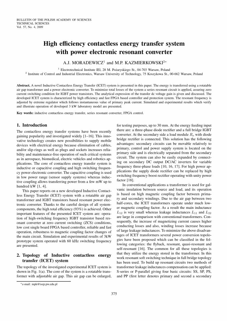
The topology of the investigated experimental ICET system is
shown in Fig. 1(a). The core of the system is a rotatable trans-
former with adjustable air gap. This air gap can be enlarged,
for testing purposes, up to 30 mm. At the energy feeding input
there are: a three-phase diode rectifier and a full bridge IGBT
converter. At the secondary side a load module Ro with diode
bridge rectifier is connected. This solution has the following
advantages: secondary circuits can be movable relatively to
primary, control and power supply system is located on the
primary side and is electrically separated from the secondary
circuit. The system can also be easily expanded by connect-
ing on secondary DC output DC/AC inverters for variable
frequency three-phase loads [10, 16, 17]. For high power ap-
plications the supply diode rectifier can be replaced by high
switching frequency boost rectifier operating with unity power
factor [18].
In conventional applications a transformer is used for gal-
vanic insulation between source and load, and its operation
is based on high magnetic coupling factor between prima-
ry and secondary windings. Due to the air gap between two
half-cores, the ICET transformers operate under much low-
er magnetic coupling factor. As a result the main inductance
L12 is very small whereas leakage inductances L11 and L22
are large in comparison with conventional transformers. Con-
sequently, the increase of magnetizing current causes higher
conducting losses and also, winding losses increase because
of large leakage inductances. To minimize the above disadvan-
tages of ICET transformers several power conversion topolo-
gies have been proposed which can be classified in the fol-
lowing categories: the flyback, resonant, quasi-resonant and
self-resonant [16]. The common for all these topologies is
that they utilize the energy stored in the transformer. In this
work resonant soft switching technique in full bridge topology
has been used. To build up resonant circuits two methods of
transformer leakage inductances compensation can be applied:
S-series or P-parallel giving four basic circuits: SS, SP, PS,
and PP (first letter denotes primary and second a secondary
∗e-mail: [email protected]
375
A.J. Moradewicz and M.P. Kazmierkowski
a)
b)
Fig. 1. (a) Circuit topology of developed Inductive Contactless Energy Transfer (ICET) system, (b) Equivalent circuit for fundamental
harmonic
compensation). PS and PP require an additional series induc-
tor to regulate the inverter current flowing into the parallel
resonant circuit. This additional inductor increases Electro-
Magnetic Compatibility (EMC) problems and total cost of
ICET system. Therefore, only SS and SP circuits have been
considered.
3. Analysis of compensation circuits
Assuming the same numbers of primary and secondary wind-
ing N1 = N2, the inductances of presented transformer can
be described as follows:
L1 = L11 + L12
L2 = L22 + n2L12
M = nL12
⇒
L1 = L11 + L12
L2 = L22 + L12
M = L12
(1)
whereL1 = L2 = L,
L11 = L22 = L − M =1 − k
kM,
k = M/L, n =N2
N1.
(2)
If the fundamental component of u2 (t) is in phase with i2 (t),the output rectifier with capacitive filter behaves as load resis-
tance transformer. The value of this resistance is equal to [1]:
Res =8U0
π2I0= 0.8106 · Ro. (3)
Impedance of secondary side in case of chosen compensation
circuits is:
– for series compensation:
Zγ = Res + jX2, (4)
– for parallel compensation:
Zγ =
jωL11 + 1/
(
jω · Cr2 +1
Rep
)
. (5)
The equations for component impedance and reactance,
shown at various points in Fig. 1(b) can be written as:
Zβ =jXm · Zγ
jXm + Zγ
(6)
Zα = jX1 + Zβ, (7)
X1 = ωsL11 −1
ωsCr1, (8)
X2 = ωsL22 −1
ωsCr2, (9)
Xm = ωsM, (10)
where ωs = 2πfs – operation inverter frequency.
376 Bull. Pol. Ac.: Tech. 57(4) 2009

High efficiency contactless energy transfer system with power electronic resonant converter
The voltage transfer function of ICET system for SS compen-
sation circuits in Fig. 1(b) is:
GV =
∣
∣
∣
∣
Zβ
Zα
Res
Zγ
∣
∣
∣
∣
. (11)
From Eqs. (3) to (11), the resulting equation of the transfer
gain GV express as:
GV =
(
1 +X1
Xm
)2
+
X1 + X2 +X1 · X2
Xm
Res
2
− 1
2
.
(12)
From Eq. (12) follows that GV is unity at compensated fre-
quency, even though the leakage inductances of the rotating
transformer in ICET system are very large. Where ω0 = 2πf0
– resonant frequency – (compensated frequency), is derived
for condition X1 = X2 = 0
ωo = 1/√
LrCr = 1/√
L11CR1 = 1/√
L22CR2. (13)
Based on Eqs. (7, 8 and 13) the expression for X1 and X2
can be rewritten by:
X1 = ωsL11
(
1 −1
ω2
)
, (14)
X2 = ωsL22
(
1 −1
ω2
)
, (15)
where
ω = ωs/ωo. (16)
Because of used two half-cores and large air gap, the
ICET transformer operates under low and variable magnet-
ic coupling factor k. Therefore, the voltage gain GV can be
expressed in terms of coupling factor k. For simplification
we assume that the configurations of primary and secondary
transformer windings are identical. From Eqs. (12) to (16) the
voltage gain function can be rewritten as:
GV =s1+
1−k
k
1−
1
ω2
2
+
Qac
ω−
1
ω
1+
1 − k
2k
1−
1
ω2
2
,
(17)
where circuit quality factor for SS compensation topology is:
Qac =ω (L11 + L22)
Res
=ωLr
Res
. (18)
The analytical results of the voltage gain function based
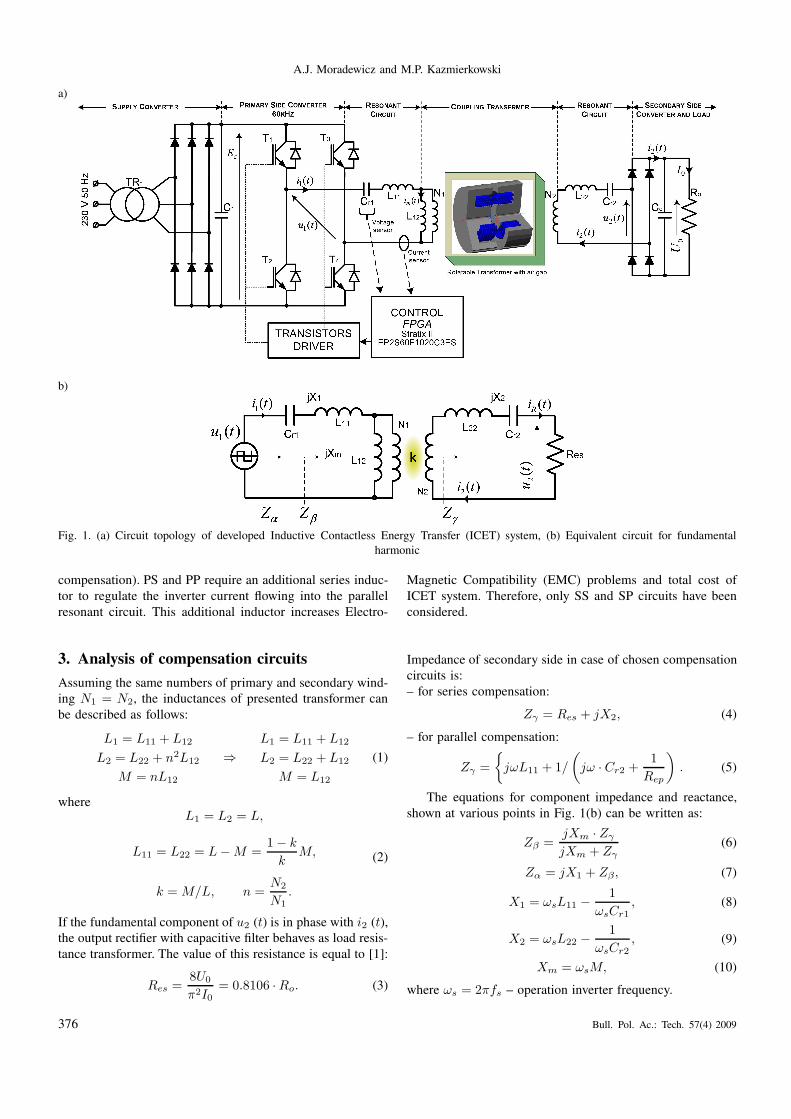
on Eq. (17) are illustrated in Fig. 2. The calculations were per-
formed versus the normalized angular frequency ω, for two
values of coupling factor k and various Qac as parameter. It
can be seen that the curves of voltage transfer function GV
for k = 0.2 and 0.8 are similar except for a small deviation
in low circuit quality factor Qac. For the output-voltage reg-
ulation, the feedback control should be applied selecting the
desirable operation range from three different regions A, Band C of the voltage transfer function GV presented in Fig. 2.
Regions A or C are able to unambiguous control the output
voltage since the GV is a monotonic function of switching fre-
quency. The range C is favorable because the voltage transfer
function for each load conditions is much less sensitive than
in the Range A. Moreover, when increasing switching fre-
quency, the changes in output voltage are very fast. This fact
is important in control system, for example when dangerous
state is detecting (ωs < ωo).
a)
b)
Fig. 2. Illustration of transfer dc voltage gain Gv versus normalized
frequency in ICET system for SS compensation circuit. a) k = 0.2,
b) k = 0.8
The required resonant capacitors values for desired reso-
nant frequency can be expressed as follows:
– for series secondary compensation
Cr1 =L22
L11Cr2 = Cr2|L11=L22
, (19)
– for parallel secondary compensation
Cr1 =L2
22 · Cr2
L11 · L22−(k · L11 · L22)2 = |L11=L22 | =
1
1 − k2Cr2.
(20)
Bull. Pol. Ac.: Tech. 57(4) 2009 377
A.J. Moradewicz and M.P. Kazmierkowski
An important advantage of SS compensation circuit is that
primary capacitance is independent of either magnetic cou-
pling factor or the load. In contrast the SP circuit depends on
coupling factor and requires higher value of capacitance for
stronger magnetic coupling.
4. Control and protection scheme
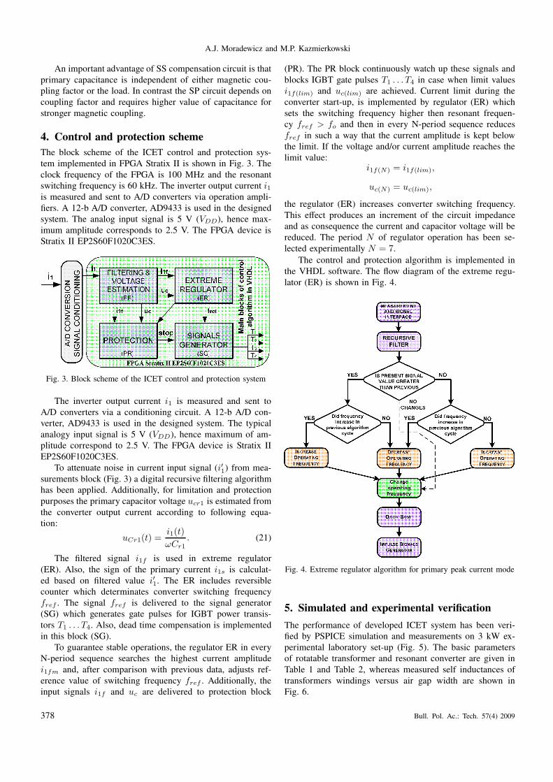
The block scheme of the ICET control and protection sys-
tem implemented in FPGA Stratix II is shown in Fig. 3. The
clock frequency of the FPGA is 100 MHz and the resonant
switching frequency is 60 kHz. The inverter output current i1is measured and sent to A/D converters via operation ampli-
fiers. A 12-b A/D converter, AD9433 is used in the designed
system. The analog input signal is 5 V (VDD), hence max-
imum amplitude corresponds to 2.5 V. The FPGA device is
Stratix II EP2S60F1020C3ES.
Fig. 3. Block scheme of the ICET control and protection system
The inverter output current i1 is measured and sent to
A/D converters via a conditioning circuit. A 12-b A/D con-
verter, AD9433 is used in the designed system. The typical
analogy input signal is 5 V (VDD), hence maximum of am-
plitude correspond to 2.5 V. The FPGA device is Stratix II
EP2S60F1020C3ES.
To attenuate noise in current input signal (i′1) from mea-
surements block (Fig. 3) a digital recursive filtering algorithm
has been applied. Additionally, for limitation and protection
purposes the primary capacitor voltage ucr1 is estimated from
the converter output current according to following equa-
tion:
uCr1(t) =i1(t)
ωCr1. (21)
The filtered signal i1f is used in extreme regulator
(ER). Also, the sign of the primary current i1s is calculat-
ed based on filtered value i′1. The ER includes reversible
counter which determinates converter switching frequency
fref . The signal fref is delivered to the signal generator
(SG) which generates gate pulses for IGBT power transis-
tors T1 . . . T4. Also, dead time compensation is implemented
in this block (SG).
To guarantee stable operations, the regulator ER in every
N-period sequence searches the highest current amplitude
i1fm and, after comparison with previous data, adjusts ref-
erence value of switching frequency fref . Additionally, the
input signals i1f and uc are delivered to protection block
(PR). The PR block continuously watch up these signals and
blocks IGBT gate pulses T1 . . . T4 in case when limit values
i1f(lim) and uc(lim) are achieved. Current limit during the
converter start-up, is implemented by regulator (ER) which
sets the switching frequency higher then resonant frequen-
cy fref > fo and then in every N-period sequence reduces
fref in such a way that the current amplitude is kept below
the limit. If the voltage and/or current amplitude reaches the
limit value:i1f(N) = i1f(lim),
uc(N) = uc(lim),
the regulator (ER) increases converter switching frequency.
This effect produces an increment of the circuit impedance
and as consequence the current and capacitor voltage will be
reduced. The period N of regulator operation has been se-
lected experimentally N = 7.
The control and protection algorithm is implemented in
the VHDL software. The flow diagram of the extreme regu-
lator (ER) is shown in Fig. 4.
Fig. 4. Extreme regulator algorithm for primary peak current mode
5. Simulated and experimental verification
The performance of developed ICET system has been veri-
fied by PSPICE simulation and measurements on 3 kW ex-
perimental laboratory set-up (Fig. 5). The basic parameters
of rotatable transformer and resonant converter are given in
Table 1 and Table 2, whereas measured self inductances of
transformers windings versus air gap width are shown in
Fig. 6.
378 Bull. Pol. Ac.: Tech. 57(4) 2009

High efficiency contactless energy transfer system with power electronic resonant converter
Fig. 5. View of laboratory setup of 3kW contactless power supply
system with rotatable transformer and series resonant IGBT inverter
Table 1
Parameters of rotatable transformer and resonant circuit
Parameter Value Unit
N1 and N2 32 coils
L11 166.5 µH
L12 203.5 µH
L22 166.5 µH
M 203.5 µH
k 0.55 –
CR1 and CR2 63 nF
Air gap 10.5 mm
Table 2
Parameters of resonant converter
Parameter Value Unit
Power Module SKM100GB124D
Voltage 1200 V
Current 150 A
Dead Time 1 µs
C1 1000 µF
CR1 63 nF
CR2 63 nF
CO 100 µF
Fig. 6. Measured self inductance primary and secondary winding of
rotating transformer in laboratory model
Fig. 7. Efficiency versus air gap width of the experimental ICET
system
Figure 7 shows total dc-dc measured input-output effi-
ciency of the ICET laboratory model system versus trans-
former air gap width and the load resistance. Note, that
for higher load resistances, in both compensation circuits,
higher efficiency is achieved. However, the efficiency of
ICET system with SP compensation is about 10% low-
er then with SS circuit, for the same circuit parame-
ters.
Figures 8 and 9 show PSPICE simulated and experimental
measured oscillograms of basic waveforms in the steady-state
operation of resonant converter. The load resistance was 10 Ωand transformer air gap width 3 and 25.5 mm in Fig. 8a and
Fig. 9, respectively. Operation mode above resonant frequency
for 3 mm transformer air gap width is shown in Fig. 8b. Note
that at resonant frequency power IGBT transistors operate at
Zero Current Switching (ZCS) conditions and power factor
achieves a value of 0.912 for power level 2.52 kW (Fig. 9).
Above resonant frequency (Fig. 8b) power transistor operate
at non ZCS conditions, with low power factor value of 0.279
and power level 137 W. The power flow is controlled by de-
tuned operation.
Investigation of operation at resonant frequency with dif-
ferent transformer air gap width has shown that system is well
synchronized by extreme regulator and operates properly for
magnetic coupling factor changes from 0.2 till 0.8.
Note that for higher load resistances higher efficiency can
be achieved, but the circuit becomes more sensitive to mag-
netic coupling factor changes.
Bull. Pol. Ac.: Tech. 57(4) 2009 379

A.J. Moradewicz and M.P. Kazmierkowski
Fig. 8. Converter operation at steady-state: a) at resonant frequency, b) above resonant frequency. From the top: voltages u1, u2, currents
i1, i2 and primary side power P1. Air gap length 3 mm, load resistance 10 Ω
a) b)
Fig. 9. Converter operation at steady-state: a) at resonant frequency, b) above resonant frequency. From the top: voltages u1, u2, currents
i1, i2 and primary side power P1. Air gap length 25.5 mm, load resistance 10 Ω
6. Conclusions
This paper presents an Inductive Contactless Energy Trans-
fer (ICET) system with rotatable air gap transformer and se-
ries resonant power electronic converter operating at 60 kHz
switching frequency.
The control and the protection system have been imple-
mented in FPGA Stratix II EP2S60F family. To compensate
for high leakage inductance of the rotatable transformer when
a large air gap is used and to minimize converter switch-
ing losses, the series resonant capacitive circuit has been
used in primary and secondary side. The resonant frequen-
cy is adjusted by extreme regulator which follows the instan-
taneous value of primary peak current and guaranties zero
current switching (ZCS) conditions for power IGBT transis-
tors of the inverter. This reduces switching losses consid-
380 Bull. Pol. Ac.: Tech. 57(4) 2009

High efficiency contactless energy transfer system with power electronic resonant converter
erably and increase overall system efficiency. Theoretically,
there is no power transfer limit, even with low magnetic cou-
pling factor, if the system operates at the resonant frequen-
cy of secondary current, with compensated primary wind-
ing conditions. Additionally, resonant frequency of primary
current should by equal to secondary. From (19) it can be
concluded that in SS compensation topology both resonant
capacitances are equal, if L11 = L22. The design proce-
dure has been verified by simulation and experimental re-
sults measured on the 3 kW laboratory set-up. The total ef-
ficiency achieves 93% for transformer with 10 mm air gap
width.
The developed ICET with a rotatable transformer is con-
structed mainly for robotics and manipulators, however, the
described design and control methodology has a general va-
lidity and can be applied for a wide class of contactless power
supply with core or core-less transformers.
REFERENCES
[1] Ch. Apneseth, D. Dzung, S. Kjesbu, G. Scheible, and W. Zim-
mermann, “Introduction wireless proximity switches”, ABB Re-
view 4, 42–49 (2002).
[2] A. Esser and H.Ch. Skudelny, “A new approach to power sup-
ply for robots”, IEEE Trans. on Ind. Applications 27 (5), 872–
875 (1991).
[3] J. Hirai, T.W. Kim, and A. Kawamura, “Study on intelligent
battery charging using inductive transmission of power and in-
formation”, IEEE Trans. on Power Electronics 15, 2, 335–344
(2000).
[4] M. Jufer, “Electric drive system for automatic guided vehi-
cles using contact-free energy transmission”, Electrotechnical
Review 84 (9), 35–39 (2008), (in Polish).
[5] J. Lastowiecki and P. Staszewski, “Sliding transformer with
long magnetic circuit for contactless electrical energy delivery
to mobile receivers, IEEE Trans. on Industrial Electronics 53,
6, 1943–1948 (2006).
[6] J.T. Matysik, “A new method of integration control with in-
stantaneous current monitoring for class D”, IEEE Trans. on
Industrial Electronics 53, 5, 1561–1576 (2006).
[7] R. Mecke and C. Rathage, “High frequency resonant converter
for contactless energy transmission over large air gap”, Proc.
IEEE-PESC 1, 1737–1743 (2004).
[8] R. Miśkiewicz and A. Moradewicz, “Contactless power supply
for notebooks”, Electrotechnical Review 85 (3), 8–14 (2009),
(in Polish).
[9] A. Moradewicz, “Contactless energy transmission system with
rotatable transformer – modeling, analyze and design”, PhD-
Thesis, Electrotechnical Institute (IEl), Warsaw, Poland, 2008.
[10] A. Moradewicz, “Study of wireless energy transmission sys-
tems using inductive coupling”, Proc. Int. Conf. PELINCEC,
CD-ROM (2005).
[11] A. Moradewicz and M.P. Kazmierkowski, “Resonant converter
based contactless power supply for robots and manipulators”,
J. Automation, Mobile Robotics & Intelligent Systems 2 (3),
20–25 (2008).
[12] K. O’Brien, G. Scheible, and H. Gueldner, “Analysis of wire-
less power supplies for industrial automation systems”, Proc.
IEEE Industrial Electronics Conf. IECON, CD-ROM (2003).
[13] Ch-S. Wang, O.H. Stielau, and G.A. Covic, “Design consid-
erations for contactless electric vehicle battery charger”, IEEE
Trans. on Industrial Electronics 52 (5), 1308–1313 (2005).
[14] Z. Chen, X. Zhang, and J. Pan, “An integrated inverter for a
single-phase single-stage grid connected PV system based on
Z-source”, Bull. Pol Ac.: Tech. 55 (3), 263–272 (2007).
[15] Z. Kaczmarczyk, “A novel phase-shift full-bridge converter
with voltage-doubler and decoupling integrated magnetics in
PV system”, Bull. Pol Ac.: Tech. 56 (3), 285–293 (2008).
[16] W. Erickson, Fundamentals of Power Electronics, Kluwer Aca-
demic Publisher, New York, 1999.
[17] Y. Jiang, Z. Chen, J. Pan, X. I. Zhao, and P. Lee, “A novel
phase-shift full-bridge converter with voltage-doubler and de-
coupling integrated magnetics in PV system”, Bull. Pol Ac.:
Tech. 56 (3), 285–293 (2008).
[18] P. Antoniewicz and M.P. Kazmierkowski, “Predictive direct
power control of three-phase boost rectifier”, Bull. Pol Ac.:
Tech. 54 (2), 447–454 (2006).
Bull. Pol. Ac.: Tech. 57(4) 2009 381


