
High Performance VLSI Architecture
for Digital FIR Filter Design
THESIS
Submitted in partial fulfillment
of the requirements for the degree of
DOCTOR OF PHILOSOPHY
by
SRINIVASA REDDY K
Under the supervision of
Dr. Subhendu Kumar Sahoo
BIRLA INSTITUTE OF TECHNOLOGY & SCIENCE
PILANI – 333 031 (RAJASTHAN) INDIA
2015

High Performance VLSI Architecture
for Digital FIR Filter Design
THESIS
Submitted in partial fulfillment
of the requirements for the degree of
DOCTOR OF PHILOSOPHY
by
SRINIVASA REDDY K
ID.No. 2007PHXF430P
Under the supervision of
Dr. Subhendu Kumar Sahoo
BIRLA INSTITUTE OF TECHNOLOGY & SCIENCE
PILANI – 333 031 (RAJASTHAN) INDIA
2015

BIRLA INSTITUTE OF TECHNOLOGY AND SCIENCE
PILANI (RAJASTHAN) INDIA
CERTIFICATE
This is to certify that the thesis entitled “High Performance VLSI Architecture for
Digital FIR Filter Design” and submitted by Mr. K Srinivasa Reddy, ID No.
2007PHXF430P for award of Ph.D. degree of the institute embodies original work done
by him under my supervision.
Signature of the Supervisor
Name : Dr. SUBHENDU KUMAR SAHOO
Designation : Assistant Professor
Department of Electrical & Electronics Engineering
BITS – Pilani, Hyderabad Campus
Date: ______________

Dedicated
to
My Family
Acknowledgements
I wish to express my heart-felt gratitude and sincere thanks to my thesis supervisor
Prof. Subhendu Kumar Sahoo, Department of Electrical and Electronics Engineering,
BITS-Pilani, Hyderabad Campus for his able guidance, encouragement and continued
support throughout the period of this research work. I have a deep sense of admiration
to his innate goodness. It has been a divine grace and my proud privilege for me to
work under his guidance.
I am indebted to Prof. V. S. Rao, Vice-Chancellor, Prof. Ashoke Kumar Sarkar,
Director, Prof. G Sundar, Director, Off-Campus Programme, Prof. S. K. Verma,
Dean, Academic Research Division, BITS, Pilani Campus for giving me an opportu-
nity to carry out research at the Institute.
I wish to express my deep sense of gratitude to the members of Doctoral Advisory
Committee (DAC), Prof. S. Gururnarayan and Prof. Sudeept Mohan, BITS-Pilani
for their constructive criticism, valuable suggestions and moral support throughout
the research work. Their editorial miracles of revision are simply amazing, without
which the thesis would have not taken right shape.
My sincere thanks to Prof. Anu Gupta, Head of department Electrical & Elec-
tronics Engineering, BITS-Pilani, for her encouragement, and moral support during
various phases of research work.
I am grateful for the best wishes and prayers of my friends cum colleagues Prof.
V.K Choube, Prof. Surekha Bhanot, Prof. Dheerendra Singh, Prof. H. D. Mathur,
Prof. Hari Om Bansal, Prof. Rajneesh Kumar, Prof. Navneet Gupta, Dr. Srinivas
Kota, Dr. Rahul Singhal, Dr. Nitin Chaturvedi, Dr. Ananthakrishna Chintanpalli
and Mr. Ananda Kumar A.
I express my heart-felt thanks to my friend cum colleague Mr. Pawan Sharma, for
his valuable suggestions and support for accessing the OLAB and EDA tools during
my research work.
ii

Special thanks to Mr. Giridhar Kunkur, Librarian, BITS-Pilani for making timely
availability of various books and on-line journals.
A very special and sincere heartfelt gratitude to my parents, Mr. Kotha Hanu-
mantha Rami Reddy and Mrs. Kotha Nagamaneswari, to my son Devesh and to my
wife Mrs. Sirisha, whose constant persuasion and moral support have been a source
of inspiration to me. No words can adequately express my gratitude to them.
iii

Abstract
Finite impulse response (FIR) filters are the basic building blocks of many digital
signal processing applications. The FIR filter receives a discrete time signal as input
and performs the multiplication and addition operations to give the desired filtered
discrete time output signal. The real time applications such as radar signal pro-
cessing and video processing, require dedicated hardware efficient FIR filters to be
implemented with higher clock frequencies. Nowadays, many battery operated de-
vices such as hearing aids and mobile phones also use FIR filters as it offers stability
and linear phase response. As these devices are power hungry devices, a low power
FIR implementation is required for these applications. Hence, to meet the ever de-
manding high speed and low power devices, new methods for hardware efficient FIR
filter architectures are proposed in this thesis. The FIR filter implementations are
classified as fixed coefficient and programmable coefficient filter architectures. The
hardware implementations of fixed and programmable filter architectures are differ-
ent from each other. In this thesis, two new approaches for fixed coefficient and one
improved architecture for programmable coefficient filter are proposed. In both fixed
and programmable filter implementations, multiplier is the most expensive compo-
nent in terms of hardware. In fixed coefficient filter implementation, replacement of
the multiplier with the shift and adder circuits is a well-known technique. The adders
in this approach are dependent on the number of one’s or signed-power-of-two (SPT)
terms present in each filter coefficient.
In the first method proposed in this thesis, differential evolution algorithm is used
for reducing the number of SPT terms in filter coefficients. Then, with the help
of a common subexpression elimination algorithm the number of adders is further
minimized for efficient filter implementation. The performance of the proposed filter
shows better results in comparison to some of the recently published work in terms
iv

of area, delay and power. One of the proposed filters is found to improve the power
delay product gain by 29% as compared to the Remez algorithm.
In the residue number system (RNS), a large number is represented with a set of
small numbers. The arithmetic computation using these small numbers reduces the
critical path delay. In the second method proposed in this thesis, the advantage of
RNS is exploited for fixed coefficient filter implementation. However, in RNS arith-
metic, the input binary number is converted into residues using forward conversion
circuit. In the proposed method a lookup table based approach is used for FIR fil-
ter implementation. This lookup table method eliminates the forward converter as
well reduces the partial product generation time. Thus, this RNS based FIR filter
improves the clock frequency of the filter. The synthesis results of the proposed RNS
based filters have been compared with some recently published works. The results
show significant improvement in area, power and delay gain.
In a programmable FIR filter, the filter coefficients are changed depending on
the filter frequency response. Hence, shift and add approach is not applicable in
programmable FIR filter. Several methods in the past have been reported for the
reduction of partial products in a multiplier for filter design. One such method is
computation sharing multiplication with pre-computed block. In this method, the
coefficient is divided into a group of equal number of bits. For a group, all possible
product values of the input are pre-computed. Then, for the coefficient multiplica-
tion, the pre-computed partial products of a coefficient are accumulated using carry
propagate adder. In this thesis, a simple carry propagation free addition using com-
pressors is proposed. The use of the compressors in place of carry propagate adder
offers higher gain in delay, which improves the filter’s performance. The proposed
filter implementation has been compared with some recently published works and
shows significant improvement in delay and power.
v

Table of Contents
Certificate i
Abstract iv
List of Figures ix
List of Tables xi
List of Acronyms xiii
1 Introduction 1
1.1 Motivation . . . . . . . . . . . . . . . . . . . . . . . . . . . . . . . . . 3
1.2 Objectives and Contributions . . . . . . . . . . . . . . . . . . . . . . 4
1.2.1 Objectives . . . . . . . . . . . . . . . . . . . . . . . . . . . . . 5
1.2.2 Contributions . . . . . . . . . . . . . . . . . . . . . . . . . . . 5
1.3 Outline of the Thesis . . . . . . . . . . . . . . . . . . . . . . . . . . . 7
2 FIR Filter Design using Differential Evolution Algorithm 8
2.1 General Overview of FIR Filter Design . . . . . . . . . . . . . . . . . 8
2.1.1 Specification of the filter requirements . . . . . . . . . . . . . 9
2.1.2 Calculation of the filter coefficients . . . . . . . . . . . . . . . 10
2.1.3 Implementation of filter architecture . . . . . . . . . . . . . . 11
2.2 Literature Review of Fixed Coefficient FIR Filter . . . . . . . . . . . 12
2.2.1 Literature Review . . . . . . . . . . . . . . . . . . . . . . . . . 14
2.3 Proposed Approach for FIR Filter Design . . . . . . . . . . . . . . . . 18
2.3.1 Differential Evolution Algorithm . . . . . . . . . . . . . . . . . 19
2.3.2 DE algorithm for FIR filter . . . . . . . . . . . . . . . . . . . 23
2.4 Design Illustration and Simulation Results . . . . . . . . . . . . . . . 25
2.4.1 Initialization and Population . . . . . . . . . . . . . . . . . . . 26
vi

TABLE OF CONTENTS
2.4.2 Mutation . . . . . . . . . . . . . . . . . . . . . . . . . . . . . 26
2.4.3 Design of FIR Filter using DE Algorithm . . . . . . . . . . . . 30
2.5 Conclusion . . . . . . . . . . . . . . . . . . . . . . . . . . . . . . . . . 37
3 RNS-Based Fixed Coefficient FIR Filters 38
3.1 Introduction on RNS . . . . . . . . . . . . . . . . . . . . . . . . . . . 39
3.1.1 Forward Conversion . . . . . . . . . . . . . . . . . . . . . . . . 40
3.1.2 Modulo Addition . . . . . . . . . . . . . . . . . . . . . . . . . 42
3.1.3 Modulo Multiplication . . . . . . . . . . . . . . . . . . . . . . 48
3.2 RNS Based fixed coefficient FIR Filters . . . . . . . . . . . . . . . . . 53
3.3 Selection of the Moduli Set . . . . . . . . . . . . . . . . . . . . . . . . 67
3.4 Proposed Modular Multiplication . . . . . . . . . . . . . . . . . . . . 70
3.4.1 Conventional Modular Multiplication (CMM ) . . . . . . . . . 70
3.4.2 New Modular Multiplication (NMM ) . . . . . . . . . . . . . . 73
3.5 Architectures of Proposed RNS-FIR Filter . . . . . . . . . . . . . . . 77
3.5.1 Conventional RNS (RNSC) FIR Filter architecture . . . . . . 77
3.5.2 Proposed RNS Based FIR Filter Architectures . . . . . . . . . 78
3.6 Implementation And Results . . . . . . . . . . . . . . . . . . . . . . . 92
3.6.1 Selection of optimum grouping size I . . . . . . . . . . . . . . 92
3.6.2 Implementation and Synthesis Results . . . . . . . . . . . . . 94
3.6.3 Functional Verification . . . . . . . . . . . . . . . . . . . . . . 99
3.7 Conclusion . . . . . . . . . . . . . . . . . . . . . . . . . . . . . . . . . 101
4 Programmable FIR Filters 102
4.1 Introduction to Programmable FIR Filter . . . . . . . . . . . . . . . 102
4.1.1 FIR Filter using CSHM Multiplier . . . . . . . . . . . . . . . 103
4.1.2 FIR Filter using Constant Shift Method (CSM ) . . . . . . . . 107
4.2 Proposed FIR Filter Architecture . . . . . . . . . . . . . . . . . . . . 110
4.2.1 Modified Processing Element (MPE ) Architecture . . . . . . . 112
vii
TABLE OF CONTENTS
4.2.2 Structural Compressors (SC) . . . . . . . . . . . . . . . . . . 117
4.3 Experimental Results . . . . . . . . . . . . . . . . . . . . . . . . . . . 118
4.4 Conclusion . . . . . . . . . . . . . . . . . . . . . . . . . . . . . . . . . 124
5 Conclusions and Future Work 125
5.1 Conclusions . . . . . . . . . . . . . . . . . . . . . . . . . . . . . . . . 126
5.2 Future Work . . . . . . . . . . . . . . . . . . . . . . . . . . . . . . . . 128
References 130
List of Publications 145
Brief Biography Of The Candidate 148
Brief Biography Of The Supervisor 149
viii

List of Figures
1.1 A Conventional Digital Filter Representation . . . . . . . . . . . . . . 2
2.1 Characteristics of a Low-Pass Filter . . . . . . . . . . . . . . . . . . . 9
2.2 Direct Form Structure . . . . . . . . . . . . . . . . . . . . . . . . . . 11
2.3 Transposed Direct Form Structure . . . . . . . . . . . . . . . . . . . . 12
2.4 Coefficient Multiplication with Adders . . . . . . . . . . . . . . . . . 14
2.5 Flow Chart for DE . . . . . . . . . . . . . . . . . . . . . . . . . . . . 20
2.6 DE Flow Chart for FIR Filter . . . . . . . . . . . . . . . . . . . . . . 24
2.7 Magnitude Responses of LPF for Mutant Factor ‘F = 0.1, 0.2, 0.3’ . . 27
2.8 Magnitude Responses of LPF for Mutant Factor ‘F = 0.4, 0.5, 0.6’ . . 28
2.9 Magnitude Responses of LPF for Mutant Factor ‘F = 0.7, 0.8, 0.9, 1’ 29
2.10 Responses of Remez, Xu, Yu, Shi, DE1, DE2 and DE3 . . . . . . . . 33
2.11 Responses for DE1, DE2 and DE3 . . . . . . . . . . . . . . . . . . . . 34
3.1 A Typical RNS based Arithmetic System . . . . . . . . . . . . . . . . 39
3.2 Forward Converter . . . . . . . . . . . . . . . . . . . . . . . . . . . . 41
3.3 Basic Modulo Adder . . . . . . . . . . . . . . . . . . . . . . . . . . . 42
3.4 2k − 1 Modulo Adder . . . . . . . . . . . . . . . . . . . . . . . . . . . 43
3.5 2k − 1 MA Example for Case 1 . . . . . . . . . . . . . . . . . . . . . 44
3.6 2k − 1 MA Example for Case 2 . . . . . . . . . . . . . . . . . . . . . 44
3.7 2k − 1 MA Example for Case 3 . . . . . . . . . . . . . . . . . . . . . 45
3.8 2k + 1 Mod Adder . . . . . . . . . . . . . . . . . . . . . . . . . . . . 46
3.9 2k + 1 MA Example for Case 1 . . . . . . . . . . . . . . . . . . . . . 47
3.10 2k + 1 MA Example for Case 2 . . . . . . . . . . . . . . . . . . . . . 47
3.11 2k + 1 MA Example for Case 3 . . . . . . . . . . . . . . . . . . . . . 48
3.12 Basic Modulo Multiplier . . . . . . . . . . . . . . . . . . . . . . . . . 49
ix

LIST OF FIGURES
3.13 k Bit 2k − 1 Modulo Multiplier . . . . . . . . . . . . . . . . . . . . . 50
3.14 k + 1 Bit 2k + 1 Modulo Multiplier . . . . . . . . . . . . . . . . . . . 52
3.15 FIR Filter Implementation using DA LUT . . . . . . . . . . . . . . . 56
3.16 DA RNS Filter for N = 5 . . . . . . . . . . . . . . . . . . . . . . . . 61
3.17 DA RNS FIR Filter . . . . . . . . . . . . . . . . . . . . . . . . . . . . 62
3.18 OHR Modulo adder for modulus 5 . . . . . . . . . . . . . . . . . . . . 64
3.19 A Standard Conventional Modular Multiplication . . . . . . . . . . . 71
3.20 Partial Products for {25 − 1, 25, 25+1 − 1} . . . . . . . . . . . . . . . . 72
3.21 Conventional Modular Multiplication for k = 5 . . . . . . . . . . . . . 72
3.22 New Modular Multiplication . . . . . . . . . . . . . . . . . . . . . . . 74
3.23 NMM for a j = 8 and I = 4 . . . . . . . . . . . . . . . . . . . . . . . 75
3.24 RNSC Filter Architecture . . . . . . . . . . . . . . . . . . . . . . . . 78
3.25 Proposed Architecture RNS1 for 8-bit X(n) . . . . . . . . . . . . . . 80
3.26 Proposed Architecture RNS2 for 8-bit X(n) . . . . . . . . . . . . . . 81
3.27 Structural Adder (SA) for 2k − 1 . . . . . . . . . . . . . . . . . . . . 85
3.28 End Around Carry (EAC) Adder for 2k − 1 Modulus . . . . . . . . . 85
3.29 I Vs PDP . . . . . . . . . . . . . . . . . . . . . . . . . . . . . . . . . 94
3.30 Filter Implementation in Altera DSP Builder . . . . . . . . . . . . . . 99
3.31 Input and Output Waveforms of S2 Filter . . . . . . . . . . . . . . . 100
4.1 FIR Filter using CSHM Multiplier . . . . . . . . . . . . . . . . . . . . 103
4.2 CSHM Multiplier . . . . . . . . . . . . . . . . . . . . . . . . . . . . . 104
4.3 Bank of Precomputers . . . . . . . . . . . . . . . . . . . . . . . . . . 105
4.4 FIR Filter using CSM . . . . . . . . . . . . . . . . . . . . . . . . . . 108
4.5 Shift and Add Unit . . . . . . . . . . . . . . . . . . . . . . . . . . . . 108
4.6 Processing Element for a 16 bit Coefficient . . . . . . . . . . . . . . . 109
4.7 Proposed FIR Filter Architecture . . . . . . . . . . . . . . . . . . . . 111
4.8 Modified Processing Element (MPE) Architecture . . . . . . . . . . . 113
x

LIST OF FIGURES
4.9 Sum, Carry generation using Compressor Stages . . . . . . . . . . . . 115
4.10 Logic Diagram of 4:2 Compressor . . . . . . . . . . . . . . . . . . . . 116
4.11 L2 Filter synthesized in DSP Builder . . . . . . . . . . . . . . . . . . 121
4.12 L2 Filter Verification . . . . . . . . . . . . . . . . . . . . . . . . . . . 122
xi

List of Tables
2.1 FIR filter Coefficients . . . . . . . . . . . . . . . . . . . . . . . . . . . 31
2.2 Properties of the designed filters . . . . . . . . . . . . . . . . . . . . . 32
2.3 Synthesis Results of the designed filters . . . . . . . . . . . . . . . . . 36
3.1 DA LUT For N = 5 . . . . . . . . . . . . . . . . . . . . . . . . . . . 57
3.2 Input Samples For FIR Filter . . . . . . . . . . . . . . . . . . . . . . 58
3.3 Execution of DA FIR Filter . . . . . . . . . . . . . . . . . . . . . . . 59
3.4 Input Samples for RNS DA FIR Filter . . . . . . . . . . . . . . . . . 63
3.5 DA LUT For x1 = 5 . . . . . . . . . . . . . . . . . . . . . . . . . . . 65
3.6 Execution of RNS DA FIR Filter . . . . . . . . . . . . . . . . . . . . 66
3.7 Modulo 2n Scaling . . . . . . . . . . . . . . . . . . . . . . . . . . . . 68
3.8 Area Comparison Between CMM And NMM . . . . . . . . . . . . . . 76
3.9 Delay Comparison Between CMM And NMM . . . . . . . . . . . . . 76
3.10 PLP for h1 = 65 . . . . . . . . . . . . . . . . . . . . . . . . . . . . . 84
3.11 Area Comparison Between RNS1, RNS2, RNSC and DA RNS . . . . 89
3.12 Delay Comparison Between RNS1, RNS2, RNSC and DA RNS . . . . 90
3.13 PG and PP Comparison for 2k and 2k − 1 modulus . . . . . . . . . . 92
3.14 Synthesis Results for selection of I . . . . . . . . . . . . . . . . . . . 93
3.15 Specification of Filters . . . . . . . . . . . . . . . . . . . . . . . . . . 95
3.16 Synthesis Results of RNS DA and Proposed RNS based FIR Filters . 96
3.17 Synthesis Results of Proposed RNS based FIR Filters . . . . . . . . . 97
4.1 Shifter Circuit . . . . . . . . . . . . . . . . . . . . . . . . . . . . . . . 106
4.2 Synthesis results of MPE . . . . . . . . . . . . . . . . . . . . . . . . . 118
4.3 Specifications of filters . . . . . . . . . . . . . . . . . . . . . . . . . . 119
4.4 Synthesis Results . . . . . . . . . . . . . . . . . . . . . . . . . . . . . 123
xii
List of Acronyms
ADC analog-to-digital converter
ASIC application specific integrated circuit
BC Binary Coded
BNS binary number system
CSA carry save adder
CSD Canonical Sign Digit
CSE common subexpression elimination
CSHM computation sharing multiplication
CSM constant shift method
DA distributed arithmetic
DE Differential Evolution
DF direct form
DSP Digital Signal Processing
EAC end around carry
FIR finite impulse response
FPGA field programmable gate array
GA genetic algorithm
IIR infinite impulse response
LD logic depth
LSB least significant bit
xiii

List of Acronyms
LUT look-up table
MILP mixed integer linear programming
MPE modified processing element
MSB most significant bit
OHR one-hot residue
PE processing element
PLP pre-loaded product
RNS residue number system
SC structural compressor
SDR software defined radio
SPT signed-power-of-two
TCR thermometer code residue
TDF transposed direct form
VLSI very large scale integration
xiv

Chapter 1
Introduction
Digital Signal Processing (DSP) has played an important role in several domains
like telecommunications, consumer electronics, speech processing, biomedical systems,
etc. The theory of digital signal processing and its applications is supported by ad-
vances in technologies such as design and manufacturing of very large scale integration
(VLSI) chips [1]. Nowadays, a large number of DSP devices, applications and systems
are affecting the human lives in various ways and many more devices are expected to
be seen in the market in the near future. In many of the DSP applications, filtering is
the most common form of the signal processing, which is mainly used to remove the
unwanted frequencies. Initially, filters were designed using inductors and capacitors,
which are known as analog filters. Digital filters, at first, were simulations of analog
filters on general-purpose computers. The advances in VLSI technology replaced the
analog filters with digital filters by providing faster arithmetic circuits such as mul-
tipliers, adders and some good analog-to-digital converters [2]. The digital filters are
programmable, reliable and have superior performance over the analog filters. How-
ever, limited speed, finite word-length effects and longer development times are the
disadvantages of digital filters. Recent innovations in manufacturing technologies and
programming, have overcome some of the disadvantages of digital filters.
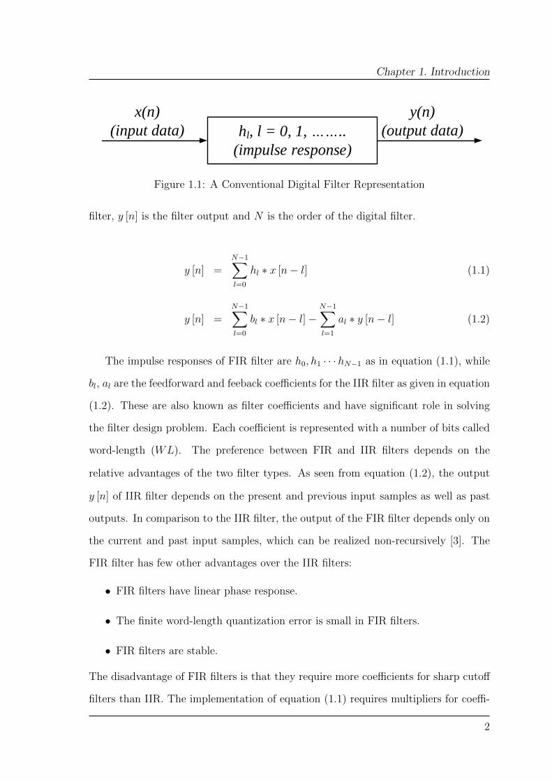
A digital filter is a system that uses discrete time signals as input and produces a
digitally filtered discrete time output signal as shown in Figure 1.1. The digital filter
characteristics depends on the impulse response of the system. The digital filters are
classified as infinite impulse response (IIR) and finite impulse response (FIR) filters
based on the impulse response duration. The FIR and IIR filter equations are given in
equation (1.1) and equation (1.2) respectively, where, x [n] is the input to the digital
1
Chapter 1. Introduction
hl, l = 0, 1, ……..
(impulse response)
x(n)
(input data)
y(n)
(output data)
Figure 1.1: A Conventional Digital Filter Representation
filter, y [n] is the filter output and N is the order of the digital filter.
y [n] =N−1∑l=0
hl ∗ x [n− l] (1.1)
y [n] =N−1∑l=0
bl ∗ x [n− l]−N−1∑l=1
al ∗ y [n− l] (1.2)
The impulse responses of FIR filter are h0, h1 · · ·hN−1 as in equation (1.1), while
bl, al are the feedforward and feeback coefficients for the IIR filter as given in equation
(1.2). These are also known as filter coefficients and have significant role in solving
the filter design problem. Each coefficient is represented with a number of bits called
word-length (WL). The preference between FIR and IIR filters depends on the
relative advantages of the two filter types. As seen from equation (1.2), the output
y [n] of IIR filter depends on the present and previous input samples as well as past
outputs. In comparison to the IIR filter, the output of the FIR filter depends only on
the current and past input samples, which can be realized non-recursively [3]. The
FIR filter has few other advantages over the IIR filters:
• FIR filters have linear phase response.
• The finite word-length quantization error is small in FIR filters.
• FIR filters are stable.
The disadvantage of FIR filters is that they require more coefficients for sharp cutoff
filters than IIR. The implementation of equation (1.1) requires multipliers for coeffi-
2

Chapter 1. Introduction
cient multiplication, adders for accumulation and memory devices for delays. Thus,
the higher-order FIR filter requires more computations and memory as compared to
IIR filter, if implemented for the same specifications. However, linear phase response
and stability are critical in many applications such as speech processing, digital audio
and video processing. Hence, FIR filters are preferred for these kind of applications.
The FIR filter implementations are further classified into fixed coefficient and pro-
grammable coefficient filters. In many applications such as hearing-aids, digital audio-
video encoders and mobile phones, non-varying filter specifications are required. The
filter coefficients for these specifications are generally calculated using conventional
methods before implementing the filter structure. Once calculated, the coefficients are
not changed during implementations of such filters. Hence, for a given specification,
the coefficients and its filter structure are fixed, and these implementations are known
as fixed coefficient FIR filters. However, some applications such as software defined
radio (SDR), DSP processors and filter banks require a filter structure with adaptive
coefficient sets. In these kind of implementations, the filter structure is independent
of coefficient set and hence, these are called as programmable FIR filters. The on-chip
implementation of these filter structures can be done using either application specific
integrated circuit (ASIC) or field programmable gate array (FPGA) methodology.
1.1 Motivation
In fixed and programmable filter implementations, equation (1.1) will be exploited,
and it can be observed that, FIR filtering is mere a sequence of multiplications and
additions with delay elements. The multipliers are required for coefficient multipli-
cation, which multiplies the discrete input x [n] with coefficients at every tap of the
filter. The adders are required for accumulation purpose, followed by the delay el-
ements for storing the accumulated result. The number of multipliers, adders and
delay elements depend on N while size of these elements depends on WL. Multipliers
3

Chapter 1. Introduction
consume most of the area and power in filter implementations. Therefore, improving
the multiplier performance will lead to an efficient filter implementation. In fixed
coefficient FIR filters, these multipliers are replaced with shift and add circuits de-
pending on the number of signed-power-of-two (SPT) terms present in a coefficient.
However, in programmable filters, dedicated hardware optimized multipliers are used
and these are dependent on WL rather than SPT terms. Hence, the major challenges
in implementing the FIR filter are summarized as follows:
• Efficient fixed coefficient filter design with suitable coefficient set that minimizes
the hardware.
• Programmable filter design utilizing efficient multipliers and adder using exist-
ing arithmetic techniques.
Several optimization techniques and algorithms have been presented in the past for
designing the fixed coefficient filters. Many of these algorithms have shown significant
improvements in the filter design. However, a number of optimization algorithms have
also evolved in recent years. Hence, there is a scope of improvement in filter design
using recently developed algorithms. Any method to improve the design and imple-
mentation of FIR filter is always welcome. Similarly, the various arithmetic circuits
have evolved in recent years and can be used for implementing the programmable as
well as fixed coefficient FIR filters. The main motivation of this thesis is to design
fixed coefficient FIR filters with suitable existing algorithms and to address the issues
related to faster arithmetic circuits used for implementing programmable filters.
1.2 Objectives and Contributions
In this thesis, some problems in design and implementations of fixed and programmable
coefficient FIR filters are addressed.
4

Chapter 1. Introduction
1.2.1 Objectives
The main objectives of the thesis are as follows:
• To propose a fixed coefficient FIR filter design with the minimum number of
SPT terms using optimization techniques. Coefficient multiplication is mostly
dependent on the number of SPT terms present in a coefficient. Hence, the
number of SPT terms may be minimized using existing optimization techniques
without compromising on the frequency response.
• Several signal processing applications use the residue number system (RNS) for
achieving higher clock frequency. However, the use of RNS doesn’t guarantee
an area and power efficient implementation. Hence, the main focus of this thesis
is to implement a hardware efficient fixed coefficient FIR filter using RNS.
• To propose an efficient programmable filter, which may be utilized in several
applications such as SDR and DSP processors. As most of these devices are
operated at higher clock frequencies, this thesis aims to design a high speed
programmable FIR filter.
1.2.2 Contributions
The main contributions of this thesis are:
• An approach for designing the fixed coefficient FIR filter using Differential Evo-
lution (DE) algorithm has been proposed. The main aim of this algorithm is to
obtain the filter coefficient set with the minimum number of SPT terms with-
out compromising on the frequency response of the filters. Later, the common
sub-expression elimination algorithm is used to minimize the number of adders.
The performance of the proposed filters is compared with those proposed in
recently published literature in terms of area, delay, power and power-delay
product (PDP ). One of the proposed filters was found to improve the PDP
5

Chapter 1. Introduction
gain by 29% compared to Remez algorithm. The proposed approach showed
improvements in filter design for the given specifications.
• An efficient fixed coefficient FIR filter structure can be implemented using a
well-known approach called distributed arithmetic (DA). In this approach, the
filter structure is independent of the number of SPT terms presented in a coef-
ficient. In DA approach, the inner product values of coefficients are stored in
a look-up table (LUT) and these values are accessed serially. In this method,
the throughput of the filter is less if input is taken serially. However, if input is
taken in parallel, then area of the filter is more. To balance both these terms a
decomposed LUT based FIR filter using the RNS is proposed. An efficient inner
product based RNS-FIR filter implementation has been proposed in this thesis.
The synthesis results have been compared with recently published RNS based
FIR filter. The proposed RNS-FIR filters show improvement in area, power and
delay gain.
• A high speed programmable FIR filter using efficient arithmetic circuits is pro-
posed in this thesis. Many of the programmable filters in the literature focus
on the coefficient multiplication. However, apart from the coefficient multipli-
cation, there exists an adder for accumulation, which also has the significant
role in the critical path delay. In this method, the final adder in multiplier and
accumulator are replaced with a 4:2 compressors. The compressors in place of
adders minimizes the critical path delay of the filter. The performance of the
proposed architectures are compared with recently published works and shows
better results in terms of delay and power-delay-product at the cost of more
area.
The fixed coefficient filters using DE algorithm and RNS-FIR filters are imple-
mented with gate-level Verilog HDL. These filters are synthesized in UMC 90nm
technology using Cadence RTL compiler. The programmable filters are also imple-
6

Chapter 1. Introduction
mented with gate-level Verilog HDL and these are synthesized using Altera Cyclone
II device using DSP builder.
1.3 Outline of the Thesis
The rest of this thesis is organized as follows:
1. Chapter 2 presents the methodology for designing the digital FIR filters. A
literature review on designing the fixed coefficient FIR filters with optimization
techniques is also presented in this chapter. The concept of DE algorithm
is further explained in detail in this chapter. The problem formulation for
obtaining the FIR filter coefficients using DE algorithm is also presented in this
chapter. The effectiveness of the DE algorithm for FIR filter is demonstrated
through an example. The filter implementations and their synthesis results
using DE algorithm are also discussed in this chapter.
2. Chapter 3 presents the background of RNS and its use in FIR filters. This is
followed by the concepts of DA approach, and its implementation in RNS based
FIR filter is discussed. The proposed RNS based FIR filters implementation,
and their synthesis results are also discussed in this chapter.
3. Chapter 4 discusses the various programmable filter architectures and their im-
plementations. The proposed high speed programmable FIR filter implementa-
tion and its synthesis results are also presented in this chapter.
4. Chapter 5 summarizes the contribution of this thesis and discusses the future
direction of work.
7

Chapter 2
FIR Filter Design using
Differential Evolution Algorithm
In many of the signal processing applications, the filter specifications may be fixed
and ideally a signal processing device must operate at higher clock frequencies with
low power consumption. However, in practice these are difficult to realize, thus, it
is important to design an efficient hardware (area, delay and power) for FIR filter.
An efficient hardware filter can be designed by computing a new set of coefficients by
optimizing the filter order (N) and it’s word-length (WL).
In this chapter, the existing techniques/algorithms for designing a fixed coefficient
FIR filter is presented. The main focus of this chapter is to investigate these algo-
rithms and then determine the suitable algorithm for designing the hardware efficient
FIR filter. This chapter is organized as follows: The procedure for designing the FIR
filter is discussed in section 2.1 followed by literature review of fixed coefficient FIR
filter in section 2.2. The basic algorithm of an efficient filter (obtained after literature
review) is described in section 2.3. A low-pass filter design and its simulation results
using the proposed algorithm obtained from the literature is described in section 2.4
followed by conclusions in section 2.5.
2.1 General Overview of FIR Filter Design
The design of FIR filter involves the following steps:
1. Specification of the filter requirements
8

Chapter 2. FIR Filter Design using Differential Evolution Algorithm
|H(ω)|
1 + δp
1 - δp
δs
ωp ωs 0 ω
Pass Band Stop BandTransition width
Figure 2.1: Characteristics of a Low-Pass Filter
2. Calculation of the filter coefficients
3. Implementation of the filter architecture
2.1.1 Specification of the filter requirements
Any filter design starts with specifying the filter characteristics and design require-
ments. The specification of the filter includes, pass band edge frequency (ωp), stop
band edge frequency (ωs), pass band ripple (δp) and stop band ripple (δs). Addition-
ally, other design requirements such as hardware efficient filter structure (delay, power
and area) may be required for designing the FIR filter. Based on these requirements
the filter coefficients can be calculated.
The filter characteristics of a low pass filter is shown in Figure 2.1. In the pass
band, the magnitude response has a peak deviation of δp where as δs is the maximum
deviation in the stop band. The magnitude response decreases from the pass band
to the stop band in the transition band region. The pass band and stop band ripple
values (δp and δs respectively) may be expressed in linear scale or in decibel (dB)
9

Chapter 2. FIR Filter Design using Differential Evolution Algorithm
scale. The minimum stop band attenuation (As), maximum pass band attenuation
(Ap1) and minimum pass band attenuation (Ap2) in (dB) are given below:
As = −20 log10 δs
Ap1 = 20 log10(1 + δp)
Ap2 = 20 log10(1− δp)
(2.1)
2.1.2 Calculation of the filter coefficients
A number of approaches has been proposed for finding the filter coefficients. The
window, frequency sampling and optimal algorithm are the most commonly used
methods for finding the filter coefficients [3]. The window method employs window
function which could have either a fixed or variable pass band/stop band ripple. The
most commonly used fixed window functions are Rectangular, Hanning, Hamming,
Blackman and Bartlett [4]. In fixed window functions, δp and δs values are fixed and
equal. Hence, the designer may end up with either too small a pass band ripple or
too large stop band attenuation [3,4]. In case of variable window such as Kaiser, the
δp and δs values are chosen with the help of the ripple control parameter set by the
designer [4].
Alternative approach is the frequency sampling in which the filter coefficients
are computed by sampling the ideal filter in the frequency domain. This approach
lacks precise control over the band edge frequencies or the passband ripples [5,6]. In
optimal approaches, the filter coefficients are obtained by minimizing the maximum
error between the desired and actual response using various optimization techniques
and are discussed in section 2.2. These approaches require more time to design the
filter as compared to the window and frequency sampling methods. However, the
optimal approaches are more popular as the resultant filter coefficients leads to an
hardware efficient FIR filter with filter’s desired frequency response [7, 8].
10
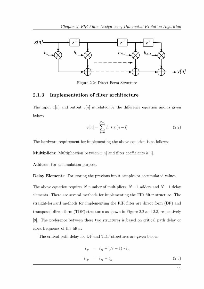
Chapter 2. FIR Filter Design using Differential Evolution Algorithm
y[n]
z-1x[n]
h0 h1
z-1
hN-2
z-1
hN-1
Figure 2.2: Direct Form Structure
2.1.3 Implementation of filter architecture
The input x[n] and output y[n] is related by the difference equation and is given
below:
y [n] =N−1∑l=0
hl ∗ x [n− l] (2.2)
The hardware requirement for implementing the above equation is as follows:
Multipliers: Multiplication between x[n] and filter coefficients h[n].
Adders: For accumulation purpose.
Delay Elements: For storing the previous input samples or accumulated values.
The above equation requires N number of multipliers, N − 1 adders and N − 1 delay
elements. There are several methods for implementing the FIR filter structure. The
straight-forward methods for implementing the FIR filter are direct form (DF) and
transposed direct form (TDF) structures as shown in Figure 2.2 and 2.3, respectively
[9]. The preference between these two structures is based on critical path delay or
clock frequency of the filter.
The critical path delay for DF and TDF structures are given below:
tdf
= tM
+ (N − 1) ∗ tA
ttdf
= tM
+ tA
(2.3)
11

Chapter 2. FIR Filter Design using Differential Evolution Algorithm
hN-1 hN-2 hN-3 h0
y[n]
x[n]
z-1z-1
z-1
Figure 2.3: Transposed Direct Form Structure
where, tdf
and ttdf
are the critical path delay of DF and TDF where as tM
and tA
are
the critical path delays of multiplier and adder, respectively.
From the Figure 2.2, it can be infer that tdf
consists of one multiplier and N − 1
adders where as in Figure 2.3, ttdf
consists of only one multiplier and one adder. Due
to this, TDF structures are faster and operates at higher clock frequencies and thus
this structure is chosen over DF structure for many filter applications [9].
2.2 Literature Review of Fixed Coefficient FIR Fil-
ter
In TDF structures, the multipliers require more power and area in the circuit when
compared with the adders. Thus, it is a common practice in fixed coefficient filters to
use a multiplier-less realization which could be achieved by replacing the multiplier
with shift and adder circuits. Hence, in multiplier-less realization, the filter coefficients
are represented either as sum or difference of SPT terms [10]. The SPT terms are
usually defined as {1, 0, 1}; 1 represents −1. The adder cost depends on the number of
SPT terms that are present in the filter coefficients and thus, minimizing the number
of SPT terms can reduce the complexity of FIR filter structure [10].
Lets take an example to describe the SPT term using the conventional and canon-
ical sign digit approaches.
12

Chapter 2. FIR Filter Design using Differential Evolution Algorithm
Example 2.2.1. In this example, a 4 bit coefficient multiplication using the conven-
tional and canonical sign digit approaches are described.
Conventional Approach
Consider a 4 bit coefficient h = 15d = 1111b. The coefficient multiplication with input
X is given below:
X × h = 15×Xd
= X × 23 +X × 22 +X × 21 +X × 20
= X << 3 +X << 2 +X << 1 +X (2.4)
For implementing the above equation 3 adders are required as shown in Figure 2.4(a).
Canonical sign digit (CSD) Approach
In Canonical Sign Digit (CSD), the coefficient h = 15d = 1111b is represented as
10001 [11]. The coefficient multiplication with input X is given below and it’s imple-
mentation is shown in Figure 2.4(b) .
X × h = 15×Xd = X × 24 −X × 20
= X << 4−X (2.5)
The CSD approach requires only 1 adder for coefficient multiplication as the num-
ber of SPT terms are reduced from 4 to 2. From the above two approaches, it clearly
shows that, the number of adders are minimized by reducing the SPT terms. Hence,
the main focus of many researchers is to find a coefficient set with the minimum
number of SPT terms without compromising on the frequency response. There are
number of algorithms in the literature for reducing the number of SPT terms. These
algorithms rely on the idea that the sets of filter coefficients are not unique for a given
filter specification [12].
13

Chapter 2. FIR Filter Design using Differential Evolution Algorithm
XX << 1X << 2X << 3
X × h(a) Linear Addition
-XX << 4
X × h(b) CSD Approach
Figure 2.4: Coefficient Multiplication with Adders
2.2.1 Literature Review
The filter coefficient calculations using optimal algorithms are widely used due to the
availability of programming techniques. The filters designed with these algorithms
offers desired frequency response and reduced number of SPT terms.The basic idea
of these algorithms is to minimize the error that is measured as difference between
the desired filter response and the response of the filter being designed. There are
many algorithms in the literature for the FIR filter design. However, a few of them
are addressed in this thesis, which are very well-known in the field of FIR filter
design [7, 8, 10,12–47].
Linear programming technique has been used for finding the filter coefficients [13].
The computation time required for linear programming is far greater than Remez
algorithm [14]. An algorithm by Parks and McClellan for optimal FIR filter design
using the Remez exchange algorithm [14]. A detailed description of how to program
the FIR filter is given in [8]. A general-purpose integer programming along with
branch and bounce algorithm by Kodek is used to design the optimal FIR filter [15].
Lim and Parker, presented a mixed integer linear programming (MILP) method for
14
Chapter 2. FIR Filter Design using Differential Evolution Algorithm
designing the FIR filter. The results obtained by Lim and Parker are compared with
simple rounding of coefficient values and show significant improvement in the desired
filter response [16].
A local search algorithm with powers-of-two coefficients by Zhao and Tadakoro [17]
improves the filter response and minimizes the error as compared to MILP given
in [16]. Samueli presented a two-stage local search algorithm for the design of mul-
tiplierless FIR filters [10]. The coefficients are represented as sums or differences of
powers-of-two known as CSD. An important property of CSD is, no two consecutive
bits in a CSD number are non-zero [11]. In CSD, one additional non-zero digit is
required as compared to the Binary Coded (BC) number. However, in [10], δs value
of the filter is approximately equal to the theoretical δs value. An efficient FIR im-
plementation of bit-serial and bit-parallel circuits based on CSD representation was
given in [18]. The algorithm by Li et al., presents a variable number of SPT terms for
each coefficient [20]. This algorithm is compared with MILP and shows improvement
in δs value. The multiplierless FIR filters are implemented in [23–25].
So far, in the literature, most of the algorithms are used for designing the FIR
filter with the desired response. Some algorithms such as [10, 23] discuss on FIR
filter complexity reduction. The number of SPT terms are reduced by 33% in CSD
representation and thus some reduction in the number of adders can be achieved
in FIR filter coefficient multiplication. However, a method by Hartley in [26], uses
common subexpressions with CSD, which results in decrease in the number of adders
by about 50%. This method often referred as common subexpression elimination
(CSE). A fast branch and bounce algorithm is proposed with reduced constraints
proposed by Cho and Lee in [30] improves the filters response as compared to the
conventional branch and bounce algorithm in [16]. Chen and Willson developed an
efficient two-stage algorithm in which the first stage contains a prototype algorithm
followed by the trellis search algorithm for minimizing the error between the desired
15

Chapter 2. FIR Filter Design using Differential Evolution Algorithm
filters response and obtained response [31]. Further, the number of adders are reduced
by subexpression sharing with the help of a merge-search algorithm. The number of
SPT terms in [31] are reduced as compared to the methods in [10, 16, 20] without
compromising on the desired filters response.
Lim et al., introduced the SPT term allocation for filter coefficient set in [32]. In
this approach, the number of SPT term allocated for each coefficient is determined
in first stage followed by optimizing the coefficient value using integer-programming
algorithm. The two-stage algorithm proposed by Kaakinen and Saramaki [33] further
reduces the SPT terms as compared with Lim and Chao and Willson [16, 31]. A
two-stage algorithm by Feng and Teo is presented in [35] consists of local search and
global search algorithm. This method also shows significant improvement in filters
response as compared to Li et al.,, Chen and Willson in [20,31]. Yao and Chien [34]
introduced a three-stage algorithm, first a prototype FIR filter was designed using
the Remez exchange algorithm and then the coefficients are scaled by a scaling factor
and are represented in CSD. In final stage, a partial MILP algorithm was applied to
the filter coefficients for reducing the number of SPT terms.
The algorithms proposed by [10,16,20,31,33,48] are useful for designing the FIR
filters without using the CSE. In [36], Xu et al., implements an algorithm for the FIR
filter design with reusable common subexpressions where common SPT terms are
scaled and rounded to obtain the CSD coefficients set in the first stage. In the second
stage, using the local search algorithm, the maximum peak ripple is optimized. Sub-
sequently the algorithm uses the most frequently used subexpressions for minimizing
the number of adders to implement FIR filters. The results of this algorithm show
significant reduction in area of the filter as are compared with [10,16,20,31,33]. Alter-
native design of FIR filter with subexpression in one stage using MILP algorithm was
given in [37]. Aktan et al., presents a modified branch and bounce algorithm named
as FIRGAM for minimizing the total number of SPT terms in a coefficient set [12].
16

Chapter 2. FIR Filter Design using Differential Evolution Algorithm
This algorithm also reduces the number of SPT terms presented in each coefficient,
which leads to an effective FIR filter implementation.
In [40], Yu et al., presented a method for reusing the CSE for FIR filter imple-
mentation. An algorithm by Shi and Yu [43], presents an FIR filter with a minimum
number of adders. Most of the methods proposed in the literature in general, are
considered for reduction in hardware cost. These methods are categorized into op-
timal and suboptimal approaches. Optimal approach employs mixed integer linear
programming, which requires a lot of computation time. On the other hand, although
suboptimal approach does not guarantee the optimal results, quasi optimal results
can be obtained in reasonable time using this approach [36].
Heuristic algorithms have a unique feature of search within its neighborhood to
obtain optimal solution. Hence, heuristic optimization algorithms, such as simulated
annealing and genetic algorithm (GA), are highly popular in digital filter design
[49–73]. Most of these methods are used to design FIR filter for the desired response.
However, as in optimal approaches discussed above there is a scope of optimizing
the SPT terms using heuristic algorithms. These are most widely used as global
optimization methods. However, genetic algorithms are weaker in determining a local
minimum in terms of convergence speed. To overcome these shortcomings of genetic
algorithms, DE algorithm is preferred in various applications. DE finds the true
global minimum of a model search space, regardless of the initial parameter values.
It also has a very high convergence speed and uses only a few control parameters. DE
is, especially, applicable in solving unconventional filter design problems. As most of
the filter design tasks can be explained as problems to meet some given constraints
or a tolerance level, DE is highly applicable in digital filter design [61, 62]. However,
in [62], DE algorithm was used to obtain the coefficient set which meets the magnitude
response.
The objective of this thesis is to find a coefficient set using DE along with the
CSE algorithm. While DE algorithm finds several coefficient sets, which satisfy the
17

Chapter 2. FIR Filter Design using Differential Evolution Algorithm
magnitude response with a decreased number of SPT terms, CSE algorithm finds a
coefficient set from the above with decreased adder cost. DE algorithm is a stochastic,
population-based optimization algorithm introduced by Storn and Price [74]. DE is a
powerful non-deterministic algorithm, which searches for a solution, by generating and
refining the search spaces continuously. In each iteration step, the results are tested
for their fitness to survive, and whether they can form a part of the solution. Each
set of solutions is said to form one generation. The algorithm searches from a search
space of random solutions and iteratively refines the search space. Next, it samples
out some solutions randomly, calculates a vector difference of them and finally applies
this to the present solution. Thus the present solution now gets mutated; however,
it may or may not be better than before. If it is found to yield a better output,
it is retained, or else it is discarded. The above sequence of steps is repeated for
a sufficiently large number of times. The major steps in a DE algorithm for FIR
filter design are initialization, evaluation, mutation, recombination, evaluation, and
selection [74]. Here, the objective of the iterations is to generate the coefficients
with a minimum number of SPT terms in them, so that number of multiplications is
reduced. The DE and implementation of FIR filter using DE algorithm are discussed
in section 2.3.
2.3 Proposed Approach for FIR Filter Design
Differential Evolution (DE) is an optimization algorithm to find the optimum solution
for a given problem by iteratively trying to improve the solution without sacrificing
the system quality requirement. DE optimizes a problem by generating a population
of random solutions and creates a new solution by combining the existing ones. It uses
simple formulas for generating new solutions and finds the fitness on the optimization
problem. The steps involved in DE algorithm are discussed in this section.
18

Chapter 2. FIR Filter Design using Differential Evolution Algorithm
2.3.1 Differential Evolution Algorithm
Like most of the evolution algorithms (e.g. genetic, simulated annealing), DE is a
population-based optimizer that samples the objective function at randomly chosen
multiple initial points. Preset parameter bounds define the domain from which the NP
vectors in the initial population are chosen. Here, NP is population size. Each vector
is indexed by a number from 0 to NP − 1. Like other population-based methods
[61], DE generates new points that are perturbations of existing points, but these
deviations are neither reflections nor samples from a predefined probability density
function. Instead, DE perturbs vectors with the scaled difference of two randomly
selected population vectors [60].
A general flow chart of DE algorithm is shown in Figure 2.5. The flowchart shows
the steps involved in DE algorithm for the generation of new population. The major
steps involved in DE are population structure, initialization, mutation, cross-over
and selection. The detailed explanations of these steps are given in the following
subsections.
2.3.1.1 Population Structure
DE maintains two population vectors Sx and Sm (see Figure 2.5), each vector contains
NP L- dimensional elements. Here, L is the number of parameters to be determined.
The current population, Sx is composed of vectors Xi,g which is initial population or
updated new population. Each Xi,g vector consists of xj,i,g elements with j varying
from 0 to L-1, where g represents the current generation. The population Sx,g can be
written in equation form as given below:
Sx,g = Xi,g where i = 0, 1, · · · , NP − 1 and g = 0, 1, · · · , gmax
Xi,g = xj,i,g where j = 0, 1, · · · , L− 1 (2.6)
19

Chapter 2. FIR Filter Design using Differential Evolution Algorithm
X0,g X1,g X2,g X3,g Xi-1,g Xi,g
f(X0,g) f(X1,g) f(X2,g) f(X3,g) f(Xi-1,g) f(Xi,g)
Population
Sx,g
M0,g M1,g M2,g M3,g Mi-1,g Mi,g
f(M0,g) f(M1,g) f(M2,g) f(M3,g) f(Mi-1,g) f(Mi,g)
Mutant
Population
Sm,g
Cross Over
Select Trail
Or
Target Vector
X0,g+1 X1,g+1 X2,g+1 X3,g+1 Xi-1,g+1 Xi,g+1
f(X0,g+1) f(X1,g+1) f(X2,g+1) f(X3,g+1) f(Xi-1,g+1) f(Xi,g+1)
New
Population
Sx,g+1
+ -
F
+ +
C0,g = Trail Vector
Xr1,g Xr2,g
X0,g
5) X0,g+1 = C0,g if f(M0,g) ≤ f(X0,g)
= X0,g otherwise
1) Choose Target Vector and Base Vector
2) Random choice of two Population Numbers Xr1,g and Xr2,g
3) Compute weighted difference vector
4) Add to a base vector
Figure 2.5: Flow Chart for DE
where, gmax represents the maximum number of iterations that can be done. The ini-
tialization of the population is randomly done; however, the values of each parameter
should be defined within a pre-specified range, defined by lower and upper bounds,
UL and UB, respectively. These bounds define each of the elements in a row. The
elements of these vectors are given by ULj and UBj. Hence, when a random number
is generated between 0 and 1, it is multiplied with (ULj − UBj) and then added to
20

Chapter 2. FIR Filter Design using Differential Evolution Algorithm
ULj to generate a random number between ULj and UBj. Following equation shows
this process:
Xj,i,0 = randj(0, 1).(UBj − ULj) + ULj (2.7)
For first iteration g = 0. The random number generator, randj(0, 1), returns a
uniformly distributed random number between 0 and 1. The subscript, j, indicates
that a new random value is generated for each element [55,60]. Once initialized, DE
mutates randomly chosen vectors to produce an intermediary population, Sm,g, of NP
mutant vectors, Mi,g:
Sm,g = Mi,g where i = 0, 1, · · · , NP − 1 and g = 0, 1, · · · , gmax
Mi,g = mj,i,g where j = 0, 1, · · · , N − 1 (2.8)
Each vector in the current population is then recombined with a mutant to produce
a trial population, Sc,g, of NP trial vectors, Ci,g:
Sc,g = Ci,g where i = 0, 1, · · · , NP − 1 and g = 0, 1, · · · , gmax
Ci,g = cj,i,g where j = 0, 1, · · · , L− 1 (2.9)
2.3.1.2 Mutation
This step is used to create the intermediary mutant population (Sm) consisting of
mutant elements. In differential mutation, difference between two randomly selected
elements from (Sx) are taken and then multiply by a pre-decided scale factor F (usu-
ally range between 0 and 1). Finally, the resultant is added with another randomly
selected element from Sx [55, 60].
Mi,g = X1,g + F.(X2,g −X3,g) (2.10)
2.3.1.3 Recombination or Cross Over
This step is used to create the trial vectors for Sc population. It complemented
the mutation step. Crossover basically mixes up the two populations based on the
21

Chapter 2. FIR Filter Design using Differential Evolution Algorithm
crossover probability (Cr). It is pre-defined by the user like F and decides which
of the two populations Sx or Sm supplies the trial vector. If the random number
generated in the range (0, 1) is less than Cr, then the mutant element is copied
otherwise the element from Sx is selected. In addition, the trial parameter with
randomly chosen index, randj, is taken from the mutant to ensure that the trial
vector does not duplicate Xi,g.
Cj,i,g = mj,i,g if randj(0, 1) ≤ Cr or j = jrand
= xi,j,g otherwise
(2.11)
2.3.1.4 Evaluation
The frequency response of the initial coefficient set is calculated before and after
recombination. If the filter response is improved by introducing the mutant solution
vector, then the mutant vector is replaced with the older vector. In each iteration, a
new candidate is considered for replacement by a predetermined order. When all the
elements are checked for replacement, the new modified set constituted one generation
of samples. The above steps are repeated for a large number of generations, until the
coefficient sets obtained, fell within an error margin level set by the user.
2.3.1.5 Selection
Selection is the last step of a particular iteration or generation. Firstly, the cost
values or the objective function values of the trial vector and the target vectors are
compared. Secondly, the next-generation target vector consisted of either of these
depending on which one had a lower value. Once, the new population is selected, the
complete process starts again [55,60].
Xi,g+1 = Ci,g if f(ci,g) ≤ f(xi,g)
= Xi,j,g otherwise
(2.12)
22

Chapter 2. FIR Filter Design using Differential Evolution Algorithm
2.3.2 DE algorithm for FIR filter
The flowchart for the proposed methodology is shown in Figure 2.6. Apart from the
given filter specifications, the DE parameters, maximum number of iterations (IMax),
weight factor (F ) in the range (0,1), optimum cost value (OCV ) and population size
of coefficient vectors (NP ) are specified in this method. The order of the filter N is
obtained using Kaiser’s order formula [75].
At the first iteration of the algorithm, the initial filter coefficient set are selected
using equation (2.7). For I < IMax, mutation and crossover are computed using equa-
tion (2.10) and equation (2.11); resulting in a new set of coefficient vectors generated.
For this new set of coefficients, scaling factor is calculated for each set. Scaling factor
(sf) is the ratio of 2B to the maximum valued coefficient. Here B is the word length
of the filter coefficient. The quantized filter coefficients can be obtained by multiply-
ing each set of coefficients with 2B and its respective sf . The number of SPT terms
are evaluated for each set of coefficients described in [11]. The total adder cost is
estimated after applying the CSE elimination algorithm in [76]. By comparing with
the ideal response of the filter with a new set of coefficient, objcost is evaluated using
equation (2.14) and compared with the OCV . The algorithm ran until the objcost
became less than OCV or the maximum number of iterations occurred. The FIR
filter optimization problem for finding the filter coefficients is described as follows:
minimize : E = δPR − δPD
subject to: 1− δP ≤ H(ω) ≤ 1 + δP for ω ε [0, ωP ]
− δS ≤ H(ω) ≤ δS for ω ε [ωS, π]
(2.13)
where, δPD is the difference between the ideal peak pass band and peak stop
band attenuation and δPR is the difference between the peak pass band and peak
stop band attenuation obtained in each iteration. The error function E defined in
23

Chapter 2. FIR Filter Design using Differential Evolution Algorithm
Start
Specify filter specs: N , B, ωP , ωS, δP , δS and DE parameters: F , IMax, NP , OCV
Initial Population
if I < IMax
CrossoverMutation
Filter Coefficient set obtained
Quantization of Coefficients
Conversion of coefficients to CSD
Common Subexpression Elimination
Adder Cost and objcost Estimation
if objcost < OCV
Terminate Algorithm
Yes
Yes
No
No
Figure 2.6: DE Flow Chart for FIR Filter
24

Chapter 2. FIR Filter Design using Differential Evolution Algorithm
equation (2.13) can be obtained in each iteration. The objcost is evaluated based as
given in equation (2.14).
objcost = objcost + η for E < 0
= objcost for E ≥ 0
(2.14)
Here, η is a real number. The objcost value should be 0 for the first iteration. By
using equation (2.13), E will be evaluated. If δPR satisfies the filter specifications,
the value of E will be either positive or zero, else the value of E is negative. The
objcost remains identical if E is positive or zero, else a small value η will be added to
objcost. This objcost is compared with OCV and terminates the algorithm if the value
reaches to OCV or less, else DE starts with new population and follows the identical
procedure. Once, algorithms terminate, DE finds the filter coefficients. In the next
section, the algorithm is explained through an example.
2.4 Design Illustration and Simulation Results
In this section, the proposed DE algorithm is illustrated with an example. The sym-
metric FIR filter is designed using DE algorithm in the transposed direct form. The
benchmark filter specifications are taken from literature [36, 41, 43]. The normalized
pass band and stop band edge frequencies are 0.3π and 0.5π respectively. The pass
band and stop band, both had equal ripple value of 0.00316. The δs value in dB is -50
dB. The filter is implemented for different word length and order. The specifications
of the filter are defined in the objective function as defined in equation (2.14).
As mentioned in the previous section, the major steps in a DE algorithm for FIR
filter design include initialization, mutation, recombination, evaluation, and selection.
Among all steps, only initialization and mutation for the FIR filter are discussed
in this section. Rest of the steps are performed as discussed in section 2.3. The
25

Chapter 2. FIR Filter Design using Differential Evolution Algorithm
comparisons are based on the best published ones [36,41,43]. The results are compared
in terms of SPT terms, area, power and delay.
2.4.1 Initialization and Population
An initial set of the filter coefficients is constructed using the following expression.
Fcoefficient = UL+ rand(1,N + 1
2). ∗ (UB − UL) (2.15)
where UL, UB are the lower and upper limits of the filter coefficients and are given
as [-1,1]. The population NP , is considered as ten times that of the number of filter
coefficients [77]. Hence, NP is given as.
NP = 10 ∗ Fcoefficient (2.16)
2.4.2 Mutation
The mutant factor ’F ’ would have a range from (0, 1). The significance of mutation
was explained in section 2.3. The F value is chosen in such a way that it mutates
the population vectors effectively and converges to a better solution. Since DE is
sensitive to F , selection of F required manipulations. Initially, the FIR filters are
implemented for different values of F . Three sets of population vectors were obtained
for each value of F varying from 0.1 to 1 with the number of iteration as I1 = 25, I2
= 50 and I3 = 100. Then for each F value, three frequency responses were obtained
and plotted (Figures 2.7, 2.8 and 2.9).
In Figure 2.7(a) the F value is chosen as 0.1, and the magnitude responses are
shown for I1, I2, I3. The stop band and pass band attenuation for the above filter
were approximately 50 dB and 0 dB, respectively. However, for any value of the I1, I2
and I3 the responses of the filter are not matching with the ideal filter characteristics.
This suggests that the F chosen here is unsuitable for filter implementation. Similar
26

Chapter 2. FIR Filter Design using Differential Evolution Algorithm
0 0.1 0.2 0.3 0.4 0.5 0.6 0.7 0.8 0.9−70
−60
−50
−40
−30
−20
−10
0
Normalized Frequency (×π rad/sample)
Mag
nitu
de (
dB)
I1=25I2=50I3=100Remez
(a) F = 0.1
0 0.1 0.2 0.3 0.4 0.5 0.6 0.7 0.8 0.9−70
−60
−50
−40
−30
−20
−10
0
Normalized Frequency (×π rad/sample)
Mag
nitu
de (
dB)
I1=25I2=50I3=100Remez
(b) F = 0.2
0 0.1 0.2 0.3 0.4 0.5 0.6 0.7 0.8 0.9−70
−60
−50
−40
−30
−20
−10
0
Normalized Frequency (×π rad/sample)
Mag
nitu
de (
dB)
I1=25I2=50I3=100Remez
(c) F = 0.3
Figure 2.7: Magnitude Responses of LPF for Mutant Factor ‘F = 0.1, 0.2, 0.3’
27

Chapter 2. FIR Filter Design using Differential Evolution Algorithm
0 0.1 0.2 0.3 0.4 0.5 0.6 0.7 0.8 0.9−70
−60
−50
−40
−30
−20
−10
0
Normalized Frequency (×π rad/sample)
Mag
nitu
de (
dB)
I1=25I2=50I3=100Remez
(a) F = 0.4
0 0.1 0.2 0.3 0.4 0.5 0.6 0.7 0.8 0.9
−70
−60
−50
−40
−30
−20
−10
0
Normalized Frequency (×π rad/sample)
Mag
nitu
de (
dB)
I1=25I2=50I3=100Remez
(b) F = 0.5
0 0.1 0.2 0.3 0.4 0.5 0.6 0.7 0.8 0.9
−70
−60
−50
−40
−30
−20
−10
0
Normalized Frequency (×π rad/sample)
Mag
nitu
de (
dB)
I1=25I2=50I3=100Remez
(c) F = 0.6
Figure 2.8: Magnitude Responses of LPF for Mutant Factor ‘F = 0.4, 0.5, 0.6’
28

Chapter 2. FIR Filter Design using Differential Evolution Algorithm
0 0.1 0.2 0.3 0.4 0.5 0.6 0.7 0.8 0.9
−70
−60
−50
−40
−30
−20
−10
0
Normalized Frequency (×π rad/sample)
Mag
nitu
de (
dB)
I1=25I2=50I3=100Remez
(a) F = 0.7
0 0.1 0.2 0.3 0.4 0.5 0.6 0.7 0.8 0.9
−70
−60
−50
−40
−30
−20
−10
0
Normalized Frequency (×π rad/sample)
Mag
nitu
de (
dB)
I1=25I2=50I3=100Remez
(b) F = 0.8
0 0.1 0.2 0.3 0.4 0.5 0.6 0.7 0.8 0.9
−70
−60
−50
−40
−30
−20
−10
0
Normalized Frequency (×π rad/sample)
Mag
nitu
de (
dB)
I1=25I2=50I3=100Remez
(c) F = 0.9
0 0.1 0.2 0.3 0.4 0.5 0.6 0.7 0.8 0.9−70
−60
−50
−40
−30
−20
−10
0
Normalized Frequency (×π rad/sample)
Mag
nitu
de (
dB)
I1=25I2=50I3=100Remez
(d) F = 1
Figure 2.9: Magnitude Responses of LPF for Mutant Factor ‘F = 0.7, 0.8, 0.9, 1’
29

Chapter 2. FIR Filter Design using Differential Evolution Algorithm
process is repeated for different values of F in step of 0.1 starting from 0.2 to 1 and
plots obtained in each case for I1, I2 and I3 are shown in Figures 2.7, 2.8 and 2.9.
Close examination of the magnitude response plots, F =0.6 and I3 = 100 approaching
best towards the ideal response. Hence, the value of F is chosen as 0.6 by comparing
responses for different values of F . Once the mutant factor was chosen, DE mutated
and recombined the population to produce NP population trail set of filter coefficients.
2.4.3 Design of FIR Filter using DE Algorithm
The transposed direct-form FIR filter is implemented based on the equation in (2.17).
Y (n) =N−1∑k=0
hk ∗X(n− k) (2.17)
where, X(n) represents the input to the filter, h0, h1, · · · , hN−1 represents filter co-
efficients of length N , and Y (n) represents the filter output. The transposed direct
form of filter implementation, shown in Figure 2.3 consists of multipliers, adders and
delay elements.
The adders in the FIR filter realization can be categorized into structural adders
(SA) and multiplier adders (MA). The SA is used to add the input signal X(n),
multiplied by filter coefficient, along with stored value in delay element. Hence, the
adder cost of SA became equal to order of the filter. The MA are used to obtain the
product value of the filter coefficients multiplied by input X(n), by the shift and add
approach. The number of adders in a multiplier used for coefficient multiplication is
dependent on the number of non-zero bits present in the filter coefficients. In brief, the
adder cost of MA depends on the number of SPT terms present in filter coefficients.
However, the number of delay elements in FIR filter cannot be reduced, thus, the
complexity of FIR filters is largely dependent on adders required to implement the
filter coefficients. In this study, the objective of the DE algorithm is to design an FIR
30

Chapter 2. FIR Filter Design using Differential Evolution Algorithm
Table 2.1: FIR filter Coefficients
Filters h0 h1 h2 h3 h4 h5 h6 h7 h8 h9 h10 h11 h12 h13 h14
Remez -2 -9 1 19 16 -23 -49 1 87 70 -96 -212 1 543 1024
Xu [36] -11 0 25 23 -32 -70 0 128 106 -140 -316 0 814 1536 –
Yu [41] -1 -4 0 9 8 -11 -24 0 44 36 -48 -108 0 277 523
Shi [43] -2 -8 0 17 16 -21 -46 0 84 68 -92 -205 0 527 994
DE1 -1 -4 0 8 8 -8 -20 0 36 28 -45 -96 0 243 458
DE2 -1 -2 0 4 4 -4 -10 0 18 14 -23 -48 0 122 230
DE3 0 6 6 -12 -26 0 49 40 -66 -142 0 372 704 — —
filter with reduced hardware complexity without compromising on the filter response.
Hence, the objective function of the DE algorithm should calculate the filter coefficient
set in such a way that it would have the minimum number of SPT terms, resulting in
reduction of the number of MA. The FIR filters designed using DE algorithm named
as DE1, DE2 and DE3 are compared with methods proposed in [36], [41], [43]. The
coefficients of DE1, DE2 and DE3 along with Remez, Xu [36], Yu [41] and Shi [43]
are listed in Table 2.1.
The properties of the designed filters are summarized in Table 2.2, where N is
the order of the FIR filter (i.e., number of taps), WL represents the word length of
the filter coefficients, Asb represents stop band attenuation (in dB), SPT is the total
number of SPT terms presented in a filter coefficient set. MA and SA are numbers
of multiplier adders and structural adders, respectively, required to implement filter
coefficient set. The number of MA are obtained after applying CSE elimination
following the method described in [76]. SA is calculated using non-zero coefficient
values presented in the filter coefficient set. TA is the total adder cost obtained by
adding MA and SA.
31

Chapter 2. FIR Filter Design using Differential Evolution Algorithm
Table 2.2: Properties of the designed filters
Filters N WL Asb(dB) SPT SPT gain(%) MA SA TA TA gain(%)
Remez 30 10 -50.13 66 10 30 40
Xu [36] 28 12 -50.05 62 6.06 8 22 30 25
Yu [41] 30 10 -51.74 56 15.151 6 23 29 27.5
Shi [43] 30 10 -51 60 9.09 6 23 29 27.5
DE1 30 9 -52.96 50 24.242 7 23 30 25
DE2 30 8 -51.74 46 30.303 7 23 30 25
DE3 26 10 -50.76 52 21.212 8 19 27 32.5
The magnitude response of DE1, DE2, DE3 filters and the other filters by Remez,
Xu [36], Yu [41] and Shi [43] are plotted in Figure 2.10. The magnitude responses
of DE1, DE2, and DE3 are plotted in Figure 2.11 for the filter coefficients obtained
using DE algorithm.
The coefficients for the Remez algorithm are obtained by Remez function in MAT-
LAB [78] with filter length N = 30. The magnitude response of Remez filter in Figure
2.10 shows that the Remez filter satisfies Asb = -50 dB attenuation with WL = 10.
The SPT terms of the quantized coefficients can be obtained using binary to CSD
method by Parhi [11]. The MA cost is estimated using the method described in [76].
Table 2.2 shows the total number of SPT terms, MA, SA, and TA. The SPT term
reduction can be achieved either by finding a new set of coefficients or by reducing
WL without compromising on the filter response. In this proposed work, the DE
algorithm generated various coefficient sets for which the filter responses are verified
for different WL. With N =30 and WL = 10, Remez filter satisfied -50 dB stop band
attenuation (see Figure 2.10). The DE1 filter is designed choosing N = 30 and WL
= 9. By using the DE parameter mutant factor ’F ’ and by generating population
NP using equation (2.16), DE evaluates the objective function in every iteration with
32

Chapter 2. FIR Filter Design using Differential Evolution Algorithm
00.
10.
20.
30.
40.
50.
60.
70.
80.
9
−70
−60
−50
−40
−30
−20
−100
Nor
mal
ized
Fre
quen
cy (
×π r
ad/s
ampl
e)
Magnitude (dB)
R
emez
Xu
Yu
Shi
DE
1D
E2
DE
3
Fig
ure
2.10
:R
esp
onse
sof
Rem
ez,
Xu,
Yu,
Shi,
DE
1,D
E2
and
DE
3
33

Chapter 2. FIR Filter Design using Differential Evolution Algorithm
00.
10.
20.
30.
40.
50.
60.
70.
80.
9
−70
−60
−50
−40
−30
−20
−100
Nor
mal
ized
Fre
quen
cy (
×π r
ad/s
ampl
e)
Magnitude (dB)
D
E1
DE
2D
E3
Fig
ure
2.11
:R
esp
onse
sfo
rD
E1,
DE
2an
dD
E3
34

Chapter 2. FIR Filter Design using Differential Evolution Algorithm
a new set of filter coefficients. The objective function checks the filter response and
evaluates the error function E as in equation (2.13). After all iterations, DE gave the
coefficient sets, satisfying the magnitude response. By using binary to CSD method,
the SPT terms are evaluated for each coefficient set. The objcost and adder cost esti-
mation are computed by applying CSE elimination. Finally, a filter coefficient set is
chosen, which contained a minimum number of both SPT terms and TA.
Figure 2.11, shows that DE1 filter achieves -50 dB Asb value as per the filter
specifications. Table 2.2 shows the number of SPT terms obtained for Remez and
DE1, and these values are 66 and 50, respectively. Hence, the proposed approach
achieved a gain of 24.42% in SPT terms as compared to Remez algorithm. The gain
in SPT terms and adder cost are compared with methods [36,41,43] as shown in Table
2.2. However, the TA gain is not much better than Xu [36], Yu [41] and Shi [43].
The filter named DE2 is designed by further reducing the WL to 8 while keeping N
constant. The DE2 filter response also achieved -50 dB Asb as shown in Figure 2.11.
The numbers of SPT terms (shown in Table 2.2), are reduced as compared to DE1
without compromising on the magnitude response. After CSE elimination, the adder
cost is estimated for DE2, and found to be same as DE1. The adder cost can be
reduced by optimizing the order of the filter N. Among MA and SA; the cost of SA
can be reduced either by having a zero coefficient value or by reducing N value. If
coefficient value is zero, the product value is also zero; hence, SA is not required to
add to the stored value in delay element. However, it is always impossible to have
more coefficient values to be zero, hence by reducing N; the SA reduction can be
achieved. In the proposed work, DE1 and DE2 are designed with N = 30; however,
DE3 is designed with N = 26 with WL = 10 for reducing the adder cost further. The
SPT gain for DE3 is 21.2% as compared to Remez (shown in Table 2.2); however, the
SPT gain is slightly reduced as compared to DE1 and DE2. The gain in TA is much
more improved as compared to DE1 and DE2 as well as Remez. It is observed that,
35
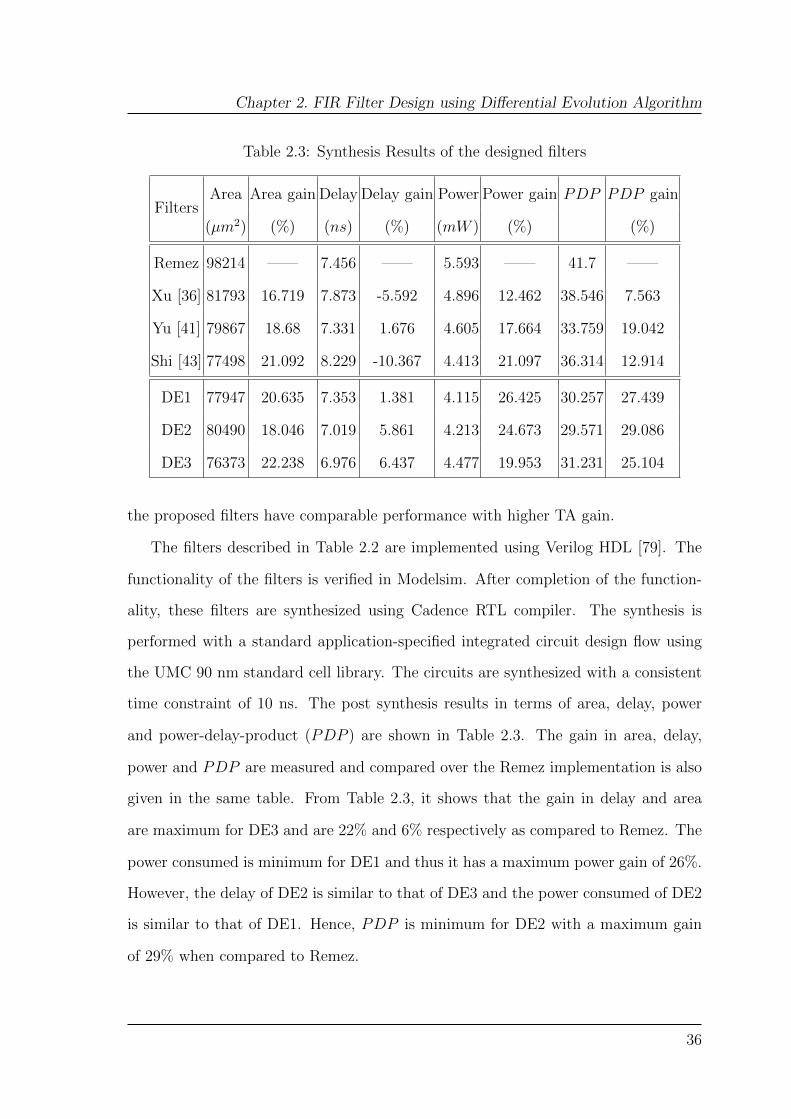
Chapter 2. FIR Filter Design using Differential Evolution Algorithm
Table 2.3: Synthesis Results of the designed filters
FiltersArea Area gain Delay Delay gain Power Power gain PDP PDP gain
(µm2) (%) (ns) (%) (mW ) (%) (%)
Remez 98214 —— 7.456 —— 5.593 —— 41.7 ——
Xu [36] 81793 16.719 7.873 -5.592 4.896 12.462 38.546 7.563
Yu [41] 79867 18.68 7.331 1.676 4.605 17.664 33.759 19.042
Shi [43] 77498 21.092 8.229 -10.367 4.413 21.097 36.314 12.914
DE1 77947 20.635 7.353 1.381 4.115 26.425 30.257 27.439
DE2 80490 18.046 7.019 5.861 4.213 24.673 29.571 29.086
DE3 76373 22.238 6.976 6.437 4.477 19.953 31.231 25.104
the proposed filters have comparable performance with higher TA gain.
The filters described in Table 2.2 are implemented using Verilog HDL [79]. The
functionality of the filters is verified in Modelsim. After completion of the function-
ality, these filters are synthesized using Cadence RTL compiler. The synthesis is
performed with a standard application-specified integrated circuit design flow using
the UMC 90 nm standard cell library. The circuits are synthesized with a consistent
time constraint of 10 ns. The post synthesis results in terms of area, delay, power
and power-delay-product (PDP ) are shown in Table 2.3. The gain in area, delay,
power and PDP are measured and compared over the Remez implementation is also
given in the same table. From Table 2.3, it shows that the gain in delay and area
are maximum for DE3 and are 22% and 6% respectively as compared to Remez. The
power consumed is minimum for DE1 and thus it has a maximum power gain of 26%.
However, the delay of DE2 is similar to that of DE3 and the power consumed of DE2
is similar to that of DE1. Hence, PDP is minimum for DE2 with a maximum gain
of 29% when compared to Remez.
36
Chapter 2. FIR Filter Design using Differential Evolution Algorithm
2.5 Conclusion
In this chapter, an approach for the design of FIR filter with reduced number of SPT
terms using the evolutionary algorithm is presented. The DE algorithm is used as
the evolutionary algorithm for optimizing the filter design. This proposed approach
evaluated the filter coefficient sets followed by CSE elimination and determined the
number of SPT terms and total adder cost. The experimental results of the proposed
approach showed better improvements in area, delay, and power gain in comparison
to recent reported design methods. One of the proposed filter DE2, showed maximum
PDP gain of 29% than those designed using Remez algorithm. The results of this
study may lead to more improvement in filter design, whose coefficients are fixed.
37

Chapter 3
RNS-Based Fixed Coefficient FIR
Filters
Residue number system (RNS) has been preferred in many digital signal processing
(DSP) systems for achieving higher clock frequency. The main advantage of RNS is
that a large number can be represented by a set of small numbers, which improves
the speed of arithmetic operations such as addition and multiplication. However,
the disadvantages of the RNS arithmetic system have been binary to RNS, RNS
to binary conversions and these conversions are computationally intensive and are
time consuming circuits. It is understood from literature that the RNS arithmetic
circuits are area and power consuming circuits. There has been a continuous search
for overcoming these difficulties.
In this chapter, the implementations of RNS-based fixed coefficient FIR filters are
discussed. This chapter is organized as follows: Introduction on RNS and basic RNS
arithmetic circuits are discussed in section 3.1. RNS based FIR filters are discussed
in section 3.2. The selection of the moduli set for designing the FIR filter is discussed
in section 3.3. In section 3.4, modular multiplication for the selected moduli set is
described. Section 3.5 describes the proposed filter architecture with an example. In
section 3.6, the implementation methodology for the proposed filter architectures and
their synthesis results are summarized. Functional verification of the implemented
filters using Altera DSP builder is also discussed in the same section, followed by the
conclusions in section 3.7.
38

Chapter 3. RNS-Based Fixed Coefficient FIR Filters
Forward Conversion
X Y
x3 x2 x1 y3 y2 y1
Reverse Conversion
z3 z2 z1
Z
Figure 3.1: A Typical RNS based Arithmetic System
3.1 Introduction on RNS
RNS is a technique of representing a binary number by a set of numbers {m1, m2,
m3..., mq} called moduli. Here, q is the size of moduli set [80]. These moduli values
are relatively prime to each other. Any number can be uniquely represented in the
given dynamic range [0,M − 1] using such moduli set. The maximum number M , for
a given moduli set is defined using equation (3.1).
M =
q∏i=1
mi (3.1)
Most widely studied moduli sets employ modulus (mi) as a power of two. Considering
the value of q = 3, the possible moduli sets can be {2k − 1, 2k, 2k + 1} and {2k −
1, 2k, 2k±1 − 1} [81–83]. However, there are several moduli sets, which have larger
than three modulus such as {2k − 1, 2k, 2k+1 ± 1, 2k + 1} [84], where k is an integer.
A typical RNS based arithmetic system with the moduli set {m1, m2, m3} is shown
39
Chapter 3. RNS-Based Fixed Coefficient FIR Filters
in Figure 3.1. The inputs to this system are X, Y and the output from this system is
Z, where Z = X � Y , here � denote arithmetic operations {+,−,×}. In Figure 3.1,
〈x1, x2, x3〉, 〈y1, y2, y3〉, and 〈z1, z2, z3〉 are the residues of binary coded (BC) numbers
X, Y and Z, with respect to the moduli set 〈m1,m2,m3〉. The residues are defined
as x1 = |X|m1, x2 = |X|m2
, x3 = |X|m3, y1 = |Y |m1
, y2 = |Y |m2, y3 = |Y |m3
, and
z1 = |Z|m1, z2 = |Z|m2
, z3 = |Z|m3. The above arithmetic operations are performed
in parallel for each modulus as shown below.
Z = X � Y =
z1 = |x1 � y1|m1
z2 = |x1 � y1|m2
z3 = |x1 � y1|m3
The typical RNS arithmetic system shown in Figure 3.1 consists of forward conversion,
arithmetic circuits and reverse conversion. These blocks are discussed in detail within
the following section 3.1.1.
3.1.1 Forward Conversion
The forward conversion circuit is used to find the residues of a BC number. This block
is typically used in RNS immediately after the BC input. The forward conversion for
a j bit BC input X with a well-known moduli set {2k − 1, 2k, 2k + 1} is discussed.
The residues of BC input X are defined as 〈x1, x2, x3〉. The dynamic range for the
above moduli set from equation (3.1) is[0, 23k − 2k − 1
]. The maximum number X
requires 3k bits as shown in equation (3.2). For finding the residues, first divide the
input X into three k bit blocks, B1, B2 and B3 [85, 86] as shown in equation (3.2).
X = x3k−1
x3k−2
. . . x2k︸ ︷︷ ︸
B3
x2k−1
. . . xk︸ ︷︷ ︸
B2
xk−1
. . . x0︸ ︷︷ ︸B1
= 22kB3 + 2kB2 +B1 (3.2)
40

Chapter 3. RNS-Based Fixed Coefficient FIR Filters
B1B2B3
2k-1
Modulo
Adder
x2
2k-1
Modulo
Adder
x1
2k+1
Modulo
Adder
2k+1
Modulo
Adder
x3
~B2+1
Figure 3.2: Forward Converter
The residues 〈x1, x2, x3〉 are obtained as given in equation (3.3).
x1 = |B1 +B2 +B3|2k−1
x2 = |B1|2k
x3 = |B1 −B2 +B3|2k+1
(3.3)
The following example 3.1.1 shows the conversion of input X into residues.
Example 3.1.1. Consider k = 3, the moduli set {2k − 1, 2k, 2k + 1} = {7, 8, 9}. For
the input X = 351d = 101011111b, the decimal values B3, B2, B1 are 5, 3 and 7
respectively. Substituting B1, B2 and B3 values in equation (3.3), the residues are
obtained as follows:
x1 = |7 + 3 + 5|7 = 1
x2 = |7|8 = 7
x3 = |7− 3 + 5|9 = 0
The forward converter circuit implemented using equation (3.3) is shown in Figure
3.2. The residue x2 is the direct value of B1. The residues x1 and x3 are calculated
with two-stage modulo adders. The modulo addition is discussed in the following
section 3.1.2.
41

Chapter 3. RNS-Based Fixed Coefficient FIR Filters
Adder
YX
S’
Adder
m~
2:1 Mux
S’-m
Cout
|X+Y|m
Figure 3.3: Basic Modulo Adder
3.1.2 Modulo Addition
The modulo-m addition of two numbers X and Y , where 0 ≤ {X, Y } < m is defined
in [87] which is given in equation (3.4).
|X + Y |m =
{X + Y if X + Y < m
X + Y −m otherwise(3.4)
The modulo adder (MA) using equation (3.4) can be implemented as shown in
Figure 3.3. First, it produces sum S ′ by adding X and Y . If S ′ falls within modulus
value m, then S ′ is selected, else m is subtracted from S ′ to fall within m value.
Hence, two adders and a 2:1 multiplexer is required for implementing MA. The 2k
modulo adder is same as BC adder with carry-out neglected. Hence, only 2k − 1 and
2k + 1 modulo adder circuits are discussed.
42

Chapter 3. RNS-Based Fixed Coefficient FIR Filters
Adder1
YX
S1
2:1 Multiplexer
Sum
Adder2
S2
Cin=0
Cout
P
Sel
k ORk
k1
11
1kkYX Cin=1
1kk
ANDk
Figure 3.4: 2k − 1 Modulo Adder
3.1.2.1 2k − 1 Modulo Addition
In 2k − 1 modulo addition, the resultant sum should be within the range 0 ≤ 2k − 2.
The design of 2k−1 MA is based on the following three cases given in equation (3.5).
|X + Y |2k+1 =
X + Y if 0 ≤ X + Y < 2k − 1
0 if X + Y = 2k − 1
X + Y −m 2k − 1 < X + Y ≤ 2k+1 − 4
(3.5)
Based on the three cases mentioned above, the 2k − 1 MA circuit can be imple-
mented as shown in Figure 3.4. In Figure 3.4, both X and Y are added with Cin as
‘0’ and ‘1’ at the same time. The resultant sums are denoted as S1 and S2. The
sum value S1 is correct for the first case given equation (3.5). For the second case, a
signal P is generated by bit-wise AND of k bit S1. If P = 1, the resultant sum S1
is equal to 2k − 1 and needs to be subtracted from 2k − 1. In third case, if Cout = 1,
which means that S1 exceeds 2k−1 and hence 2k−1 needs to be subtracted from S1.
In second or third case, subtraction is basically adding a ‘1’ to the least significant
43

Chapter 3. RNS-Based Fixed Coefficient FIR Filters
Adder1 Adder2 2:1 Multiplexer0 1 Sel 0
X 0 1 0 X 0 1 0 Sum S1Y 0 1 1 Y 0 1 1
0 1 0 0 1 1S1 1 0 1 S2 1 1 0P 0
Cin
Cin
Cout
Cout
Figure 3.5: 2k − 1 MA Example for Case 1
Adder1 Adder2 2:1 Multiplexer0 1 Sel 1
X 0 1 1 X 0 1 1 Sum S2Y 1 0 0 Y 1 0 0
0 0 0 1 1 1S1 1 1 1 S2 0 0 0P 1
Cin Cin
Cout
Cout
Figure 3.6: 2k − 1 MA Example for Case 2
bit (LSB) of the sum S1. This is same as adding X and Y with Cin = ‘1’ which is
S2. The 2:1 multiplexer selects the correct Sum value based on the Sel value. The
Sel value is obtained by bit-wise OR of P and Cout. The 2k − 1 MA is demonstrated
with following example 3.1.2 for the three cases mentioned above.
Example 3.1.2. Consider k = 3, and hence the modulus m = 23 − 1 = 7.
Case 1: Consider X = 2d = 010b and Y = 3d = 011b. The addition steps of these
two numbers are shown in Figure 3.5. The Cout and P signals of Adder1 are
‘0’ which results Sel signal of 2:1 multiplexer is ‘0’. Hence, the resultant Sum
from 2:1 multiplexer is S1 = 101b = 5d.
Case 2: Consider X = 3d = 011b and Y = 4d = 100b. The addition of these two
numbers are shown in Figure 3.6. The Cout and P signals of Adder1 are ‘0’ and
‘1’ which results Sel signal of 2:1 multiplexer is ‘1’. Hence, the resultant Sum
from 2:1 multiplexer is S2 = 000b = 0d.
Case 3: Consider X = 6d = 110b and Y = 6d = 110b. The additions of these two
numbers are shown in Figure 3.7. The Cout and P signals of Adder1 are ‘1’ and
44

Chapter 3. RNS-Based Fixed Coefficient FIR Filters
Adder1 Adder2 2:1 Multiplexer0 1 Sel 1
X 1 1 0 X 1 1 0 Sum S2Y 1 1 0 Y 1 1 0
1 1 0 1 1 0S1 1 0 0 S2 1 0 1P 0
Cin Cin
Cout
Cout
Figure 3.7: 2k − 1 MA Example for Case 3
‘0’ which results Sel signal of 2:1 multiplexer is ‘1’. Hence, the resultant Sum
from 2:1 multiplexer is S2 = 101b = 5d.
3.1.2.2 2k + 1 Modulo Addition
The 2k + 1 modulo addition is discussed in this section. In 2k − 1 modulus, the
sum of two numbers exceeds the modulus value, whenever there is a carry out signal.
However, in case of 2k + 1 modulus it is difficult to find out whether a sum exceeds
the modulus value or not. For k =3, the modulus 2k + 1 is 9. Consider two numbers
X and Y within this modulus are 6 = 0110b and 7 = 0111b respectively. The addition
of X and Y is 13 = 1101b without any carry-out, and this value exceeds modulus
value 9. Another difficulty is to obtain the residue value of 2k +1 with same modulus,
which is ‘0’Consider two numbers 6 = 0110b and 3 = 0011b, the addition is 9 = 1001b
for which the residue should be ‘0’ with respect to the modulus 9.
The 2k + 1 MA shown in Figure 3.8 is implemented based on the cases given in
equation (3.6) [87].
|X + Y |2k+1 =
A if A ≥ 0
2k + |A+ 1|2k if A = -1
|A+ 1|2k otherwise
(3.6)
In equation (3.6), A is defined as X + Y −m, where m is 2k + 1. Three different
cases are considered for 2k + 1 modulo addition as given in equation (3.6). In the
45

Chapter 3. RNS-Based Fixed Coefficient FIR Filters
S
Sum
(MSB-1 to LSB)
CSA
YX
C
Adder1~Cout
Adder2
S1
Sum
(MSB)
m~
C1
k1
k+1k+1
k
k+1k+1k+1
1
P 1k
OR
1
AND
Figure 3.8: 2k + 1 Mod Adder
first case, if the value of A is positive or zero, the same value is retained as sum
value. Second case is considered when sum of two numbers is equal to 2k. Third
case is considered for A value less than zero. In all three cases, first A has to be
calculated. Hence, a carry save adder (CSA) is used to add the three values X, Y
and m as shown in Figure 3.8, where m is the two’s complement of m. The outputs
of CSA are defined as S and C respectively. The S and C values are added with
Adder1, which produces sum S1, carry-out Cout and P . The P value is obtained by
bit-wise AND of S1 values. The most significant bit (MSB) of final sum Sum is P
value only. To obtain the remaining bits of Sum, Adder2 is used by adding S1 and
C1 values as shown in Figure 3.8. The value of C1 is equal to P | ∼ Cout (‘|’ bit-wise
OR operation), where ∼ Cout is the one’s complement of Cout. The three different
cases in equation (3.6) are demonstrated with the following example 3.1.3.
46

Chapter 3. RNS-Based Fixed Coefficient FIR Filters
CSA Adder1 Adder2mm 0 1 1 1 S 0 1 1 1 S1 1 1 1X 1 0 0 0 C 1 0 0 0 0Y 1 0 0 0 S1 0 1 1 1 1 1 1S 0 1 1 1 1C 1 0 0 0 P 0
C1=P | ~Cout
Sum(MSB-1 to LSB)
Cout
Figure 3.9: 2k + 1 MA Example for Case 1
CSA Adder1 Adder2mm 0 1 1 1 S 0 0 1 1 S1 1 1 1X 0 1 1 0 C 0 1 1 0 1Y 0 0 1 0 S1 1 1 1 1 0 0 0S 0 0 1 1 0C 0 1 1 0 P 1
C1=P | ~Cout
Sum(MSB-1 to LSB)
Cout
Figure 3.10: 2k + 1 MA Example for Case 2
Example 3.1.3. Consider k = 3, which results m = 2k + 1 = 9. The 2’s complement
of m is represented as m and this value in binary is 0111.
Case 1: In this case, the typical values of X and Y are considered for modulo addi-
tion. Consider X = 8d = 1000b, Y = 8d = 1000b and m = 0111b. The addition
of these two numbers are shown in Figure 3.9. In the first-stage, CSA produces
the output S and C as 0111 and 1000 respectively. In second stage S and C
values are added using Adder1 by left shifting the C value by one bit. This
results three outputs S1, Cout and P as 0111, ‘1’ and ‘0’ respectively. Here the
value of P itself is MSB of Sum. In third stage, Adder2 adds the S1 with C1.
Here, MSB is not considered for addition, and the carry-out from this adder
is always neglected. This results in Sum as 111. By appending P in MSB to
Sum, the final sum value is 0111b = 7. By referring to the first case in equation
(3.6), the value of A is obtained as A = 8+8−9 = 7 and the same are obtained
with adder circuit shown in Figure 3.8.
Case 2: In this case, consider the values of X and Y such that the sum of these
two numbers is equals to 2k. Consider X = 6d = 0110b, Y = 2d = 0010b and
m = 0111b. The addition of these two numbers are shown in Figure 3.10. In the
47

Chapter 3. RNS-Based Fixed Coefficient FIR Filters
CSA Adder1 Adder2mm 0 1 1 1 S 0 0 0 1 S1 1 0 1X 0 0 1 0 C 0 1 1 0 1Y 0 1 0 0 S1 1 1 0 1 1 1 0S 0 0 0 1 0C 0 1 1 0 P 0
C1=P | ~Cout
Sum(MSB-1 to LSB)
Cout
Figure 3.11: 2k + 1 MA Example for Case 3
first-stage, CSA produces the output S and C as 0011 and 0110 respectively.
The S1, Cout and P of Adder1 are obtained as 1111, 0 and 1 respectively. Hence,
the MSB of Sum is ‘1’The Sum from Adder2 is obtained as 000. By appending
P in MSB to Sum, the final sum value is 1000b = 8. By definition the value of
A is obtained as A = 6+2−9 = −1, which satisfies the second case in equation
(3.6). The sum will be obtained in such a case as 23 + |6 + 2 − 9 + 1|8 = 8
as given in equation (3.6), which is same as the sum obtained from the adder
circuit shown in Figure 3.8.
Case 3: In this case, consider X and Y as 2 = 0010b and 4 = 0100b respectively.
The value of A is obtained as 2 + 4 − 9 = -3, which satisfies the third case in
equation (3.6). In this case, the sum is obtained as | − 3 + 1|8 = 6. The same
adder circuit shown in Figure 3.8 is used for this case also and the values for
each stage are shown in Figure 3.11. The MSB of Sum is obtained as ‘0’ and
the remaining bits from Adder2 are obtained as 110, which result the final sum
as 0110b = 6.
In this section the design of 2k±1 modulo adders are discussed and demonstrated
with the examples. Another important arithmetic operation in RNS is modulo mul-
tiplication, which plays a significant role in FIR filter design and will be discussed in
next section 3.1.3.
3.1.3 Modulo Multiplication
Modular multiplication of RNS is essentially computing the product of two numbers
and then reducing it to the modulo value m. The basic modular multiplication of
48

Chapter 3. RNS-Based Fixed Coefficient FIR Filters
S
|X × Y|m
Modulo Partial
Product Generation
YX
C
Modulo CSA
Stages
Modulo Adder
Figure 3.12: Basic Modulo Multiplier
RNS is shown in Figure 3.12. As in the natural binary number system (BNS), in
RNS also first partial products have to be generated. However, in RNS the values of
these partial products should be in the range of modulo value m. In the next stage,
these partial products are added with the help of CSA and modulo adder. The 2k±1
modulo multiplications are discussed in the following sections.
3.1.3.1 2k − 1 Modulo Multiplication
The circuit for a k bit 2k−1 modulo multiplier is shown in Figure 3.13. The maximum
residue of 2k−1 is 2k−2, and it can be represented by using k bit binary value. Hence,
the multiplier size for these moduli is k bit. The steps in the modular multiplication
are as follows:
49

Chapter 3. RNS-Based Fixed Coefficient FIR Filters
S
|X × Y|
Modulo Partial
Product Generation
YX
C
Modulo CSA
Stages
2k-1
Modulo Adder
2k-1
k k
PP0,1PP0,2PP0,k-2PP0,k-1
kk
k
Figure 3.13: k Bit 2k − 1 Modulo Multiplier
• Generate partial products.
• Obtain sum S and carry C from CSA stages.
• Add S and C using 2k − 1 modulo adder.
The binary representation of X and Y are given as
X = xk−1x
k−2· · ·x1x0
Y = yk−1yk−2· · · y1y0 (3.7)
50

Chapter 3. RNS-Based Fixed Coefficient FIR Filters
The partial products PP0,i are generated for every Y bit value as given in equation
(3.8)
PP0,i =k−1∑i=0
X × yi
(3.8)
where, i is an integer varying from 0 to k − 1.
The multiplication of two numbers within the modulus 2k − 1 is given as
|X × Y |2k−1 =
∣∣∣∣∣k−1∑i=0
2iPP0,i
∣∣∣∣∣2k−1
= |2k−1PP0,k−1 + 2k−2PP0,k−2 · · · 22PP0,2
+ 21PP0,1 + 20PP0,0|2k−1 (3.9)
In equation (3.9), the partial products are scaled by the powers of 2. In such cases,
the values of partial products may exceed to the modulus value 2k − 1. Hence, these
values to be reduced to modulus value and then given to the CSA stages. The binary
representation of partial product can be defined as
PP0,i = PP0,i,k−1PP0,i,k−2 · · ·PP0,i,1PP0,i,0 (3.10)
The modulo power of 2 is defined as
2nPP0,i = PP0,i,k−n−1 · · ·PP0,i,0PP0,i,k−1 · · ·PP0,i,k−n (3.11)
where, n is an integer. Consider for k = 3, the PP0,i = PP0,i,2PP0,i,1PP0,i,0. Now
by using equation (3.11), the 22PP0,i is obtained as PP0,i,0PP0,i,2PP0,i,1. This shows
that 2n scaling for 2k − 1 modulus is simply left circular shifting the MSB values of
partial product and this shifting is simply the hardwired shift. These shifted partial
product values are given to CSA stages to obtain the S and C values as shown in
Figure 3.13. Finally, these two values are added using 2k − 1 modulo adder. Here, C
will be shifted by one bit as in equation (3.11).
51

Chapter 3. RNS-Based Fixed Coefficient FIR Filters
S
Modulo Partial
Product Generation
YX
C
Modulo CSA
Stages
k+1 k+1
PP0,1PP0,2PP0,k-2PP0,k-1
kk
2n
Correction
2
|X × Y|
2k+1Modulo Adder
2k+1
k+1
2:1 Multiplexer 2:1 Multiplexer
P’SP’c
Figure 3.14: k + 1 Bit 2k + 1 Modulo Multiplier
3.1.3.2 2k + 1 Modulo Multiplication
The 2k + 1 modulo multiplier is shown in Figure 3.14. The multiplier is designed
based in the following cases:
|X × Y |2k+1 =
∣∣Y + 2∣∣2k+1
if X = 2k∣∣X + 2∣∣2k+1
if Y = 2k
1 if X = 2k and Y = 2k
|X × Y |2k+1 otherwise
(3.12)
The above cases are implemented using the circuit shown in Figure 3.14 [88]. The
2k correction circuit is designed either by combinational circuit or using an LUT
52

Chapter 3. RNS-Based Fixed Coefficient FIR Filters
approach. The 2k correction unit is required to calculate the redundant product as
given in equation (3.13).
(P ′c, P′s) =
(Y , 1
)if X = 2k(
X, 1)
if Y = 2k
(0, 0) if X = 2k and Y = 2k
(3.13)
The partial products generated are similar as in 2k − 1 modulus. However, the 2n
scaling in these moduli is slightly different. The 2n scaling is defined as
2nPP0,i = PP0,i,k−n−1 · · ·PP0,i,0PP0,i,k−1 · · ·PP0,i,k−n (3.14)
The inverted MSB values are placed in LSB of partial products. The shifted partial
product values also exceeds the 2k + 1 modulus. Hence, a correction term is required
to get the correct value. And finally these values are added with 2k +1 modulo adder.
The arithmetic circuits (addition and multiplication) of 2k + 1 modulus involves
complex logic and requires more hardware as compared to 2k − 1 modulus. It can be
observed that the arithmetic computations of each modulus are totally independent.
Hence, if a large number is represented with a moduli set having a small value of k,
the arithmetic operations will be faster resulting higher clock frequency.
3.2 RNS Based fixed coefficient FIR Filters
Several techniques are proposed in literature for RNS-based FIR filter implementa-
tion [89–96]. All these filters were implemented using {2k − 1, 2k, 2k + 1} moduli set.
The 2k + 1 modulo multiplication and addition requires larger hardware as compared
to 2k − 1, 2k modulus. In [92, 93], the RNS-based FIR filters were implemented us-
ing distributed arithmetic (DA)approach. In [92], specific moduli set was used to
implement the RNS-DA based FIR filters. A low-power RNS-based FIR filter was
proposed by Wang et al. [93]. This method reduces the size of the reverse converter.
53
Chapter 3. RNS-Based Fixed Coefficient FIR Filters
The lookup table (LUT) partition technique was also presented by Wang, to reduce
the size of the memory. In DA-LUT approach, the inner product values are pre-
computed and are stored in RNS form. The required product values are accessed
serially from DA-LUT. These values are shifted and added in modular arithmetic to
obtain the complete output. The modulo shift addition involves complex logic cir-
cuits. The concepts of inner product computations and its use in DA based filters
were explained in [96–101]. The transfer function of an FIR filter is expressed as
Y =N−1∑l=0
hl ×Xl (3.15)
It is assumed that the filter coefficients hl are fixed values. The input with N
entries are represented as Xl = [XN−1 · · ·X1X0], each of j bit length. The input
entry Xl with binary weights can be expressed as follows:
Xl =
j−1∑n=0
bln × 2n bln ∈ [0, 1] (3.16)
where bln, is the nth bit of Xl which has binary value either 1 or 0. The 2n represents
the associated weight of the binary bits. By substituting equation (3.16) in equation
(3.15), the filter output Y can be written as
Y =N−1∑l=0
hl ×Xl
=N−1∑l=0
hl
j−1∑n=0
bln × 2n (3.17)
By interchanging the order of summations and bringing hl together with binary bits
of Xl
Y =
j−1∑n=0
{N−1∑l=0
hlbln
}2n (3.18)
54

Chapter 3. RNS-Based Fixed Coefficient FIR Filters
Let f (hlbln) =N−1∑l=0
hlbln (3.19)
Hence Y =
j−1∑n=0
f (hlbln) 2n (3.20)
The function in equation (3.19) contains the values representing the sum of products
with individual binary bit value bln of the input vector Xl. Since for the N number
of coefficients hl values are fixed and these are multiplied with bln, there are 2N
possible combination values based on equation (3.19). In DA approach, these values
are pre-computed and stored in an LUT. These values are accessed serially by giving
the present and past input bits as address to the LUT. The accessed pre-computed
values from LUT are first scaled with 2n, then added and stored in a register. The
FIR filter design with DA approach is demonstrated with example 3.2.1.
Example 3.2.1. Consider a 5th order FIR filter with j = 3 bit from [96]. The filter
equation with coefficients is shown below:
Y [n] = 3X[n] + 11X[n− 1] + 15X[n− 2] + 11X[n− 3] + 3X[n− 4] (3.21)
The coefficients are represented as hl = {h0, h1, h2, h3, h4} = {3, 11, 15, 11, 3}.
The 3 bit input vectors can be represented as follows:
X[n] = X0 = b02b01b00
X[n− 1] = X1 = b12b11b10
X[n− 2] = X2 = b22b21b20
X[n− 3] = X3 = b32b31b30
X[n− 4] = X4 = b42b41b40 (3.22)
55

Chapter 3. RNS-Based Fixed Coefficient FIR Filters
X(n)
DA
LUT
25
Entries
1
1X(n-4)
1X(n-3)
1X(n-2)
1X(n-1)
2n
ScalingAdder Register Y(n)
Scaling
Accumulator
Clock
Divider
Circuit
Clk
Acc_rst
Figure 3.15: FIR Filter Implementation using DA LUT
By substituting the above values in equation (3.18), the output Y [n] is obtained as
Y [n] =2∑
n=0
{3b0n + 11b1n + 15b2n + 11b3n + 3b4n} 2n
= {3b00 + 11b10 + 15b20 + 11b30 + 3b40} 20
+ {3b01 + 11b11 + 15b21 + 11b31 + 3b41} 21
+ {3b02 + 11b12 + 15b22 + 11b32 + 3b42} 22 (3.23)
From equation (3.19) and equation (3.20), it is evident that the size of DA LUT is
2N . In this example 3.2.1, the filter requires LUT size of 32 as N = 5. The 32 entries
to the LUT are based on the present and past input values. The LUT entries are
shown in Table 3.1. These values are computed based on the equation (3.19).
The FIR filter implementation using the DA LUT is shown in Figure 3.15. The
filter is designed with three basic building blocks. The first one is a DA LUT of size 25
= 32 as shown in Table 3.1. The second block is scaling accumulator, which consists
of 2n scaling, adder and a register and the third block is a clock divider circuit which
is required to reset the accumulator. The address to the LUT is the present input
56

Chapter 3. RNS-Based Fixed Coefficient FIR Filters
Table 3.1: DA LUT For N = 5
Address to LUT Entry Value
0 0 0 0 0 0 0
0 0 0 0 1 h4 3
0 0 0 1 0 h3 11
0 0 0 1 1 h4 + h3 14
0 0 1 0 0 h2 15
0 0 1 0 1 h2 + h4 18
0 0 1 1 0 h2 + h3 26
0 0 1 1 1 h2 + h3 + h4 29
0 1 0 0 0 h1 11
0 1 0 0 1 h1 + h4 14
0 1 0 1 0 h1 + h3 22
0 1 0 1 1 h1 + h3 + h4 25
0 1 1 0 0 h1 + h2 26
0 1 1 0 1 h1 + h2 + h4 29
0 1 1 1 0 h1 + h2 + h3 37
0 1 1 1 1 h1 + h2 + h3 + h4 40
1 0 0 0 0 h0 3
1 0 0 0 1 h0 + h4 6
1 0 0 1 0 h0 + h3 14
1 0 0 1 1 h0 + h4 + h3 17
1 0 1 0 0 h0 + h2 18
1 0 1 0 1 h0 + h2 + h4 21
1 0 1 1 0 h0 + h2 + h3 29
1 0 1 1 1 h0 + h2 + h3 + h4 32
1 1 0 0 0 h0 + h1 14
1 1 0 0 1 h0 + h1 + h4 17
1 1 0 1 0 h0 + h1 + h3 25
1 1 0 1 1 h0 + h1 + h3 + h4 28
1 1 1 0 0 h0 + h1 + h2 29
1 1 1 0 1 h0 + h1 + h2 + h4 32
1 1 1 1 0 h0 + h1 + h2 + h3 40
1 1 1 1 1 h0 + h1 + h2 + h3 + h4 43
57

Chapter 3. RNS-Based Fixed Coefficient FIR Filters
sample X(n) and previous input samples X(n−1), X(n−1), X(n−2), X(n−3) and
X(n− 4). The binary representation of a 3 bit input is given in equation (3.22). The
3 bit input samples considered are shown in Table 3.2. The binary representation of
X(n) is defined as bbn2bbn1bbn0
Table 3.2: Input Samples For FIR Filter
n Input X[n] bbn2 bbn1 bbn0
0 1 0 0 11 1 0 0 12 2 0 1 03 3 0 1 14 3 0 1 15 5 1 0 1
The inputs are taken serially in DA based filter implementations. One input
sample consists of 3 bits, hence the filter output is available for every three clock
cycles. The number of input samples and clock cycles are represented as n and tcycle
respectively. Initially, all the previous input samples are assumed to be ’0’. For some
n values the procedure for output is described in this example 3.2.1.
For n = 0: For tcycle = 0, the bb00 value ‘1’ is selected from Table 3.2. Hence, the
address to DA LUT is 10000, and from Table 3.1 the corresponding entry ‘3’
is selected and stored in a register. In the next clock, tcycle = 1, the bb01 is ’0’
which generates the address as 00000. The entry for this address is ’0’ and this
value is scaled by 2 and then added with previous value stored in the register.
Since the entry is ’0’, the adder output remains same as 3 and stored in the
register. The same process continues in the third clock cycle. Finally in the
third clock cycle, the filter output is obtained as 3 for n = 0 and tcycle = 2 as
shown in Table 3.3. The step by step execution of this FIR filter for every clock
cycle is shown in Table 3.3. The filter outputs are shown in bold-faced fonts.
The outputs are obtained for every three clock cycles for a 3 bit input sample.
58

Chapter 3. RNS-Based Fixed Coefficient FIR Filters
Table 3.3: Execution of DA FIR Filter
n tcycle X0 X1 X2 X3 X4 DA LUT Scaled Accumulator
00 1 0 0 0 0 3 31 0 0 0 0 0 0 3+0*2 = 32 0 0 0 0 0 0 3+0*4 = 3
10 1 1 0 0 0 14 141 0 0 0 0 0 0 14+0*2 = 142 0 0 0 0 0 0 14+0*4 = 14
20 0 1 1 0 0 26 261 1 0 0 0 0 3 26+3*2 = 322 0 0 0 0 0 0 32+0*4 = 32
30 1 0 1 1 0 29 291 1 1 0 0 0 14 29+14*2 = 572 0 0 0 0 0 0 57+0*4 = 57
40 1 1 0 1 1 28 281 1 1 1 0 0 29 28+29*2 = 862 0 0 0 0 0 0 86+0*4 = 86
50 1 1 1 0 1 32 321 0 1 1 1 0 37 32+37*2 = 1062 1 0 0 0 0 3 106+3*4 = 118
The clock divide circuit reset the accumulator for every three clock cycles. The
accumulator reset signal is represented as Acc rst as shown in Figure 3.15.
n = 1: In this case, the input samples are X0 = 001 and X1 = 001. The X1 value
is the input sample in n = 0 case. In every tcycle, the input bits are received
and the corresponding pre-computed values are selected from DA LUT. These
values are added as discussed in n = 0 case. The filter output in this case is
14. Again, the accumulator will be reset, and the present input sample will be
used in next case.
n = 2 to 5: For n = 2 to 5 the outputs of the filter will be obtained with the same
procedure discussed in n = 0 and 1 cases. For n = 4, the filter has all the
previous and present inputs X0, X1, X2, X3 and X4 as 3, 3, 2, 1 and 1. The filter
output for n = 4 and tcycle = 2 is obtained as 86 and is shown in Table 3.3.
This can be verified by substituting the filter coefficients and inputs in equation
(3.15).
59

Chapter 3. RNS-Based Fixed Coefficient FIR Filters
As the filter receives continuous input, this process remains same for all the input
samples. The throughput of this design is based on the size of the input j. In RNS,
as the large numbers are represented with small moduli sets, thus the throughput
of the system can be improved. Moreover, due to its small size modulo arithmetic
operations, the RNS offers higher clock frequency. Applying RNS to DA approach
with moduli set {2k − 1, 2k, 2k + 1} defined as M1, the filter output is given as
|Y |M1 =
∣∣∣∣∣j−1∑n=0
f(hlbln)2n
∣∣∣∣∣M1
=
∣∣∣∣∣j−1∑n=0
|f(hlbln)|M1 |2n|M1
∣∣∣∣∣M1
(3.24)
Let fM1
(hlbln) =
∣∣∣∣∣N−1∑l=0
hlbln
∣∣∣∣∣M1
(3.25)
The filter moduli output is rewritten as
|Y |M1 =
∣∣∣∣∣j−1∑n=0
fM1
(hlbln) |2n|M1
∣∣∣∣∣M1
(3.26)
In equation (3.26), the values of fM1
(hlbln) are pre-computed and stored in DA
LUT for each modulus. These values are accessed serially from LUT with the address
as present and previous input samples. However, first it is necessary to convert the
BC input to RNS using a forward converter. DA RNS-based FIR filters are proposed
by various researchers in the past [92,96,102–104]. The standard RNS DA based FIR
filter for each modulus with N = 5 is shown in Figure 3.16. In-spite of the advantages
in RNS, very few works have been reported in DA RNS filter. The major issue in RNS
DA based FIR filter is modulo scaling as given in equation (3.26) which is shown in
Figure 3.16. The modulo 2n scaling for 2k − 1 modulus can be implemented as given
in equation (3.11). However, as described in equation (3.14) the modulo scaling is
difficult to implement with 2k + 1 modulus. In [92] and [104], appropriate filters are
60

Chapter 3. RNS-Based Fixed Coefficient FIR Filters
Forw
ard
Co
nvert
erX
(n)
x 1(n
)
DA
LU
T
25
Entr
ies
1 1x 1
(n-4
)
1x 1
(n-3
)
1x 1
(n-2
)
1x 1
(n-1
)
Modulo
2n
Sca
ling
m1
Modulo
Adder
Regis
ter
Clo
ck
Div
ider
Cir
cuit
for
m1
Clk
Acc
_rs
t
x 2(n
)
DA
LU
T
25
Entr
ies
1 1x 2
(n-4
)
1x 2
(n-3
)
1x 2
(n-2
)
1x 2
(n-1
)
Modulo
2n
Sca
ling
m2
Modulo
Adder
Regis
ter
Modu
lo-m
2 S
cali
ng A
ccum
ula
tor
Clo
ck
Div
ider
Cir
cuit
for
m2
Clk
Acc
_rs
t
Modulo
-m1 S
cali
ng A
ccum
ula
tor
|Y(n
)|m
1
|Y(n
)|m
2
Rever
se
Con
vert
er
x 3(n
)
DA
LU
T
25
Entr
ies
1 1x 3
(n-4
)
1x 3
(n-3
)
1x 3
(n-2
)
1x 3
(n-1
)
Mo
dulo
2n
Sca
ling
m3
Modulo
Adder
Regis
ter
Modu
lo-m
3 S
cali
ng A
ccu
mula
tor
Clo
ck
Div
ider
Cir
cuit
for
m3
Clk
Acc
_rs
t
|Y(n
)|m
3
Y(n
)
Fig
ure
3.16
:D
AR
NS
Filte
rfo
rN
=5
61

Chapter 3. RNS-Based Fixed Coefficient FIR Filters
Y(n)Forward
ConversionX(n) TC
Conversion
DA
LUT
1
1
1
(BC)
Previous Input
samples in TC format
OHR
Modulo
Adder
Register
OHR to
RNS
conversion
Reverse
Conversion
tL-1
tL-2
t0
BC to TC Conversion Accumulator OHR to BC Conversion
Figure 3.17: DA RNS FIR Filter
designed for specific moduli set. In [102] a new modular approach with DA principles
was proposed by Lim and Premkumar.
Recently, a new RNS based DA approach for inner product computation was
proposed by Chan and Premkumar in [96]. The modulo 2n scaling issue is well
addressed in [96]. The FIR filter implementation using this RNS DA based inner
product computation is shown in Figure 3.17. The design in Figure 3.17 shows the
filter implementation for one modulus. This design uses thermometer code (TC)
representation for inputs, and one-hot coding (OHC) for modulo addition. The reason
behind the TC representation is due to the availability of RNS encoding based folding
analog-to-digital converter (ADC), which was designed by the same authors [105].
This ADC, converts the analog signal to thermometer code residue (TCR). Hence,
the forward conversion and residue to TC conversion are avoided. However, only
in few cases such as pre-processing filtering, the FIR filter receives the input signal
directly from ADC. Where as in other cases, the filter is used as an intermediate
block, then the input is received from the near by processing units.
In summary, the design in [96] requires forward and TC conversion circuits when
the input signal is not received directly from ADC. The filter shown in Figure 3.17 is
designed with binary code (BC) to TC conversion, accumulator and one-hot residue
(OHR) to BC conversion. The TC refers to the encoding format where the value is
62

Chapter 3. RNS-Based Fixed Coefficient FIR Filters
Table 3.4: Input Samples for RNS DA FIR Filter
n for x1tn Input values x1 = |X[n]|5 x1t
0 1 1 00011 1 1 00012 2 2 00113 3 3 01114 3 4 01115 5 0 0000
represented with a number of binary ‘1’ bits. For instance, decimal value 4 is encoded
in TC with a dynamic range of 6 as 001111. The decimal zero is encoded as 000000.
The TC encoding is not useful for larger dynamic range. However, TC encoding is
feasible in RNS as the large number is represented with small moduli set. The other
encoding used in [96] is OHC. In OHC, only one 1 bit is asserted for any number. For
instance, decimal value 4 is encoded in OHC with the dynamic range of 6 as 0010000.
The decimal zero is encoded as 0000001. When OHC is used to represent residues, it
is named as one-hot residue (OHR). Only one modulus filter design is demonstrated
with example 3.2.2.
Example 3.2.2. Consider the moduli set{
2k−1 + 1, 2k, 2k − 1}
, which is taken from
[96]. For demonstration, 2k−1+1 modulus is considered in this example as it is similar
to 2k + 1 modulus. For k = 3, the modulus is 5. The residues with this modulus are
represented as x1 . The residues of input samples X(n) and its TC encoding values
are shown in Table 3.4. The TC encoded x1 values are represented as x1t.
The size of the LUT in RNS DA filter is also dependent on N value. Hence, 25
pre-computed residues are stored in DA LUT as shown in Table 3.5. The address to
this LUT is present and past input sample residues, represented as x1tn. The x1tn
values are TC encoded as shown in Table 3.4. Initially, the previous input samples
are kept as 0. For n = 0 and tcycle = 0, the first input sample is LSB of 0001, which
is 1. Thus, the address to the LUT is 10000, for which the pre-computed value is 3.
The binary output of DA LUT is represented as b[0]b[1]b[2] as shown in Table 3.6.
These are the select signals for OHR modulo adder. Initially, the accumulator is reset
63

Chapter 3. RNS-Based Fixed Coefficient FIR Filters
2:1
Mux0
1
2:1
Mux0
1
2:1
Mux0
1
2:1
Mux0
1
2:1
Mux0
1
b[0]
a[0]
a[1]
a[2]
a[3]
a[4]
2:1
Mux0
1
2:1
Mux0
1
2:1
Mux0
1
2:1
Mux0
1
2:1
Mux0
1
b[1]
2:1
Mux0
1
2:1
Mux0
1
2:1
Mux0
1
2:1
Mux0
1
2:1
Mux0
1
b[2]
OHR[4]
OHR[3]
OHR[2]
OHR[1]
OHR[0]
Figure 3.18: OHR Modulo adder for modulus 5
to 0, hence; at first, input to the OHR adder is 000001 = 0d for mod-5. The OHR
modulo adder is shown in Figure 3.18.
The OHR adder shown in Figure 3.18 is designed based on 2:1 multiplexer. Hence,
it has two inputs. One is previous accumulated sum, represented as a[k]. Here k is an
integer varying from 0 · · · 2k−1. The second input (select signal) to the 2:1 multiplexer
is the output of DA LUT. The select signal is of k bit. The 2:1 multiplexer stages
in OHR adder are dependent on the size of DA LUT output and TC input samples.
In example 3.2.2, for k = 3, the size of DA LUT output and input sample is 3 bits
and 4 bits respectively. Hence, the OHR adder requires three stages with four 2:1
multiplexers in each stage. For n = 0 and tcycle = 0, the accumulator input is 00001
and select signal to multiplexer stages is b[0]b[1]b[2] = 011. Now the input of the OHR
adder shifted according to the select signal and gives the output as 01000, which is
shown in Table 3.6. The steps of accumulation addition is shown in Table 3.6. The
64
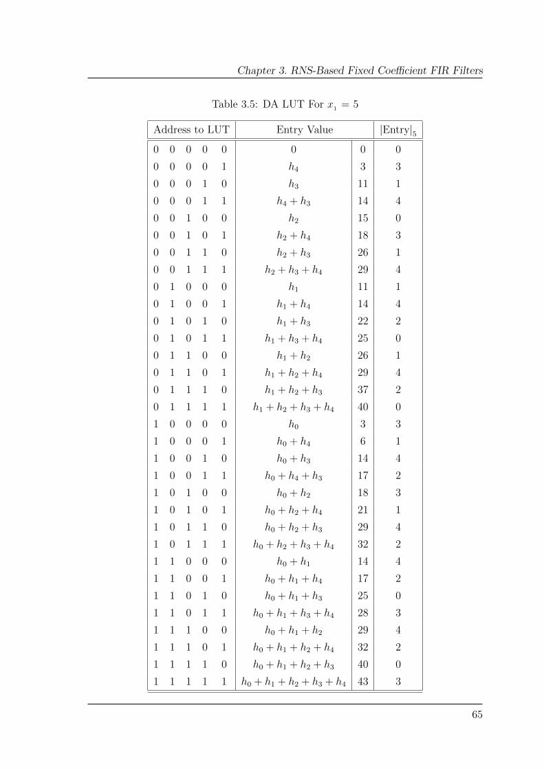
Chapter 3. RNS-Based Fixed Coefficient FIR Filters
Table 3.5: DA LUT For x1 = 5
Address to LUT Entry Value |Entry|50 0 0 0 0 0 0 0
0 0 0 0 1 h4 3 3
0 0 0 1 0 h3 11 1
0 0 0 1 1 h4 + h3 14 4
0 0 1 0 0 h2 15 0
0 0 1 0 1 h2 + h4 18 3
0 0 1 1 0 h2 + h3 26 1
0 0 1 1 1 h2 + h3 + h4 29 4
0 1 0 0 0 h1 11 1
0 1 0 0 1 h1 + h4 14 4
0 1 0 1 0 h1 + h3 22 2
0 1 0 1 1 h1 + h3 + h4 25 0
0 1 1 0 0 h1 + h2 26 1
0 1 1 0 1 h1 + h2 + h4 29 4
0 1 1 1 0 h1 + h2 + h3 37 2
0 1 1 1 1 h1 + h2 + h3 + h4 40 0
1 0 0 0 0 h0 3 3
1 0 0 0 1 h0 + h4 6 1
1 0 0 1 0 h0 + h3 14 4
1 0 0 1 1 h0 + h4 + h3 17 2
1 0 1 0 0 h0 + h2 18 3
1 0 1 0 1 h0 + h2 + h4 21 1
1 0 1 1 0 h0 + h2 + h3 29 4
1 0 1 1 1 h0 + h2 + h3 + h4 32 2
1 1 0 0 0 h0 + h1 14 4
1 1 0 0 1 h0 + h1 + h4 17 2
1 1 0 1 0 h0 + h1 + h3 25 0
1 1 0 1 1 h0 + h1 + h3 + h4 28 3
1 1 1 0 0 h0 + h1 + h2 29 4
1 1 1 0 1 h0 + h1 + h2 + h4 32 2
1 1 1 1 0 h0 + h1 + h2 + h3 40 0
1 1 1 1 1 h0 + h1 + h2 + h3 + h4 43 3
65

Chapter 3. RNS-Based Fixed Coefficient FIR Filters
Table 3.6: Execution of RNS DA FIR Filter
Inputs in TC RNS DA LUT OHR Adder
n tcycle x1t0 x1t1 x1t2 x1t3 x1t4 x1t5 Decimal b[0] b[1] b[2] Decimal OHR
0
0 1 0 0 0 0 0 3 0 1 1 3 01000
1 0 0 0 0 0 0 0 0 0 0 3 01000
2 0 0 0 0 0 0 0 0 0 0 3 01000
3 0 0 0 0 0 0 0 0 0 0 3 01000
1
0 1 1 0 0 0 0 4 1 0 0 4 10000
1 0 0 0 0 0 0 0 0 0 0 4 10000
2 0 0 0 0 0 0 0 0 0 0 4 10000
3 0 0 0 0 0 0 0 0 0 0 4 10000
2
0 1 1 1 0 0 0 4 1 0 0 4 10000
1 1 0 0 0 0 0 3 0 1 1 |4 + 3|5 = 2 00100
2 0 0 0 0 0 0 0 0 0 0 2 00100
3 0 0 0 0 0 0 0 0 0 0 2 00100
3
0 1 1 1 1 0 0 0 0 0 0 0 00000
1 1 1 0 0 0 0 4 1 0 0 4 10000
2 1 0 0 0 0 0 3 0 1 1 |4 + 3|5 = 2 00100
3 0 0 0 0 0 0 0 0 0 0 2 00100
4
0 1 1 1 1 1 0 3 0 1 1 3 01000
1 1 1 1 0 0 0 4 1 0 0 |3 + 4|5 = 2 00100
2 1 1 0 0 0 0 4 1 0 0 |2 + 4|5 = 1 00010
3 0 0 0 0 0 0 0 0 0 0 1 00010
5
0 0 1 1 1 1 1 0 0 0 0 0 00000
1 0 1 1 1 0 0 2 0 1 0 2 00100
2 0 1 1 0 0 0 1 0 0 1 |2 + 1|5 = 3 01000
3 0 0 0 0 0 0 0 0 0 0 3 01000
66

Chapter 3. RNS-Based Fixed Coefficient FIR Filters
outputs of the filter for every n input sample are shown in bold-faced fonts. The main
advantage of this modulo adder is modulo 2n scaling is overcome with TC and OHR
representations.
For k = 3, the moduli set is {5, 7, 8} and the highest modulus is 8. The filter output
for n = 0 is obtained after 4 tcycle for modulus 5, which is equal to 2k. Similarly, for
modulus 7 and 8 the throughput will be 6 and 7 respectively. Hence, the throughput
of the filter proposed in [96] is dependent on the maximum modulus presented in
the moduli set. The major issues in this design are the representation of residues for
higher modulus in TC, BC to TC conversion, OHR to BC conversion and RNS DA
LUT size, which depends on N . Hence, for simple modulo 2n scaling, a proper moduli
set is required for an efficient filter implementation. The main aim of this chapter is
to design filter with the following objectives:
• Modulo power of 2 scaling with appropriate moduli set selection.
• Eliminating the forward conversion circuit to improve the filter clock frequency.
• LUT based multipliers for improving the filter throughput.
First, the moduli set selection is discussed in section 3.3.
3.3 Selection of the Moduli Set
Modulo power of 2 scaling (2n) is encountered in RNS-based inner-product compu-
tation using the multiplier-less approach such as DA and LUT multipliers. Scaling a
number with 2n is not a problem in BNS, but modulo 2n scaling (|2n|mi) is difficult
to implement in hardware as the modulus operation of 2n with respect to mi involves
complex logic circuit [88]. The modulo 2n scaling is analyzed on an integer using
different moduli sets and observed that modulo 2n scaling can be implemented in
hardware similar to 2n scaling using bit-shifting, provided an appropriate moduli set
must be chosen.
67

Chapter 3. RNS-Based Fixed Coefficient FIR Filters
Table 3.7: Modulo 2n Scaling
Steps {2k − 1, 2k, 2k + 1} {2k − 1, 2k, 2k+1 − 1}
Moduli set (k = 3) {7, 8, 9} {7, 8, 15}
Digit size {3, 3, 4} {3, 3, 4}
DR 504 840
10 in RNS {3, 2, 1} {3, 2, 10}
Residue in binary {011, 010, 0001} {011, 010, 1010}
(10× 24) in RNS {|160|7, |160|8, |160|9} {|160|7, |160|8, |160|15}
Residue in binary {110, 000, 0111} {110, 000, 1010}
2k − 1 modulus 011→ 110 011→ 110
Bit-operation circular-shift circular-shift
2k modulus 010→ 000 010→ 000
Bit-operation linear-shift and linear-shift and
retaining k LSBs retaining k LSBs
2k + 1/2k+1 − 1 modulus 0001→ 0111 1010→ 1010
Bit-operation Circular-shift with (Only 4 left circular-shifts)
with correction
Suppose, an integer X = 10 to be scaled by 24 in RNS using two moduli set
{2k−1, 2k, 2k +1} and {2k−1, 2k, 2k+1−1} defined as M1 and M2 respectively. Step
by step, operations of modulo 2n scaling using moduli sets M1 and M2 are shown
in Table 3.7. For k = 3, the moduli sets M1 and M2 are {7, 8, 9} and {7, 8, 15}
respectively. The digit size in Table 3.7, is defined as the number of bits required to
represent, and it is {k, k, k + 1} bits for both M1 and M2 moduli sets. Hence, for
k = 3 the digit size is {3, 3, 4}. The DR for M1 and M2 is 504 and 840, which can
be obtained using (3.1).
Consider an integer X = 10, represented in RNS using the moduli sets M1 and
M2 as {3, 2, 1} and {3, 2, 10} shown in Table 3.7. The binary representation of the
68

Chapter 3. RNS-Based Fixed Coefficient FIR Filters
residues 〈x1, x2, x3〉 for the moduli set M2 is as follows:
x1 = {bk−1,1bk−2,1 · · · , b2,1b1,1b0,1}
x2 = {bk−1,2bk−2,2 · · · b2,2b1,2b0,2}
x3 = {bk,3bk−1,3 · · · b2,3b1,3b0,3}
(3.27)
The multiplications of a binary number X by 2n can be achieved by a simple left shift
operation by n bits. Similarly, multiplication of RNS number 〈x1, x2, x3〉 with 2n can
be achieved by the circular and linear shift for x1 and x2 as given in equation (3.28)
for the moduli sets M1 and M2 respectively.
x1 × 2n = {bk−s−1,1 · · · b0,1bk−1,1 · · · bk−s,1}
x2 × 2n = {bk−n−1,2 · · · b1,2b0,2n′b0}
x3 × 2n = {bk−p−1,3 · · · b2,3b1,3b0,3bk,3 · · · bk−p,3}
(3.28)
In equation (3.28), s = |n|k, p = |n|k+1 and n′b0 represents n-bits of value ’0’. By
using equation (3.28), the residues for the integer value 10 scaled by 24 are obtained
by the circular and linear shift of the residues x1, x2 by 4 times respectively as shown
in Table 3.7. For x3 in the case of M1, i.e residue of X with 2k +1 modulus, scaling of
any number by 2n is the circular shift with each MSB bit inverted followed by adding
the correction term, which requires an extra modulo adder. The residue of 10 with
moduli 9 is 1 (0001 in binary). Now to obtain the residue of 10 × 24, consider the
3 LSB bits of 0001 and circular shift it by 4 times with inverted MSB bits, which
are obtained as 100. Add a correction term of value 3 (011) to 4 (100) results in
7 (111) [88]. Hence by using the moduli set M1, 2n scaling requires an additional
modulo adder. However, in M2, x3×2n can be achieved with the simple circular shift
without using any extra modulo adder.
Hence, in this work the moduli set {2k−1, 2k, 2k±1−1} is considered. The dynamic
range of {2k − 1, 2k, 2k−1 − 1} is smaller as compared to {2k − 1, 2k, 2k + 1} hence,
69

Chapter 3. RNS-Based Fixed Coefficient FIR Filters
the filters are implemented with the moduli set {2k− 1, 2k, 2k+1− 1} and defined this
as M2. The modulus are represented as m1 = 2k − 1, m2 = 2k and m3 = 2k+1 − 1.
The chosen moduli set was proposed in [82]. This moduli set offers a larger dynamic
range and also modulo multiplication by powers of 2 helps for an efficient FIR filter
design. In the next section 3.4, the proposed modular multiplication for the moduli
set M2 is discussed.
3.4 Proposed Modular Multiplication
In this section, conventional modular multiplication and the proposed new modular
multiplication for the selected moduli set M2 is discussed.
3.4.1 Conventional Modular Multiplication (CMM )
The modulo multiplication in RNS can be carried out by multiplying the individual
residues with respect to the corresponding modulus. Consider two j bit BC numbers
X and H for which the residues are represented as 〈x1, x2, x3〉 and 〈h1, h2, h3〉 respec-
tively. The size of these residue numbers are {k, k, k + 1} bits. The straight-forward
approach for |X × H|M2 using CMM is shown in Figure 3.19. The product value
should fall within the dynamic range of M2.
In the conventional approach, the input X is converted into residues and modulo
partial products for each modulus are generated. The generated partial products are
added with CSA followed by MA for each modulus. Later the residue outputs of
MA are converted to BC numbers. The multiplier shown in Figure 3.19, consists of
forward conversion, partial product generation, CSA stage, a MA for adding Sum and
Carry from CSA stage and finally reverse converter circuit to obtain the BC output.
The forward converter converts the j bit input X into the residues 〈x1, x2, x3〉 of
{k, k, k + 1} bits respectively. The other input H is known value, hence the residues
70

Chapter 3. RNS-Based Fixed Coefficient FIR Filters
|X × H|M2
{k,k,k+1}
<x1, x2, x3>
Partial Product
(PPg)
generation
<h1, h2, h3>{k,k,k+1}
PPk PP0PP1
Carry Save
Adder (CSA)
Stage
{k,k,k+1} {k,k,k+1}
Modulo Adder
(MA)
SumCarry
{k,k,k+1}
Forward
ConverterX
j
Reverse
Conversion
X × H
3k
Figure 3.19: A Standard Conventional Modular Multiplication
of H are directly given to the multiplier. The partial products are generated and
are shifted as given in equation (3.8) and equation (3.11). The CSA stages are used
to get the Sum and Carry of partial products. The generated Sum and Carry are
added using MA. Finally to get the BC output, reverse conversion circuit is used.
For j = 8 and k = 5 the partial product generation for each modulus of M2 is shown
in Figure 3.20. The modular multiplication of X × H consists of {5, 5, 6} partial
products for each modulus. The partial products for each modulus are represented as
PPg,1, PPg,2, PPg,3 for m1, m2 and m3 respectively. Here g is an integer varies from
0, 1 · · · k − 1 for 2k − 1, 2k modulus and from 0, 1 · · · k for 2k+1 − 1 modulus.
Here all PPg,i are shifted according to equation (3.28). The obtained PPg,i are
given to the CSA stages and are added using MA as shown in Figure 3.21. For k = 5,
71

Chapter 3. RNS-Based Fixed Coefficient FIR Filters
assume k = 6
X = 27 0 1 1 0 1 1
Fig. 3(a)
Y = 25 0 1 1 0 0 1
0 1 1 0 1 1
CSA00 0 0 0 0 0 0
0 0 0 0 0 0 0 0
0 1 1 0 1 1 0 1 1CSA1
0 1 1 0 1 1 0 1 1 0
0 0 0 0 0 0 0 0 0 0 0
0 0 0 0 0 0 C00 1 1 0 1 1 S0
CSA21 0 1 1 0 1 S10 1 0 0 1 0 0 C1
0 1 0 0 1 0 S2CSA31 0 1 1 0 1 1 C2
0 0 0 0 0 0 0 C0
0 0 1 0 0 1 S3MA1
Fig.3(a) & Fig.9
0 1 0 0 1 0 0 C3
1 0 1 1 0 1 SUM0 CLA0
0 Cout01 1 1 1 1 0 SUM1 CLA1
0 Cout1
1 0 1 1 0 1 Sel = cout0 2:1 Mux
Modular Multiplication of 2k-1
x4,1 x3,1 x2,1 x1,1 x0,1
h4,1
h3,1
h2,1
h1,1
h0,1
h0,1
x4,1
h0,1
x3,1
h0,1
x2,1
h0,1
x1,1
h0,1
x0,1
PP0,1 PP
0
h1,1x4,1 h1,1x3,1 h1,1x2,1 h1,1x1,1 h1,1x0,1 h1,1x4,1 PP1,1 PP1
h2,1x4,1 h2,1x3,1 h2,1x2,1 h2,1x1,1 h2,1x0,1 h2,1x,4,1 h2,1x3,1 PP2,1 PP2
h3,1x4,1 h3,1x3,1 h3,1x2,1 h3,1x1,1 h3,1x0,1 h3,1x,4,1 h3,1x3,1 h3,1x2,1 PP3,1 PP3
h4,1
x4,1
h4,1
x3,1
h4,1
x2,1
h4,1
x1,1
h4,1
x0,1
h4,1x
4,1h
4,1x
3,1h
4,1x
2,1h
4,1x
1,1PP
4,1 PP4
PP5
(a) Partial Products for 25 − 1
X = 27 0 1 1 0 1 1
Fig. 3(b)
Y = 25 0 1 1 0 0 1
0 1 1 0 1 1
CSA00 0 0 0 0 0 0 0
0 0 0 0 0 0 0 0 0 0
0 0 0 0 1 1 0 1 1 0 0 0CSA1
0 0 0 0 0 1 1 0 1 1 0 0 0 0
0 0 0 0 0 0 0 0 0 0 0
0 0 0 0 0 0 C00 1 1 0 1 1 S0
CSA21 0 1 0 0 0 S10 1 0 0 0 0 0 C1
0 1 0 0 1 1 S2CSA31 0 1 0 0 0 0 C2
0 0 0 0 0 0 0 C0
0 0 0 0 1 1 S3MA
Fig.3(b) & Fig.8 0 1 0 0 0 0 0 C3
1 0 0 0 1 1 SUM0 CLA0
0 Cout0 cout0 can be neglecte
x4,2 x3,2 x2,2 x1,2 x0,2
h4,2
h3,2
h2,2
h1,2
h0,2
h0,2
x4,2
h0,2
x3,2
h0,2
x2,2
h0,2
x1,2
h0,2
x0,2
PP0,2 PP
0
h1,2x4,2 h1,2x3,2 h1,2x2,2 h1,2x1,2 h1,2x0,2 PP1,2 PP1
h2,2x4,2 h2,2x3,2 h2,2x2,2 h2,2x1,2 h2,2x0,2 PP2,2 PP2
h3,2x4,2 h3,2x3,2 h3,2x2,2 h3,2x1,2 h3,2x0,2 PP3,2 PP3
h4,2
x4,2
h4,2
x3,2
h4,2
x2,2
h4,2
x1,2
h4,2
x0,2
PP4,2 PP
4
PP5
(b) Partial Products for 25
x5,3
x4,3
x3,3
x2,3
x1,3
x0,3
h5,3
h4,3
h3,3
h2,3
h1,3
h0,3
h0,3
x5,3
h0,3
x4,3
h0,3
x3,3
h0,3
x2,3
h0,3
x1,3
h0,3
x0,3
PP0,3
h1,3
x5,3
h1,3
x4,3
h1,3
x3,3
h1,3
x2,3
h1,3
x1,3
h1,3
x0,3
h1,3
x5,3
PP1,3
h2,3
x5,3
h2,3
x4,3
h2,3
x3,3
h2,3
x2,3
h2,3
x1,3
h2,3
x0,3
h2,3x
5,3h
2,3x
4,3PP
2,3
h3,3x5,3 h3,3x4,3 h3,3x3,3 h3,3x2,3 h3,3x1,3 h3,3x0,3 h3,3x5,3 h3,3x4,3 h3,3x3,3 PP3,3
h4,3
x5,3
h4,3
x4,3
h4,3
x3,3
h4,3
x2,3
h4,3
x1,3
h4,3
x0,3
h4,3
x5,3
h4,3x
4,3h
4,3x
3,3h
4,3x
2,3PP
4,3
h5,3
x5,3
h5,3
x4,3
h5,3
x3,3
h5,3
x2,3
h5,3
x1,3
h5,3
x0,3
h5,3x
5,3h
5,3x
4,3h
5,3x
3,3h
5,3x
2,3h
5,3x
1,3PP
5,3
(c) Partial Products for 25+1 − 1
Figure 3.20: Partial Products for {25 − 1, 25, 25+1 − 1}
CSA0
CSA1
CSA2
MA
PP0,1PP1,1PP2,1PP3,1PP4,1
55555
S0
55
S1
5 5
5 5
S2
5
|X × H|2
k-1
C1<<1
C2<<1
C0<<1
(a) CMM of 2k − 1
CSA0
CSA1
CSA2
MA
PP0,2PP1,2PP2,2PP3,2PP4,2
55555
S0
55
S1
5 5
5 5
S2
5
|X × H|2
k
C1<<1
C2<<1
C0<<1
(b) CMM of 2k
CSA1 CSA0
CSA2
CSA3
PP0,3PP1,3PP2,3PP3,3PP4,3PP5,3
666666
S0S1C1<<1
6 6 66
S2
6 6
6 6
S3
MA
6
|X × H|2
k+1-1
C2<<1
C3<<1
C0<<1
(c) CMM of 2k+1 − 1
Figure 3.21: Conventional Modular Multiplication for k = 5
72

Chapter 3. RNS-Based Fixed Coefficient FIR Filters
the moduli set requires 3 - CSA stages and 1 - MA for each modulus. From Figure
3.19, it is observed that the critical path of CMM consists of forward conversion,
partial product generation, CSA stages, MA and reverse conversion. The proposed
LUT based multiplier is discussed in the next section.
3.4.2 New Modular Multiplication (NMM )
The new modular multiplication (NMM ) for a j bit input X is presented in this
section. The proposed multiplier NMM is shown in Figure 3.22. The main objective
of this design is to avoid the forward conversion and reducing the number of partial
products for a known input. In NMM, the j bit input X is divided into I bits of⌈jI
⌉groups. The input X in terms of I can be expressed as given in equation (3.29).
X = bj−1 · · · bzI+1bzI︸ ︷︷ ︸Xz−1
· · · b2I−1 · · · bI+1bI︸ ︷︷ ︸X1
bI−1 · · · b1b0︸ ︷︷ ︸X0
= 2(z−1)I .Xz−1 + · · ·+ 2I .X1 +X0 (3.29)
In equation (3.29), z represents the number of partitioned groups and is defined
as z =⌈jI
⌉. The multiplication method for |X × H|M2 using NMM is shown in
Figure 3.22. The pre-loaded product (PLP) block stores 2I combinations of Xz mul-
tiplied with H in RNS form. The addresses to the PLP are the I bit X values.
The partitioned inputs {Xz−1 · · ·X1, X0} selects the corresponding product values
{PPz−1 · · ·PP1, PP0} from PLP block and are added as given in equation (3.30).
|X ×H|M2 = 2(z−1)I |Xz−1 ×H|M2 + · · ·+ 2I |X1 ×H|M2 + |X0 ×H|M2
= 2(z−1)IPPz−1 + · · · 2IPP1 + PP0 (3.30)
In equation (3.30), multiplications by powers of two is obtained using the shift
approach given in equation (3.28). The shifted product values generates Sum and
73

Chapter 3. RNS-Based Fixed Coefficient FIR Filters
|X × H|M2
Pre-Loaded
Products for H
PPz-1 PP0PP1
Carry Save
Adder (CSA)
Stage
{k,k,k+1} {k,k,k+1}
Modulo Adder
(MA)
SumCarry
{k,k,k+1}
Xj
Reverse
Conversion
X × H
3k
X0Xz-1 X1
Figure 3.22: New Modular Multiplication
Carry from CSA stages are added using MA. The final modulo product value |X ×
H|M2 is given to reverse conversion to get the BC output. This multiplication process
is demonstrated with the same j and k values considered in CMM. The I value is
considered as 4. The 8 bit input is divided into two groups as z =2 and are represented
asX1 andX2. Since there are only two groups, simply two product values are obtained
from PLP and are represented as PP0,i and PP1,i. The NMM approach for modular
multiplication is shown in Figure 3.23. The size of the PLP is 24 as I = 4 for each
modulus. The two product values are added directly without using CSA stages. Then
finally the BC output is obtained using reverse conversion.
The area and delay complexities of CMM and NMM are listed in Tables 3.8 and
3.9 respectively. In Table 3.8, AMA, ACSA and APPk,qare the area of MA, CSA and
partial product generation for each modulus. For CMM, the forward conversion is
74

Chapter 3. RNS-Based Fixed Coefficient FIR Filters
MA for m1
|X × H|
PP1,1 PP0,1
X
4 4X0X1
55
5
PLP for
h1
PLP for
h1
m1
MA for m2
|X × H|
PP0,2
4 4
X0X1
55
5
PLP for
h2
PLP for
h2
m2
MA for m3
|X × H|
PP0,3
4 4
X0X1
66
6
PLP for
h1
PLP for
h1
m3
PP1,2 PP1,3
Figure 3.23: NMM for a j = 8 and I = 4
only for m1 and m3 modulus, which requires one AMA for each modulus as shown in
Table 3.8. However, in NMM the forward conversion is not required as given in Table
3.8. In CMM, the k, k, k + 1 partial products are generated for each modulus, hence
the area for these are defined as APPk,q. In NMM, the size of the PLP depends on I
and z, hence the size of PLP is 2I × z for each modulus. Now the number of CSA are
depended on the partial products and product values in CMM and NMM methods.
In CMM these are depended on k, hence (k − 2) CSA are required. However, in
NMM these are depending on z value, hence (z − 2) CSA is required. The outputs
of the CSA are added with MA, hence for each modulus one MA is required in both
CMM and NMM methods. The reverse conversion is not included in area and delay
comparison as it is a compulsory and the same circuit is used in both the methods.
From Table 3.8, it is observed that NMM can be an area efficient with proper selection
of I. The selection of I for various input lengths is discussed in section 3.6.1.
The critical path delay complexities between CMM and NMM methods are listed
in Table 3.9. From Figure 3.19, it is observed that the critical delay of CMM con-
sists of forward conversion, partial product generation, CSA stages and MA. In M2
moduli set, modulus m3 requires k + 1 bit arithmetic circuits (e.g. modulo addi-
75

Chapter 3. RNS-Based Fixed Coefficient FIR Filters
Table 3.8: Area Comparison Between CMM And NMM
Method Moduli Forward ConversionPP/PLP CSA+MA
CMM
2k − 1(m1) AMA APPk,1(k − 2)ACSA + AMA
2k(m2) Not required APPk,2(k − 2)ACSA + ARCA
2k+1 − 1(m3) AMA APPk,3(k − 1)ACSA + AMA
NMM
2k − 1(m1) Not required 2I ∗ z (z − 2)ACSA + AMA
2k(m2) Not required 2I ∗ z (z − 2)ACSA + ARCA
2k+1 − 1(m3) Not required 2I ∗ z (z − 2)ACSA + AMA
Table 3.9: Delay Comparison Between CMM And NMM
Method Critical Path
CMM tCMM
= tFC
+ tPP
+⌈log(k+1/2)log(3/2)
⌉tCSA
+ tMA
NMM tNMM
= tPLP
+⌈log(z/2)log(3/2)
⌉tCSA
+ tMA
tCMM
: delay for CMM. tNMM
: delay for NMM. tFC
: delay for forward conversion. tMA
:delay for modulo adder. t
CSA: delay for carry save adder. t
PLP: delay for PLP access.
tion/multiplication). Hence, the critical path delay in CMM method involves k + 1
bit arithmetic operations. The number of CSA stages are estimated using the for-
mula given in [106] and the same are used here also. The number of CSA stages are
dependent on k value in CMM method and are given in Table 3.9. Finally one tMA
delay is required for adding the sum and carry from CSA stages. Hence, CMM delay
consists of tFC
, tMA
, tPP and tCSA
stages followed by tMA
of k + 1 bits.
In NMM approach shown in Figure 3.22, the critical path delay is PLP access,
CSA stages and MA. The number of z product values are dependent of I value in
NMM method and the partial products are dependent on k value inCMM method.
76

Chapter 3. RNS-Based Fixed Coefficient FIR Filters
Hence, a smaller z value reduces the area and critical path delay in NMM method.
In that case NMM may offer a better approach for known inputs as compared to
CMM. In RNS DA approach, the inner products are calculated with known filter
coefficients. However, many of the RNS DA approaches in the past are designed with
lower throughput rate of the system [96]. Hence, the proposed multiplier is used in
RNS based FIR filter to overcome this issue. In the next section 3.5, the architectures
of the FIR filters using the proposed multiplier are discussed.
3.5 Architectures of Proposed RNS-FIR Filter
This section presents three RNS based FIR filter architectures for fixed coefficients.
One architecture with conventional modular multiplication (CMM ) method is repre-
sented as RNSC and other two proposed architectures are represented as RNS1 and
RNS2. The RNS1 filter architecture is designed with PLP blocks and RNS2 filter is
designed with NMM method for coefficient multiplication. Both these methods are
implemented with PLP blocks hence, forward converter is not required for RNS1 and
RNS2 architectures. The filters are designed with M2 moduli set. The modulus of
M2 are represented as m1 , m2 and m3 with a size of k, k and k + 1 bits respectively.
The conventional and proposed architectures with M2 moduli set are discussed in
detail in the next section.
3.5.1 Conventional RNS (RNSC) FIR Filter architecture
The conventional RNS (RNSC) filter structure using CMM method is shown in Figure
3.24. The input to FIR filter is X(n) and the filtered output is Y (n). The filter
coefficients are represented as h0, h1 · · ·hN−1, where N is the order of the filter. The
residues of the coefficient with respect to M2 moduli set are represented as hl,1, hl,2
and hl,3, where hl,1 = |hl|m1, hl,2 = |hl|m2
and hl,3 = |hl|m3. The same representations
77

Chapter 3. RNS-Based Fixed Coefficient FIR Filters
Forward
ConverterX(n)
m1
CMM hN-1,1
z-1 SA
hN-2,1m1
CMM
SA EAC z-1z-1
m1
CMM h0,1
m2
CMM hN-1,2
z-1 SA
hN-2,2m2
CMM
SA z-1z-1
m2
CMM h0,2
m3
CMM hN-1,3
z-1 SA
hN-2,3m3
CMM
SA EAC z-1z-1
m3
CMM h0,3
Reverse
Converter
k k
k
k
kkk,1 k,1
k k k
k k k k
k+1 k+1 k+1
k+1 k+1,1 k+1k+1k+1,1
Y(n)
|Y(n)|m3
|Y(n)|m2
|Y(n)|m1
j3k+1
Figure 3.24: RNSC Filter Architecture
are used in the proposed RNS1 and RNS2 filters. The filter structure for each modulus
is similar to the TDF structure shown in Figure 2.3 (in chapter 2 of the same). Each
modulus of the filter uses respective modulo multipliers CMM, delay elements and
structural adder (SA) for each coefficient. The forward and reverse conversion circuits
are used at the input and output of the filter structure respectively. The critical path
delay in RNSC consists of a forward converter, CMM, SA and end around carry
(EAC) addition. The individual blocks of the RNSC filter are discussed in detail in
section 3.5.2 (since, the same blocks are also used in RNS1 and RNS2 filters).
3.5.2 Proposed RNS Based FIR Filter Architectures
This section presents the proposed RNS based FIR filter architectures for fixed co-
efficients. In the proposed method, a j bit input X(n) is divided into⌈jI
⌉groups.
These groups are denoted as pair groups (PGu), where u is the maximum number of
pair groups varies from 0, 1, 2 · · · z− 1 and z =⌈jI
⌉. In general, a j bit X(n) in terms
78

Chapter 3. RNS-Based Fixed Coefficient FIR Filters
of PGu is expressed as
X(n) =z−1∑u=0
2IuPGu (3.31)
By substituting equation (3.31) in filter difference equation, the filter output Y (n) is
expressed as
Y (n) =N−1∑l=0
hl
z−1∑u=0
2IuPGu
=N−1∑l=0
z−1∑u=0
2IuPGuhl
=N−1∑l=0
2(z−1)IPGz−1hl + · · ·+ 22IPG1hl + 2IPG1hl + PG0hl (3.32)
The above equation with respect to M2 moduli set is expressed as
|Y (n)|M2 =
∣∣∣∣∣N−1∑l=0
2(z−1)I |PGz−1hl|M2 + · · ·+ 2I |PG1hl|M2 + |PG0hl|M2
∣∣∣∣∣M2
(3.33)
The modulo power of 2 scaling is required for implementing equation (3.33). Hence,
moduli set M2 is an appropriate selection for these filter implementations. In this
work, two filter architectures RNS1 shown in Figure 3.25 and RNS2 shown in Figure
3.26 are proposed for implementing the filter equation (3.33).
The RNS1 architecture for j = 8 and I = 4 is shown in Figure 3.25 and the same
is discussed in this section. The 8 bit input X(n) is divided into two pair groups
(PG0 and PG1) is expressed as follows:
X(n) = PG = b7b6b5b4︸ ︷︷ ︸PG1
b3b2b1b0︸ ︷︷ ︸PG0
= 24PG1 + PG0 (3.34)
Since I = 4, each PG can have 24 = 16 possible product values for each coeffi-
cient. For known coefficients, the residues of the product values for each modulus are
79

Chapter 3. RNS-Based Fixed Coefficient FIR Filters
Inp
ut
hN
-1,1
PL
P
kk
PG
1h
N-1
,1P
G0h
N-1
,1
hN
-2,1
PL
P
kk
PG
1h
N-2
,1P
G0h
N-2
,1
SA
h0,1
PL
P
kk
PG
1h
0,1
PG
0h
0,1
z-1
k
k,1
MA
k kk
k,1
k k
k,1
k,1
Rev
erse
Co
nv
ert
er
Y(n
)X
(n)
j
|Y(n
)|m
1
|PG
0| m
1
|24 ×
PG
1| m
1
3k+
1
II
PG
1P
G0
PG
1P
G0
PG
1P
G0
SA
z-1 z-1
z-1
z-1S
A
k,1
SA
z-1
z-1
k,1
EA
C
EA
C
hN
-1,3
PL
P
k+1
PG
1h
N-1
,3P
G0h
N-1
,3
hN
-2,3
PL
P
PG
1h
N-2
,3P
G0h
N-2
,3
SA
h0,3
PL
P
k+1
k+1
PG
1h
0,3
PG
0h
0,3
z-1
k+1
MA
k+1
k+1
k+1
k+1
,1
k+1
k+1
,1
k+1
,1
|Y(n
)|m
3
|PG
0| m
3
|24 ×
PG
1| m
3
II
PG
1P
G0
PG
1P
G0
PG
1P
G0
SA
z-1 z-1
z-1
z-1S
A
SA
z-1
z-1
EA
C
EA
C
k+1
k+1
k+1
k+1
k+1,1
k+1,1
k+1,1
hN
-1,2
PL
P
kk
PG
1h
N-1
,2P
G0h
N-1
,2
hN
-2,2
PL
P
kk
PG
1h
N-2
,2P
G0h
N-2
,2
SA
h0,2
PL
P
kk
PG
1h
0,2
PG
0h
0,2
z-1
kM
A
k kk
k k
k k
|Y(n
)|m
2
|PG
0| m
2
|24 ×
PG
1| m
2
II
PG
1P
G0
PG
1P
G0
PG
1P
G0
SA
z-1 z-1
z-1
z-1S
A
SA
Fig
ure
3.25
:P
rop
osed
Arc
hit
ectu
reR
NS1
for
8-bitX
(n)
80

Chapter 3. RNS-Based Fixed Coefficient FIR Filters
Input
hN
-1,1
PL
P
z-1
kkP
G0h
N-1
,1
hN
-2,1
PL
P
kkP
G0h
N-2
,1
SA
z-1
h0,1
PL
P
kkP
G0h
0,1
SA
z-1
kE
AC
kk,
1k
k,1
Rever
se
Convert
er
MA
24×
PG
1h
N-1
,1
PG
hN
-1,1
k
MA P
Gh
N-2
,1k
24×
PG
1h
N-2
,12
4×
PG
1h
0,1 M
A
PG
h0,1
k
hN
-1,2
PL
P
z-1
kkP
G0h
N-1
,2
hN
-2,2
PL
P
kkP
G0h
N-2
,2
SA
z-1
h0,2
PL
P
kkP
G0h
0,2
SA
z-1
kk
k
MA
24×
PG
1h
N-1
,2
PG
hN
-1,2
k
MA P
Gh
N-2
,2k
24×
PG
1h
N-2
,22
4×
PG
1h
0,2 M
A
PG
h0,2
k
k
hN
-1,3
PL
P
z-1
PG
0h
N-1
,3
hN
-2,3
PL
P
PG
0h
N-2
,3
SA
z-1
h0,3
PL
P
PG
0h
0,3
SA
z-1E
AC
MA
24×
PG
1h
N-1
,3
PG
hN
-1,3
MA P
Gh
N-2
,3
24×
PG
1h
N-2
,32
4×
PG
1h
0,3
MA
PG
h0,3
k+1
k+1
k+1
k+1
k+1
k+1
k+1
k+1
k+1
k+1
k+1
k+1
k+1,1
k+1,1
X(n
)j
|Y(n
)|m
1
|Y(n
)|m
2
|Y(n
)|m
3
Y(n
)3k+
1
Fig
ure
3.26
:P
rop
osed
Arc
hit
ectu
reR
NS2
for
8-bitX
(n)
81

Chapter 3. RNS-Based Fixed Coefficient FIR Filters
computed and stored in a PLP block for each coefficient. The number of PLP blocks
required for each coefficient is equal to z value. The addresses to the PLP blocks are
I bit PG values. For a 8 bit input, PG0 and PG1 are the addresses to the two PLP
blocks and selects the product values PG0hl and PG1hl respectively. For moduli set
M2, the digit size for each PG0hl and PG1hl are {k, k, k + 1} bits. The product val-
ues for each modulus of M2 are represented as PG0hl = {PG0hl,1, PG0hl,2, PG0hl,3}
and PG1hl = {PG1hl,1, PG1hl,2, PG1hl,3}, where, l = 0, 1 · · ·N − 1 . These product
values are accumulated at every tap with the help of SA block. At every single tap
end around carry is stored in registers and given as input carry to SA. Hence, this
carry is added at the last tap before MA block. The accumulated product values
PG0 and PG1 obtained in equation (3.35) are added using MA.
PG0 =N−1∑l=0
PG0 × hl
PG1 =N−1∑l=0
PG1 × hl (3.35)
The filter output in the RNS form |Y (n)|M2 just before the reverse converter is
given as:
|Y (n)|M2 = PG0 + 24 × PG1 (3.36)
Here, PG1 is shifted by 4 bits as in equation (3.28) for each modulus. For 2k modulus,
carry-out is neglected, to sum up EAC block is not required. The above equation
satisfies for X(n) of 8 bits. In general, it can be represented as
|Y (n)|M2 =z∑
u=0
PGu× 2Iu (3.37)
The filter output Y (n) in binary form is obtained using reverse converter block.
Figure 3.26 shows the proposed architecture RNS2. As in equation (3.38), PG0hl,i
and PG1hl,i are added using MA at each tap of the filter. Here, PG1hl,i is shifted by
82

Chapter 3. RNS-Based Fixed Coefficient FIR Filters
4-bits as in equation (3.28) for each modulus.
PGhl,i = PG0hl,i + 24×PG1hl,i for l = 0, 1, · · ·N − 1 and i = 1, 2, · · · q (3.38)
The above equation satisfies for X(n) of 8 bits. In general, it can be represented as
PGhl,i =
d j−II e∑
u=0
PGuhl,i × 2Iu for i = 1, 2, · · · q (3.39)
However, for accumulation the SA block is used at each tap. In RNS2 also the
end around carry addition is similar as in RNS1. In RNS2, output in an RNS form
|Y (n)|M2 just before the reverse converter can be obtained as follows:
|Y (n)|M2 =N−1∑l=0
PGhl (3.40)
In RNSC, RNS1 and RNS2 architectures reverse converter proposed by Anand Mohan
in [82] is implemented for moduli set M2. The MA blocks discussed in section 3.1.2
are used in RNSC, RNS1 and RNS2 architectures. Hence, PLP, SA and EAC blocks
of the architecture are described in this section.
3.5.2.1 Pre-loaded product (PLP) block
It essentially stores all possible combinations of any number multiplied with PGu (I
bit input) value. Here u = 0, 1, 2 · · · z. For each PG there will be 2I combinations of
binary values. Hence, for a fixed coefficient hl, PLP block stores 2I product values
of hl for each PG combination. Each product value is of {k, k, k + 1} bit size for the
moduli set M2. These values are computed offline, and stored in PLP. A sample PLP
block is shown in Table 3.10. Here, assume that a coefficient h1 has a value 65 and
I = 4. Table 3.10, shows all PG inputs and the product values PG × hl in decimal
as well as in RNS for k = 5.
83

Chapter 3. RNS-Based Fixed Coefficient FIR Filters
Table 3.10: PLP for h1 = 65
PG PG×h1 |PG×h1|31 |PG×h1|32 |PG×h1|63
0 0 00000 00000 000000
1 65 00011 00001 000010
2 130 00110 00010 000100
3 195 01001 00011 000110
4 260 01100 00100 001000
5 325 01111 00101 001010
6 390 10010 00110 001100
7 455 10101 00111 001110
8 520 11000 01000 010000
9 585 11011 01001 010010
10 650 11110 01010 010100
11 715 00010 01011 010110
12 780 00101 01100 011000
13 845 01000 01101 011010
14 910 01011 01110 011100
15 975 01110 01111 011110
3.5.2.2 Structural Adder (SA)
This adder is used for accumulating the product values at each tap. In Figure 3.27,
SA block adds two k-bit inputs X and Y with 1 bit input carry (Cin) which results
in k bit SUM and a one bit output carry. In RNS for 2k − 1 and 2k+1 − 1 modulo
additions, this carry is added to SUM again for which another adder is required as
discussed in section 3.1.2. To reduce this adder cost at each tap, the carry of present
tap is assigned to Cin of the next tap. For the first tap of the filter, consider Cin = 0
and at each tap carry is stored in a register and assigned to Cin of the following tap
SA. This process occurs at each tap of the filter. In the last tap, carry is added to
SUM for each modulus. However, for 2k modulus carry is discarded at each tap.
84

Chapter 3. RNS-Based Fixed Coefficient FIR Filters
Adder1
YX
sum
Cin
carry
P
OR
k
11
1kk
ANDk
1
Cout
Figure 3.27: Structural Adder (SA) for 2k − 1
Adder
X carry
1k
sum
k
Figure 3.28: End Around Carry (EAC) Adder for 2k − 1 Modulus
3.5.2.3 End Around Carry (EAC) adder
This block adds carry from the last tap of SA block. A simple adder is used for adding
the carry along with accumulated product value as shown in Figure 3.28. The inputs
X and carry shown in Figure 3.28 are the outputs of SA block present just before
the EAC block.
85

Chapter 3. RNS-Based Fixed Coefficient FIR Filters
The computations of proposed architectures is presented through an example 3.5.1
by considering j = 8 and I = 4.
Example 3.5.1. For k = 5, the moduli set M2 = {31,32,63}. In this example,
consider input X(n) as 59 and coefficients h0, h1 are 137 and 65 respectively. Consider
X(n) = 59 = PG = 0011︸︷︷︸PG1
1011︸︷︷︸PG0
The decimal equivalents of PG0 and PG1 are 11 and 3 respectively. Now, consider
for h1=65, the outputs of PLP, PG0h1,i and PG1h1,i from Table 3.10 are chosen
according to PG0 and PG1 are:
PG0h1,i = {PG0h1,1, PG0h1,2, PG0h1,3}
= {00010, 01011, 010110}b = {2, 11, 22}d
PG1h1,i = {PG1h1,1, PG1h1,2, PG1h1,3}
= {01001, 00011, 000110}b = {9, 3, 6}d (3.41)
Both PG0h1,i and PG1h1,i values are shown in binary and decimal number. Similarly
for h0= 137, PG0h0 and PG1h0 values are as follows:
PG0h0,i = {PG0h0,1, PG0h0,2, PG0h0,3}
= {10011, 00011, 111010}b = {19, 3, 58}d
PG1h0,i = {PG1h0,1, PG1h0,2, PG1h0,3}
= {01000, 11011, 100001}b = {8, 27, 33}d (3.42)
Using RNS1 Architecture
As shown in Figure 3.25, the accumulated product values are added by using SA block
for each modulus. From equation (3.35), PG0 and PG1 are obtained as follows:
PG0 = PG0h1 + PG0h0 = {10101, 01110, 010001}b = {21, 14, 17}d
PG1 = PG1h1 + PG1h0 = {10001, 11110, 100111}b = {17, 30, 39}d (3.43)
86

Chapter 3. RNS-Based Fixed Coefficient FIR Filters
In equation (3.43), the results were obtained after the end around carry addition.
Now PG0 and PG1 shifted by 4 bits (24×PG1) are added using MA block as shown
in Figure 3.25 and these results are given to reverse converter to produce Y (n). The
filter output before the reverse converter is represented as |Y (n)|{31,32,63}. The PG0
and 24 × PG1 are added as described in Figure 3.4. The result of |Y (n)|{31,32,63} is
shown in equation (3.44).
|Y (n)|{31,32,63} = { 10101, 01110, 010001}b︸ ︷︷ ︸PG0
+ {11000, 00000, 111001}b︸ ︷︷ ︸24×PG1
= {01110, 01110, 001011}b = {14, 14, 11}d (3.44)
Using RNS2 Architecture
As in Figure 3.26, PGhl is calculated using equation (3.38). Hence, PGh1 and PGh0
are computed as follows:
PGh1 = {00010, 01011, 010110}b︸ ︷︷ ︸PG0h1,i
+ {10100, 10000, 100001}b︸ ︷︷ ︸24×PG1h1,i
= {10110, 11011, 110111}b = {22, 27, 55}d
PGh0 = {10011, 00011, 111010}b︸ ︷︷ ︸PG0h0,i
+ {00100, 10000, 011000}b︸ ︷︷ ︸24×PG1h0,i
= {10111, 10011, 010011}b = {23, 19, 19}d (3.45)
In equation (3.45), the results were obtained after the end around carry addition.
The result of |Y (n)|{31,32,63} is shown in equation (3.46).
|Y (n)|{31,32,63}} = { 10110, 11011, 110111}b︸ ︷︷ ︸PGh0
+ {10111, 10011, 010011}b︸ ︷︷ ︸PGh1
= {01110, 01110, 001011}b = {14, 14, 11}d (3.46)
In both the architectures |Y (n)|{31,32,63} obtained is same.
87

Chapter 3. RNS-Based Fixed Coefficient FIR Filters
The area and delay analysis of proposed RNS based filters with RNSC and DA
RNS filter in [96] are compared in Table 3.11 and 3.12. The area estimation of all
the moduli for each filter given in Table 3.11 is same. Hence, only m1 modulus area
estimation is discussed here. In Table 3.11, one bit D-flipflop area is ADFF , area of
SA is ASA, reverse converter area is ARC , area of NMM, CMM is ANMM and ACMM
respectively. The area of forward conversion is AFC and area of 2:1 multiplexer is
represented as A2:1Mux.
Area Estimation for RNS1
From Figure 3.25, it is observed that input X(n) is divided into z groups, and each
group require z PLP blocks for each coefficient. Each PLP stores k bit 2I words.
Hence, for a N tap filter, m1 moduli requires N such z2I PLP blocks. At each tap,
the selected product values are accumulated with the help of SA adder. There are z
product values for each coefficient and each product require one SA. Hence, an N tap
filter requires N such zASA adders. The accumulated results are stored in registers,
which are implemented with D-flipflops. The size of the registers k + 1 bits. This is
due to the SA block output is k + 1 bits (see Figure 3.27). There are z accumulated
results for each coefficient. Hence, RNS1 requires N such z(k + 1)ADFF flipflops as
given in Table 3.11.
Area Estimation for RNS2
The RNS2 filter architecture in Figure 3.26 is implemented with NMM. Hence, for an
N tap filter NANMM multipliers are required. In RNS2, NMM at each tap results a
k bit product value. This value is accumulated with previous tap value by using SA.
For an N tap filter, RNS2 requires NASA adders. The output of SA is k+ 1 bits and
hence, k + 1 registers are required to store the accumulated result at each tap of the
filter. Hence, RNS2 filter is implemented with (k + 1)NADFF registers.
88

Chapter 3. RNS-Based Fixed Coefficient FIR Filters
Table 3.11: Area Comparison Between RNS1, RNS2, RNSC and DA RNS
MethodModulus Area Estimation for N tap Filter
RNS1
m1 zN2I + zNASA + z(k + 1)NADFF + ARC
m2 zN2I + z(N − 1)ASA + z(k)NADFF + ARC
m3 zN2I + zNASA + z(k + 2)NADFF + ARC
RNS2
m1 NANMM + NASA + (k + 1)NADFF + ARC
m2 NANMM + NASA + kNADFF + ARC
m3 NANMM + NASA + (k + 2)NADFF + ARC
RNSC
m1 NACMM + NASA + (k + 1)NADFF + ARC
m2 NACMM + NASA + kNADFF + ARC
m3 NACMM + NASA + (k + 2)NADFF + ARC
[96]
m1 AFC + 2N + k(2k − 1
)A2:1Mux +
(2k − 1 +N(2k − 2)
)ADFF + ARC
m2 AFC + 2N +(k2k)A2:1Mux +
(2k +N(2k − 1)
)ADFF + ARC
2k−1 + 1AFC + 2N + k(2k−1 + 1
)A2:1Mux +
(2k−1 + 1 +N(2k−1)
)ADFF + ARC
Area Estimation for RNSC
The RNSC filter implemented with CMM for each coefficient is shown in Figure 3.24.
This filter requires NACMM multipliers for an N tap filter. The remaining blocks are
similar to RNS2 architecture discussed above.
Area Estimation for DA RNS in [96]
The DA RNS based FIR filter shown in Fig 3.25 consists several blocks. First, it
requires forward conversion in BC number and then BC to TC conversions. This
entire circuit is treated as forward conversion and this area is represented as AFC .
The DA LUT stores k bit 2N words. The number of 2:1 multiplexer required for
OHR mod adder is depended on k value. From Figure 3.18, it is observed that the
OHR adder requires k(2k − 1) 2:1 multiplexer as given in Table 3.11. The registers
are estimated as follows:
89

Chapter 3. RNS-Based Fixed Coefficient FIR Filters
Table 3.12: Delay Comparison Between RNS1, RNS2, RNSC and DA RNS
Method Critical Delay Throughput
RNS1 tRNS1
= tPLP
+ tSA
+ tEAC
In Every clock cycle
RNS2 tRNS2
= tNMM
+ tSA
+ tEAC
In Every clock cycle
RNSC tRNSC
= tCMM
+ tSA
+ tEAC
In Every clock cycle
[96] tRNSDA
= tFC
+ tLUT
+ tOHRMA
Every 2k clock cycle
• The present and past inputs are encoded in TC format. The input of size TC
coded residues are 2k − 2 bits for m1 modulus. For an N tap filter it requires
N(2k − 2
)ADFF registers to store present and previous input samples.
• Another register is used in the accumulator as shown in Fig 3.18. This register
stores the OHR adder output which is encoded in OHC. The size of this output
is 2k − 1 bits and hence, a register of size 2k − 1 bit is required.
In all these methods, reverse converter is compulsory. Hence, it is included in all
the methods and represented as ARC . The critical delay path analysis of all these
methods are given in Table 3.12.
The critical delay of RNS1, RNS2, RNSC and RNSDA in [96] is represented as
tRNS1
, tRNS2
, tRNSC
and tRNSDA
respectively. tSA
, tEAC
represents the delay of SA and
EAC adders. The forward conversion delay is tFC
and the access time for selecting
the pre-computer value from DA LUT is represented as tLUT
. The OHR modadder
delay is represented as tOHRMA
. In any of these methods mentioned in Table 3.12, the
highest modulus only exists in critical delay path. In RNS1, RNS2 and RNSC this
moduli is 2k+1 − 1. In RNSDA the highest modulus is 2k as given in [96].
90
Chapter 3. RNS-Based Fixed Coefficient FIR Filters
Delay Estimation for RNS1
The RNS1 filter architecture is shown in Figure 3.25. First, the input X(n) is di-
vided into z groups. Each group accesses the pre-computed product values from the
corresponding PLP blocks. The delay of PLP is tPLP
. Now the selected product
values are added with accumulator. At every tap, the same procedure is followed.
However, at the coefficient h0,3 after SA, the result is added again with EAC. Hence,
the critical delay path is from the input X(n) through h0,1 PLP , k + 1 bit SA and
k + 1 bit EAC adder.
Delay Estimation for RNS2
The RNS2 filter architecture is shown in Figure 3.26. This architecture uses NMM
multiplier and the delay of NMM is given in Table 3.9. In RNS2 also after the h0,3
NMM multiplier, the SA result is added again with EAC. Hence, the critical delay
path is from the input X(n) through h0,1 NMM, k + 1 bit SA and k + 1 bit EAC
adder.
Delay Estimation for RNSC
The RNSC filter architecture is shown in Figure 3.24. This architecture uses CMM
multiplier and the delay of CMM is given in Table 3.9. The critical delay path in
RNSC is similar to RNS2.
Delay Estimation for DA RNS in [96]
In this architecture, the input residues are encoded in TC format. Hence, forward
conversion with TC encoding circuit is required. This delay is represented astFC
. In
every clock cycle, the address of DA LUT is generated with the present serial input
bit and past input samples. With this address, the pre-computed inner product is
accessed and given to the OHR mod adder. The LUT access time is represented
91
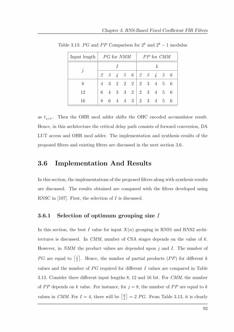
Chapter 3. RNS-Based Fixed Coefficient FIR Filters
Table 3.13: PG and PP Comparison for 2k and 2k − 1 modulus
Input length PG for NMM PP for CMM
jI k
2 3 4 5 6 2 3 4 5 6
8 4 3 2 2 2 2 3 4 5 6
12 6 4 3 3 2 2 3 4 5 6
16 8 6 4 4 3 2 3 4 5 6
as tLUT
. Then the OHR mod adder shifts the OHC encoded accumulator result.
Hence, in this architecture the critical delay path consists of forward conversion, DA
LUT access and OHR mod adder. The implementation and synthesis results of the
proposed filters and existing filters are discussed in the next section 3.6.
3.6 Implementation And Results
In this section, the implementations of the proposed filters along with synthesis results
are discussed. The results obtained are compared with the filters developed using
RNSC in [107]. First, the selection of I is discussed.
3.6.1 Selection of optimum grouping size I
In this section, the best I value for input X(n) grouping in RNS1 and RNS2 archi-
tectures is discussed. In CMM, number of CSA stages depends on the value of k.
However, in NMM the product values are depended upon j and I. The number of
PG are equal to⌈jI
⌉. Hence, the number of partial products (PP ) for different k
values and the number of PG required for different I values are compared in Table
3.13. Consider three different input lengths 8, 12 and 16 bit. For CMM, the number
of PP depends on k value. For instance, for j = 8, the number of PP are equal to k
values in CMM. For I = 4, there will be⌈84
⌉= 2 PG. From Table 3.13, it is clearly
92
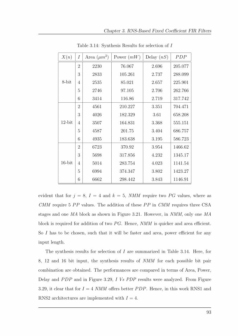
Chapter 3. RNS-Based Fixed Coefficient FIR Filters
Table 3.14: Synthesis Results for selection of I
X(n) I Area (µm2) Power (mW ) Delay (nS) PDP
8-bit
2 2230 76.067 2.696 205.077
3 2833 105.261 2.737 288.099
4 2535 85.021 2.657 225.901
5 2746 97.105 2.706 262.766
6 3414 116.86 2.719 317.742
12-bit
2 4561 210.227 3.351 704.471
3 4026 182.329 3.61 658.208
4 3507 164.831 3.368 555.151
5 4587 201.75 3.404 686.757
6 4935 183.638 3.195 586.723
16-bit
2 6723 370.92 3.954 1466.62
3 5698 317.856 4.232 1345.17
4 5014 283.754 4.023 1141.54
5 6994 374.347 3.802 1423.27
6 6662 298.442 3.843 1146.91
evident that for j = 8, I = 4 and k = 5, NMM require two PG values, where as
CMM require 5 PP values. The addition of these PP in CMM requires three CSA
stages and one MA block as shown in Figure 3.21. However, in NMM, only one MA
block is required for addition of two PG. Hence, NMM is quicker and area efficient.
So I has to be chosen, such that it will be faster and area, power efficient for any
input length.
The synthesis results for selection of I are summarized in Table 3.14. Here, for
8, 12 and 16 bit input, the synthesis results of NMM for each possible bit pair
combination are obtained. The performances are compared in terms of Area, Power,
Delay and PDP and in Figure 3.29, I Vs PDP results were analyzed. From Figure
3.29, it clear that for I = 4 NMM offers better PDP . Hence, in this work RNS1 and
RNS2 architectures are implemented with I = 4.
93
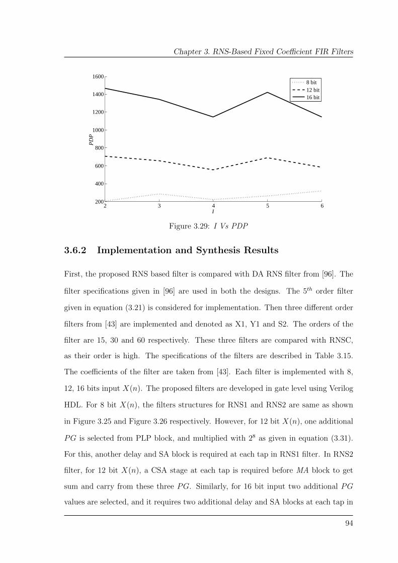
Chapter 3. RNS-Based Fixed Coefficient FIR Filters
2 3 4 5 6200
400
600
800
1000
1200
1400
1600
I
PD
P
8 bit12 bit16 bit
Figure 3.29: I Vs PDP
3.6.2 Implementation and Synthesis Results
First, the proposed RNS based filter is compared with DA RNS filter from [96]. The
filter specifications given in [96] are used in both the designs. The 5th order filter
given in equation (3.21) is considered for implementation. Then three different order
filters from [43] are implemented and denoted as X1, Y1 and S2. The orders of the
filter are 15, 30 and 60 respectively. These three filters are compared with RNSC,
as their order is high. The specifications of the filters are described in Table 3.15.
The coefficients of the filter are taken from [43]. Each filter is implemented with 8,
12, 16 bits input X(n). The proposed filters are developed in gate level using Verilog
HDL. For 8 bit X(n), the filters structures for RNS1 and RNS2 are same as shown
in Figure 3.25 and Figure 3.26 respectively. However, for 12 bit X(n), one additional
PG is selected from PLP block, and multiplied with 28 as given in equation (3.31).
For this, another delay and SA block is required at each tap in RNS1 filter. In RNS2
filter, for 12 bit X(n), a CSA stage at each tap is required before MA block to get
sum and carry from these three PG. Similarly, for 16 bit input two additional PG
values are selected, and it requires two additional delay and SA blocks at each tap in
94

Chapter 3. RNS-Based Fixed Coefficient FIR Filters
Table 3.15: Specification of Filters
Filters N ωp ωs δp δs
X1 15 0.2π 0.8π 0.0001 0.0001
Y1 30 0.3π 0.5π 0.00316 0.00316
S2 60 0.042π 0.14π 0.012 0.001
RNS1 filter. Hence in RNS1 filter, the delay and SA blocks are equal to the number
of PG. In RNS2, for 16 bit input, a two-stage CSA is required before MA block. In
RNS1 delay and MA, blocks are proportional to PG, hence it requires larger area as
compared to RNS2. In RNS1 and RNS2 delay, elements are realized using D-flipflops.
The filters are synthesized in UMC 90 nm technology using Cadence RTL compiler.
The performances of the filters are compared in terms of area, delay, power and power
delay product (PDP ). The synthesis results of 5th order filter given in equation (3.21)
are shown in Table 3.16. Both these filters are implemented without the reverse
converter. In both these implementations j and k are considered as 3 bits each as
given in [96]. The proposed architecture shows 21.31% and 24.64% improvement in
area and power gain respectively as compared to the methods reported in [96]. The
critical delays of both these circuits are similar. In the proposed filter I is considered
as 3, so the PLP block stores 8 words for each modulus. Hence, for a 5 tap filter,
each modulus requires 40 word PLP . At each tap, the stored inner product values
are accessed from PLP and are directly given to the SA block. Here, CSA stages
and MA are not required as the input size j and I both are equal. At each tap, M2
moduli set stores {3, 3, 4} bits. Hence, for a 5 tap filter, 50 bit registers are required
in the proposed design. The size of each SA is {3, 3, 4} bit adders for M2. So, the
proposed architecture for a 5 tap required 50, 1 bit full adders.
The filter structure is similar to the either of the architectures shown in Figure
95

Chapter 3. RNS-Based Fixed Coefficient FIR Filters
Table 3.16: Synthesis Results of RNS DA and Proposed RNS based FIR Filters
Filter Area Area Power Power Delay Dealy
(mm2) gain (%) (mW ) gain (%) (ns) gain (%)
[96] 3495 - 0.200607 - 3.977 -
Proposed 2750 21.31 0.151163 24.64 3.844 2.087
3.25, and Figure 3.26. This is due to the small size input. In [96], as the input to
be represented in TC, this architecture requires a forward converter. It first converts
the binary input into residues and encodes to equivalent TC number. Each modulus
requires different OHR mod adders, and the sizes of these adders are given in Table
3.11. For k = 3, the moduli set {5, 7, 8} requires 15, 21 and 24 2:1 multiplexers.
The present and past input samples are represented in TC format for each modulus.
Hence, for a 5 tap filter, modulus-5 requires 25 bit registers. Similarly, modulus-
7and 8 requires 37 and 43 registers respectively. And this architecture requires extra
hardware for clock divide circuits as each modulus modulo adder is different. Hence,
the proposed filter shows better results in terms of area and power. So far, the results
are compared for the smaller dynamic range. Now, the proposed architectures are
compared with RNSC filters, where filters require larger dynamic range.
The synthesis results of X1, Y1 and S2 obtained from cadence RTL compiler are
summarized in Table 3.17. Here k is the moduli selection, which is chosen such that
the filter output lies within the maximum range of moduli set. From Figure 3.24, the
critical delay path for RNSC consists of a forward converter, CMM along with SA
and end around carry addition. As shown in Figure 3.25, modular multiplication in
RNS1 consists simply PG selections from PLP and SA block, hence the critical delay
path consists, reverse converter at most. In RNS2, it consists CMM and SA along
with the end around carry addition. From the critical delay path analysis, RNS1 has
96

Chapter 3. RNS-Based Fixed Coefficient FIR Filters
Table 3.17: Synthesis Results of Proposed RNS based FIR Filters
Filter Input k MethodArea Area Delay Delay Power Power PDP PDP
(mm2) gain(%) (ns) gain(%) (mW ) gain(%) gain(%)
X1
8-bit 6
RNSC 0.0432 9.17 2.226 20.4
RNS1 0.0309 28.46 6.01 34.38 2.027 8.92 12.19 40.242
RNS2 0.0261 39.71 6.88 24.92 1.486 33.24 10.22 49.889
12-bit 8
RNSC 0.0772 10.9 4.49 49.08
RNS1 0.0582 24.58 6.98 36.15 3.702 17.55 25.84 47.356
RNS2 0.0485 37.16 8.49 22.37 2.553 43.13 21.67 55.855
16-bit 9
RNSC 0.0864 12.3 6.103 75.25
RNS1 0.0832 3.767 7.57 38.63 5.297 13.20 40.08 46.735
RNS2 0.0691 20.09 9.03 26.78 3.85 36.91 34.76 53.808
Y1
8-bit 7
RNSC 0.0969 9.44 5.041 47.58
RNS1 0.0726 25.12 6.47 31.43 4.593 8.87 29.73 37.517
RNS2 0.0615 36.52 7.46 20.96 3.629 28.01 27.08 43.097
12-bit 8
RNSC 0.1374 10.9 8.817 96.3
RNS1 0.1123 18.32 7.19 34.13 7.113 19.32 51.17 46.865
RNS2 0.0952 30.75 8.74 20.01 5.87 33.43 51.28 46.755
16-bit 9
RNSC 0.1674 12.7 12.2 154.5
RNS1 0.1558 6.958 7.51 40.64 9.906 18.80 74.44 51.806
RNS2 0.1348 19.49 9.31 26.48 8.455 30.69 78.69 49.052
S2
8-bit 7
RNSC 0.2506 9.5 12.52 119
RNS1 0.151 39.75 6.5 31.62 9.565 23.62 62.13 47.777
RNS2 0.129 48.52 7.6 20.01 8.065 35.60 61.28 48.487
12-bit 9
RNSC 0.4046 12.3 25.35 311.9
RNS1 0.2611 35.47 7.7 37.41 15.87 37.41 122.2 60.832
RNS2 0.2372 41.36 9.65 21.56 14.8 41.62 142.8 54.211
16-bit 10
RNSC 0.4567 12.9 34.27 443.6
RNS1 0.3756 17.75 8.17 36.91 24.3 29.08 198.4 55.264
RNS2 0.3099 32.13 10.5 19.25 20.25 40.90 211.7 52.283
97

Chapter 3. RNS-Based Fixed Coefficient FIR Filters
a better delay gain as compared to RNSC and RNS2. From Table 3.17, X1 filter using
RNS1 architecture achieves a delay gain of 34.39%, 36.16% and 38.63% as compared
to RNSC for 8, 12 and 16 bit inputs respectively. Similarly from Table 3.17, Y1
and S2 filters implemented with RNS1 architecture achieve a delay gain of 31.43%,
34.13%, 40.65% and 31.62%, 37.41%, 36.92% respectively as compared to RNSC for
8, 12 and 16-bit inputs. It can also observed from Table 3.17, that RNS2 filters
shows improvement in delay gain as compared to RNSC. However, with comparison
to RNS1, the delay gains of RNS2 filters are slightly smaller.
In RNS1, at each tap delay and SA blocks are equal to number of PG groups.
For 8, 12 and 16 bit inputs, the number of PG from equation (3.31) are 2, 3 and 4
respectively. Hence, for a 8 bit input, two delay and SA blocks are required. This
is shown in Figure 3.25 as two inputs to delay and SA block. In RNS2, as shown
in Figure 3.26 MA block is used at each tap for adding two PG selected from PLP
block. Thus the area and power consumption by RNS1 architecture is larger than
RNS2 architecture. Table 3.17 shows the area gains of X1, Y1, S2 filters implemented
with RNS2 architecture are 39.71%, 37.16%, 20.09% and 36.52%, 30.75%, 19.49%
and 48.52%, 41.36%, 32.13% respectively as compared to RNSC for 8, 12 and 16 bit
inputs. However, filters implemented using RNS1 architecture also has a comparable
area gain with respect to RNSC architectures. Similarly, power gain results are also
summarized in Table 3.17. It clearly shows that filters using RNS2 architecture
achieve a higher power gain as compared to RNS1.
For better synthesis analysis, RNS1 and RNS2, architectures are compared in-
terms of PDP and PDP gain. From Table 3.17, it is observed that delay of RNS1
and RNS2 architectures for any filter is based on k value. The k value is chosen as
9 for a 16 bits input filters X1, Y1 and for a 12 bit input filter S2. The delay of X1
filter using RNS1, RNS2 is 7.57 ns and 9.03 ns, respectively for k = 9. Similarly,
the delay values for Y1 are 7.51 ns, 9.31 ns and for S2 are 7.7 ns, 9.65 ns. The above
values show the delay is almost consistent for a given k, and it is independent of filter
98

Chapter 3. RNS-Based Fixed Coefficient FIR Filters
Sine Wave2
Sine Wave1
SignalTap II Logic AnalyzerSignal Compiler
Scope
Resource Usage
Logic: 56 % RAM: 0 %
Multiplier: 0 %
Output
o30:0Input
i15:0
Idealized ADC quantizer(settings: 16−bit converter
Vmin: 0, Vmax: 3.3)
A D
16 bits
HDL Import
x(15:0)reset y(30:0)RNS2_16bit_S2
GND
0
Cyclone II DE1 Development Board
Clock
6 ns
Figure 3.30: Filter Implementation in Altera DSP Builder
order and input length of the filter. Hence PDP value depends on the filter order as
well as input length.
The PDP and PDP gain values are also summarized in Table 3.17. For the same
k = 9, filter X1 of 15 order using RNS2 architectures achieve a PDP gain of 53.808%
as compared to RNSC. However, PDP gain of RNS1 is smaller than RNS2. As the
filter order increases for filter Y1 and S2, PDP gain of RNS1 increases. Filter Y1,
S2 of 30, 60 - order implemented using RNS1 architecture achieves a PDP gain of
51.806% and 60.832%. For k = 6 and 7, the PDP gain in any filter is high for RNS2
and for k = 8, X1 filter using RNS1 has larger gain and in Y1 filter, both RNS1 and
RNS2 are having a comparable gain. The analysis of PDP gain results from Table
3.17 shows that, increase in order and k value RNS1 filter architecture obtains larger
gain and for lower order filter and small k values, RNS2 architecture has larger gains.
3.6.3 Functional Verification
In this section, the functionality of the proposed filters is discussed. The implemen-
tation shown in Figure 3.30 is done using Altera DSP builder and is illustrated for
S2 filter type.
The functional verification of the filters is as follows:
99
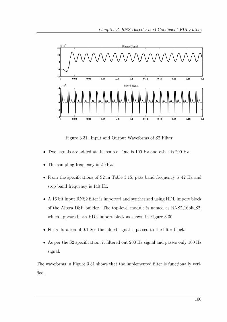
Chapter 3. RNS-Based Fixed Coefficient FIR Filters
0 0.02 0.04 0.06 0.08 0.1 0.12 0.14 0.16 0.18 0.2−5
0
5
10
15x 107
Filtered Signal
0 0.02 0.04 0.06 0.08 0.1 0.12 0.14 0.16 0.18 0.2−4
−2
0
2
4x 10⁴ Mixed Signal
Figure 3.31: Input and Output Waveforms of S2 Filter
• Two signals are added at the source. One is 100 Hz and other is 200 Hz.
• The sampling frequency is 2 kHz.
• From the specifications of S2 in Table 3.15, pass band frequency is 42 Hz and
stop band frequency is 140 Hz.
• A 16 bit input RNS2 filter is imported and synthesized using HDL import block
of the Altera DSP builder. The top-level module is named as RNS2 16bit S2,
which appears in an HDL import block as shown in Figure 3.30
• For a duration of 0.1 Sec the added signal is passed to the filter block.
• As per the S2 specification, it filtered out 200 Hz signal and passes only 100 Hz
signal.
The waveforms in Figure 3.31 shows that the implemented filter is functionally veri-
fied.
100

Chapter 3. RNS-Based Fixed Coefficient FIR Filters
3.7 Conclusion
In this chapter, a novel approach towards implementing a fixed coefficient FIR fil-
ter architecture in RNS has been presented. Modular multiplications, which is the
most intensive part of an RNS based filter, have been replaced by employing PLP
blocks. This reduced the number of partial products for the modular multiplier. The
accumulated partial products are added using shift and add approach owing to the
chosen moduli set {2k − 1, 2k, 2k+1 − 1}. Implementing PLP blocks also eliminates
the need for forward conversion. These blocks offer significant advantages in terms
of delay and area. Proposed filter implementation of different order shows significant
improvement in PDP gain.
101

Chapter 4
Programmable FIR Filters
The design and implementations for fixed coefficient FIR filters are discussed in chap-
ter 2 and 3. In some applications such as adaptive pulse shaping, filter banks in SDR
and signal equalization, requires adaptive filter coefficient sets. In these kind of filter
implementations, the filter building blocks (e.g. multiplier and adder) are independent
of coefficient set. Hence, these filters are implemented with the dedicated multipliers,
and these are known as programmable FIR filters. This chapter presents an approach
for implementing high speed programmable FIR filter architecture.
This chapter is organized as follows: section 4.1 presents the introduction to
programmable FIR filter implementations. In section 4.2, the architecture of the
proposed programmable FIR filter is discussed. The synthesis results of the proposed
architecture and it’s functional verification using Altera DSP builder is discussed in
section 4.3, followed by the conclusion in section 4.4.
4.1 Introduction to Programmable FIR Filter
The TDF structure is widely used in many FIR filter applications due to its higher
operating clock frequency as comapred to the DF structure. The filter equation (1.1),
implemented in TDF is shown in Figure 2.3. For convenience the filter equation is
given below
Y (n) =N−1∑k=0
hk ∗X(n− k) (4.1)
The adders in the filter shown in Figure 2.3 are used for accumulation, and these
are named as structural adder (SA). The SA adder cost is equal to the order of the
102
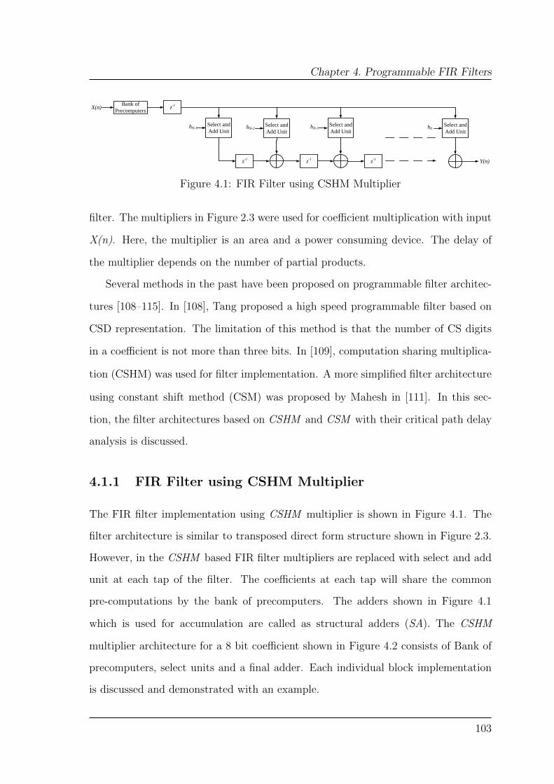
Chapter 4. Programmable FIR Filters
z-1
X(n)Bank of
Precomputers
Select and
Add UnithN-1
Select and
Add UnithN-2
z-1
Select and
Add UnithN-3
z-1
Select and
Add Unith0
Y(n)
z-1
Figure 4.1: FIR Filter using CSHM Multiplier
filter. The multipliers in Figure 2.3 were used for coefficient multiplication with input
X(n). Here, the multiplier is an area and a power consuming device. The delay of
the multiplier depends on the number of partial products.
Several methods in the past have been proposed on programmable filter architec-
tures [108–115]. In [108], Tang proposed a high speed programmable filter based on
CSD representation. The limitation of this method is that the number of CS digits
in a coefficient is not more than three bits. In [109], computation sharing multiplica-
tion (CSHM) was used for filter implementation. A more simplified filter architecture
using constant shift method (CSM) was proposed by Mahesh in [111]. In this sec-
tion, the filter architectures based on CSHM and CSM with their critical path delay
analysis is discussed.
4.1.1 FIR Filter using CSHM Multiplier
The FIR filter implementation using CSHM multiplier is shown in Figure 4.1. The
filter architecture is similar to transposed direct form structure shown in Figure 2.3.
However, in the CSHM based FIR filter multipliers are replaced with select and add
unit at each tap of the filter. The coefficients at each tap will share the common
pre-computations by the bank of precomputers. The adders shown in Figure 4.1
which is used for accumulation are called as structural adders (SA). The CSHM
multiplier architecture for a 8 bit coefficient shown in Figure 4.2 consists of Bank of
precomputers, select units and a final adder. Each individual block implementation
is discussed and demonstrated with an example.
103

Chapter 4. Programmable FIR Filters
1XX(n)
1001X (9X)
1011X (11X)
111X (7X)
1101X (13X)
101X (5X)
1111X (15X)
11X (3X)
Shifter
8:1
MUX
Ishifter AND
Select Unit
Shifter
8:1
MUX
Ishifter AND
Select Unit
Final
Adder
Product
X*h
Coefficient
h = 11011010
hL = 1010
hU = 1101
select010
shift01
101X 1010X
select110
shift00
1101X 1101X<<4Bank Of
Precomputers
Select and Add Unit
Figure 4.2: CSHM Multiplier
4.1.1.1 Bank of Precomputers
The precomputaion block architecture is shown in Figure 4.3. This block will pre-
compute the possible product values of the input X(n) using shift and add approach.
In this method, the coefficient is divided into the groups of four bits each [109]. Hence,
in each group the value of the coefficient ranges from 0 to 15. So this block has to
pre-compute the possible product values {0X, 1X, 2X, 3X, 4X, 5X, 6X, 7X, 8X,
9X, 10X, 11X, 12X, 13X, 14X, 15X}. Here, X is the input X(n). However, these
computations can be minimized by using the select unit, which will be discussed
104

Chapter 4. Programmable FIR Filters
X(n)
1001X (9X)
1011X (11X)
111X (7X)
1101X (13X)
101X (5X)
1111X (15X)
11X (3X)
1X
3X = 1X<<1 + X
5X = 1X<<2 + X
7X = 1X<<3 - X
9X = 1X<<3 + X
11X = 1X<<3 + 3X
13X = 1X<<3 + 5X
15X = 1X<<4 - 1X
1X<<1 = 2X
1X<<2 = 4X
1X<<3 = 8X
1X<<4 = 16X
Figure 4.3: Bank of Precomputers
in section 4.1.1.2. Here, {2X, 4X, 8X} can be omitted, since these values can be
obtained by simply shifting the value 1X by 1, 2 and 3 times respectively. Similarly,
{6X, 12X} can be obtained by shifting 3X and 10X is by shifting 5X and 14X can
be obtained by shifting 7X. Hence, this block calculates only the product values {1X,
3X, 5X, 7X, 9X, 11X, 13X, 15X} by using shift and add approach. There are seven
adders required for the precomputation block implementation as shown in Figure 4.3.
4.1.1.2 Select Unit
The select unit shown in Figure 4.2 consists of Shifter, 8:1 multiplexer, Ishifter and
an AND gate. The shifter circuit is used to generate the select and shift signals
for 8:1 multiplexer and ishifter circuits respectively. The input to the shifter is 4
bit value, which is derived from the coefficient. The input and output relation for
a shifter circuit is shown in Table 4.1. The select signal from the shifter is used
to select the product value from precomputer block through 8:1 multiplexer. The
ishifter circuit shifts the output from the multiplexer depending on shift signal from
105

Chapter 4. Programmable FIR Filters
Table 4.1: Shifter Circuit
Shifter
Input OutputshL or hH Shift Select
0000 00 0000001 00 0000010 01 0000011 00 0010100 10 0000101 00 0100110 01 0010111 00 0111000 11 0001001 00 1001010 01 0101011 00 1011100 10 0011101 00 1101110 01 0111111 00 111
the shifter circuit where as AND gate is used for the zero coefficient input.
The multiplication of input X with the coefficient can be expressed as in equation
(4.2)
X × h = X ×
dn4−1e∑l=0
hl × 24l
(4.2)
where, n is the number of bits to represent the filter coefficient h and l is the number of
4 bit coefficient groups. For n = 8, only two product values are required as compared
to eight partial products. Similarly for a 12, 16 bit coefficient 3 and 4 product values
are required instead of 12 and 16 partial products respectively. Hence the number of
partial products are reduced in CSHM multiplier architecture. The CSHM multiplier
is demonstrated in example 4.1.1.
Example 4.1.1. The CSHM multiplier is explained with the help of example. Con-
sider the filter coefficient h = 11011010. Now divide the coefficient into two groups
106

Chapter 4. Programmable FIR Filters
hL = 1010b = 10d and hU = 1101b = 13d and give as the inputs to select units as
shown in Figure 4.2. By referring to Table 4.1, the shifter circuit produces select as
010 and shift as 01 for the input hL. These values indicate that, the 8:1 multiplexer
will select 101Xb = 5Xd from the bank of precomputers and it should be shifted by
one time to get 1010Xb = 10Xd. The AND gate will pass the same value as the hL is
non-zero. Similarly, for hU the select value is 110 and shift value is 00. Hence, the 8:1
multiplexer chooses the product value as 1101Xb = 13Xd. Here ishifter doesn’t shift
the product value as the shift signal is 00. However, for obtaining the final product
value X × h, the hu × x should be shifted by 4 bits as given in equation (4.2) and
added with hl ×X with the help of final adder.
The critical path delay of this filter is one select and add unit, one SA. Here, for
a n bit coefficient the critical path delay in [109], is as given in equation (4.3).
Tcshm = Tshifter + Tishifter + T8:1mux +⌈log2
(n4
)⌉Tadd + TSA (4.3)
Here in equation (4.3), Tcshm is the critical path delay of the FIR filter architecture
proposed in [109]. Tshifter, Tishifter, T8:1mux, Tadd, and TSA are the delays of the shifter,
ishifter, 8:1 multiplexer, final adder and SA respectively. Two adder stages are re-
quired for a 16 bit coefficient to add four product values. Next section presents CSM
architecture proposed by Mahesh and Vinod which is an improvement over CSHM
architecture.
4.1.2 FIR Filter using Constant Shift Method (CSM )
The FIR filter implementation using CSM approach is shown in Figure 4.4. This
architecture consists of shift and add unit, processing element (PE), delay blocks and
adder. The adder is used for accumulating the previous tap product value. This
also referred as structural adder (SA). All these blocks are explained in detail in the
following sections.
107

Chapter 4. Programmable FIR Filters
Z-1
X(n)Shift and Add
Unit
PEhN-1 PEhN-2
Z-1
PEhN-3
Z-1
PEh0
Y(n)
Figure 4.4: FIR Filter using CSM
X(n)
101X (5X)
110X (6X)
100X (4X)
111X (7X)
11X (3X)
10X (2X)
1X
2X = 1X<<1
3X = 1X<<1 + X
4X = 1X<<2
5X = 1X<<2 + X
6X = 3X<<1
7X = 5X +2X
Figure 4.5: Shift and Add Unit
4.1.2.1 Shift and Add Unit
The shift and add unit shown in Figure 4.4 is similar to the bank of precomputers
in CSHM architecture. However, in CSM the coefficient is divided into a group of
3 bits each. Each group value ranges from 000b = 0d to 111b = 7d. Hence, the
shift and add unit will compute only {0X, 1X, 2X, 3X, 4X, 5X, 6X, 7X}. The shift
and add unit is shown in Figure 4.5. This architecture requires only three adders, as
compared to the bank of precomputers in CSHM architecture which requires seven
adders. This shows that area is reduced for shift and add unit as compared to the
bank of precomputers.
108

Chapter 4. Programmable FIR Filters
Inputs from Shift
and Add Unit LUT
Selection
Unit
h
MUX1 MUX2 MUX3 MUX4 MUX5 MUX6
r1 r2 r3 r4 r5 r6
<< 3 << 6 << 9 << 12 << 15
2:1
Multiplexer
Two’s
Complement
Output to SA
MA1 MA2 MA3
MA4
MA5
Shifter
Unit
Adder
Unit
Multiplier Adders
(MA) Sum1 ~Sum1
Sign bit
Sum
Figure 4.6: Processing Element for a 16 bit Coefficient
4.1.2.2 Processing Element (PE)
The PE of CSM approach is shown in Figure 4.6. The PE consists of selection unit,
shifter unit and adder unit. The selection unit consists of⌊n3
⌋8 : 1 multiplexers and
one 2|n|3 : 1 multiplexer. The inputs to this multiplexer are from shift and add unit,
and the select signals are from the coefficient stored in LUT. The shifter unit shifts
the selected product values from multiplexers as shown in Figure 4.6. The adder unit
adds all these shifted product values with the help of adders. These adders are called
as multiplier adders(MA). The output of final MA (i.e MA5 ) is Sum1. The two’s
complement circuit shown in Figure 4.6 is used for negative number coefficients. The
109

Chapter 4. Programmable FIR Filters
output of complement circuit is represented as ∼Sum1. The 2:1 multiplexer selects
∼Sum1 for negative coefficient for which the sign bit is ‘1’. For a positive coefficient,
the sign bit is ‘0’ hence, Sum1 is selected and given to SA block as shown in Figure 4.6.
Since the coefficient is divided into a group of 3 bits, the selection unit in PE requires
8:1 multiplexer. Hence, CSM architecture is implemented without any shifter and
ishifter circuits as compared to CSHM architecture. However, the number of product
values will be increased due to a one-bit reduction in grouping.
The critical path delay for a n bit coefficient, in [111] is as given in equation (4.4).
Tcsm = Tsau + T8:1mux +⌈log2
(n3
)⌉Tadd + TSA (4.4)
In equation (4.4), Tcsm is the critical path delay of the FIR filter architecture
proposed in [111]. Tsau is the delay of shift and add unit. A 16 bit coefficient will
select six product values. The addition of all these product values will be done by
using three-stage adder. The precomputation block is optimized in terms of delay
and number of adders in [111] as compared to [109].
However, in CSM and CSHM architectures the critical path delay depends on
the number of adder stages required to add the product values and the delay of SA.
Hence, there is a possibility of improving the clock frequency or minimizing the delay
by replacing the adders with suitable arithmetic circuits. In section 4.2, the proposed
programmable FIR filter architecture is discussed.
4.2 Proposed FIR Filter Architecture
In this section, the proposed architecture and its basic blocks are discussed. The
proposed architecture is shown in Figure 4.7. It consists of a shift and add unit, a
modified processing element (MPE) for each coefficient, a structural compressor (SC)
along with two delay elements at each tap of the filter and finally an adder after the
last tap of the filter. The shift and add unit shown in Figure 4.7 is implemented as
110
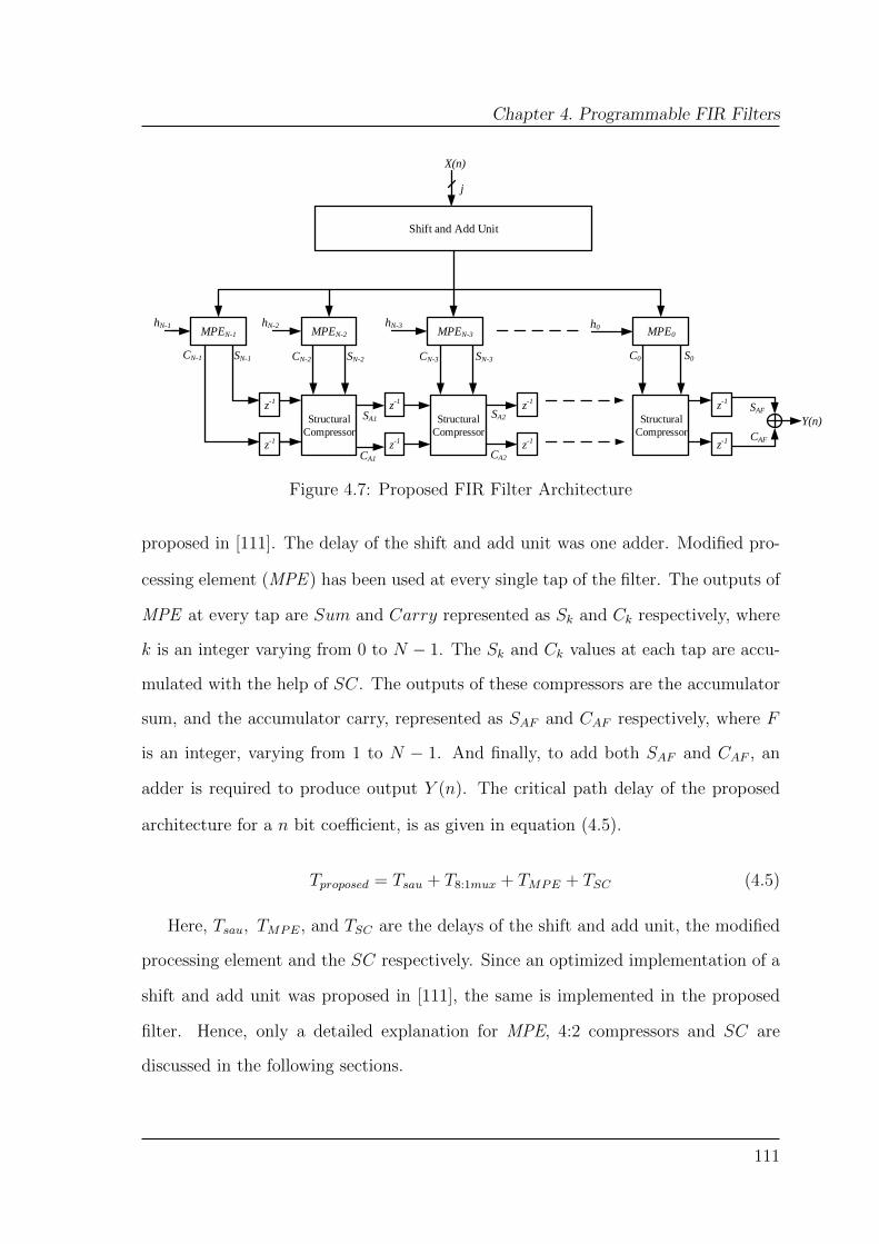
Chapter 4. Programmable FIR Filters
Shift and Add Unit
MPEN-1 MPEN-2 MPEN-3 MPE0
z-1
z-1
z-1
z-1
z-1
z-1
Structural
Compressor
Structural
Compressor
Structural
Compressor
j
hN-1 hN-2 hN-3 h0
X(n)
CN-1 SN-1 CN-2 SN-2 CN-3 SN-3 C0 S0
Y(n)
CA1 CA2
CAF
SA1 SA2
SAFz-1
z-1
Figure 4.7: Proposed FIR Filter Architecture
proposed in [111]. The delay of the shift and add unit was one adder. Modified pro-
cessing element (MPE ) has been used at every single tap of the filter. The outputs of
MPE at every tap are Sum and Carry represented as Sk and Ck respectively, where
k is an integer varying from 0 to N − 1. The Sk and Ck values at each tap are accu-
mulated with the help of SC. The outputs of these compressors are the accumulator
sum, and the accumulator carry, represented as SAF and CAF respectively, where F
is an integer, varying from 1 to N − 1. And finally, to add both SAF and CAF , an
adder is required to produce output Y (n). The critical path delay of the proposed
architecture for a n bit coefficient, is as given in equation (4.5).
Tproposed = Tsau + T8:1mux + TMPE + TSC (4.5)
Here, Tsau, TMPE, and TSC are the delays of the shift and add unit, the modified
processing element and the SC respectively. Since an optimized implementation of a
shift and add unit was proposed in [111], the same is implemented in the proposed
filter. Hence, only a detailed explanation for MPE, 4:2 compressors and SC are
discussed in the following sections.
111

Chapter 4. Programmable FIR Filters
4.2.1 Modified Processing Element (MPE) Architecture
The proposed MPE architecture for a 16 bit coefficient as shown in Figure 4.8 consists
of a selection unit and a compressor unit. The 16 bit coefficient is divided into 3 bits
of five groups and 1 bit of one group. Each group then selects a particular product
value from the shift and add unit. For a j bit input X(n), the shift and add unit has
a possibility of eight products values {0X, 1X, 2X, 3X, 4X, 5X, 6X, 7X}, each
of j + 3 bits. Hence, to select one product value, an 8:1 multiplexer is required for
five groups and a 2:1 multiplexer for 1 bit group. The 8:1 multiplexer are named as
MUX1 to MUX5 and the 2:1 multiplexer is MUX6. In Figure 4.8, MUX1 to MUX6
are considered as the selection unit. Each multiplexer input is fed from the shift and
add unit and the select signals will be from the coefficient bits which are stored in a
look-up table (LUT).
The outputs of MUX1 to MUX6 are represented as r1, r2, r3, r4, r5, r6 each of
j + 3 bits, respectively. Consider the input x is of j bits and the coefficient h is of n
= 16 bits. The multiplication of input with the coefficient can be obtained as given
in equation (4.6).
X × h = y =
dn3 e∑i=1
ri × 23×(i−1) (4.6)
In [111], output y can be obtained as shown in equation (4.7).
X × h = y = r1 + r2 × 23 + r3 × 26 + r4 × 29 + r5 × 212 + r6 × 215 (4.7)
To implement equation (4.7), five adders are required with logic depth (LD) of
three adders. Hence in equation (4.4),⌈log2
(n3
)⌉Tadd + TSA becomes 3Tadd + 1Tadd
resulting in a four stage adder delay. Since, shift and add unit requires one adder,
Tcsm in equation (4.4) requires 5Tadd and 1T8:1mux in critical path delay . In MPE,
as shown in Figure 4.8, r3 × 26, r4 × 29, r5 × 212 and r6 × 215 are given to the stage 1
112

Chapter 4. Programmable FIR Filters
Inputs from Shift and Add Unit
MUX3MUX2 MUX4 MUX5 MUX6
Compressor Stage2
MUXC MUXS
C S
<< 3 << 6 << 9 << 12 << 15
r1 r2 r3 r4 r5 r6
C1 S1
C2 S2
LUT
<< 1
S2'C2'
Selection
Unit
Compressor
Stage<< 1
C2 S2
MUX1
h
3 3 3 3 3 1
Compressor Stage1
j+3 j+3 j+3 j+3 j+3 j+3
j+3
j+18 j+18
j+19j+19
j+19 j+19
Figure 4.8: Modified Processing Element (MPE) Architecture
compressor which results S1 and C1. Next S1, C1 × 21, r1 and r2 × 23 are given to
the stage 2 compressor which results in S2 and C2. Depending on the sign bit, S2′ or
S2 from the MUXs and C2′ or C2 from MUXc can be chosen which results the final
sum S and carry C. Hence, the delay of TMPE is 2T4:2compressor which is faster than
3Tadd delay. These values will be accumulated with the next tap sum and carry of
the filter again by using a 4:2 compressor, as shown in Figure 4.7. Thus, the delay of
TMPE and TSC in equation (4.5) equals to three 4:2 compressors. Hence, for a 16 bit
113

Chapter 4. Programmable FIR Filters
coefficient the critical path delay in the proposed approach, requires 1Tadd for shift
and add unit, 1T8:1mux and 3T4:2compressor for MPE and SC which improved the delay
gain as compared to [111]. A detailed explanation of the compressor stage is given
below.
4.2.1.1 Compressor Stage
Compressor stage1 and compressor stage2 comprise the complete compressor stage.
The outputs of MUX3 to MUX6 are fed to compressor stage1. The outputs of stage1
are labeled as S1 and C1. The outputs of MUX1, MUX2, S1 and C1 are given to
compressor stage2 and the outputs are labeled as S2 and C2. Each compressor stage
consists of a half adder, a 3:2 compressor and a 4:2 compressor. For demonstration,
consider that j is of 8 bits, hence the outputs r1, r2, r3, r4, r5 and r6 are of 11
bits. The t3, t4, t5 and t6 in compressor stage1 shown in Figure 4.9, represents
r3×26, r4×29, r5×212 and r6×215, respectively. Zero padding is represented as 1′b0.
The outputs S1 and C1 are represented as given in equation (4.8)
S1 =
j+17∑m=0
S1m × 2m
C1 =
j+17∑m=0
C1m × 2m (4.8)
where m is an integer varying from 0 to j+17. The values of S1m and C1m are either
1 or 0. From Figure 4.9, S1 and C1 values for m = 0 to 5 are ‘0’only. Now S16, S17
and S18 are directly taken from 0, 1, and 2 bits of t3. Figure 4.9 shows that a half
adder is used to obtain S19, S110, S111 and C19, C110, C111, as the corresponding t5,
t6 are zeros. Similarly, a 3:2 compressor has been used for generating S112, S113, S114
and C112, C113, C114 bits. For S115 to S119 and C115 to C119 a 4:2 compressor is used.
For S120 and C120 a 3:2 compressor has been used. The carry in for this compressor
114

Chapter 4. Programmable FIR Filters
Dir
ect o
f va
lues
t6H
alf A
dder
3:2
com
pres
sor
4:2
Com
pres
sor
3:2
Com
pres
orH
alf A
dder
Dir
ect v
alue
s of
t3
1'b0
1'b0
1'b0
1'b0
1'b0
1'b0
1'b0
1'b0
1'b0
109
87
65
43
21
01'
b01'
b01'
b01'
b01'
b01'
b0r3
<<
6 =
t31'
b01'
b01'
b01'
b01'
b01'
b010
98
76
54
32
10
1'b0
1'b0
1'b0
1'b0
1'b0
1'b0
1'b0
1'b0
1'b0
r4<
<9
= t4
1'b0
1'b0
1'b0
109
87
65
43
21
01'
b01'
b01'
b01'
b01'
b01'
b01'
b01'
b01'
b01'
b01'
b01'
b0r5
<<
12 =
t5C
ompr
esso
r10
98
76
54
32
10
1'b0
1'b0
1'b0
1'b0
1'b0
1'b0
1'b0
1'b0
1'b0
1'b0
1'b0
1'b0
1'b0
1'b0
1'b0
r6<
<15
= t6
Stag
e1
S1 C1
Hal
f Add
er3:
2 co
mpr
esso
r4:
2 C
ompr
esso
r3:
2 C
ompr
esor
Hal
f Add
erD
irec
t val
ues
of t1
1'b0
1'b0
1'b0
1'b0
1'b0
1'b0
1'b0
S1
1'b0
1'b0
1'b0
1'b0
1'b0
1'b0
1'b0
1'b0
1'b0
C1
1'b0
1'b0
1'b0
1'b0
1'b0
1'b0
1'b0
1'b0
1'b0
1'b0
1'b0
1'b0
1'b0
109
87
65
43
21
01'
b01'
b01'
b0r2
<<
3 =
t2C
ompr
esso
r1'
b01'
b01'
b01'
b01'
b01'
b01'
b01'
b01'
b01'
b01'
b01'
b01'
b01'
b01'
b01'
b010
98
76
54
32
10
r1 =
t1St
age2
S2 C2
S125
S124
S123
S122
S121
S120
S119
S118
S117
S116
S115
S114
S113
S112
S1 11
S110
S19
S18
S17
S16
S15
S14
S13
S12
S11
S10
C1 25
C1 24
C1 23
C1 22
C1 21
C1 20
C1 19
C1 18
C1 17
C1 16
C1 15
C1 14
C1 13
C1 12
C1 11
C1 10
C1 9
C1 8
C1 7
C1 6
C1 5
C1 4
C1 3
C1 2
C1 1
C1 0
S125
S124
S123
S122
S121
S120
S119
S118
S117
S116
S115
S114
S113
S112
S1 11
S110
S19
S18
S17
S16
C1 25
C1 24
C1 23
C1 22
C1 21
C1 20
C1 19
C1 18
C1 17
C1 16
C1 15
C1 14
C1 13
C1 12
C1 11
C1 10
C1 9
C1 8
S226
S225
S224
S223
S222
S221
S220
S219
S218
S217
S216
S215
S214
S213
S212
S2 11
S210
S29
S28
S27
S26
S25
S24
S23
S22
S21
S20
C2 26
C2 25
C2 24
C2 23
C2 22
C2 21
C2 20
C2 19
C2 18
C2 17
C2 16
C2 15
C2 14
C2 13
C2 12
C2 11
C2 10
C2 9
C2 8
C2 7
C2 6
C2 5
C2 4
C2 3
C2 2
C2 1
C2 0
Fig
ure
4.9:
Sum
,C
arry
gener
atio
nusi
ng
Com
pre
ssor
Sta
ges
115

Chapter 4. Programmable FIR Filters
XOR XOR
2:1
Multiplexer
XOR
in1 in2 in3 in4
sumcarry
Cout
2:1
Multiplexer
Cin
XOR
10
10
Figure 4.10: Logic Diagram of 4:2 Compressor
is generated by the 4:2 compressor. Three MSB bits of S1 are the direct values of
t6 as shown in Figure 4.9. Similarly, S2 and C2 values are also shown in Figure 4.9.
Hence, the critical path delay to obtain S2 and C2 will consists of two stages 4:2
compressors.
The implementation of the half adder is using an ex-or (XOR) gate for the Sum
bit and an AND gate for Carry. A 3:2 compressor is a full adder that produces the
Sum with two XOR gates and Carry with three AND, two OR gates. In [106], a
4:2 compressor is implemented as shown in Figure 4.10. This compressor takes four
inputs in1, in2, in3, in4 along with previous stage carry(Cin) and give output in the
form of sum, carry along with carry out(Cout). Hence, sometimes it is also referred
as a 5:3 compressor [106]. By referring to Figure 4.10, it can be observed that Cout
does not depend upon Cin as it is available after 1 XOR and 1 2:1 multiplexer delay.
As a result, the delay of a 4:2 compressor will always be three times XORdelay.
116

Chapter 4. Programmable FIR Filters
4.2.1.2 Comparison of MPE
The delay of select and add unit (SADD) proposed in [109], processing element (PE )
in [111] and the proposed MPE are given in equations (4.9), (4.10) and (4.11) respec-
tively.
TSADD = Tshifter + Tishifter + T8:1mux +⌈log2
(n4
)⌉Tadd (4.9)
TPE = T8:1mux +⌈log2
(n3
)⌉Tadd (4.10)
TMPE = T8:1mux +{⌈
log2
(n3
)⌉− 1}T4:2compressor (4.11)
For a n = 16 bit coefficient, TSADD requires a two-stage adder, TPE requires a three-
stage adder, where as TMPE requires two-stage 4:2 compressor. The delay equations
for SADD, PE and MPE are derived from the Figures 4.2, 4.6 and 4.8 respectively.
The SADD, PE and MPE blocks are synthesized using Cyclone II device in Altera
DSP builder.
The synthesis results shown in Table 4.2 are compared in terms of resource usage
(RU ), delay, and delay gain. The RU is the ratio of logic cells utilized by the archi-
tecture to the total number of available logic cells of a device in terms of percentage
value. For convenience, RU values are rounded to the nearest integer. The delay of
MPE for j = 8, 12 and 16 bits are 2.476, 3.222 and 2.838ns respectively. A 4:2 com-
pressor delay is often less than an adder delay, hence in the proposed MPE, the delay
is considerably less as compared to the existing architectures as shown in Table 4.2.
In section 4.3, the synthesis environments along with complete filter implementation
are discussed in detail.
4.2.2 Structural Compressors (SC)
At every single tap of the filter, the outputs of MPE are accumulated with the earlier
tap S, C. Hence, at each tap, two outputs from MPE and two outputs from preceding
117

Chapter 4. Programmable FIR Filters
Table 4.2: Synthesis results of MPE
j Method RU Delay Delay Gain
8
SADD [109] 2 12.628
PE [111] 1 12.792 -1.29
MPE 1 2.476 80.64
12
SADD [109] 3 14.465
PE [111] 2 15.119 -4.52
MPE 2 3.222 77.72
16
SADD [109] 4 16.368
PE [111] 3 18.223 -11.33
MPE 2 2.838 82.66
tap MPE are available. To get sum and carry from these four values, again a 4:2
compressor is used and named as structural compressors (SC), as shown in Figure
4.7. There are two outputs from the SC, hence two registers are required to store
these values. This extra register will result as an increase in area of the filter.
4.3 Experimental Results
In this section, the synthesis results of the proposed filter architecture, with archi-
tectures of [109] and [111] are discussed. The filter specifications and coefficients are
taken from [43]. The filters are labeled as X1, Y 1, and L2, and the orders of the
filters are 15, 30, and 63, respectively. Normalized filter passband, stopband edge
frequencies (ωp, ωs) and passband, stopband ripple values (δp, δs) are given in Table
4.3. The filter architectures proposed in [109] and [111] are named as CSHM and
118

Chapter 4. Programmable FIR Filters
Table 4.3: Specifications of filters
Filter N ωp ωs δp δs
X1 [43] 15 0.2π 0.8π 0.0001 0.0001
Y1 [43] 30 0.3π 0.5π 0.00316 0.00316
L2 [43] 63 0.2π 0.28π 0.028 0.001
CSM respectively. The filters in Table 4.3, are implemented in Verilog HDL [79] us-
ing CSHM, CSM and with the proposed techniques for 8, 12 and 16 bit input word
lengths (WL). The filters are synthesized using Altera Quartus II 12.0 and the DSP
builder tool [116, 117]. The target device is the Cyclone II EP2C20F484C7 (DE1
development board), which is fabricated in 90 nm technology [118]. A carry look
ahead (CLA) adder is used in [111] wherever an adder is required. However, in [109],
square root select (SRS) adders were used instead of CLA, hence while implementing
CSHM, SRS adders are used. D-Flipflops are used as registers in all architectures.
The functional verification of the filters is checked through the DSP builder. For
demonstration, the proposed filter architecture for the L2 filter of 63 order and 8 bit
WL is shown in Figure 4.11. Consider that the sampling frequency (FT ) is 2 kHz.
From Table 4.3, the passband and the stopband edge frequencies (fp, fs) are 200
Hz and 280 Hz, respectively. This indicates that the L2 filter will pass frequencies
of up to 200 Hz. Hence in this implementation, two sine waves are considered and
named as Sine Wave1 and Sine Wave2 as shown in Figure 4.11. Sine Wave1 is of 800
Hz and Sine Wave2 is of 50 Hz. Both these signals are added and quantized to 8
bits through an ADC. Now this signal will pass through the L2FILTER, as shown in
Figure 4.11. The L2FILTER is implemented using Verilog gate-level description and
imported through HDL import of the DSP builder. As per L2 filter specifications, it
will pass frequencies below 200 Hz, hence the output from the L2FILTER consists of
119

Chapter 4. Programmable FIR Filters
a 50 Hz signal. The input and output signals are as noise signal and filtered signal
shown in Figure 4.12. Figure 4.12 clearly shows that the proposed filter architecture
produces 50 Hz signal. Thus the filters functionality is verified.
For logic cell utilization and critical path delay estimation, Resource usage block
is used as shown in Figure 4.11. Power estimation is done through Quartus II 12.0.
The clock frequency is 166.67 MHz (6 ns). The synthesis results of the filters are listed
in Table 4.4. The results are compared in terms of delay (D), power (P ) and power-
delay product (PDP ) along with their gains with respect to the CSHM architecture.
The resource usage (RU ) of the filter is also given in Table 4.4. For instance, with
the signal compiler after synthesizing, the Resource usage shows 21% of logic cells are
used for the L2FILTER as shown in Figure 4.11, with a delay of 3.85 ns. The same
values along with power consumption for this filter (L2 for an 8 bit WL) are shown
in Table 4.4.
In filterX1, the delay value for 8, 12 and 16 bitWL values are 11.26ns, 13.47ns and
16.39ns for the CSHM architecture, and for the CSM, the values are 10.96ns, 13.06ns
and 15.64ns respectively. However, for the proposed architecture, the delay values
are similar for 8, 12 and 16 bit WL. Hence, for X1 filter the proposed architecture
achieves a 62%, 75%, and 76% delay gain as compared to the CSHM architecture.
This is due to the use of 4:2compressors that have less delay as compared to SA.
In the proposed architecture, RU increases as the order of filter increases. This
is due to storing SAF and CAF values in two registers. This also leads to slight
increase in power consumption of the proposed filter. Hence, PDP is considered as
performance metric. From Table 4.4, the PDP gain for 8, 12, and 16 bit WL of X1
filter are 61.09%, 72.68%, and 74.53%, respectively. From the synthesis results it can
be observed that in CSHM and CSM architectures, the delay value increases as WL
increases. Hence, the synthesized results show that the proposed filter has significant
PDP and delay gain as compared to the CSHM and CSM architectures.
120

Chapter 4. Programmable FIR Filters
VC
C1
Sine
Wav
e2
Sine
Wav
e1
Sign
alT
ap I
I L
ogic
Ana
lyze
rSi
gnal
Com
pile
r
Scop
e7
Res
ourc
e U
sage
Log
ic:
21 %
R
AM
: 0
%
Mul
tiplie
r: 0
%
Out
put1
o26:
0
Inpu
ti7
:0
Idea
lized
AD
C q
uant
izer
(set
tings
: 8−
bit c
onve
rter
Vm
in: 0
, Vm
ax: 3
.3)
AD
8 bi
ts
HD
L I
mpo
rt
x(7:
0)re
set_
ny(
26:0
)L
2FIL
TE
R
Cyc
lone
II
DE
1 D
evel
opm
ent B
oard
Con
stan
t
2
Clo
ck6
ns
Fig
ure
4.11
:L
2F
ilte
rsy
nth
esiz
edin
DSP
Builder
121

Chapter 4. Programmable FIR Filters
050
100
150
200
250
300
350
400
0
0.51
1.52
x 10
6Fi
ltere
d Si
gnal
050
100
150
200
250
300
350
400
−20
0
−10
00
100
200
Noi
se S
igna
l
Fig
ure
4.12
:L
2F
ilte
rV
erifi
cati
on
122

Chapter 4. Programmable FIR Filters
Table 4.4: Synthesis Results
Filter WL Architecture RUDelay Delay Power Power
PDPPDP
(ns) gain (%) (mW) gain (%) gain (%)
X1
8
CSHM [109] 3 11.26 110.41 1243.33
CSM [111] 3 10.96 2.65 115.69 -4.78 1268.31 -2.01
Proposed 4 4.12 62.43 117.45 -6.38 483.78 61.09
12
CSHM [109] 4 13.47 116.15 1564.66
CSM [111] 4 13.06 3.09 120.84 -4.04 1577.57 -0.83
Proposed 6 3.36 75.09 127.35 -9.64 427.39 72.68
16
CSHM [109] 5 16.39 126.96 2080.24
CSM [111] 4 15.64 4.54 148.24 -16.76 2318.62 -11.46
Proposed 7 3.86 76.42 137.17 -8.04 529.89 74.53
Y1
8
CSHM [109] 7 11.25 140.57 1581.13
CSM [111] 6 11.37 -1.06 179.60 -27.77 2041.51 -29.12
Proposed 10 3.60 68.01 150.62 -7.15 541.93 65.73
12
CSHM [109] 9 14.18 150.22 2129.97
CSM [111] 8 13.31 6.16 185.03 -23.17 2461.82 -15.58
Proposed 12 3.76 73.47 175.00 -16.50 658.35 69.09
16
CSHM [109] 11 16.32 157.78 2574.34
CSM [111] 10 15.81 3.12 188.78 -19.65 2984.05 -15.92
Proposed 15 3.66 77.60 186.54 -18.23 681.80 73.52
L2
8
CSHM [109] 15 11.64 193.40 2250.21
CSM [111] 14 11.07 4.89 200.10 -3.46 2214.31 1.60
Proposed 21 3.85 66.94 231.70 -19.80 891.12 60.40
12
CSHM [109] 20 14.43 223.65 3227.05
CSM [111] 17 13.58 5.87 225.68 -0.91 3065.19 5.02
Proposed 27 4.27 70.39 227.47 -1.71 971.75 69.89
16
CSHM [109] 24 16.57 255.57 4233.77
CSM [111] 21 15.73 5.07 254.86 0.28 4007.93 5.33
Proposed 33 3.97 76.06 309.55 -21.12 1227.68 71.00
123

Chapter 4. Programmable FIR Filters
4.4 Conclusion
In this chapter, an approach for a high speed programmable FIR filter architecture for
faster applications is presented. A 4:2, and 3:2 compressors are used for implementing
MPE. This improved a delay gain in MPE as compared to conventional PE, where
adders are used. A 4:2 compressor is used as an SC to further make the filter delay
efficient with area overhead. As compressors are faster than adders, the proposed
architecture showed significant improvement in delay and PDP gain. One of the
proposed architecture shows a 62.43% delay gain and a 61.09% PDP gain as compared
to the existing filter architectures.
124

Chapter 5
Conclusions and Future Work
This thesis addressed the issues in FIR filter design and its implementation for fixed
and programmable coefficients. From the filter transfer function, it is observed that,
coefficient multiplication consumes most of the hardware in filter implementations.
The coefficient multiplication depends on the filter implementation type. Multipli-
erless realization using shift and add approach is one such famous implementation
for the fixed coefficient filter. In multiplierless implementations, the coefficient mul-
tiplication depends on the number of SPT terms present in a coefficient. Several
signal processing applications use RNS for achieving higher clock frequency. How-
ever, the use of RNS doesn’t guarantee an area and power efficient implementation. In
programmable filters dedicated multipliers were used and these multipliers are most
expensive in terms of hardware. In brief, this thesis addressed the following issues:
• Calculation of FIR filter coefficients with a minimum number of SPT terms
using optimization algorithms.
• An efficient RNS based fixed coefficient FIR filter implementation.
• Improvement in the clock frequency of programmable FIR filter implementa-
tions using appropriate arithmetic circuits.
This chapter summarizes and presents the tasks accomplished in this thesis. The
challenges and scope of future research work in filter design are also discussed.
125

Chapter 5. Conclusions and Future Work
5.1 Conclusions
As the first contribution, an approach to FIR filter design using DE algorithm is
proposed in the thesis. From the literature survey, it is understood that FIR filters
are designed with various optimization techniques. Several deterministic algorithms
such as linear programming and mixed integer linear programming have been used
in the past to obtain hardware efficient filter coefficients. At the same time, the
stochastic algorithms such as genetic and differential evolution (DE) have also been
used for filter design in the recent years. Few researchers have designed FIR filter with
DE algorithm for which the objective function is only to obtain the desired frequency
response of the filter [61, 62, 72]. However, these objective functions in [61, 62, 72] do
not focus on minimizing the number of SPT terms. In this thesis, a filter is designed
with the minimum number of SPT terms using DE algorithm. Furthermore, CSE
approach is applied to obtain filter coefficients that lead to a hardware efficient filter
implementation. The experimental results showed significant improvements in area,
delay, and power gain in comparison to some recent reported design methods. One of
the proposed filters showed maximum PDP gain of 29% than those designed using
Remez algorithm. The results of this study will lead to improvements in filter design
for specific application.
In the second contribution, an approach for RNS based fixed coefficient FIR fil-
ter structure is presented. In spite of its carry-free modulo arithmetic operations,
only few researchers have contributed in the field of RNS DA based FIR filter imple-
mentations. Many of these RNS based filters are designed with conventional moduli
set{
2k − 1, 2k, 2k + 1}
. The main issue in this moduli set is, 2k + 1 modulo scal-
ing operations. Recently, an RNS based FIR filter with inner product computation
was presented in [96]. This method overcomes the modulo scaling by encoding the
BC residues into TC and modulo adder design with OHR representation. The OHR
modulo adder presented in [96] is simple to design and modulo scaling was obtained
126

Chapter 5. Conclusions and Future Work
by simple shift operations. However, throughput of this design is less, and it requires
conversion between BC residues to TC encoding, OHR to BC encoding and requires
more registers for storing the previous inputs. The filter in [96] is best suited for
smaller dynamic ranges. However, selection of moduli set also plays a significant role
in RNS based filter design. The second major finding is the forward conversion, its
BC residue encoding and OHR to BC residue conversion. Hence, in this thesis two
RNS based FIR filter architectures using the moduli set{
2k − 1, 2k, 2k+1 − 1}
are
proposed. The modulus 2k + 1 is replaced with the modulus 2k+1−1, which increases
the dynamic range of the design and overcomes the modulo scaling operation. The
proposed architectures focus on the LUT based multipliers without forward conver-
sion. The proposed LUT based multipliers reduced the number of partial products as
compared to conventional modulo multiplication. The LUT stores pre-computed in-
ner products for each coefficient in RNS and thus, avoids forward conversion. Due to
parallel implementation, the throughput of the filter is increased as compared to [96].
The proposed filters are implemented in Verilog HDL and are synthesized in Cadence
RTL using the 90nm technology library. The filters with LUT based multipliers and
conventional multipliers are compared in-terms of area, power and delay. The RNS
filters with LUT based multipliers showed significant improvement in clock frequency,
area and power gain.
The third contribution of this thesis presents a high speed programmable FIR
filter architecture. The programmable filters are extensively used in several signal
processing applications such as SDR and DSP processors. These filter implementa-
tions use dedicated multipliers, which consume a lot of hardware. Few researchers
have addressed this issue in the past and proposed some novel approaches. Compu-
tation sharing multiplication is one such approach proposed in [109]. A pre-computer
block is used to calculate the possible product values with input. In this method,
the coefficient is divided into a group of 4 bits each. Each group selects the pre-
127
Chapter 5. Conclusions and Future Work
computed values and add these values using select and add circuit. A modification
to this approach is proposed in [111]. In [111], the coefficient is divided into a group
of 3 bits each instead of 4 bits as in [109]. This modification reduces the number of
pre-computed values and uses simple selection circuit. In either of these approaches,
at every tap of the filter, two adder stages are required. One for adding the final sum
and carry in the multiplier and second is for accumulating the previous tap values.
These two adder stages play an important role in the critical path delay. Hence,
in this thesis, a high speed programmable filter with the use of compressor circuits
is proposed. The compressors are fast in operation as compared to adders. In the
proposed filter design, the two adders at every tap of the filter are replaced with one
4:2 compressor, which improves the clock frequency of the filter. The proposed high
speed filters are synthesized in Altera Cyclone II devices. The filter functionality is
verified with DSP builder using Altera DE1 board. One of the proposed filter show
62.43% delay gain and 61.09% power-delay product gain as compared to the existing
architectures.
5.2 Future Work
In this thesis, the challenges in FIR filter design and its implementations for fixed
and programmable coefficients are discussed. Three approaches to tackle these issues
were proposed in this thesis. However, further research may continue and may be
undertaken to address the proposed challenges as follows:
Modified Differential Evolution Algorithm for FIR Filter
The DE algorithm generates good optimum results by choosing the suitable values
for parameters such as mutation, cross-over ratio and strategies. Among these, DE
follows six strategies, which are developed in general for various problems. However, a
future study developing a new strategy dedicated for FIR filter would be challenging.
128

Chapter 5. Conclusions and Future Work
Further study on DE algorithm for multirate filter bank would be an interesting
topic. In multirate filter bank, FIR filter is designed such that, the desired frequency
response should be obtained after decimation or interpolation. This will add more
constraints to the objective function and would be challenging with DE algorithm.
RNS Based FIR Filters
RNS in signal processing applications is widely used due to its carry-free arithmetic
operations. In this thesis, RNS based FIR filters are implemented using three moduli
set with LUT based multipliers. A limitation of this architecture is that dynamic
range of the moduli set should satisfy the filter design. Further research should focus
on filter design with four or more moduli set. The four and above moduli sets will
increase the dynamic range, hence it would be challenging to implement higher-order
filters with higher clock frequency.
Programmable FIR Filters
In this thesis, a high speed programmable filter is implemented using 4:2 compressors.
The use of compressors results in higher clock frequency. However, this implementa-
tion requires more area, for large-size input and coefficients. Further research could
significantly explore on programmable filter implementation with RNS. A future study
on selection of moduli sets, and its use in implementing the programmable filter would
be challenging.
129
References
[1] B. A. Shenoi, Introduction to Digital Signal Processing and Filter Design. Wi-
ley, India, 2005.
[2] C. Burrus and T. Parks, Digital Filter Design. Wiley, New York, 1987.
[3] E. C. Ifeachor and B. W. Jervis, Digital Signal Processing: A Practical Ap-
proach. Pearson, India, 2002.
[4] S. K. Mitra, Digital Signal Processing. TMH, India, 2006.
[5] B. Gold and K. Jordan Jr., “A direct search procedure for designing finite
duration impulse response filters,” IEEE Transactions on Audio and Electroa-
coustics, vol. 17, no. 1, pp. 33–36, 1969.
[6] L. Rabiner, B. Gold, and C. McGonegal, “An approach to the approximation
problem for nonrecursive digital filters,” IEEE Transactions on Audio and Elec-
troacoustics, vol. 18, no. 2, pp. 83–106, 1970.
[7] T. Parks and J. McClellan, “Chebyshev approximation for nonrecursive digital
filters with linear phase,” IEEE Transactions on Circuit Theory, vol. 19, no. 2,
pp. 189–194, 1972.
[8] J. McClellan, T. Parks, and L. Rabiner, “A computer program for designing
optimum FIR linear phase digital filters,” IEEE Transactions on Audio and
Electroacoustics, vol. 21, no. 6, pp. 506–526, 1973.
[9] B. Venkataramani, Digital Signal Processors. Tata McGraw-Hill Education,
2002.
130

REFERENCES
[10] H. Samueli, “An improved search algorithm for the design of multiplierless
FIR filters with powers-of-two coefficients,” IEEE Transactions on Circuits and
Systems, vol. 36, no. 7, pp. 1044–1047, 1989.
[11] K. K. Parhi, VLSI Digital Signal Processing. Wiley, India, 2007.
[12] M. Aktan, A. Yurdakul, and G. Dundar, “An algorithm for the design of low-
power hardware-efficient FIR filters,” IEEE Transactions on Circuits and Sys-
tems I: Regular Papers, vol. 55, no. 6, pp. 1536–1545, 2008.
[13] L. R. Rabiner, “The design of finite impulse response digital filters using linear
programming techniques,” Bell System Technical Journal, vol. 51, no. 6, pp.
1177–1198, 1972.
[14] J. McClellan and T. Parks, “A unified approach to the design of optimum FIR
linear-phase digital filters,” IEEE Transactions on Circuit Theory, vol. 20, no. 6,
pp. 697–701, 1973.
[15] D. Kodek, “Design of optimal finite wordlength FIR digital filters using integer
programming techniques,” IEEE Transactions on Acoustics, Speech and Signal
Processing, vol. 28, no. 3, pp. 304–308, 1980.
[16] Y. Lim and S. Parker, “FIR filter design over a discrete powers-of-two coefficient
space,” IEEE Transactions on Acoustics, Speech and Signal Processing, vol. 31,
no. 3, pp. 583–591, 1983.
[17] Q. Zhao and Y. Tadokoro, “A simple design of FIR filters with powers-of-two
coefficients,” IEEE Transactions on Circuits and Systems,, vol. 35, no. 5, pp.
566–570, 1988.
[18] Y. C. Lim, J. Evans, and B. Liu, “Decomposition of binary integers into signed
power-of-two terms,” IEEE Transactions on Circuits and Systems, vol. 38, no. 6,
pp. 667–672, 1991.
131

REFERENCES
[19] J. H. Lee, C. K. Chen, and Y. C. Lim, “Design of discrete coefficient FIR digital
filters with arbitrary amplitude and phase responses,” IEEE Transactions on
Analog and Digital Signal Processing,Circuits and Systems II, vol. 40, no. 7, pp.
444–448, 1993.
[20] D. Li, J. Song, and Y. C. Lim, “A polynomial-time algorithm for designing
digital filters with power-of-two coefficients,” in IEEE International Symposium
on Circuits and Systems, (ISCAS’93), vol. 1, 1993, pp. 84–87.
[21] A. Dempster and M. Macleod, “Use of multiplier blocks to reduce filter complex-
ity,” in IEEE International Symposium on Circuits and Systems, (ISCAS’94),
vol. 4, 1994, pp. 263–266.
[22] J. J. Shyu and Y. C. Lin, “A new approach to the design of discrete coefficient
FIR digital filters,” IEEE Transactions on Signal Processing, vol. 43, no. 1, pp.
310–314, 1995.
[23] D. Li, “Minimum number of adders for implementing a multiplier and its ap-
plication to the design of multiplierless digital filters,” IEEE Transactions on
Circuits and Systems II: Analog and Digital Signal Processing, vol. 42, no. 7,
pp. 453–460, 1995.
[24] W. J. Oh and Y. H. Lee, “Implementation of programmable multiplierless FIR
filters with powers-of-two coefficients,” IEEE Transactions on Circuits and Sys-
tems II: Analog and Digital Signal Processing, vol. 42, no. 8, pp. 553–556, 1995.
[25] A. Dempster and M. Macleod, “Use of minimum-adder multiplier blocks in
FIR digital filters,” IEEE Transactions on Circuits and Systems II: Analog and
Digital Signal Processing, vol. 42, no. 9, pp. 569–577, 1995.
132

REFERENCES
[26] R. Hartley, “Subexpression sharing in filters using canonic signed digit multipli-
ers,” IEEE Transactions on Circuits and Systems II: Analog and Digital Signal
Processing, vol. 43, no. 10, pp. 677–688, 1996.
[27] J. T. Kim, W. J. Oh, and Y. H. Lee, “Design of nonuniformly spaced linear-
phase FIR filters using mixed integer linear programming,” IEEE Transactions
on Signal Processing, vol. 44, no. 1, pp. 123–126, 1996.
[28] D. Parker and K. Parhi, “Area-efficient parallel FIR digital filter implementa-
tions,” in Proceedings of International Conference on Application Specific Sys-
tems, Architectures and Processors, (ASAP’96), 1996, pp. 93–111.
[29] Y. S. Song and Y. H. Lee, “Design of sparse FIR filters based on branch-and-
bound algorithm,” in Proceedings of 40th Midwest Symposium on Circuits and
Systems, (MWSCAS’97), vol. 2, 1997, pp. 1445–1448.
[30] N. I. Cho and S. U. Lee, “Optimal design of finite precision FIR filters using
linear programming with reduced constraints,” IEEE Transactions on Signal
Processing, vol. 46, no. 1, pp. 195–199, 1998.
[31] C. L. Chen and J. Willson, A.N., “A trellis search algorithm for the design
of FIR filters with signed-powers-of-two coefficients,” IEEE Transactions on
Circuits and Systems II: Analog and Digital Signal Processing, vol. 46, no. 1,
pp. 29–39, 1999.
[32] Y. C. Lim, R. Yang, D. Li, and J. Song, “Signed power-of-two term allocation
scheme for the design of digital filters,” IEEE Transactions on Circuits and
Systems II: Analog and Digital Signal Processing, vol. 46, no. 5, pp. 577–584,
1999.
133

REFERENCES
[33] J. Yli Kaakinen and T. Saramaki, “A systematic algorithm for the design of
multiplierless FIR filters,” in Proceeding of the IEEE International Symposium
on Circuits and Systems, (ISCAS’01), vol. 2, 2001, pp. 185–188.
[34] C. Y. Yao and C. J. Chien, “A partial milp algorithm for the design of linear
phase FIR filters with spt coefficients,” IEICE Transactions on Fundamentals
of Electronics, Communications and Computer Sciences, vol. 46, no. 1, pp.
2302–2310, 2002.
[35] Z. G. Feng and K. L. Teo, “A discrete filled function method for the design
of FIR filters with signed-powers-of-two coefficients,” IEEE Transactions on
Signal Processing, vol. 56, no. 1, pp. 134–139, 2008.
[36] F. Xu, C. H. Chang, and C. C. Jong, “Design of low-complexity FIR filters
based on signed-powers-of-two coefficients with reusable common subexpres-
sions,” IEEE Transactions on Computer-Aided Design of Integrated Circuits
and Systems, vol. 26, no. 10, pp. 1898–1907, Oct 2007.
[37] Y. J. Yu and Y. C. Lim, “Design of linear phase FIR filters in subexpression
space using mixed integer linear programming,” IEEE Transactions on Circuits
and Systems I: Regular Papers, vol. 54, no. 10, pp. 2330–2338, Oct 2007.
[38] H. Q. Ta and T. L. Nhat, “Design of FIR filter with discrete coefficients based
on mixed integer linear programming,” in Proceeding of the 9th International
Conference on Signal Processing, (ICSP 2008), Oct 2008, pp. 9–12.
[39] Z. G. Feng and K. L. Teo, “A discrete filled function method for the design
of FIR filters with signed-powers-of-two coefficients,” IEEE Transactions on
Signal Processing, vol. 56, no. 1, pp. 134–139, 2008.
134

REFERENCES
[40] Y. J. Yu, D. Shi, and Y. C. Lim, “Design of extrapolated impulse response FIR
filters with residual compensation in subexpression space,” IEEE Transactions
on Circuits and Systems I: Regular Papers, vol. 56, no. 12, pp. 2621–2633, 2009.
[41] Y. Yu and Y. Lim, “Optimization of linear phase FIR filters in dynamically ex-
panding subexpression space,” Circuits, Systems and Signal Processing, vol. 29,
no. 1, pp. 65–80, 2010.
[42] D. Kodek, “LLL algorithm and the optimal finite wordlength FIR design,”
IEEE Transactions on Signal Processing, vol. 60, no. 3, pp. 1493–1498, 2012.
[43] D. Shi and Y. J. Yu, “Design of linear phase FIR filters with high probability
of achieving minimum number of adders,” IEEE Transactions on Circuits and
Systems I: Regular Papers, vol. 58, no. 1, pp. 126–136, 2011.
[44] A. Shahein, Q. Zhang, N. Lotze, and Y. Manoli, “A novel hybrid monotonic
local search algorithm for FIR filter coefficients optimization,” IEEE Transac-
tions on Circuits and Systems I: Regular Papers, vol. 59, no. 3, pp. 616–627,
2012.
[45] C. Y. Yao, W. C. Hsia, and Y. H. Ho, “Designing hardware-efficient fixed-
point FIR filters in an expanding subexpression space,” IEEE Transactions on
Circuits and Systems I: Regular Papers, vol. 61, no. 1, pp. 202–212, 2014.
[46] L. Aksoy, P. Flores, and J. Monteiro, “Exact and approximate algorithms for the
filter design optimization problem,” IEEE Transactions on Signal Processing,
vol. 63, no. 1, pp. 142–154, 2015.
[47] W. B. Ye and Y. J. Yu, “Two-step optimization approach for the design of mul-
tiplierless linear-phase FIR filters,” IEEE Transactions on Circuits and Systems
I: Regular Papers, vol. 62, no. 5, pp. 1279–1287, 2015.
135

REFERENCES
[48] H. Choo, K. Muhammad, and K. Roy, “Complexity reduction of digital fil-
ters using shift inclusive differential coefficients,” IEEE Transactions on Signal
Processing, vol. 52, no. 6, pp. 1760–1772, 2004.
[49] N. Benvenuto, M. Marchesi, and A. Uncini, “Applications of simulated an-
nealing for the design of special digital filters,” IEEE Transactions on Signal
Processing, vol. 40, no. 2, pp. 323–332, 1992.
[50] T. Ciloglu and Z. Unver, “A new approach to discrete coefficient FIR digital
filter design by simulated annealing,” in IEEE International Conference on
Acoustics, Speech, and Signal Processing, (ICASSP’93), vol. 3, 1993, pp. 101–
104.
[51] R. Cemes and D. Ait-Boudaoud, “Genetic approach to design of multiplierless
FIR filters,” Electronics Letters, vol. 29, no. 24, pp. 2090–2091, 1993.
[52] P. Gentili, F. Biazza, and A. Uncini, “Evolutionary design of FIR digital filters
with power-of-two coefficients,” in IEEE World Congress on Computational In-
telligence,Proceedings of First IEEE Conference on Evolutionary Computation,
1994, pp. 110–114.
[53] P. Gentili, F. Piazza, and A. Uncini, “Efficient genetic algorithm design for
power-of-two FIR filters,” in International Conference on Acoustics, Speech,
and Signal Processing, (ICASSP’95), vol. 2, 1995, pp. 1268–1271.
[54] S. Rao and A. Ramasubrahmanyan, “Design of discrete coefficient FIR filters by
simulated evolution,” IEEE Signal Processing Letters, vol. 3, no. 5, pp. 137–140,
1996.
[55] R. Storn and K. Price, “Differential evolution a simple and efficient heuristic
for global optimization over continuous spaces,” Journal of Global Optimization,
vol. 11, no. 4, pp. 341–359, 1997.
136
REFERENCES
[56] D. Karaboga, D. Horrocks, N. Karaboga, and A. Kalinli, “Designing digital
FIR filters using tabu search algorithm,” in Proceedings of IEEE International
Symposium on Circuits and Systems, (ISCAS’97), vol. 4, 1997, pp. 2236–2239.
[57] S. Traferro, F. Capparelli, F. Piazza, and A. Uncini, “Efficient allocation of
power of two terms in FIR digital filter design using tabu search,” in Proceedings
of IEEE International Symposium on Circuits and Systems, (ISCAS’99), vol. 3,
1999, pp. 411–414.
[58] A. Belbachir, M. Belbachir, A. Fanni, S. Bibbo, and B. Boulerial, “A new
approach to digital FIR filter design using the tabu search,” in Proceedings of
IEEE NORDIC Signal Processing Symposium, (NORSIG’00), 2000, pp. 13–15.
[59] M. Erba, R. Rossi, V. Liberali, and A. G. B. Tettamanzi, “Digital filter design
through simulated evolution,” in Proceeding of European Conference on Circuit
Theory and Design, (ECCTD01), 2001, pp. 137–140.
[60] K. Price, R. M. Storn, and J. A. Lampinen, Differential Evolution: A Practical
Approach to Global Optimization. Springer, Berlin, 2005.
[61] N. Karaboga and B. Cetinkaya, “Performance comparison of genetic and differ-
ential evolution algorithms for digital FIR filter design,” in Advances in Infor-
mation Systems. Springer Berlin Heidelberg, 2005, vol. 3261, pp. 482–488.
[62] K. Nurhan and C. Bahadir, “Design of digital fir filters using differential evo-
lution algorithm,” Circuits, Systems and Signal Processing, vol. 25, no. 5, pp.
649–660, 2006.
[63] J. I. Ababneh and M. H. Bataineh, “Linear phase FIR filter design using particle
swarm optimization and genetic algorithms,” Digital Signal Processing, vol. 18,
no. 4, pp. 657 – 668, 2008.
137

REFERENCES
[64] G. Liu, Y. Li, and G. He, “Design of digital FIR filters using differential evo-
lution algorithm based on reserved genes,” in Proceeding of the IEEE Congress
on Evolutionary Computation, (CEC’10), 2010, pp. 1–7.
[65] S. Mondal, R. K. Vasundhara, D. Mandal, and S. Ghoshal, “Linear phase high
pass FIR filter design using improved particle swarm optimization,” World
academy of science, engineering and technology, vol. 60, pp. 1620–1627, 2011.
[66] S. Mondal, S. Ghoshal, R. Kar, and D. Mandal, “Novel particle swarm optimiza-
tion for low pass FIR filter design,” WSEAS Transactions On Signal Processing,
no. 3, pp. 111–120, 2012.
[67] R. Kar, D. Mandal, S. Mondal, and S. P. Ghoshal, “Craziness based particle
swarm optimization algorithm for FIR band stop filter design,” Swarm and
Evolutionary Computation, vol. 7, pp. 58 – 64, 2012.
[68] S. Saha, R. Kar, D. Mandal, and S. Ghoshal, “Seeker optimisation algorithm:
application to the design of linear phase finite impulse response filter,” IET
Signal Processing, vol. 6, no. 8, pp. 763–771, 2012.
[69] W. B. Ye and Y. J. Yu, “Design of high order and wide coefficient wordlength
multiplierless FIR filters with low hardware cost using genetic algorithm,” in
Proceedings of IEEE International Symposium on Circuits and Systems, (IS-
CAS’12), 2012, pp. 45–48.
[70] Vasundhara, D. Mandal, S. P. Ghoshal, and R. Kar, “Digital FIR filter design
using hybrid random particle swarm optimization with differential evolution,”
International Journal of Computational Intelligence Systems, vol. 6, no. 5, pp.
911–927, 2013.
138

REFERENCES
[71] S. Saha, R. Dutta, R. Choudhury, R. Kar, D. Mandal, and S. Ghoshal, “Effi-
cient and accurate optimal linear phase FIR filter design using opposition-based
harmony search algorithm,” The Scientific World Journal, vol. 2013, 2013.
[72] A. Chandra and S. Chattopadhyay, “A novel approach for coefficient quan-
tization of low-pass finite impulse response filter using differential evolution
algorithm,” Signal, Image and Video Processing, vol. 8, no. 7, pp. 1307–1321,
2014.
[73] Vasundhara, D. Mandal, R. Kar, and S. Ghoshal, “Digital FIR filter design
using fitness based hybrid adaptive differential evolution with particle swarm
optimization,” Natural Computing, vol. 13, no. 1, pp. 55–64, 2014.
[74] R. Storn and K. Price, “Differential evolution a simple and efficient heuristic
for global optimization over continuous spaces,” Journal of Global Optimization,
vol. 11, no. 4, pp. 341–359, 1997.
[75] J. Kaiser and R. Hamming, “Sharpening the response of a symmetric nonrecur-
sive filter by multiple use of the same filter,” IEEE Transactions on Acoustics,
Speech and Signal Processing, vol. 25, no. 5, pp. 415–422, 1977.
[76] Spiral project. [Online]. Available: http://www.spiral.net/
[77] K. Price, R. M. Storn, and J. A. Lampinen, Differential Evolution: A Practical
Approach to Global Optimization. Springer, Berlin, 2005.
[78] MATLAB Product Help (R2010a). Natick, Massachusetts: The MathWorks
Inc., 2010.
[79] S. Palnitkar, Verilog HDL: A Guide to Digital Design and Synthesis. Pearson
Education, India, 2006.
139

REFERENCES
[80] P. V. A. Mohan, Residue Number Systems: Algorithms and Architectures.
Kluwer Academic Publishers, New York, 2002.
[81] A. Hiasat and S. Abdel-Aty-Zohdy, “Residue-to-binary arithmetic converter
for the moduli set {2k, 2k − 1, 2k−1 + 1},” IEEE Transactions on Circuits and
Systems II: Analog and Digital Signal Processing, vol. 45, no. 2, pp. 204–209,
1998.
[82] P. Mohan, “RNS-to-binary converter for a new three-moduli set {2n +
1, 2n, 2n+1−1},” IEEE Transactions on Circuits and Systems II: Express Briefs,
vol. 54, no. 9, pp. 775–779, 2007.
[83] W. Wang, M. Swamy, M. Ahmad, and Y. Wang, “A study of the residue-to-
binary converters for the three-moduli sets,” IEEE Transactions on Circuits and
Systems I: Fundamental Theory and Applications, vol. 50, no. 2, pp. 235–243,
2003.
[84] P. Ananda Mohan and A. Premkumar, “RNS-to-binary converters for two four-
moduli sets {2n − 1, 2n, 2n + 1, 2n+1 − 1} and {2n − 1, 2n, 2n + 1, 2n+1 + 1},”
IEEE Transactions on Circuits and Systems I: Regular Papers, vol. 54, no. 6,
pp. 1245–1254, 2007.
[85] B. Vinnakota and V. Bapeswara Rao, “Fast conversion techniques for binary-
residue number systems,” IEEE Transactions on Circuits and Systems I: Fun-
damental Theory and Applications, vol. 41, no. 12, pp. 927–929, 1994.
[86] G. Bi and E. Jones, “Fast conversion between binary and residue numbers,”
Electronics Letters, vol. 24, no. 19, pp. 1195–1197, 1988.
[87] A. Omondi and B. Premkumar, Residue Number Systems: Theory and Imple-
mentation. World Scientific, 2007.
140
REFERENCES
[88] R. Zimmermann, “Efficient VLSI implementation of modulo (2 n±1) addition
and multiplication,” in Proceedings of 14th IEEE Symposium on Computer
Arithmetic, 1999, pp. 158–167.
[89] W. Jenkins and B. Leon, “The use of residue number systems in the design
of finite impulse response digital filters,” IEEE Transactions on Circuits and
Systems, vol. 24, no. 4, pp. 191–201, 1977.
[90] M. A. Soderstrand and R. Escott, “VLSI implementation in multiple-valued
logic of an FIR digital filter using residue number system arithmetic,” IEEE
Transactions on Circuits and Systems, vol. 33, no. 1, pp. 5–25, 1986.
[91] C. L. Wang, “New bit-serial VLSI implementation of RNS FIR digital filters,”
IEEE Transactions on Circuits and Systems II: Analog and Digital Signal Pro-
cessing, vol. 41, no. 11, pp. 768–772, 1994.
[92] A. Garcia, U. Meyer Base, A. Lloris, and F. J. Taylor, “RNS implementation
of FIR filters based on distributed arithmetic using field-programmable logic,”
in Proceedings of IEEE International Symposium on Circuits and Systems, (IS-
CAS’99). IEEE, 1999, pp. 486–489.
[93] W. Wang, M. Swamy, and M. Ahmad, “Low power FIR filter FPGA implemen-
tation based on distributed arithmetic and residue number system,” in Pro-
ceedings of 44th IEEE Midwest Symposium on Circuits and Systems, (MWS-
CAS’01), vol. 1, 2001, pp. 102–105.
[94] R. Conway and J. Nelson, “Improved RNS FIR filter architectures,” IEEE
Transactions on Circuits and Systems II: Express Briefs, vol. 51, no. 1, pp.
26–28, 2004.
[95] D. Zivaljevic, N. Stamenkovic, and V. Stojanovic, “Digital filter implementation
based on the RNS with diminished-1 encoded channel,” in Proceeding of the
141

REFERENCES
35th International Conference on Telecommunications and Signal Processing,
(TSP), 2012, pp. 662–666.
[96] C. H. Vun, A. Premkumar, and W. Zhang, “A new RNS based da approach
for inner product computation,” IEEE Transactions on Circuits and Systems
I: Regular Papers, vol. 60, no. 8, pp. 2139–2152, 2013.
[97] C. F. Chen, “Implementing FIR filters with distributed arithmetic,” IEEE
Transactions on Acoustics, Speech and Signal Processing, vol. 33, no. 5, pp.
1318–1321, 1985.
[98] P. Meher, “Memory-based hardware for resource-constraint digital signal pro-
cessing systems,” in Proceeding of the 6th International Conference on Infor-
mation, Communications Signal Processing, 2007, pp. 1–4.
[99] P. Meher, S. Chandrasekaran, and A. Amira, “FPGA realization of FIR fil-
ters by efficient and flexible systolization using distributed arithmetic,” IEEE
Transactions on Signal Processing, vol. 56, no. 7, pp. 3009–3017, 2008.
[100] S. A. Khan, Digital design of signal processing systems: a practical approach.
John Wiley & Sons, 2011.
[101] H. Kamboh and S. Khan, “An algorithmic transformation for FPGA imple-
mentation of high throughput filters,” in Proceeding of the 7th International
Conference on Emerging Technologies (ICET), 2011, pp. 1–6.
[102] K. Lim and A. Premkumar, “A modular approach to the computation of con-
volution sum using distributed arithmetic principles,” IEEE Transactions on
Circuits and Systems II: Analog and Digital Signal Processing, vol. 46, no. 1,
pp. 92–96, 1999.
142

REFERENCES
[103] J. Ramirez, A. Garcia, U. Meyer Base, F. Taylor, and A. Lloris, “Implementa-
tion of RNS-based distributed arithmetic discrete wavelet transform architec-
tures using field-programmable logic,” Journal of VLSI signal processing sys-
tems for signal, image and video technology, vol. 33, no. 1-2, pp. 171–190, 2003.
[104] W. Wang, M. N. S. Swamy, and M. O. Ahmad, “Novel design and FPGA imple-
mentation of da-RNS FIR filters,” Journal of Circuits, Systems and Computers,
vol. 13, no. 06, pp. 1233–1249, 2004.
[105] C. Vun and A. Premkumar, “RNS encoding based folding ADC,” in Proceeding
of the IEEE International Symposium on Circuits and Systems, (ISCAS’12),
2012, pp. 814–817.
[106] I. Koren, Computer arithmetic algorithms. Universities Press, 2002.
[107] N. Stamenkovic and V. Stojanovic, “Constant-coefficient FIR filters based on
residue number system arithmetic,” Serbian Journal of Electrical Engineering,
vol. 9, no. 3, pp. 325–342, 2012.
[108] Z. Tang, J. Zhang, and H. Min, “A high-speed, programmable, CSD coefficient
FIR filter,” IEEE Transactions on Consumer Electronics, vol. 48, no. 4, pp.
834–837, 2002.
[109] J. Park, W. Jeong, H. Mahmoodi-Meimand, Y. Wang, H. Choo, and K. Roy,
“Computation sharing programmable FIR filter for low-power and high-
performance applications,” IEEE Journal of Solid-State Circuits, vol. 39, no. 2,
pp. 348–357, 2004.
[110] H. Y. Chen and S. J. Jou, “Novel programmable FIR filter based on higher radix
recoding for low-power and high-performance applications,” in Proceeding of
the IEEE International Conference on Acoustics, Speech and Signal Processing,
(ICASSP 2007), vol. 3, 2007, pp. 1473–1476.
143
REFERENCES
[111] R. Mahesh and A. P. Vinod, “New reconfigurable architectures for implementing
FIR filters with low complexity,” IEEE Transactions on Computer-Aided Design
of Integrated Circuits and Systems, vol. 29, no. 2, pp. 275–288, 2010.
[112] N. El-Kheir, M. El-Kharashi, and M. El-Moursy, “A low power programmable
FIR filter using sharing multiplication technique,” in Proceeding of the IEEE
International Conference on IC Design Technology, (ICICDT), 2012, pp. 1–4.
[113] J. M. Iqbal and S. Varadarajan, “High performance reconfigurable FIR filter
architecture using optimized multiplier,” Circuits, Systems, and Signal Process-
ing, vol. 32, no. 2, pp. 663–682, 2013.
[114] W. Ding and J. Chen, “Design of low complexity programmable FIR filters
using multiplexers array optimization,” in Proceedings of IEEE International
Symposium on Circuits and Systems, (ISCAS’15). IEEE, 2015, pp. 2960–2963.
[115] S. Padmapriya and V. L. Prabha, “Design of an efficient dual mode reconfig-
urable FIR filter architecture in speech signal processing,” Microprocessors and
Microsystems, vol. 39, no. 7, pp. 521–528, 2015.
[116] Altera, 12.0 Software Manuals, 2012.
[117] DSP builder reference manual. [Online]. Available: https://www.altera.com/
en US/pdfs/literature/hb/dspb/hb dspb std.pdf
[118] DE1 FPGA board. [Online]. Available: ftp://ftp.altera.com/up/pub/
Altera Material/Boards/DE1/DE1 User Manual.pdf
144

List of Publications
Journals
1. K. S. Reddy, S. K. Sahoo, “An approach for FIR filter coefficient optimization
using differential evolution algorithm,” AEU - International Journal of Elec-
tronics and Communications, vol. 69, no. 1, pp. 101–108, 2015.
2. K. S. Reddy, S. K. Sahoo, “Selection of cross over ratio factor in differential
evolution algorithm for FIR filter design,” International Journal of Applied En-
gineering Research, vol. 10, no. 10, pp. 24861–24870, 2015.
Under Review
1. K. S. Reddy, S. K. Sahoo, “A High Speed Programmable FIR Filter Architec-
ture,” AEU - International Journal of Electronics and Communications.
2. K. S. Reddy, S. K. Sahoo, “An Approach for Fixed Coefficient RNS-Based FIR
Filter,” International Journal of Electronics.
Conferences
1. K. S. Reddy, S. Bajaj, S. K. Sahoo, “Shift add approach based implementa-
tion of RNS-FIR filter using modified product encoder,” in IEEE Region 10
Conference (TENCON 2014), Bnagkok, Thailand, 2014, pp. 1–6.
2. K. S. Reddy, R. Patel, T. Gupta, S. K. Sahoo,“A modified approach for recon-
figurable FIR filter architecture,” in IEEE Region 10 Conference (TENCON
2014), Bnagkok, Thailand, 2014, pp. 1–5.
145

List of Publications
3. K. S. Reddy, S. Bajaj, S. K. Sahoo, “An RNS based reconfigurable FIR filter
design using shift and add approach,” 9th International Symposium on Commu-
nication Systems, Networks & Digital Signal Processing (CSNDSP14), Manch-
ester, United Kingdom, 2014, pp. 640–645.
4. K. S. Reddy, D. Bilaye, U. Jain, S. K. Sahoo, “An approach for efficient FIR
filter design for hearing aid application,” 18th International Symposium on VLSI
Design and Test (VDAT), Coimbatore, India, 2014, pp. 1–5.
5. K. S. Reddy, S. Bajaj, S. K. Sahoo, “An lut based RNS FIR filter implemen-
tation for reconfigurable applications,” 18th International Symposium on VLSI
Design and Test (VDAT), Coimbatore, India, 2014, pp. 1–6.
6. K. S. Reddy, A. Singhvi, S. K. Sahoo, “A new approach for high performance
RNS-FIR filter using the moduli set {2k − 1, 2k, 2k−1 − 1},” IEEE Symposium
on Computer Applications and Industrial Electronics (ISCAIE 2014), Penang,
Malaysia, 2014, pp. 136–140.
7. K. S. Reddy, S. Vij, S. K. Sahoo, “A study on strategies and mutant factor in
differential evolution algorithm for FIR filter design,” International Conference
on Signal Processing and Integrated Networks (SPIN), Noida, India, 2014, pp.
50–55.
8. K. S. Reddy, A. Singhvi, S. K. Sahoo, “An efficient RNS-FIR filter implemen-
tation using the moduli set {2k − 1, 2k, 2k−1 − 1},” IEEE Asia Pacific Confer-
ence on Postgraduate Research Microelectronics and Electronics (PrimeAsia),
Vishakapatnam, India, 2013, pp. 191–195.
9. D. Agarwal, K. S. Reddy, S. K. Sahoo, “FIR filter design approach for reduced
hardware with order optimization and coefficient quantization,” International
146

List of Publications
Conference Intelligent Systems and Signal Processing (ISSP), Vallabh Vidyana-
gar, India, 2013, pp. 293–296.
10. S. K. Sahoo, K. S. Reddy, A High Speed FIR Filter Architecture Based on
Novel Higher Radix Algorithm,” 25th International Conference VLSI Design
(VLSID), Hyderabad, India, 2012, pp. 68–73.
11. K. S. Reddy, M. S. Bharath, S. K. Sahoo, S. K. Sinha, J. P. Reddy, “Design of
Low Power, High Performance FIR Filter Using Modified Differential Evolution
Algorithm,” International Symposium Electronic System Design (ISED), Kochi,
India, 2011, pp. 62–66.
12. K. S. Reddy, S. K. Sahoo, S. Chakraborty, “A high speed, high Radix 32-bit
Redundant parallel multiplier,” International Conference Emerging Trends in
Electrical and Computer Technology (ICETECT), Kanyakumari, India, 2011,
pp. 917–921.
147

Brief Biography of The Candidate
Kotha Srinivasa Reddy was born in Narasaraopet, India. He completed his
B.Tech. in Electrical and Electronics Engineering from Narasaraopet Engineering
College, Narasaraopet, India in 2003. He obtained his M.Tech. in VLSI Design
from SRM University, Chennai, India in 2005. Presently, he is pursuing Ph.D. and
working as a lecturer in Department of Electrical and Electronics Engineering, Birla
Institute of Technology and Science-Pilani, Pilani Campus, India. His areas of re-
search are Residue Number System (RNS) for signal processing applications and
high-performance VLSI circuits for digital filters, especially FIR filter structures.
148

Brief Biography of The Supervisor
Subhendu Kumar Sahoo completed his B.E. in Electronics and telecommunica-
tion engineering from Utakal University, Orissa, India in the year 1994 with honors
securing fifth position in the university. He obtained his M.E. in Electronic Systems
and Communication from R.E.C.(NIT) Rourkela in 1998. He received the Ph. D.
degree in electrical engineering from Birla Institute of Technology and Science, Pi-
lani, in 2006. He was working as a faculty in Electrical and Electronics Engineering
department from 1999 until 2011. Presently, he is working as assistant professor in
Birla Institute of Technology and Science, Pilani Hyderabad campus. His areas of
research are high-performance arithmetic circuits and VLSI circuits for digital signal
processing application.
149


