Download - ImagineNano2015 Abstracts Book


O n b e h a l f o f t h e I n t e r n a t i o n a l ,
S c i e n t i f i c a n d T e c h n i c a l
C o m m i t t e e s w e t a k e g r e a t
p l e a s u r e i n w e l c o m i n g y o u t o
B i l b a o f o r t h e t h i r d e d i t i o n o f
I m a g i n e N a n o .
Back in 2013, ImagineNano event has strengthened its position as the main event dedicated to nanoscience
and nanotechnology in Europe. The outstanding results of participation that have been reached and the
interest created by the discussions, have laid the foundations for the upcoming edition.
ImagineNano 2015 is now an established event and is considered one of the largest European in the field
event is an excellent platform for communication between science and business, bringing
Nanoscience and Nanotechnology in the same place.
Internationally renowned speakers will be presenting the latest trends and discoveries in
Nanotechnology.
Under the same roof will be held 5 International Conferences (Graphene, NanoSpain Chemistry,
Toxicology and PPM), a huge exhibition showcasing cutting-edge advances in nanotechnolog
development, an industrial forum and a brokerage event.
ImagineNano will gather the global nanotechnology community, including researchers, industry
and investors.The latest trends and discoveries in N&N from some of the world´s leading players in the field
will be discussed.
We would like to thank all participants, sponsors and exhibitors that joined us this year.
The Basque Country demonstrates its strengths in nanoscience, micro and nanotechnology, and positions
itself as a major player in the “nano” world, reason why ImagineNano will be organized for the 3
Bilbao.
There´s no doubt that ImagineNano 2015 is the right place to see and be seen.
Hope to see you again in the next edition of ImagineNano (2017).
Or
ga
nis
er
s
event has strengthened its position as the main event dedicated to nanoscience
and nanotechnology in Europe. The outstanding results of participation that have been reached and the
ming edition.
the largest European in the field. The
event is an excellent platform for communication between science and business, bringing together
Internationally renowned speakers will be presenting the latest trends and discoveries in Nanoscience and
nferences (Graphene, NanoSpain Chemistry, Bio&Med,
edge advances in nanotechnology research and
ImagineNano will gather the global nanotechnology community, including researchers, industry, policymakers
The latest trends and discoveries in N&N from some of the world´s leading players in the field
exhibitors that joined us this year.
emonstrates its strengths in nanoscience, micro and nanotechnology, and positions
itself as a major player in the “nano” world, reason why ImagineNano will be organized for the 3rd
time in


I m a g i n e N a n o 2 0 1 5
General Index
Plenary Sess ion 7
Graphene 13
NanoSpa in Bio&Med 177
NanoSpa in Chemistry 217
NanoSpa in Tox ico logy 263
PPM 291
Industr ia l Forum 339


Plenar y
Sess i o n


I m a g i n e N a n o 2 0 1 5
Ple
na
ry
9
I n d e x
P l e n a r y S e s s i o n C o n t r i b u t i o n s
Page
Juan Ignacio Cirac (Max Planck Institute of Quantum Optics, Germany)
Quantum simulations with atoms in nano-structures 11 Jean-Marie Lehn (University of Strasbourg, France)
The Self-Organization Approach 12


I m a g i n e N a n o 2 0 1 5
Ple
na
ry
11
Q u a n t u m s i m u l a t i o n s w i t h a t o m s i n
n a n o - s t r u c t u r e s
Max Planck Institut für Quantenoptik, Garching, Germany
Many-body quantum systems are very hard to
simulate with classical computers, as the running
time increases exponentially with the size of the
system. Quantum simulation offers a way to
circumvent this problem. A quantum simulator is a
system where interactions can be engineered,
such that its dynamics correspond to the ones of
the system one wants to emulate. Ultra-cold
atoms in optical lattices can be used for that
purpose; in particular, to simulate many-body
problems that appear in strongly-correlated
systems. In this talk I will briefly review the field of
quantum simulations and show how photonic
crystal structures can be used to design
subwavelength optical lattices in two dimensions
for ultracold atoms, achieving a better
performance than current experimental set-ups.
Furthermore, guided modes can be used for
photon-induced large and strongly long-range
interactions between trapped atoms, giving rise to
quantum simulations which cannot be performed
with other systems.
Juan Ignacio Cirac

I m a g i n e N a n o 2 0 1 5
Ple
na
ry
12
T h e S e l f - O r g a n i z a t i o n A p p r o a c h
ISIS, Université de Strasbourg, France
Supramolecular chemistry is actively exploring
systems undergoing self-organization, i.e. systems
capable of spontaneously generating well-defined
functional supramolecular architectures by self-
assembly from their components, on the basis of
the molecular information stored in the covalent
framework of the components and read out at the
supramolecular level through specific interactional
algorithms, thus behaving as programmed
chemical systems.
The implementation of molecular information
controlled, “programmed” and functional systems
allows the spontaneous but controlled generation
of well-defined, functional molecular and
supramolecular architectures of nanometric size
through self-organization by design . It represents
a means of performing programmed engineering
and processing of functional nanostructures. It
offers a very powerful alternative or complement
to nanofabrication and to nanomanipulation for
the development of nanoscience and
nanotechnology.
Supramolecular entities as well as molecules
containing reversible bonds are able to undergo a
continuous change in constitution by
reorganization and exchange of building blocks.
This capability allows for self-organisation with
selection and defines a Constitutional Dynamic
Chemistry (CDC) on both the molecular and
supramolecular levels. CDC introduces a paradigm
shift with respect to constitutionally static
chemistry. It takes advantage of dynamic
constitutional diversity to enable variation and
selection and thus adaptation.
These approaches have been implemented in the
generation of functional organic and inorganic
nanostructures for molecular and supramolecular
electronics, spintronics and mechanics.
Jean-Marie Lehn

Graph ene
201 5


I m a g i n e N a n o 2 0 1 5
Gr
ap
he
ne
15
I n d e x
G r a p h e n e 2 0 1 5 C o n t r i b u t i o n s
A l p h a b e t i c a l O r d e r
I : I n v i t e d / K : K e y n o t e / O : O r a l / P h D : O r a l P h D Page
Adam, Shaffique (NUS, Singapore)
Disorder induced magnetoresistance in graphene and other materials I 21
Ahmad, Rezal Khairi (NanoMalaysia, Malaysia)
National Graphene Action Plan 2020 - Malaysia's Value Proposition
Abstract not available I -
Ajayan, Pulickel (Rice University, USA)
Materials Science of Two Dimensional Atomic Layers K 22
Akinwande, Deji (Univ. Texas at Austin, USA)
Flexible Black Phosphorus Transistors: Materials, Devices, and Radio Circuits I 23
Akinwande, Deji (Univ. Texas at Austin, USA)
NASCENT I 24
Alonso-González, Pablo (CIC nanoGUNE, Spain)
Two Dimensional Nanooptics with Graphene Plasmons O 25
Alpuim, Pedro (International Iberian Nanotechnology Laboratory, Portugal)
Wafer-scale fabrication of planar solution-gated graphene field-effect transistors for biosensing O 26
Amara, Hakim (ONERA/CNRS, France)
Nitrogen-doped graphene: a theoretical point of view O 28
Artaud, Alexandre (CEA, France)
Graphene growth by “magical sizes” graphene nanoclusters assembly on Re(0001) PhD 29
Auger, Jean-Marie (EC-Flagships Unit, Belgium)
Future plans for EU Graphene Flagship I 31
Aydin, Omur Isil (IMEP-LAHC, France)
Robust fabrication of suspended structures from CVD graphene O 32
Balan, Adrian (CEA, France)
The effect of defects produced by electron irradiation on the electrical properties of graphene and
MoS2
O 33
Balasubramanian, Kannan (Max Planck Institute for Solid State Research, Germany)
Electrochemical modification of graphene to enhance its electronic and vibrational properties O 34
Barbone, Matteo (University of Cambridge, United Kingdom)
Spin diffusion length in LSMO–graphene spin valves PhD 35
Baringhaus, Jens (Leibniz Universität, Institut für Festkörperphysik, Germany)
Exceptional ballistic transport in self-assembled sidewall graphene nanoribbons O 36
Barlas, Yafis (University of California at Riverside, USA )
Anomalous Hall Effect in ferromagnetic graphene O 37
Biel, Blanca (University of Granada, Spain)
Sensing capabilities of a single-layer MoS2 substrate for molecule detection O 38
Bonaccorso, Francesco (IIT, Italy)
Energy conversion and storage devices based on solution processed 2d crystals I 39
Bonaccorso, Francesco (IIT, Italy)
Science and technology of two-dimensional crystals @ Istituto Italiano di Tecnologia, Graphene Labs I 40
Bondavalli, Paolo (Thales Research & Technology, France)
Graphene based electrodes for high performances supercapacitors I 41
Bosca Mojena, Alberto (ISOM-UPM, Spain)
Lab-scale system for automated graphene transfer PhD 43

I m a g i n e N a n o 2 0 1 5
Gr
ap
he
ne
16
I : I n v i t e d / K : K e y n o t e / O : O r a l / P h D : O r a l P h D Page
Botello Méndez, Andres (IMCN - Université catholique de Louvain, Belgium)
Correlating electrical measurements of carbon nanostructures inside the TEM with first principles
calculations
O 45
Boustedt, Katarina (Graphene Flagship, Sweden)
The Graphene Flagship I 46
Cao, Jiang (IMEP-LAHC, Univ. Grenoble Alpes, CNRS, France) Quantum simulation of tunnel field-effect transistors based on transition metal dichalcogenides
PhD 47
Casademont, Hugo (CEA Saclay, France) MoS2 Transistors with Electrografted Organic Ultrathin Film as Efficient Gate Dielectric
PhD 49
Castro Neto, Antonio H. (National University of Singapore, Singapore)
From Graphene to Phospherene: the 2D zoo K 50
Chen, Chang-Hsiao (Center for Micro/Nano Science and Technology, National Cheng Kung University,
Taiwan)
Hole Mobility Enhancement and p-doping in Monolayer WSe2 by Gold Decoration
O 51
Chen, Tonglai (ICFO, Spain)
Nano-patterned graphene on polymer substrate by direct peel-off technique O 52
Chen, Yani (Institute Néel/CNRS, France)
Transistors based on graphene or double wall carbon nanotube hybrids for optoelectronics PhD 53
Chen, Yu (East China University of Science and Technology, China)
Polymer Covalently Modified Graphene for Nonvolatile Rewritable Memory O 54
Chernozatonskii, Leonid (Emanuel Institute of Biochemical Physics, Russian Academy of Sciences,
Russia)
Bilayered MoS2/graphene structures with a Re-atom in a supercell: theoretical studies of stable
geometries and electronic properties
O 55
Colombo, Luigi (Texas Instruments, USA)
2D Materials Growth: Prospects and Challenges I 56
Cunha, Eunice (Institute for Polymers and Composites, University of Minho, Portugal)
Controlled functionalized graphene nanoribbons produced from carbon nanotubes PHD 58
de Souza, E.A. Thoroh (Mackenzie Presbyterian University, Brazil)
Research Activities at MackGraphe I 60
Dal Conte, Stefano (IFN-CNR and Politecnico di Milano, Italy)
Disentangling spin and valley dynamics in monolayer MoS2 by non-equilibrium optical techniques O 62
Decorde, Nicolas (Cambridge Graphene Center, United Kingdom)
3d printing of graphene-polymer composites O 63
De Fazio, Domenico (University of Cambridge, United Kingdom)
Graphene/MoS2 Flexible Photo-detector PhD 64
del Corro, Elena (J. Heyrovsky Institute of Physical Chemistry of the ASCR, v.v.i., Czech Republic)
Single Layer MoS2 under Direct Compression: Low Pressure Band-gap Engineering O 5
Diaz-Serrano, Madeline (University of Pennsylvania, USA )
High Yield and Scalable Fabrication of Nano/Bio Hybrid Graphene Field Effect Transistors for Cancer
Biomarker Detection
O 67
Diez, Enrique (Universidad de Salamanca, Spain)
Antiferromagnetic to Ferromagnetic phase transition in bilayer graphene O 68
dos Santos, Maria Cristina (Universidade de São Paulo, Brazil)
Large-Area Si-Doped Graphene: Controllable Synthesis and Enhanced Molecular Sensing O 69
Ermolov, Vladimir (VTT, Finland)
Opportunities and challenges of graphene application in passive micro-and millimetre wave
components
O 70
Etayo, David (Das-Nano, Spain)
High Speed – Large Area – Non destructive Graphene Characterization O 71
Fabricius, Norbert (Karlsruhe Institute of Technology, Germany)
International Standardization on Graphene-based Nanotechnology I 72
Falcon, Severino (MINECO, Spain)
FLAG-ERA: The FET Flagship ERA-NET I 73

I m a g i n e N a n o 2 0 1 5
Gr
ap
he
ne
17
I : I n v i t e d / K : K e y n o t e / O : O r a l / P h D : O r a l P h D Page
Fernández-García, Laura (Instituto Nacional del Carbón CSIC, Spain)
Tuning graphene properties by a multi-step thermal reduction process PhD 74
Ferrari, Andrea C. (Cambridge Graphene Centre, UK)
The European roadmap for science and technology of graphene and related materials I 76
Foa Torres, Luis (UNC, Argentina)
Harnessing light to tune the topology of materials I 77
Furchi, Marco M. (Vienna University of Technology, Austria)
Solar energy conversion in van der Waals heterostructures PhD 79
Galhena, D. Thanuja L. (University of Cambridge, United Kingdom)
Graphene Oxide Based Electrodes for Supercapacitors with Enhanced Cyclic Performance O 80
Garrido, Jose A. (TU München, Germany)
Graphene-based electronics for biomedical applications I 81
Gómez-Navarro, Cristina (Universidad Autonoma de Madrid, Spain)
Stiffening graphene by controlled defect creation O 82
Gómez Romero, Pedro (ICN2, Spain)
Graphene research at ICN2 I 83
Gómez Romero, Pedro (ICN2, Spain)
Hybrid polyoxometalate/reduced graphene oxide composites for supercapacitors O 85
Hao, Ling (National Physical Laboratory, United Kingdom)
Graphene drum mechanical resonators detected by microwaves O 86
Herrera-Ramírez, Luis Carlos (IMDEA Materials Institute, Spain)
The role of graphite nanoplatelets and carbon nanotubes on the enhanced fracture toughness and
electrical conductivity of polypropylene composites
PhD 88
Hilke, Michael (McGill University, Canada & FU Berlin, Germany)
Graphene Growth Dynamics and Phonon Engineering using Isotopes O 89
Horibe, Masahiro (AIST, JApan)
Standardization of Carbon Nanomaterials for Industrial Applications What we want, What should be
done I 90
Ivasenko, Oleksandr (KU Leuven - University of Leuven, Belgium)
Morphology and nano-manipulation of covalently grafted layers on graphene and graphitic substrates:
a step towards graphene-based integrated circuits
O 92
Jauho, Antti-Pekka (DTU Nanotech, Denmark)
CNG – Center for Nanostructured Graphene I 93
Journet, Catherine (University Lyon 1, France)
Synthesis of self-standing highly crystallizedhexagonal boron nitride (h-BN) O 94
Juang, Zhen-Yu (Center for Micro/Nano Science and Technology, Taiwan)
Cross-plane Thermoelectric Effect of Graphene-based Nanostructure O 95
Kakenov, Nurbek (Bilkent University, Turkey)
Controlling Terahertz Waves using Graphene Supercapacitors O 96
Kelaidis, Nikolaos (NCSR "Demokritos", Greece)
Chemical vapor deposition growth and characterization of graphene on Rh(111) and Ir(111) single
crystals
O 97
Kim, Hyo Won (Samsung Advanced Institute of Technology, Korea)
Strong Interaction between Graphene Edge and Metal Revealed by Scanning Tunneling Microscopy O 99
Kim, Min-Sik (Seoul National University, Korea)
Mesoepitaxy of graphene: continuous film formation PhD 100
Kis, Andras (EPFL, Switzerland)
MoS2 and dichalcogenide based devices and hybrid heterostructures I 101
Koppens, Frank (ICFO, Spain)
Photodetection and nano- photonics of graphene and heterostructures of 2d materials I 102
Kovalska, Evgeniya (Bilkent university, Turkey)
Investigation of electrolytes for graphene optical modulators O 103
Kvarnström, Carita (University of Turku, Finland)
Reduced graphene oxide based nanocomposite films for enhanced electrochromic performance O 105

I m a g i n e N a n o 2 0 1 5
Gr
ap
he
ne
18
I : I n v i t e d / K : K e y n o t e / O : O r a l / P h D : O r a l P h D Page
Lacovig, Paolo (Elettra - Sincrotrone Trieste S.C.p.A., Italy)
Epitaxial Growth of Single-domain Hexagonal Boron Nitride O 106
Lagoute, Jérôme (MPQ, Université Paris Diderot, France)
Nitrogen doping of graphene studied by scanning tunneling microscopy O 107
Le Lay, Guy (Aix-Marseille University, France)
From single to multilayer germanene O 108
Lee, Young Hee (SKKU, South Korea)
Towards large-area monocrystalline graphene: Synthesis and applications K 109
Lee, Young Hee (SKKU, South Korea)
Current Research Status of Korea on Graphene & Carbon Nanotubes I 110
Leibowitz, Mike (Nema, USA)
Graphene Standards: Building a Bigger Business I 111
Lemme, Max (Univ. of Siegen, Germany)
High Sensitivity of Graphene-based Sensors – Opportunities and Limitations I 112
Lombardi, Lucia (Cambridge Graphene Centre, United Kingdom)
Printed MoS2/Graphene Photodetector O 113
Lou, Fengliu (Norwegian University of Science and Technology, Norway)
Electrochemical synthesis of nitrogen doped graphene for oxygen reduction and supercapacitors O 114
Lou, Jun (Rice University, USA)
Synthesis, Characterization and Engineering of Two-Dimensional Materials I 115
Lux, Helge (Technical University of Applied Sciences Wildau, Germany)
Synthesis of Graphene-based transparent and conductive films on insulators using a modified high
current arc evaporation process
O 116
Magaud, Laurence (Institut Néel, CNRS, France)
Graphene nanoporous network: from synthesis to electronic structure calculations O 117
Marie, Xavier (INSA - Université de Toulouse, France)
Exciton Kinetics in MoS2, MoSe2 and WSe2 monolayers I 118
Marini, Andrea (ICFO, Spain)
Infrared spectroscopy with tunable graphene plasmons: a novel route for molecular sensing O 119
Messina, Elena (CNR - Istituto per i Processi Chimico-Fisici, Italy)
Enhanced Thermal Conductivity of silver filled-epoxy resin loaded with Carbon Nanotubes and
Graphene
O 120
Miseikis, Vaidotas (Istituto Italiano di Tecnologia, Italy)
Rapid CVD growth of millimetre-sized single-crystal graphene using a cold-wall reactor O 121
Morpurgo, Alberto (Univ. of Geneva, Switzerland)
New phenomena in transport through suspended graphene devices I 122
Nagler, Philipp (University of Regensburg, Germany)
Low-temperature photoluminescence of 2D Dichalcogenides and indirect excitons in their
heterostructures
PhD 123
Neumaier, Daniel (AMO GmbH, Germany)
Graphene based optical modulators and photodetectors for chip-integrated communication systems I 125
Newman , Leon (University of Manchester, United Kingdom)
Environmental remediation of oxidised graphene nanocarbons: 2D sheets degrade faster than 1D
tubular-shaped structures
PhD 126
Nguyen, Van Luan (Institute for Basic Science, Korea)
Seamless stitching of graphene domains on polished copper (111) foil O 127
Ni, Zhenhua (Southeast University, China)
Defect modulated photoresponse and thermal conductivity in graphene O 128
Nikitskiy, Ivan (ICFO - The Institute of Photonic Sciences, Spain)
Hybrid graphene–quantum dot phototransistors for IR-imaging applications PhD 129
Nikolic, Branislav K. (Univ. of Delaware, USA)
Graphene nanopores for biosensing and thermoelectric applications: First-principles quantum
transport simulation I 130
Otsuji, Taiichi (Tohoku University, Japan)
Recent advances in graphene heterostructures toward the creation of terahertz lasers I 131

I m a g i n e N a n o 2 0 1 5
Gr
ap
he
ne
19
I : I n v i t e d / K : K e y n o t e / O : O r a l / P h D : O r a l P h D Page
Özyilmaz, Barbaros (NUS, Singapore)
Transport Studies in Black Phosphorus Field Effect Transistors I 132
Pasternak, Iwona (Institute of Electronic Materials Technology, Poland)
Optimized graphene growth on Ge(100)/Si(100) substrates O 133
Pham, Van Dong (CNRS-Université Paris Diderot, France)
Electronic Interaction between Nitrogen-Doped Graphene and Porphyrin Molecules PhD 134
Pham, Trung T. (University of Namur, Belgium)
Influence of substrate temperature and SiC buffer layer on the quality of graphene formation directly
on Si(111)
PhD 135
Pimenta, Marcos (Departamento de Fisica, UFMG, Brazil)
Excitonic transitions in 2D transition metal dichalcogenides (MoS2, WS2 and WSe2) observed by
resonance Raman spectroscopy
O 136
Pogna, Eva Arianna Aurelia (Politecnico di Milano, Italy)
Ultrafast broadband study of photocarrier dynamics in MoS2 single layer PhD 137
Poirier, Wilfrid (Laboratoire National de Métrologie et d'Essais, France)
User-friendly graphene-based quantum resistance standards O 138
Power, Stephen (DTU Nanotech, Denmark)
Electronic transport, nanostructuring and disorder in graphene I 139
Ramasse, Quentin M. (SuperSTEM, UK)
Atom-by-atom defect engineering and characterisation in graphene and other
2-dimensional materials using scanning transmission electron microscopy
I 140
Ren, Wencai (Shenyang National Laboratory for Materials Science (SYNL), China)
Industrialization and Standardization of Graphene Materials in China I 141
Riazimehr, Sarah (University of Siegen, Germany)
Spectral Sensitivity of pn-junction Photodetectors based on 2D materials PhD 142
Rickhaus, Peter (University of Basel, Switzerland)
Electron optics in grapheme PhD 143
Riikonen, Juha (Aalto University, Finland)
All-Graphene T-Branch Thin-Film Field-Effect Rectifiers O 144
Rodin, Aleksandr (Boston Univ., USA)
Phosphorene: Graphene's Difficult Cousin I 146
Sandner, Andreas (Universität Regensburg, Germany)
Magnetotransport in high-mobility graphene antidot arrays PhD 147
Sauvajol, Jean-Louis (CNRS-University Montpellier 2, France)
Combined Raman spectroscopy and reflection/transmission measurements for grapheme
characterization
O 148
Schue, Leonard (Onera/CNRS, France)
Structural and optical characterisation of hBN layers PhD 149
Schwarz, Cornelia (Instutut Néel, CNRS, France)
Local Optical Probe for Motion and Strain Detection of Resonances in Graphene Membrane Drums PhD 150
Servant, Ania (NGI-University of Manchester, UK)
Graphene applications –Beyond the sticky tape I 152
Shin, Hyeon Jin (Samsung Advanced Institute of Technology, Korea)
Growth Mechanism of Hexagonal Boron Nitride: by Nanocrystalline Graphene Assistance and/or by B-
N molecular diffusion
O 153
Simic-Milosevic, Violeta (SPECS Surface Nano Analysis GmbH, Germany)
STM and NC-AFM investigations of Graphene on Metal Surfaces O 155
Tao, Haihua (Shanghai Jiaotong University, China)
Extraordinary photoluminescence in UV/ozone treated graphene flakes O 156
Tesch, Julia (Universität Konstanz, Germany)
Size quantization effects in quasiparticle interference on epitaxial graphene nanoflakes PhD 158
Van Tuan, Dinh (ICN2 - Catalan Institute of Nanoscience and Nanotechnology, Spain)
Spin Dynamics in High-Quality Graphene: Role of Electron-Hole Puddles and
Spin-Pseudospin Coupling
O 159

I m a g i n e N a n o 2 0 1 5
Gr
ap
he
ne
20
I : I n v i t e d / K : K e y n o t e / O : O r a l / P h D : O r a l P h D Page
Veliev, Farida (CNRS / Institut Néel, France)
Graphene Transistors for Detection of Neuronal Activity PhD 160
Vila Juarez, Mercedes (Universidade de Aveiro, Portugal)
Nanographene oxide-cell interactions and its potential for tumor destruction O 162
Wallbank, John (Lancaster University, United Kingdom)
Twist-controlled resonant tunnelling in graphene/boron-nitride/graphene heterostructures O 164
Wu, Ryan (University of Minnesota, USA)
The Atomic and Electronic Structure of Phosphorene PhD 165
Xenogiannopoulou, Evangelia (Institute of Nanoscience and Nanotechnology, “DEMOKRITOS”,
Greece)
Evidence for epitaxial germanene formationon AlN(0001)/Ag(111) template
O 166
Xie, Xiaoming (SIMIT - CAS, China)
Silane-Catalyzed Single-Crystalline Graphene Growth on Hexagonal Boron Nitride I 167
Yanfeng , Zhang (Peking university, China)
Growth and atomic-scale characterization of graphene-h-BN hybrids on single crystal substrates O 168
Yang, Hongxin (Spintec, France)
Switching of Magnetocrystalline Anisotropy of a Single Layer Cobalt Film by Graphene O 169
Yao, Wang (HKU, Hong Kong)
Valley and spin currents in 2D transition metal dichalcogenides I 171
Yoo, Ji-Beom (SKKU, South Korea)
Activities on Standardization of Properties of Graphene in Korea I 172
Zhao, Jiong (SungKyunKwan Univerisity, Korea)
In situ Transmission Electron Microscopy for Nanoscale Dynamics and Properties of 2D materials O 173
Zhi, Linjie (NCNST, China)
Well-defined Graphene-based Hybrids for Energy Storage Applications I 174
Zhu, Hongwei (Tsinghua University, China)
Graphene Woven Structure for Sensing Applications I 175

I m a g i n e N a n o 2 0 1 5
Gr
ap
he
ne
21
D i s o r d e r i n d u c e d m a g n e t o r e s i s t a n c e i n g r a p h e n e a n d o t h e r m a t e r i a l s Yale-NUS College, Center for Advanced 2D materials and Graphene Research Center, and Department of Physics, National University of Singapore
In this work we address theoretically the classical and quantum magnetotransport in graphene [1], other two dimensional materials [2], as well as 3D Weyl semimetals [3]. At room temperature, the largest contribution to the magneto-transport is classical and we predict theoretically that a disorder induced carrier density inhomogeneity causes large classical magnetoresistance (MR) in these systems. Using effective medium calculations, we predict theoretically, and in the case of graphene demonstrate experimentally, that the characteristic signature of this effect is the crossover from quadratic dependence at low magnetic fields to linear magnetoresistance at larger field. At lower temperatures, quantum phase-coherent effects can be observed in the magnetotransport, and a careful study of available experiments reveals information about the dominant scattering mechanism in these materials. This work is supported by the Singapore National Research Foundation NRF-NRFF2012-01..
R e f e r e n c e s
[1] ] J. Ping, I. Yudhistira, N. Ramakrishnan, S. Cho,
S. Adam, M. S. Fuhrer, Phys. Rev. Lett. 113, 047206 (2014).
[2] H. Schmidt, S. Wang, L. Chu, M. Toh, R. Kumar, W. Zhao, A. H. Castro Neto, J. Martin, S. Adam, B. Özyilmaz, and G. Eda, Nano Letters, 14, 1909 (2014).
[3] N. Ramakrishnan, M. Milletari, and S. Adam; arXiv: 1501.03815 (2015).
Shaffique Adam

I m a g i n e N a n o 2 0 1 5
Gr
ap
he
ne
22
M a t e r i a l s S c i e n c e o f T w o D i m e n s i o n a l A t o m i c L a y e r s Department of Materials Science and NanoEngineering Rice University, Houston, Texas 77005, USA
There has been tremendous interest in recent years to study isolated two-dimensional atomic layers which form the building blocks of many bulk layered materials. This interest was initiated by the spectacular discovery of graphene which has been demonstrated to have a unique set of properties. This talk will focus on the materials science of graphene and the emerging field of 2D atomic layers beyond graphene. Our group has been working on 2D materials systems such as graphene, graphene oxide, boron-nitrogen-carbon containing materials and several compositions of transition metal dichalcogenides. Several aspects that include synthesis, characterization and device fabrication of these systems will be discussed with the objective of building all 2D functional structures for future technologies. There are several challenges in growing and fabricating devices with 2D atomic layers, including scalability, uniformity, defects, stability, stacking, contacts etc. and the talk will discuss these issues and the progress made in addressing these. The concept of nanoscale engineering and the goal of creating new artificially stacked van der Waals solids will be discussed through a number of examples including graphene and other 2D layer compositions.
Pulickel M. Ajayan

I m a g i n e N a n o 2 0 1 5
Gr
ap
he
ne
23
F l e x i b l e B l a c k P h o s p h o r u s T r a n s i s t o r s : M a t e r i a l s , D e v i c e s , a n d R a d i o C i r c u i t s University of Texas at Austin (USA)
Two dimensional atomic sheets, such as graphene and transition metal dichalcogenides (TMDs), have been widely studied as electronic materials for flexible nanoelectronics applications due to the high flexibility enabled by their natural 2D layered crystal structure. However, with the growing need for both high speed and low power consumption in realistic applications, TMDs with relatively low mobility and graphene with zero band gap are facing critical challenges to satisfy practical requirements. Recently, few-layer phosphorene, a new candidate in the portfolio of 2D crystals, has demonstrated high room temperature mobility and high on/off ratio, which is very attractive for advanced flexible nanoelectronics. In this work, we present the first black phosphorus flexible field effect transistors (BP-FETs), fundamental circuits and a radio receiver. For flexible BP-FETs based on exfoliated phosphorene films with thickness between 5nm to 15nm, clear ambipolar characteristics and negligible hysteresis were achieved (Fig. 1), attributed to a dielectric capping layer, which significantly enhanced long-term air stability. Outstanding device performance were achieved at room temperature; hole mobility and current on/off ratio are 300 cm2 /Vs and 105, respectively. With significantly enhanced ambipolar characteristics, electron mobility of 100 cm2 /Vs was observed. In this work, high performance electronic circuit blocks, including digital inverters, frequency doublers, inverting and non-inverting amplifiers were realized for the first time on plastics. Furthermore, we demonstrate a phosphorene flexible radio receiver which effectively demodulates amplitude modulated audio signals. In conclusion, our results indicate that few layer black phosphorus is the most promising 2D material for future high speed and
low power flexible electronics beyond the low mobility of TMDs and zero bandgap of graphene.
F i g u r e s
Figure 1: (up) Illustration of flexible phosphorene transistor on plastic, and (bottom) air-stable electrical characteristics.
Deji Akinwande

I m a g i n e N a n o 2 0 1 5
Gr
ap
he
ne
24
N A S C E N T University of Texas at Austin MER 1.206L, R9900 10100 Burnet Rd. Bldg 160, Austin, TX 78758, USA
The University of Texas-Austin has an engineering center, NASCENT, focused on the translational development of graphene for roll-to-roll large area technology. The center is one the few dedicated centers in the U.S supported by the National Science Foundation (NSF) and several large and small technology companies to establish a nanomanufacturing center of excellence for end to end graphene development including graphene growth on flexible foils, in-line roll-to-roll graphene transfer and subsequent integration onto final plastic substrates for large area product prototyping. The facility is currently under development and will be opened publicly to external users for low-cost prototyping and proof-of-concept applications.
Deji Akinwande
I m a g i n e N a n o 2 0 1 5
Gr
ap
he
ne
25
T w o D i m e n s i o n a l N a n o o p t i c s w i t h G r a p h e n e P l a s m o n s 1CIC nanoGUNE, 20018 Donostia-San Sebastián, Spain. 2I.N.T.I.–CONICET, Av. Gral. Paz 5445, Ed. 42, B1650JKA, San Martín, Bs As, Argentina. 3Graphenea SA, 20018 Donostia-San Sebastián, Spain. 4ICFO-Institut de Ciéncies Fotoniques, Mediterranean Technology Park, 08860 Casteldefells, Barcelona, Spain. 5IKERBASQUE, Basque Foundation for Science, 48011 Bilbao, Spain
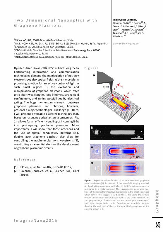
Dye-sensitized solar cells (DSCs) have long been Forthcoming information and communication technologies demand the manipulation of not only electrons but also optical fields at the nanoscale. A promising solution for an active control of light in such small regions is the excitation and manipulation of graphene plasmons, which offer ultra-short wavelengths, long lifetimes, strong field confinement, and tuning possibilities by electrical gating. The huge momentum mismatch between graphene plasmons and photons, however, presents a major technological challenge [1]. Here, I will present a versatile platform technology that, based on resonant optical antenna structures (Fig. 1), allows for an efficient coupling of incoming light into propagating graphene plasmons. More importantly, I will show that these antennas and the use of spatial conductivity patterns (e.g. double layer graphene patches) also allow for controlling the graphene plasmons wavefronts [2], constituting an essential step for the development of graphene plasmonic circuits.
R e f e r e n c e s
[1] J. Chen, et.al. Nature 487, pp77-81 (2012). [2] P.Alonso-González, et. al. Science 344, 1369
(2014).
F i g u r e s
Figure 1: Experimental verification of an antenna-based graphene plasmon device. (A) Illustration of the near-field imaging method. An illuminating plane wave with electric field Ein drives an antenna resonance in a metal nanorod. The subsequently generated near fields at the rod extremities launch plasmons in the graphene sheet, which covers the substrate. A dielectric Si tip scans the sample surface and scatters the local near fields at the sample surface. (B) Topography image of an off- and on-resonance dipole antenna (left and right, respectively). (C,D) Experimental near-field images, showing the real part of the vertical near-field component of the antenna shown in B.
Pablo Alonso-González1,
Alexey Yu Nikitin1,5, F. Golmar1,2, A. Centeno3, A. Pesquera3, S. Vélez1, J. Chen1, F. Koppens4, A. Zurutuza3, F. Casanova1,5, L.E. Hueso1,5, and R. Hillenbrand1,5

I m a g i n e N a n o 2 0 1 5
Gr
ap
he
ne
26
W a f e r - s c a l e f a b r i c a t i o n o f p l a n a r s o l u t i o n - g a t e d g r a p h e n e f i e l d - e f f e c t t r a n s i s t o r s f o r b i o s e n s i n g 1INL – International Iberian Nanotechnology Laboratory, Av. Mestre José Veiga, Braga, Portugal 2CFUM – Centre of Physics of the University of Minho, Campus de Gualtar, Braga, Portugal 3GNano – Nanomedicine and Nanotoxicology Group, Physics Institute of São Carlos, University of São Paulo, São Carlos-SP, Brazil
Recently, graphene has emerged as an alternative material for application in biosensors based on field effect transistors (bio-FET) due to its unique electronic properties combined with its high chemical stability and structural uniformity [1]. Although solution-gated bio-FETs offer interesting advantages compared to other types of biosensors (high sensitivity, label-free detection and large-scale fabrication), the usually large dimensions of gate electrodes (Ag/AgCl reference electrode or a metal wire made of gold, platinum or silver) represent a hindrance for miniaturization of these devices. Since this electrode is essential for gating the transistor it may preclude technological/commercial applications where such systems must work in realistic configurations. Here, we propose the wafer-scale fabrication of solutiongated graphene FETs (SG-GFETs) in which both the metal gate electrode and the transistor array were fabricated in the same wafer. This integration is critical, aiming further applications for bio-sensing, e.g. for advanced point of care testing. Graphene was deposited by CVD from gaseous mixtures of methane, hydrogen and argon on a 25 µm thick copper foil catalyst with 99.999% purity in a quartz tube reactor heated to 1020 °C. It was then transferred to the SiO2/Si wafer final substrate using PMMA as a temporary substrate and dissolving the Cu in a FeCl3 solution. The quality of graphene was assessed using Raman spectroscopy. Fig. 1a shows an optical image of a typical device structure: a 200 mm oxidized silicon wafer was patterned with 280 dies, each comprising three gold contacts: source, drain and a planar gate, with a source-drain gap of 25 µm and the ring-shaped gate at 50 µm around these two
contacts. Several squared pieces of 25 mm of graphene were transferred to cover a large portion of the wafer. Graphene was patterned using optical lithography and oxygen plasma etch keeping the gate Au contact protected by a layer of Al2O3, which is removed later in a wet etch step. The finished set of devices was characterized electrically using 0.01X phosphate buffered saline solution (PBS, pH 7.4) as the gate dielectric. The experiments were carried out by dropping a 20 µL drop of PBS onto the graphene transistor channel. Devices were gated by applying voltage to the integrated gate. A conventional Au wire was also used as gate contact in selected devices for comparison. Fig. 1b shows the transfer curves of the same device gated by conventional gold wire and using the integrated gate. The graphene is unintentionally p-doped which is related to the process and to the substrate. There is a shift in VDirac in the positive axis direction when the device is gated by the integrated gate. The gate-source leakage current is negligible (< 0.03 µA) as compared to the sourcedrain current of the SG-GFET at the same gate potential. Fig. 1c shows normalized transfer curves of eleven devices, obtained by dividing each original curve by the respective ISD maximum. The data show good transistor reproducibility, which is a key requirement for analytical devices. We are currently performing the functionalization of SG-FET channel with specific probes in order to detect disease biomarkers and water toxins. Acknowledgements: G.M.J thanks CNPq for a PhD grant. N.V is thankful to FAPESP for a post-doctoral grant.
N.C.S.Vieira1,3, J. Borme1, G.M. Junior1, M.F. Cerqueira2, P.P. Freitas1, V. Zucolotto3 and P. Alpuim
1,2

I m a g i n e N a n o 2 0 1 5
Gr
ap
he
ne
27
R e f e r e n c e s
[1] Yan, F., Zhang, M., Li, J. Advanced Healthcare
Materials 3 (2014) 313.
F i g u r e s

I m a g i n e N a n o 2 0 1 5
Gr
ap
he
ne
28
N i t r o g e n - d o p e d g r a p h e n e : a t h e o r e t i c a l p o i n t o f v i e w 1Laboratoire d’Etude des Microstructures, ONERA-CNRS, BP 72, 92322 Châtillon Cedex, France 2Physics Department (PMR), University of Namur (FUNDP), B-5000 Namur, Belgium
The introduction of local defects such as vacancies or doping impurities is a well-documented way to tune the electronic properties of graphene. In such a context, nitrogen is a natural substitute for carbon in the honeycomb structure due to both its ability to form sp2 bonds and its pentavalent character. However, a clear correlation between the atomic configuration of the chemically modified graphene and the electronic properties remains a challenging task. Scanning tunneling microscopy and spectroscopy (STM/ STS) are unique tools to measure local electronic properties of graphene and correlate them with their atomic structure [1]. The present work, based on both ab initio DFT, semi-empirical tight-binding (TB) electronic structure calculations and analytical calculations (Green function formalism [2]) aims at looking for interference effects generated by different types of defects. As a first step, the case of simple substitution of nitrogen, where longrange Coulomb effects are expected, will be presented. The Coulomb impurity screening problem in graphene which has been the subject of some debates is discussed [3] and elucidated within a local TB formalism based on the recursion method. This approach is extended to other defects such as vacancy, simple- and double-substitution of nitrogen or pyridine configurations. All the results presented here are discussed in the light of recent experimental STM data [5,6].
R e f e r e n c e s
[1] F. Joucken et al., Phys. Rev. B 85 (2012)
161408(R) [2] F. Ducastelle, Phys. Rev. B 88 (2013) 075413 [3] V.N. Kotov, V.M. Pereira, and B. Uchoa, Phys.
Rev. B 78 (2008) 075433 [4] Ph. Lambin, H. Amara, F. Ducastelle and L.
Henrard, Phys. Rev. B 86 (2012) 045448 [5] Y. Tison et al., (submitted to ACS Nano) [6] T. Mercier, L. Henrard , H. Amara, and F.
Ducastelle (in preparation) F i g u r e s
Figure 1: (a). Map of the local density of states at zero energy in the presence of a vacancy. (b) Local density of states on the nitrogen atom and carbon atoms around a second neighbour nitrogen pair.
H. Amara1,
D. Sharma2, Ph. Lambin2, L. Henrard2, F. Ducastelle1
I m a g i n e N a n o 2 0 1 5
Gr
ap
he
ne
29
G r a p h e n e g r o w t h b y “ m a g i c a l s i z e s ” g r a p h e n e n a n o c l u s t e r s a s s e m b l y o n R e ( 0 0 0 1 ) 1INAC-SPSMS, CEA, 17 rue des Martyrs, F-38054 Grenoble cedex 9, France 2Institut NEEL, CNRS and Université Joseph Fourier, BP166, F-38042 Grenoble Cedex 9, France 2Universite Grenoble Alpes, Inst NEEL, F-38042 Grenoble, France 3CNRS, Inst NEEL, F-38042 Grenoble, France 4SIMAP, Grenoble INP, 1130 rue de la Piscine, BP 75, F-38402 Saint-Martin-d’Hères Cedex, France
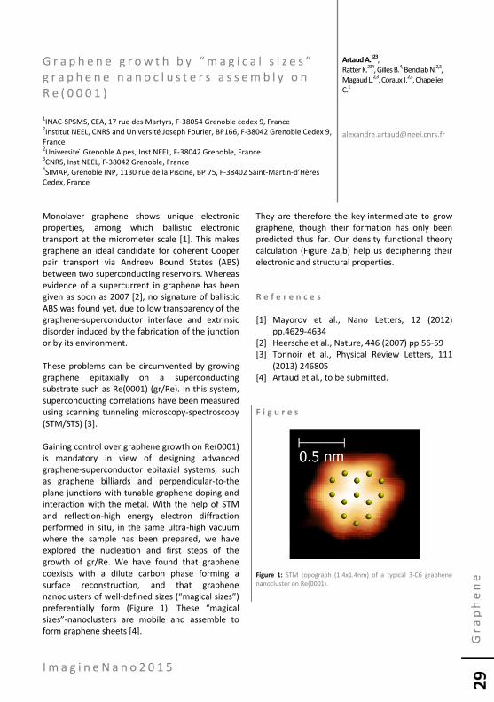
Monolayer graphene shows unique electronic properties, among which ballistic electronic transport at the micrometer scale [1]. This makes graphene an ideal candidate for coherent Cooper pair transport via Andreev Bound States (ABS) between two superconducting reservoirs. Whereas evidence of a supercurrent in graphene has been given as soon as 2007 [2], no signature of ballistic ABS was found yet, due to low transparency of the graphene-superconductor interface and extrinsic disorder induced by the fabrication of the junction or by its environment. These problems can be circumvented by growing graphene epitaxially on a superconducting substrate such as Re(0001) (gr/Re). In this system, superconducting correlations have been measured using scanning tunneling microscopy-spectroscopy (STM/STS) [3]. Gaining control over graphene growth on Re(0001) is mandatory in view of designing advanced graphene-superconductor epitaxial systems, such as graphene billiards and perpendicular-to-the plane junctions with tunable graphene doping and interaction with the metal. With the help of STM and reflection-high energy electron diffraction performed in situ, in the same ultra-high vacuum where the sample has been prepared, we have explored the nucleation and first steps of the growth of gr/Re. We have found that graphene coexists with a dilute carbon phase forming a surface reconstruction, and that graphene nanoclusters of well-defined sizes (“magical sizes”) preferentially form (Figure 1). These “magical sizes”-nanoclusters are mobile and assemble to form graphene sheets [4].
They are therefore the key-intermediate to grow graphene, though their formation has only been predicted thus far. Our density functional theory calculation (Figure 2a,b) help us deciphering their electronic and structural properties.
R e f e r e n c e s
[1] Mayorov et al., Nano Letters, 12 (2012)
pp.4629-4634 [2] Heersche et al., Nature, 446 (2007) pp.56-59 [3] Tonnoir et al., Physical Review Letters, 111
(2013) 246805 [4] Artaud et al., to be submitted. F i g u r e s
Figure 1: STM topograph (1.4x1.4nm) of a typical 3-C6 graphene nanocluster on Re(0001).
Artaud A.123,
Ratter K.234, Gilles B.4, Bendiab N.2,3, Magaud L.2,3, Coraux J.2,3, Chapelier C.1

I m a g i n e N a n o 2 0 1 5
Gr
ap
he
ne
30
Figure 2: DFT-simulated 3-C6 graphene nanocluster on a (7x7) cell of Re(0001). (a) Integrated |ψ|² over the 0 – 0.2 eV range. C atom sizes are proportional to their distance from the Re surface (b) Side-view showing the dome-like shape of the graphene nanocluster..
(a)
I m a g i n e N a n o 2 0 1 5
Gr
ap
he
ne
31
F u t u r e p l a n s f o r E U G r a p h e n e F l a g s h i p EC-Flagships Unit, Belgium
In October 2013 the Commission launched through its FET scheme [1] two FET Flagships, Graphene [2] and the Human Brain Project. Each of them is implemented initially as an FP7 project preparing the ground for what will be a new kind of partnership. FET Flagships are long-term, large scale research initiatives aiming to solve ambitious S&T challenges. They are bringing together excellent research teams across various disciplines, sharing a unifying goal and an ambitious research roadmap to achieve it. In order to address their ambitious objectives Flagships require: (i) Setting up large-scale partnerships that bring together the leading researchers from a large number of research organisations, including academia and industry; (ii) Commitment to a strong science investment over a long time period that cannot be made alone by the European Commission or any single Member State. With Flagships, the Commission proposes a new partnering model for long-term European co-operative research. This model is built around a large Core Project and a number of Partnering
Projects. The Core Project ensures the scientific leadership, continuity and cohesion of the Flagship and is funded by the Commission. The Partnering Projects bring extra knowledge, skills and resources to the Flagship. They may address specific science and technology areas of the Flagship's research roadmap, focus on technology transfer activities, contribute as early users or become early adopters of the Flagships technologies, etc. For each Flagship, the Core Project elaborates a collaboration framework that defines the application procedure, selection
criteria and integration mechanisms of Partnering Projects. Both the Core Project and the Partnering Projects contribute to the management of the Flagship and the definition of its research roadmap. The implementation model of the Graphene Flagship will be presented; it is described in the Commission Staff Working Document on FET Flagships [3].
R e f e r e n c e s
[1] FET, Future and Emerging Technologies, is
the Commission’s scheme that was supporting long-term ICT programmes in FP7 and is now in the Excellence Science part of Horizon 2020.
[2] www.graphene-flagship.eu [3] SWD(2014) 283 final of 16.09. 2014
F i g u r e s
Jean-Marie Auger
I m a g i n e N a n o 2 0 1 5
Gr
ap
he
ne
32
R o b u s t f a b r i c a t i o n o f s u s p e n d e d s t r u c t u r e s f r o m C V D g r a p h e n e 1IMEP-LAHC, Grenoble INP, Minatec, CS 50257, 38016 Grenoble, France 2CRANN Trinity College, Dublin 2, Ireland 3SPSMS, CEA-INAC, 17 rue des Martyrs, 38054 Grenoble Cedex 9, France 4LNCMI, CNRS-UJF-INSA-UPS, 38042 Grenoble Cedex 9, France
Suspended graphene is interesting for nanoelectromechanical systems (NEMS) due to its high stiffness combined with low mass [1] and RF applications due to the increased electrical mobility. [2] For suspended as well as supported devices, it is important to have a large-scale fabrication route. We developed a robust and scale fabrication route for suspended devices from CVD graphene towards industrial applications. By taking particular care of the etching mask/graphene interface, we repeatedly achieved fully self-supported graphene beams in all of the 14 devices on each sample but one or two. A representative SEM image can be observed as in Figure 1a. In addition, we saw that it is possible to suspend more complicated geometries as in Figure 1b which are intended for more elaborate electrical measurements including the extraction of Hall mobility and elimination of contact resistance in suspended graphene structures. Furthermore, we have seen that it was possible to promote or impede periodic fold formation perpendicular to the beam length that survived heat treatments as well as suspending. Such folds, especially sharp ones are predicted to influence local electronic properties as well as chemical reactivity. [3] Therefore, it is imperative to have control over their formation. Compressive strain is a result of the high temperatures of the CVD process in company with the negative thermal expansion coefficient of graphene. While this is partially relaxed into systematic and/or randomly distributed folds, Raman spectroscopy showed that the compression is, in fact, not fully relaxed even at the final step of fabrication. Our
preliminary electrical measurements on graphene devices on SiO2 showed promising contact resistance and Hall mobility. Our care of the interface resulted in contact resistivity values of ~ 2 – 3 Ω µm which is on the lower end of the published values for Cr/Au metals. [4] We calculated a mobility of ~1200 cm2 V-1 s-1 from Hall measurements where we swept the magnetic fields up to 11 T at 4 K and 20 K. While this value appears low, it agrees with electrical mobility in non-annealed CVD graphene devices.
R e f e r e n c e s
[1] van der Zande et al. Nano Lett., 10 (2010)
4869. [2] Happy et al., 2011 Proceedings of 41st
European Microwave Conference (EuMC 2011), (2011)
[3] Zhang and Arroyo, J. Appl. Phys., 113 (2013) 193501
[4] Nagashio et al., Jpn. J. Appl. Phys. 50, (2011) 070108
F i g u r e s
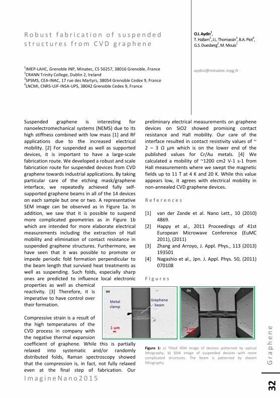
Figure 1: a) Tilted SEM image of devices patterned by optical lithography. b) SEM image of suspended devices with more complicated structures. The beam is patterned by ebeam lithography.
O.I. Aydin1,
T. Hallam2, J.L. Thomassin3, B.A. Piot4, G.S. Duesberg2, M. Mouis1

I m a g i n e N a n o 2 0 1 5
Gr
ap
he
ne
33
T h e e f f e c t o f d e f e c t s p r o d u c e d b y e l e c t r o n i r r a d i a t i o n o n t h e e l e c t r i c a l p r o p e r t i e s o f g r a p h e n e a n d M o S 2 University of Pennsylvania, 209S 33rd St, Philadelphia PA, USA Iramis, CEA Saclay, Gif-sur-Yvette, France
We present a study of the effects of the defects produced by electron irradiation on the electrical and crystalline properties of graphene and MoS2 monolayers. We realized back or side gated electrical devices from monolayer MoS2 or graphene crystals (triangles respectively hexagons) suspended on a 50nm SiNx m. The devices are exposed to electron irradiation inside a 200kV transmission electron microscope (TEM) and we perform in situ conductance measurements [1]. The number of defects and the quality of the crystalline lattice obtained by diffraction are correlated with the observed decrease in mobility and conductivity of the devices. We observe a different behavior between MoS2 and graphene, and try to associate this with different models for conduction with defects. Finally, we use the TEM electron beam to tailor the macroscopic layers into ribbons to be used as the sensing element in MoS2 nanoribbon - nanopore devices for DNA detection and sequencing.
[5] van der Zande et al. Nano Lett., 10 (2010) 4869.
F i g u r e s
Figure 1: a) Schematic representation of the monolayers exposed to the electron beam. b) Increase of resistance of graphene with dose c) Conductance vs gate voltage for pristine and irradiated devices.
Adrian Balan, J. A. Rodriguez- Manzo, M. Puster, P. Masih Das, C. Nayor, A.T.C. Johnson, M. Drndic
I m a g i n e N a n o 2 0 1 5
Gr
ap
he
ne
34
E l e c t r o c h e m i c a l m o d i f i c a t i o n o f g r a p h e n e t o e n h a n c e i t s e l e c t r o n i c a n d v i b r a t i o n a l p r o p e r t i e s 1Max Planck Institute for Solid State Research, Stuttgart (Germany). 2Instituto de Química de São Carlos, Universidade de São Paulo, 13560-970 (Brazil) 3Max Planck Institute for Biophysical Chemistry, 37077 Göttingen (Germany)
Chemical functionalization of graphene allows for a judicious engineering of the physical and chemical properties of graphene. Among the various schemes electrochemical modification [1] presents a versatile and straightforward strategy to fine tune the properties of graphene for a specific application, of which two examples will be presented here. On the one hand it allows us to improve the electronic and electrochemical performance, while on the other it provides us with a handle to continuously tune the extent of Raman scattering. In the first part, we show that trace metal impurities present on graphene have a significant impact on its physical and chemical properties. This observation has recently been made in a number of CVDgrown and graphite-derived graphene samples. This is analogous to the case of carbon nanotubes where trace metals were found to have a strong effect on the electrocatalytic properties of the material. We observe by direct electroanalysis that even after the usual copper etching process, trace copper impurities still remain on transferred CVD graphene. We devise an electrochemical etching procedure [2] using which we successfully eliminate at least 90% of these impurities with a clear improvement in both the electrochemical and electronic transport properties of monolayer graphene. In the second part we present an electrochemical deposition route to attach gold nanoparticles (AuNPs) controllably on to a graphene surface. Raman scattering in graphene can be significantly enhanced through the coupling of metal nanostructures. Many of the reported approaches utilize physical vapor depositon requiring
patterning of graphene or the underlying substrate. A major limitation is the inability to measure the Raman enhancement at the same location as a function of variation in particle size and / or density. Moreover, there is no direct possibility to tune the strength of enhancement after the structures are fabricated. Using our electrodeposition route, the size or density of the nanoparticles and thereby the Raman enhancement can be continuously increased through appropriate choice of electrochemical parameters. [3] We clearly show that the strength of Raman enhancement varies as a function of the frequency of the vibrational mode (D, G or 2D of graphene) and may be correlated with the plasmonic fingerprint of the attached AuNPs. An additional chemical contribution can be also deciphered through charge transfer from AuNPs on to graphene. Subsequently, we show that these devices can be efficiently utilized as SERS substrates for the detection of specifically bound non-resonant analyte molecules.
R e f e r e n c e s
[1] R.S. Sundaram, et al., Adv. Mater. 20, 3050
(2008). [2] R.M. Iost et al., ChemElectroChem Early View
DOI: 10.1002/celc.201402325 [3] L. Zuccaro, et al., Adv. Funct. Mater. 24, 6348
(2014).
Kannan Balasubramanian1,
L. Zuccaro1, R.M. Iost1,2, F.N. Crespilho2, H.K. Yu3, A.M. Wodtke3, K. Kern1

I m a g i n e N a n o 2 0 1 5
Gr
ap
he
ne
35
S p i n d i f f u s i o n l e n g t h i n L S M O –g r a p h e n e s p i n v a l v e s 1Cambridge Graphene Centre, University of Cambridge, CB3 0FA, Cambridge, UK 2Department of Materials Science & Metallurgy, University of Cambridge, Cambridge, UK 3Department of Applied Physics, Aalto University School of Science, FI-00076, Aalto Finland 4Department of Physics, University of Parma, 43100, Parma, Italy 5Diamond Light Source, Chilton, Didcot, OX11 0DE UK
Significant progress has been made in graphene spintronics since the first demonstration of a graphene-based spin valve [1]. Due to low spin-orbit coupling [2] and hyperfine interaction [2], spin diffusion lengths have been measured in the range from 1.5 µm [3] up to 285 µm [4]. Here we present spin valves formed by combining La2/3Sr1/3MnO3 (LSMO) electrodes and few layer graphene channels. LSMO exhibits interfacial spin-polarization close to 100% at low temperature [5], making it a promising material for spin valves with highly spin-polarized electrodes [6]. We report spin transport on a device fabricated combining a 5 layer graphene and LSMO. The electrodes show a 20% X-ray magnetic circular dichroism contrast (XMCD) asymmetry at remanence after magnetic pulses, as confirmed by photoemission electron microscopy with XMCD. The transition between parallel and anti-parallel states occurs at distinct and well defined magnetic fields. This is further confirmed by magneto-optic Kerr effect microscopy. The resistance difference between the antiparallel and parallel configurations is ΔR=1.0 MΩ, corresponding to a magnetoresistance of 5.5% at 10 K (Fig. 1), and a spin diffusion length~100 μm (Fig.2). Importantly, our analysis excludes the contribution from tunnelling anisotropic magnetoresistance (TAMR), and allows us to attribute the recorded magnetoresistance entirely to spin transport.
R e f e r e n c e s
[1] E.W. Hill et al., IEEE Trans. Magn. 42 (2006)
2694. [2] D. Huertas-Hernando et al., Pys. Rev. B 74
(2006) 155426. [3] N. Tombros et al., Nature. 448 (2007) 571. [4] B. Dlubak et al., Nat. Phys. 8 (2012) 557.
[5] M.Bowen et al., Appl. Phys. Lett. 82 (2003) 233.
[6] L. Hueso et al., Nature 445 (2007) 410.
F i g u r e s
Figure 1: Magneto-transport measurements on a 5-layer graphene on LSMO electrodes. Blue and black line correspond to the directions of magnetic field sweep indicated by the arrows.
Figure 2: Simulated magnetoresistance (MR) as a function of interfacial spin polarisation γ, spin diffusion length lsf, and interfacial resistance rb
* using the drift-diffusion model. The blue line indicates the range of values derived for our device.
M. Barbone1,
W. Yan2, L. C. Phillips2, S. Hämäläinen3, A. Lombardo1, M. Ghidini2,4, X. Moya2, F. Maccherozzi5, S. van Dijken3, S. S. Dhesi5, N. D. Mathur2 and A. C. Ferrari1

I m a g i n e N a n o 2 0 1 5
Gr
ap
he
ne
36
E x c e p t i o n a l b a l l i s t i c t r a n s p o r t i n s e l f -a s s e m b l e d s i d e w a l l g r a p h e n e n a n o r i b b o n s 1Leibniz Universität Hannover, Institut für Festkörperphysik, 30167 Hannover, Germany 2Georgia Institute of Technology, Atlanta, Georgia 30332-0430, USA
The patterning of graphene into graphene nanoribbons is an essential task for the development of future graphene based electronic devices. For such ribbons with a well-ordered edge geometry the presence of one-dimensional edge states has been predicted. We use a selective graphitization process on the sidewalls of SiC mesa structures to produce graphene nanoribbons with a width of 40 nm. The local electronic properties of the ribbons are investigated by means of a 4-tip scanning tunneling microscope (STM). In combination with a high-resolution scanning electron microscope (SEM), the precise positioning of all four tips on the nanometer range is possible to perform local transport measurements [1] (cf. Fig. 1(a)). Additionally, one of the STM tips can be used for scanning tunneling spectroscopy (STS) to gain an insight into the local density of states. The STS reveals two peaks in the local density of states at the edges of the ribbons which can be attributed to the zeroth subbands in the band structure of a ferromagnetic zig-zag graphene nanoribbon [2]. Transport experiments carried out on the very same ribbon show a conductance close to e2/h for a wide temperature range from 30 K up to room temperature and probe spacings between 1 µm and 10 µm. Description within the Landauer formalism is possible assuming ballistic transport dominated by a single channel. Transport in the second zeroth subband is only detectable for probe spacings smaller than 1 µm due to the short localization length of carriers in this subband. This manifests in the increase of the conductance to 2 e2/h at probe spacings below 200 nm (cf. Fig. 1(b)). As a consequence, it is possible to selectively measure transport in one or two ballistic channels. Remarkably, 4-point probe and 2-point probe configurations result in almost identical conductance values as expected for a ballistic
conductor measured with fully invasive probes. This invasiveness of the probes can be used to give further evidence for the ballistic nature of transport, simply by introducing one or two additional passive probes in a 2-point probe configuration. Every additional passive probe doubles or triples the observed resistance, a clear indication for single-channel ballistic transport [3]..
R e f e r e n c e s
[1] J. Baringhaus et al., Appl. Phys. Lett., 103
(2013) 111604. [2] J. Baringhaus et al., J. Phys.: Condens. Matter,
25 (2013) 392001. [3] J. Baringhaus et al., Nature, 506 (2014) 349.
F i g u r e s
Figure 1: (a) SEM image of four probes contacting a sidewall graphene nanoribbon. (b) Conductance as a function of probe spacing of a sidewall graphene nanoribbon.
Jens Baringhaus1,
Claire Berger2, Walt de Heer2, and Christoph Tegenkamp1

I m a g i n e N a n o 2 0 1 5
Gr
ap
he
ne
37
A n o m a l o u s H a l l E f f e c t i n f e r r o m a g n e t i c g r a p h e n e University of California at Riverside, Department of Physics and Astronomy, Riverside, USA
Recent advancements in device transfer techniques have enabled transfer of graphene on ferromagnetic substrates, which leads to a proximity induced ferromagnetism of the graphene sheet [1]. The presence of ferromagnetic exchange along with Rashba spin-orbit coupling leads to an energy gap at the Dirac points [2]. When the Fermi energy is pinned in the gap this system exhibits a quantized anomalous Hall with Chern number 2. I will show that when the Fermi energy is not in the gap the system exhibits un-quantized anomalous Hall effect (AHE) due to an intrinsic (band structure effect) and an extrinsic (disorder induced effect) contribution. The AHE contributions due to the intrinsic and extrinsic mechanisms will be calculated in semi-classical Boltzmann transport. The ability to gate tune the two-dimensional carrier density of the graphene sheet allows for a more detailed study of the anomalous Hall than that previously available in ferromagnetic semi-conductors. I will compare our theoretical results with most recent experimental data.
R e f e r e n c e s
[1] Zhiyong Wang, Chi Tang, Raymond Sachs,
Yafis Barlas, Jing Shi, Proximity-induced ferromagnetism in graphene revealed by anomalous Hall effect, cond-mat/1412.1521 (to be published in PRL).
[2] Z. Qiao, H. Jiang, X. Li, Y. Yao and Q. Niu, Phys. Rev. B 85, 115439 (2012)..
Yafis Barla, Jing Shi, Roger Lake
I m a g i n e N a n o 2 0 1 5
Gr
ap
he
ne
38
S e n s i n g c a p a b i l i t i e s o f a s i n g l e - l a y e r M o S 2 s u b s t r a t e f o r m o l e c u l e d e t e c t i o n 1Dpto. Electrónica y Tecnología de Computadores, Universidad de Granada, 18071, Granada, Spain 2Dpto. Física Teórica de la Materia Condensada, Universidad Autónoma de Madrid, 28049, Madrid, Spain
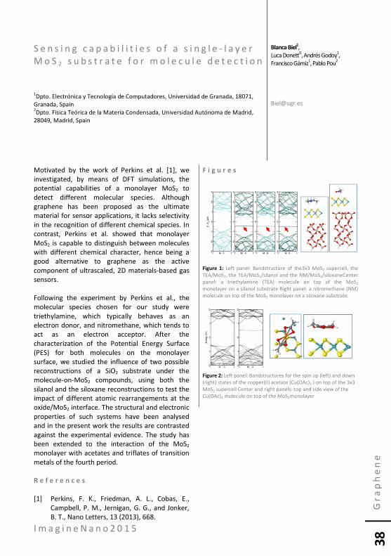
Motivated by the work of Perkins et al. [1], we investigated, by means of DFT simulations, the potential capabilities of a monolayer MoS2 to detect different molecular species. Although graphene has been proposed as the ultimate material for sensor applications, it lacks selectivity in the recognition of different chemical species. In contrast, Perkins et al. showed that monolayer MoS2 is capable to distinguish between molecules with different chemical character, hence being a good alternative to graphene as the active component of ultrascaled, 2D materials-based gas sensors. Following the experiment by Perkins et al., the molecular species chosen for our study were triethylamine, which typically behaves as an electron donor, and nitromethane, which tends to act as an electron acceptor. After the characterization of the Potential Energy Surface (PES) for both molecules on the monolayer surface, we studied the influence of two possible reconstructions of a SiO2 substrate under the molecule-on-MoS2 compounds, using both the silanol and the siloxane reconstructions to test the impact of different atomic rearrangements at the oxide/MoS2 interface. The structural and electronic properties of such systems have been analysed and in the present work the results are contrasted against the experimental evidence. The study has been extended to the interaction of the MoS2 monolayer with acetates and triflates of transition metals of the fourth period.
R e f e r e n c e s
[1] Perkins, F. K., Friedman, A. L., Cobas, E.,
Campbell, P. M., Jernigan, G. G., and Jonker, B. T., Nano Letters, 13 (2013), 668.
F i g u r e s
Figure 1: Left panel: Bandstructure of the3x3 MoS2 supercell, the TEA/MoS2, the TEA/MoS2/silanol and the NM/MoS2/siloxaneCenter panel: a triethylamine (TEA) molecule on top of the MoS2 monolayer on a silanol substrate Right panel: a nitromethane (NM) molecule on top of the MoS2 monolayer on a siloxane substrate.
Figure 2: Left panel: Bandstructures for the spin up (left) and down (right) states of the copper(II) acetate (Cu(OAc)2 ) on top of the 3x3 MoS2 supercell Center and right panels: top and side view of the Cu(OAc)2 molecule on top of the MoS2monolayer
Blanca Biel1,
Luca Donetti1, Andrés Godoy1, Francisco Gámiz1, Pablo Pou2

I m a g i n e N a n o 2 0 1 5
Gr
ap
he
ne
39
E n e r g y c o n v e r s i o n a n d s t o r a g e d e v i c e s b a s e d o n s o l u t i o n p r o c e s s e d 2 d c r y s t a l s Istituto Italiano di Tecnologia, Graphene Labs, Via Morego 30, 16163 Genova, Italy
Energy conversion and storage are two of the grand challenges that our society is currently facing. New materials and processes [1] can improve the performance of existing devices or enable new ones [1-5] that are also environmentally friendly. In this context, graphene and other two-dimensional (2d) crystals are emerging as promising materials. [1-5] A key requirement for energy conversion and storage applications is the development of industrial-scale, reliable, inexpensive production processes, [2] while providing a balance between ease of fabrication and final material quality with on-demand properties. [2] Solution-processing [2,6] is offering a simple and cost-effective pathway to fabricate various 2d crystal-based energy devices, presenting huge integration flexibility compared to conventional methods. Here I will present an overview of graphene and other 2d crystals-based energy conversion and storage applications, starting from solution processing of the raw bulk materials, [2,7,8] the fabrication of large area electrodes [3] and their integration in lithium-ion batteries [8,9] and photovoltaic devices. [10]
R e f e r e n c e s
[1] A. C. Ferrari, F. Bonaccorso, et al., Scientific
and technological roadmap for graphene, related two-dimensional crystals, and hybrid systems. Nanoscale DOI: 10.1039/c4nr01600a (2014).
[2] F. Bonaccorso, et al., Production and processing of graphene and 2d crystals. Materials Today, 15, 564-589, (2012).
[3] F. Bonaccorso, et. al., Graphene photonics and optoelectronics. Nature Photonics 4, 611-622,(2010).
[4] F. Bonaccorso, Z. Sun, Solution processing of graphene, topological insulators and other 2d crystals for ultrafast photonics. Opt. Mater. Express 4, 63-78 (2014).
[5] G. Fiori, et al., Electronics based on two-dimensional materials. Nature Nanotech 9, , 768-779, (2014).
[6] Y. Hernandez, et al., High-yield production of graphene by liquid-phase exfoliation of graphite. Nature Nanotech 3, 563-568, (2008).
[7] O. M. Maragò, et al., Brownian motion of graphene. ACS Nano, 4, 7515-7523 (2010).
[8] J. Hassoun, et al. An advanced lithium-ion battery based on a graphene anode and a lithium iron phosphate cathode Nano Lett. 14, 4901-4906 (2014).
[9] F. Bonaccorso, et. al., Graphene, related two-dimensional crystals, and hybrid systems for energy conversion and storage. Science, 347, 1246501 (2015).
[10] P. Robaeys, et al. Enhanced performance of polymer: fullerene bulk heterojunction solar cells upon graphene addition. Appl. Phys. Lett. 105, 083306 (2014).
Francesco Bonaccorso

I m a g i n e N a n o 2 0 1 5
Gr
ap
he
ne
40
S c i e n c e a n d t e c h n o l o g y o f t w o -d i m e n s i o n a l c r y s t a l s @ I s t i t u t o I t a l i a n o d i T e c n o l o g i a , G r a p h e n e L a b s Istituto Italiano di Tecnologia, Graphene Labs, Via Morego 30, 16163 Genova, Italy
The Italian Institute of Technology (IIT) is a Foundation established in 2003 jointly by the Italian Ministry of Education, University and Research and the Ministry of Economy and Finance to promote excellence in basic and applied research. The research plan of the institute focuses on Humanoid technologies and Robotics, Neuroscience and Cognition, Nanotechnology and Materials. The Institute has a staff of about 1300 people, the central research lab being located in Genoa. IIT has a large experience with the management of large research projects and has been involved in more than 100 EU funded projects in the last 8 years. IIT headquarter in Genoa has a 30,000m2 facility equipped with state-of-the-art laboratories for robotics, nanoscience and neuroscience, and 10 Research Centres all over the country. Since September 2013 IIT graphene research is collected under the umbrella of the IIT Graphene Labs (http://graphene.iit.it), which currently involves more than 30 researchers working on different aspects of graphene and 2d crystals science and technology. IIT Graphene Labs is actively involved in realising scientific and technological targets in the field of energy conversion [1,2] and storage [3] , material production (e.g., CVD [4] and solution processing [3]), deposition [5] and composite production [6], as well as heterostructures [7] and bio-nanotechnology (e.g., biocompatibility essays, biomolecule-graphene interaction). We will also have a strong effort in dissemination and technology transfer activities. In particular, the technology transfer program of IIT Graphene Labs is developing through specific agreements with companies. At the moment we have in place agreements with more than 10 companies on different aspects of graphene technology. The relevant facilities available span from colloidal
chemistry synthesis for nanoparticle production, electron microscopies, low temperature scanning tunnelling microscopies, optical spectroscopies from femtosecond to continues wave, a class 100 clean room for nanofabrication (600m2) and finally a the processing and prototypes unit, equipped with state-of-the-art 2d crystals production and coating instruments.
R e f e r e n c e s
[1] F. Bonaccorso, et al., Science 347, 1246501,
2015. [2] G. Calogero, et al., Chem. Soc. Rev. DOI:
10.1039/c4cs00309h, 2015. [3] J. Hassoun, et al., Nano Lett. 14, 4901-4906,
2014. [4] V. Miseikis, et al., 2D Materials 2, 014006,
2015. [5] G. Fiori, et al., Nature Nanotech. 9, 768-779,
2014. [6] E. Jomehzadeh, et al., Comput. Mat. Sci. 99,
164-172, 2015. [7] A. Gamucci, et al., Nature Comm. 5, 5184,
2014.
Francesco Bonaccorso
and Vittorio Pellegrini
I m a g i n e N a n o 2 0 1 5
Gr
ap
he
ne
41
G r a p h e n e b a s e d e l e c t r o d e s f o r h i g h p e r f o r m a n c e s s u p e r c a p a c i t o r s Head of the nanomaterial topic team, Joint unit CNRS/Thales, Physics Department Thales Research and Technology, 91120 Palaiseau, France
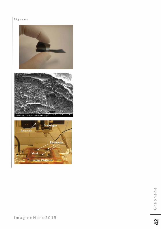
Supercapacitors are electrochemical energy storage devices that combine the high energy-storage-capability of conventional batteries with the high power-delivery-capability of conventional capacitors. In this contribution we will show the results of our group recently obtained on supercapacitors with electrodes obtained using mixtures of carbonaceous nanomaterials (carbon nanotubes (CNTs), graphite, graphene, oxidised graphene). The electrode fabrication has been performed using a new dynamic spray-gun based deposition process set-up at Thales Research and Technology (patented). This technique constitute a real breakthrough compared to the classical filtration method because electrodes can be deposited over large areas in a completely automated way, using different kinds of substrates and with a thickness between some nm and up to hundredth of μms. In a first step, we will show the properties of mixtures of graphite/CNTs as a function of their composition (%) and of their weight for the fabrication of electrodes and cells. In order to spray the nanomaterials on a substrate we put them in stable suspensions using specific solvents. In case of CNTs/Graphite we used N-Methyl-Pyrrolidone. To avoid the “coffee-ring” effect” we have to heat the substrate and to reach the boiling point of the solvent (~220°C for NMP). The supercapacitor electrodes were fabricated on low cost graphite current collectors (commercially available) which are flexible and highly conducting. First, we systematically studied the effect of the relative concentrations of CNTs and graphite on the energy and power density. We obtained a power increase of a factor 2.5 compared to barely CNTs based electrodes for a mixture composed by 75% of graphite. After these results, we decided to test water as a solvent in order to reduce the
heating temperature and to obtain a green type process without toxic solvents. To achieve stable suspensions we oxidised the graphene and the CNTs before putting them in water. In this way we were able to fabricate stable suspensions in less than one hour compared to three days using NMP. Finally we will show recent results obtained using graphene exfoliated by IIT, that allows us improving the power of the supercapacitors in a dramatic way, thanks to its high conductivity. All these results demonstrate the strong potential to obtaining high performance devices using an industrially suitable fabrication technique.
R e f e r e n c e s
[1] Supercapacitor electrode based on mixtures
of graphite and carbon nanotubes deposited using a new dynamic air-brush deposition technique, P Bondavalli, C.Delfaure, P.Legagneux, D.Pribat JECS 160 (4) A1-A6, 2013
[2] Non-faradic carbon nanotubes based supercapacitors : state of the art, P.Bondavalli, D.Pribat, C.Delfaure, P.Legagneux, L.Baraton, L.Gorintin, J-P. Schnell, Eur. Phys. J. Appl. Phys. 60,10401, 2012.
Paolo Bondavalli
I m a g i n e N a n o 2 0 1 5
Gr
ap
he
ne
42
F i g u r e s

I m a g i n e N a n o 2 0 1 5
Gr
ap
he
ne
43
L a b - s c a l e s y s t e m f o r a u t o m a t e d g r a p h e n e t r a n s f e r 1Inst. de Sistemas Optoelectrónicos y Microtecnología, UPM, Madrid, 28040, Spain 2Dpto. de Ingeniería Electrónica, E.T.S.I de Telecomunicación, UPM, Madrid, 28040, Spain 3Campus de Excelencia Internacional, Campus Moncloa UCM-UPM, Madrid, 28040, Spain 4Dpto. de Ciencia de Materiales, E.T.S.I de Caminos, Canales y Puertos, UPM, Madrid, 28040, Spain
Although chemical vapor deposition (CVD) has proven to be an excellent method for growing electronic-quality graphene, its main disadvantage is the need of transferring the graphene layer from the metal catalyst to a suitable final substrate. A manual transfer method [1] was developed to overcome this issue. It consists of protecting the graphene with a thin polymer layer, wet-etching the growth substrate, rinsing with deionized water, and finally depositing the resulting polymer/graphene membrane onto the desired target substrate. Despite this method has been strongly optimized [2,3], it still requires strong handling skills, is time consuming, and is not suitable for an industrial process. An alternative method based on a roll-to-roll system [4] can overcome some limitations of the manual method, but it is limited to flexible substrates. In this work we report on a lab-scale system designed to transfer graphene automatically to arbitrary substrates, which could be easily scaled up for industrial applications. The system is composed of several modules (Fig. 1) that control the process temperature, the liquid flow and the overall system state. An Arduino UNO microcontroller is used as the real-time control system, timing and activating the rest of modules. It also allows communication with a computer for logging purposes. The passive components of the system are depicted in Fig. 2. A polytetrafluoroethylene (PTFE) tube encloses the graphene sample during the whole process. This enclosing tube has a surface treatment that centers the polymer/graphene membrane that floats inside it. The treatment avoids mechanical stress or induced ripples in the graphene during the process. A fixed platform and a substrate holder ensure a fixed position between the final substrate and the tube center. All these pieces are
immersed into a liquid, starting with an etchant solution and changing gradually into deionized water for the final rinsing steps. Finally, graphene field-effect transistors (GFETs) were processed on the same CVD material but transferred using both the standard manual method and the novel automatic method for comparison. Raman and electrical assessment of the GFETs demonstrate that devices on the automatically-transferred graphene present systematically higher mobilities and less impurity contamination.
Acknowledgements: Supported by MINECO projects RUE (CSD2009-0046) and GRAFAGEN (ENE2013-47904-C3).
R e f e r e n c e s
[1] Alfonso Reina, Xiaoting Jia, et al., Nano Lett.,
vol. 9, 1 (2009), p. 30. [2] Wei-Hsiang Lin, Ting-Hui Chen, et al., ACS
Nano, vol. 8, 2 (2014), p. 1784. [3] Hai Li, Jumiati Wu, et al., ACS Nano, vol. 8, 7
(2014), p. 6563. [4] Sukang Bae, Hyeongkeun Ri Kim, et al., Nat.
Nanotechnol., vol. 5, August (2010), p. 1.
Alberto Boscá1, 2,
J. Pedrós1, 3, J. Martínez1, 4, F. Calle1, 2, 3

I m a g i n e N a n o 2 0 1 5
Gr
ap
he
ne
44
F i g u r e s
Figure 1: System modules. An Arduino UNO board is used for interconnection and control.
Figure 2: Figure 2: PTFE passive components (in liquid) and the sample and final substrate.

I m a g i n e N a n o 2 0 1 5
Gr
ap
he
ne
45
C o r r e l a t i n g e l e c t r i c a l m e a s u r e m e n t s o f c a r b o n n a n o s t r u c t u r e s i n s i d e t h e T E M w i t h f i r s t p r i n c i p l e s c a l c u l a t i o n s 1IMCN-NAPS Université catholique de Louvain, Chemin des étoiles 8, 1348 Louvain la neuve, Belgium 2Institut de Physique et Chimie des Matériaux de Strasbourg, UMR 7504 CNRS, University of Strasbourg, 23 rue du Loess, 67034 Strasbourg 3Department of Physics and Astronomy, University of Pennsylvania, Philadelphia, Pennsylvania 19104, USA.
The interest of carbon nanostructues as potential active or passive components in next generation electronics is in great part due to the large range of properties that these systems exhibit. For instance, it has been shown theoretically that the electronic structure of carbon nanotubes (CNTs) and carbon nanoribbons (CNRs) strongly depend on the details of their atomic structure. This represents both an opportunity to tailor the electrical properties and a challenge to achieve atomically precise synthesis and characterization. In particular, the electrical characterization of carbon nanostructures has been elusive due to the challenging task of having accurate information of both the atomic structure and the electrical response. Recent breakthroughs in the spatial resolution of electron microscopes and the possibility to make electrical measurements inside them have provided unprecedented information about the electrical behaviour of these systems. Coupled with simulations, important contributions to the understanding of the electrical behaviour of carbon nanostructures have been made. Here, the specific examples of the electronic characterization of atomic chains of carbon and CNRs are used to compare with transport calculations based on first-principles DFT and tight biniding models [1-3]. The qualitative agreement between experiment and simulation allow a solid understanding of the properties of these systems. However, the quantitative discrepancies offer challenges on both sides.
R e f e r e n c e s
[1] O. Cretu, A.R. Botello-Mendez, I. Janowska, C.
Pham-Huu, J.-C. Charlier, F. Banhart, Nano Lett. 13 (2013) 3487.
[2] Z.J. Qi, J.A. Rodríguez-Manzo, A.R. Botello-Méndez, S.J. Hong, E.A. Stach, Y.W. Park, J.-C. Charlier, M. Drndić, A.T.C. Johnson, Nano Lett. 14 (2014) 4238.
[3] A. La Torre, A.R. Botello-Mendez, J.-C. Charlier, F. Banhart, Nature Comm. (2014) submitted.
F i g u r e s
Figure 1: Schematic view of the transport through a carbon chain inside the TEM.
Andrés R. Botello-Méndez1,
O. Cretu2, A. La Torre2, Z. J. Qi3, J. A. Rodríguez-Manzo3, M. Drndic3, A.T. C. Johnson3, F. Banhart2, J.-C. Charlier1

I m a g i n e N a n o 2 0 1 5
Gr
ap
he
ne
46
T h e G r a p h e n e F l a g s h i p Graphene Flagship, Sweden
The Graphene Flagship is a ten-year research program funded by the European Commission, EU member states and project participants. It originates from the science of graphene and related layered materials and targets a disruptive technology shift, bringing these materials from academic laboratories to society as new products, employment opportunities and economic growth. Realising this ambition is only possible by integrating the entire value chain from basic research to applied and industrial research, which requires a large consortium with corresponding resources – the total project cost is about one billion euros. The flagship covers a wide range of topics ranging from fundamental research and spintronics to flexible electronics and nanocomposites. Examples of research carried out in some of the work packages will be briefly presented, but technical details cannot be covered, in the interest of time. Ways of interacting with the Graphene Flagship will be described, as well as the planned development of the Flagship during Horizon 2020.
Katarina Boustedt
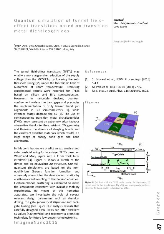
I m a g i n e N a n o 2 0 1 5
Gr
ap
he
ne
47
Q u a n t u m s i m u l a t i o n o f t u n n e l f i e l d -e f f e c t t r a n s i s t o r s b a s e d o n t r a n s i t i o n m e t a l d i c h a l c o g e n i d e s 1IMEP-LAHC, Univ. Grenoble Alpes, CNRS, F-38016 Grenoble, France 2DIEG-IUNET, Via delle Scienze 208, 33100 Udine, Italy
The tunnel field-effect transistors (TFETs) may enable a more aggressive reduction of the supply voltage than the MOSFETs, by lowering the sub-threshold swing (SS) under the thermionic limit of 60mV/dec at room temperature. Promising experimental results were reported for TFETs based on silicon and III-V semiconductors. However, in nanoscale devices, quantum confinement widens the band gaps and precludes the implementation of truly broken band gap alignments in 3D semiconductors [1], while interface states degrade the SS [2]. The use of semiconducting transition metal dichalcogenides (TMDs) may represent an extremely advantageous alternative thanks to their intrinsic 2D geometry and thinness, the absence of dangling bonds, and the variety of available materials, which results in a large range of energy band gaps and band alignments. In this contribution, we predict an extremely steep sub-threshold swing for inter-layer TFETs based on WTe2 and MoS2 layers with a 1 nm thick h-BN interlayer [3]. Figure 1 shows a sketch of the device and its equivalent 2D structure. Our full-quantum simulations are based on the non-equilibrium Green’s function formalism and accurately account for the device electrostatics by a self-consistent coupling to the Poisson equation. Electron-phonon scattering is calibrated to make the simulations consistent with available mobility experiments. By means of this numerical apparatus, we investigate the role of several relevant design parameters such as chemical doping, top gate geometrical alignment and back-gate biasing (see Fig.2). Our analysis reveals that carefully designed TMD TFETs can offer excellent SS values (<30 mV/dec) and represent a promising technology for future low-power nanoelectronics.
R e f e r e n c e s
[1] S. Brocard et al., IEDM Proceedings (2013)
5.4.1. [2] M. Pala et al., IEEE TED 60 (2013) 2795. [3] M. Li et al., J. Appl. Phys. 115 (2014) 074508.
F i g u r e s
Figure 1: (a) Sketch of the TFET under study. (b) Equivalent 2D model used in the simulations. The x2D axis corresponds to the y-direction for MoS2 and to x-direction for WTe2.
Jiang Cao1,
Marco Pala1, Alessandro Cresti1 and David Esseni2
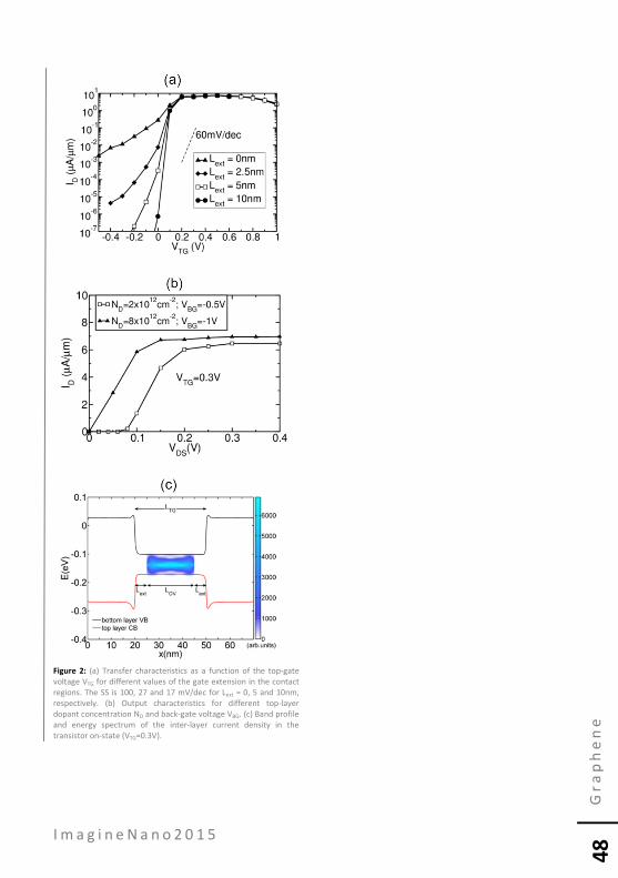
I m a g i n e N a n o 2 0 1 5
Gr
ap
he
ne
48
Figure 2: (a) Transfer characteristics as a function of the top-gate voltage VTG for different values of the gate extension in the contact regions. The SS is 100, 27 and 17 mV/dec for Lext = 0, 5 and 10nm, respectively. (b) Output characteristics for different top-layer dopant concentration ND and back-gate voltage VBG. (c) Band profile and energy spectrum of the inter-layer current density in the transistor on-state (VTG=0.3V).

I m a g i n e N a n o 2 0 1 5
Gr
ap
he
ne
49
M o S 2 T r a n s i s t o r s w i t h E l e c t r o g r a f t e d O r g a n i c U l t r a t h i n F i l m a s E f f i c i e n t G a t e D i e l e c t r i c CEA Saclay, IRAMIS / NIMBE / LICSEN, F-91191 Gif sur Yvette, France
Two dimensional layered semiconductors, and in particular transition metal dichalcogenides such as molybdenum disulfide (MoS2), have recently received increasing attention due to the combination of their unique electronic properties with their atomically thin geometry. Contrary to graphene, MoS2 has a finite band gap of 1.2-1.9 eV (depending on the number of layers), thus complying with the requirements of digital electronic applications. To maximize the potential of MoS2 as channel material in field effect transistors, it must be associated with an efficient gate dielectric. Beside the mainstream CMOS technology, other fields such as large-area and/or printable electronics, sensors and display technologies could also benefit from the combination of 2D materials and new dielectrics, especially if these dielectrics present additional advantages in terms of mechanical flexibility, low temperature processes, conformability to structured substrates, cost and simplicity of equipment and processes, etc. In this respect, the development of robust organic nano-dielectrics and their combination with new semiconductors represent a high potential route. In this context, we developed new dielectrics based on electrografted organic thin films on metallic electrodes. These dielectrics are produced at room temperature and under mild conditions. The process yields uniform films of nanometer thickness (4-8 nm range). In this work [1], we demonstrated the first transistors combining MoS2 as channel material and an electrografted organic ultrathin film as gate dielectric. The transistors exhibit high ION/IOFF ratio together with steep subthreshold slope as low as 110 mV/decade. Besides, the transfer characteristics of these transistors have no-hysteresis due to the
hydrophobic and trap-free nature of our electrografted dielectric. The transistors reported in [1] were fabricated on rigid substrates and using mechanically exfoliated MoS2. Their potential in large scale (based on CVD MoS2) and flexible electronics will be discussed on the basis of our latest results.
R e f e r e n c e s
[1] H. Casademont, L. Fillaud, X. Lefèvre, B.
Jousselme, V. Derycke, submitted. F i g u r e s
Hugo Casademont,
Laure Fillaud, Xavier Lefevre, Renaud Cornut, Bruno Jousselme, Vincent Derycke

I m a g i n e N a n o 2 0 1 5
Gr
ap
he
ne
50
F r o m G r a p h e n e t o P h o s p h e r e n e : t h e 2 D z o o Centre for Advanced 2D Materials and Graphene Research Centre National University of Singapore 6 Science Drive 2, Singapore 117546
The field of two dimensional materials is rapidly expanding with the isolation and synthesis of many atomically thin crystals that present a broad variety of physical and chemical properties which can be exploited in different areas of science and engineering. In this talk I will review the progress in this exciting new area of research.
Antonio H. Castro Neto

I m a g i n e N a n o 2 0 1 5
Gr
ap
he
ne
51
H o l e M o b i l i t y E n h a n c e m e n t a n d p -d o p i n g i n M o n o l a y e r W S e 2 b y G o l d D e c o r a t i o n 1Center for Micro/Nano Science and Technology, National Cheng Kung Uni., Tainan, Taiwan 2Institute of Atomic and Molecular Sciences, Academia Sinica, Taipei, 11529, Taiwan 3Department of Applied Physics, Waseda University, Tokyo 169-8555, Japan 4Physical Sciences and Engineering, King Abdullah University of Science and Technology, Thuwal, 23955-6900, Kingdom of Saudi Arabia
Tungsten diselenide (WSe2) is an attractive transition metal dichalcogenide material, since its Fermi energy close to the mid gap makes it an excellent candidate for realizing p–n junction devices and complementary digital logic applications. Doping is one of the most important technologies for controlling the Fermi energy in semiconductors, including 2D materials. Moreover, the Fermi level engineering or doping in monolayer WSe2 is still relatively unexplored. Recently, Fang et al have reported transistors based on WSe2 using high-k materials as the gate dielectrics, where the chemically doped source/drain contacts exhibit low contact resistances. Selective treatment with potassium is able to form degenerately doped n+ contacts for electron injection while NO2 treatment forms p+ contacts [1–3]. Liu et al have demonstrated the n-type WSe2 FET by using indium as a contact metal [4]. Chuang et al have revealed that graphene can be a work-function-tunable electrode material for few-nanometre WSe2 FETs [5]. It is noted that the small molecules adsorbed on the 2D materials tend to desorb from the surfaces and the alkali metals are known to be sensitive to moisture and oxygen. Here we present a simple, stable and controllable p-doping technique on a WSe2 monolayer, where a more p-typed WSe2 field effect transistor is realized by electron transfer from the WSe2 to the gold (Au) decorated on the WSe2 surfaces. Related changes in Raman spectroscopy are also reported. The p-doping caused by Au on WSe2 monolayers lowers the channel resistance by orders of magnitude. The effective hole mobility is ∼100 (cm2/Vs) and the near ideal subthreshold swing of ∼60 mV/decade and high on/off current ratio of >106 are observed. The Au deposited on the WSe2 also serves as a protection layer to prevent a reaction between the WSe2 and the environment,
making the doping stable and promising for future scalable fabrication. R e f e r e n c e s
[1] Tosun M, Chuang S, Fang H, Sachid A B, Hettick M,
Lin Y, Zeng Y and Javey A, ACS Nano, 8 (2014) pp. 4948–53.
[2] Fang H, Tosun M, Seol G, Chang C T, Takei K, Guo J and Javey A, Nano Letters, 13 (2013) pp.1991–5.
[3] Fang H, Chuang S, Chang C T, Takei K, Takahashi T and Javey A, Nano Letters, 12 (2012) pp. 3788–92.
[4] Liu W, Kang J, Sarkar D, Khatami Y, Jena D and Banerjee K, Nano Letters, 13 (2013) pp.1983–90.
[5] Chuang H J, Tan X, Ghimire N J, Perera M M, Chamlagain B, Cheng M M C, Yan J, Mandrus D, Tománek D and Zhou Z, Nano Letters, 14 (2014) pp.3594–601.
F i g u r e s
Chang-Hsiao Chen1,
Chun-Lan Wu2, Jiang Pu3, Ming-Hui Chiu4, Pushpendra Kumar2, Taishi Takenobu3, Lain-Jong Li4

I m a g i n e N a n o 2 0 1 5
Gr
ap
he
ne
52
N a n o - p a t t e r n e d g r a p h e n e o n p o l y m e r s u b s t r a t e b y d i r e c t p e e l - o f f t e c h n i q u e 1ICFO-Institut de Ciències Fotòniques, Mediterranean Technology Park, 08860 Castelldefels, Barcelona, Spain 2ICREA- Institució Catalana de Recerca i Estudis Avançats, 08010, Barcelona, Spain
A graphene on polyimide polymer film (Gr-PI film), obtained by direct peel-off technique, is proposed and investigated. Thanks to its high transparency, electrical conductivity, mechanical strength and chemical durability, the Gr-PI film is an ideal substrate for flexible electronic and optoelectronic devices, including transistors, light emitting diodes and plasmonic antennas. It is obtained using a straightforward method. After spin-coating and curing a PI film on graphene previously grown on copper, one can separate the Gr-PI film from the copper foil thanks to the difference in adhesive energy between the graphene-copper and graphene-PI interfaces. The resulting Gr-PI film shows an average electrical sheet-resistance ranging from 520 Ω/sq to 860 Ω/sq and very high optical transmission (>90%), which have allowed the demonstration of a transparent heater. The surface morphology of the Gr-PI film follows that of the copper foil, with the latter maintaining its surface properties and allowing in this way its re-use in subsequent chemical-vapor-deposition growths. The method can also be applied to patterned graphene, as it is demonstrated for nano size ribbons with a width of a few tens of nm.
F i g u r e s
T. L. Chen1,
D. S. Ghosh1, M. Marchena1 and V. Pruneri1,2
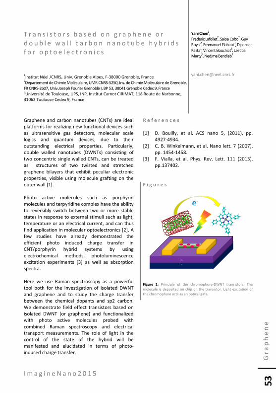
I m a g i n e N a n o 2 0 1 5
Gr
ap
he
ne
53
T r a n s i s t o r s b a s e d o n g r a p h e n e o r d o u b l e w a l l c a r b o n n a n o t u b e h y b r i d s f o r o p t o e l e c t r o n i c s 1Institut Néel /CNRS, Univ. Grenoble Alpes, F-38000 Grenoble, France 2Département de Chimie Moléculaire, UMR CNRS-5250, Ins. de Chimie Moléculaire de Grenoble, FR CNRS-2607, Univ.Joseph Fourier Grenoble I, BP 53, 38041 Grenoble Cedex 9, France 3Université de Toulouse, UPS, INP, Institut Carnot CIRIMAT, 118 Route de Narbonne, 31062 Toulouse Cedex 9, France
Graphene and carbon nanotubes (CNTs) are ideal platforms for realizing new functional devices such as ultrasensitive gas detectors, molecular scale logics and quantum devices, due to their outstanding electrical properties. Particularly, double walled nanotubes (DWNTs) consisting of two concentric single walled CNTs, can be treated as structures of two twisted and stretched graphene bilayers that exhibit peculiar electronic properties, visible using molecule grafting on the outer wall [1]. Photo active molecules such as porphyrin molecules and terpyridine complex have the ability to reversibly switch between two or more stable states in response to external stimuli such as light, temperature or an electrical current, and can thus find application in molecular optoelectronics [2]. A few studies have already demonstrated the efficient photo induced charge transfer in CNT/porphyrin hybrid systems by using electrochemical methods, photoluminescence excitation experiments [3] as well as absorption spectra. Here we use Raman spectroscopy as a powerful tool both for the investigation of isolated DWNT and graphene and to study the charge transfer between the chemical dopants and sp2 carbon. We demonstrate field effect transistors based on isolated DWNT (or graphene) and functionalized with photo active molecules probed with combined Raman spectroscopy and electrical transport measurements. The role of light in the control of the state of the hybrid will be manifested and elucidated in terms of photo-induced charge transfer.
R e f e r e n c e s
[1] D. Bouilly, et al. ACS nano 5, (2011), pp.
4927-4934. [2] C. B. Winkelmann, et al. Nano lett. 7 (2007),
pp. 1454-1458. [3] F. Vialla, et al. Phys. Rev. Lett. 111 (2013),
pp.137402. F i g u r e s
Figure 1: Principle of the chromophore-DWNT transistors. The molecule is deposited on chip on the transistor. Light excitation of the chromophore acts as an optical gate.
Yani Chen1,
Frederic Lafollet2, Saioa Cobo2, Guy Royal2, Emmanuel Flahaut3, Dipankar Kalita1, Vincent Bouchiat1, Laëtitia Marty1, Nedjma Bendiab1

I m a g i n e N a n o 2 0 1 5
Gr
ap
he
ne
54
P o l y m e r C o v a l e n t l y M o d i f i e d G r a p h e n e f o r N o n v o l a t i l e R e w r i t a b l e M e m o r y 1Key Lab for Advanced Materials, Institute of Applied Chemistry, East China University of Science and Technology, 130 Meilong Road, Shanghai 200237, China 2Dep. of Polymer Science and Engineering, College of Chemistry and Chemical Engineering, Shanghai Jiao Tong Un., 800 Dongchuan Road, Shanghai 200240, China
The data storage performance, stability and reliability of the graphene memories have advanced significantly towards practical information storage applications. [1,2] A number of essential strategies can be employed to control and optimize the switching characteristics of graphene memories for practical information storage applications. Covalent functionalization of graphene oxide(GO) or, reduced graphene oxide(RGO) with electroactive polymers is an effective and versatile approach to tuning the electronic properties of graphene. The facile engineering of GO/RGO energy bandgap through polymer functionalization also provides an alternative route to supplement the lithographical patterning of graphene sheets into low dimensional nanostructures and chemical modification of graphene nanoribbons. By using the “grafting to” or “grafting from” method, we have synthesized a new series of soluble polymer-covalently grafted GO/RGO functional materials. Bistable electrical switching effects and non-volatile rewritable memory effects were observed in the ITO/graphene-based polymer/Al sandwiched devices (Fig.1), with small switch-on voltage of about -1~-2 V and the ON/OFF current ratio of more than 103. The non-volatile nature of the ON state and the ability to write, read and erase the electrical states fulfilled the functionality of a rewritable memory. Both the ON and OFF states were stable under a constant voltage stress for more than 104 s and survived up to 108 read cycles at a read voltage of -1.0 V.
R e f e r e n c e s
[1] Y. Chen, B. Zhang,G. Liu et al.,Chem. Soc. Rev.
41(2012)4688–4707.
[2] Y. Chen,G. Liu, C. Wang, W. Zhang, R.-W. Li, L. Wang, Mater. Horiz. 1(2014) 489-506.
F i g u r e s
Figure 1: Typical current density-voltage characteristics of a 0.16 mm2 Al/graphene-based polymer/ITO device.
Luxing Wang1, Cheng Wang1, Xiaodong Zhuang2, Bin Zhang1 and Yu Chen
*1

I m a g i n e N a n o 2 0 1 5
Gr
ap
he
ne
55
B i l a y e r e d M o S 2 / g r a p h e n e s t r u c t u r e s w i t h a R e - a t o m i n a s u p e r c e l l : t h e o r e t i c a l s t u d i e s o f s t a b l e g e o m e t r i e s a n d e l e c t r o n i c p r o p e r t i e s Emanuel Institute of Biochemical Physics, Russian Academy of Sciences, 4 Kosigin Street, 119334, Moscow, Russia
Last time quasi-two-dimensional transition metal dichalcogenides Mo(W)S2(Se2) are taking attention by their semiconducting properties in contrast to semimetallic graphene ones, that they have advantage of their using in semiconductor electronics [1]. At the same time multi-layer structures [2] including bilayers of Mo(W)S2 and graphene (G) are of interest by possibilities of controlling of the electronic and electro-optic properties. We propose new energetically stable MoS2/G90o form of bi-layers with 90o rotated graphene (G) regarding MoS2 layer, and consider by DFT simulations Mo(Re)S2/G structures with renium atom as a doping one in MoS2 supercell, or as an embedded atom between these two layers – MoS2/(Re)/G structures. Insertion of Re atoms into the MoS2-graphene structures determines their metallic properties, especially in MoS2/(Re)/G90o structure (Fig.) with high electronic density of states near Fermi level unlike semi-metallic graphene and Mo(Re)S2/G bilayer [3]. These structures may be important for the application as good metal nanoelements in electronics. Acknowledgements: This work was supported by RSF 14-12-01217. The calculations were performed using resources of the Supercomputer Complex of MSU and the Joint Supercomputer Center of the RAS.
R e f e r e n c e s
[1] H. Terrones, F. López-Urías, M. Terrones, Sci.
Rep. 3 (2013), 1549. [2] A. K. Geim, I. V. Grigorieva, Nature 499
(2013), 419.
[3] B. Sachs, L. Britnell,. T. O. Wehling, A. Eckmann, R. Jalil, B. D. Belle, A. I. Lichtenstein, M. I. Katsnelson, K.S. Novoselov. Appl. Phys. Letters 103 (2013), 251607.
F i g u r e s
Figure 1: Structures with the rhenium atom between MoS2 and G layers: a common view of MoS2/(Re)/G modification(a) and bellow the band energy structure with unit cell in inset (EF= -3.52 eV), the similar schemes of the MoS2/(Re)/G90o bilayer - (b), (EF= -3.38 eV).
L.A. Chernozatonskii and V.А. Demin

I m a g i n e N a n o 2 0 1 5
Gr
ap
he
ne
56
2 D M a t e r i a l s G r o w t h : P r o s p e c t s a n d C h a l l e n g e s Texas Instruments Incorporated, Dallas, TX, USA
The isolation of graphene [1] now almost a decade ago has given rise to the revitalization of an old full set of materials, twodimensional materials (2DM) that have exceptional electrical, chemical and physical properties. Some of the materials under investigation in addition to graphene are hexagonal boron nitride (h-BN), semiconducting, metallic, and superconducting, transition metal dichalcogenides (TMD) with a general chemical formula, MX2 where M is for example equal to Mo, W, Ta, Nb, Zr, Ti, and X = S, Se and Te, and others. While h-BN is an excellent 2D insulator, TMD materials provide what neither graphene nor h-BN can, bandgap engineering that, in principle, can be used to create devices that cannot be fabricated with h-BN and graphene. Therefore, there is hope to integrate these materials for numerous device types for many applications ranging from inkjet printing, photonic applications, flexible electronics, and high performance electronics. However, before the engineering community can develop these products that use 2DM, basic material properties for each application needs full definition so as to select the most appropriate techniques for material preparation and growth. A number of deposition techniques have been used to prepare large area graphene, growth on SiC through the evaporation of Si at high temperatures [2], precipitation of carbon from metals [3], and chemical vapor deposition on Cu [4]. Direct growth of good quality graphene on dielectrics/semiconductors other than SiC has only been reported recently on Ge [5], but not on others. Considering that before 2004 only small flakes of isolated graphene could be grown, the community has madesignificant progress on large area continuous graphene films on Cu and Ge [6].
In addition, there are numerous chemical exfoliating techniques used to form graphene with a range of sizes [7]. CVD graphene and graphene on SiC have been shown exceptional transport properties, equivalent to the best graphene exfoliated from mined graphite. Thin film growth of h-BN on the other hand has been found to be more difficult than graphene nevertheless there are many reports on large area growth on metals but the quality is still not equivalent to h-BN exfoliated from “bulk grown h-BN” when used as a substrate or as a gate dielectric for graphene devices. Transition metal dichalcogenides present altogether different opportunities and difficulties in the preparation of low defect density large area single crystals. Of the many TMDs to select from, a lot of attention has been dedicated to MoS2 because of its long history in rheological applications and availability of naturally occurring crystals and at this time it is used as a platform for materials growth development techniques. Vapor transport, chemical vapor deposition, and molecular beam epitaxy are being developed to produce these materials for initial studies of materials physics device fabrication [8,9]. In this presentation I will present the state of the art results of graphene, h-BN, and a few TMD materials and their prospects for future electronic device applications.
R e f e r e n c e s
[1] Novoselov, K. S. et al. Two-dimensional
atomic crystals. Proceedings of the National Academy of Sciences of the United States of
Luigi Colombo

I m a g i n e N a n o 2 0 1 5
Gr
ap
he
ne
57
America 102, 10451-10453, doi:10.1073/pnas.0502848102 (2005).
[2] Berger, C. et al. Ultrathin Epitaxial Graphite: 2D Electron Gas Properties and a Route toward Graphene-based Nanoelectronics. The Journal of Physical Chemistry B 108, 19912-19916, doi:10.1021/jp040650f (2004).
[3] Karu, A. E. & Beer, M. Pyrolitic Formation of Highly Crystalline Graphite Films. Journal of Applied Physics 37, 2179, doi: 10.1063 /1.1708759 (1966).
[4] Li, X. S. et al. Large-Area Synthesis of High-Quality and Uniform Graphene Films on Copper Foils. Science 324, 1312-1314, doi:10.1126/science.1171245 (2009).
[5] Lee, J.-H. et al. Wafer-Scale Growth of Single-Crystal Monolayer Graphene on Reusable Hydrogen-Terminated Germanium. Science 344, 286-289, doi: 10.1126 /science.1252268 (2014).
[6] Lee, J. H. et al. Wafer-Scale Growth of Single-Crystal Monolayer Graphene on Reusable Hydrogen-Terminated Germanium. Science 344, 286-289, doi: 10.1126 /science.1252268 (2014).
[7] Bonaccorso, F. et al. Production and processing of graphene and 2d crystals. Materials Today 15, 564-589 (2012).
[8] Zhan, Y., Liu, Z., Najmaei, S., Ajayan, P. M. & Lou, J. Large-Area Vapor-Phase Growth and Characterization of MoS2 Atomic Layers on a SiO2 Substrate. Small 8, 966-971, doi:10.1002/smll.201102654 (2012).
[9] Lee, Y.-H. et al. Synthesis of Large-Area MoS2 Atomic Layers with Chemical Vapor Deposition. Advanced Materials 24, 2320- 2325, doi:10.1002/adma.201104798 (2012).

I m a g i n e N a n o 2 0 1 5
Gr
ap
he
ne
58
C o n t r o l l e d f u n c t i o n a l i z e d g r a p h e n e n a n o r i b b o n s p r o d u c e d f r o m c a r b o n n a n o t u b e s 1Institute for Polymers and Composites/I3N, University of Minho, Campus de Azurém, 4800-058 Guimarães, Portugal, 2Department of Chemistry, University of Minho, Campus de Gualtar, 4710-057 Braga, Portugal 3Pole for Innovation in Polymer Engineering (PIEP), Uni of Minho, 4800-058 Guimarães, Portugal, 4International Iberian Nanotechnology Laboratory (INL), Av. Mestre José Veiga, 4715-330 Braga, Portugal 5Computer Science and Technology Center, Uni. of Minho, 4710-057 Braga, Portugal 6Materials Science Centre, School of Materials, Uni. of Manchester, Manchester M13 9PL, U.K. 7Interdisciplinary Nanoscience Center (iNANO) and Department of Physics and Astronomy, Aarhus University, Building 1521, Ny Munkegade, 8000 Aarhus C, Denmark
Graphene nanoribbons (GNR) have received a great deal of attention due their promise for electronics and optoelectronic applications [1]. Recently, the formation of GNR was observed “in situ” by unzipping of carbon nanotubes under ultra-high vacuum scanning tunneling microscopy (UHV STM) [2]. The CNT under observation were functionalized by the 1,3-dipolar cycloaddition reaction [3], in which the concentration of covalently bonded functional groups can be controlled by the experimental functionalization conditions. This functionalization route was responsible for the unzipping of the CNT, and thus the GNR formation by unzipping of functionalized CNT was repeated in ethanol suspension. The present work demonstrates the formation of graphene nanoribbons in solution by unzipping of functionalized carbon nanotubes. The formation of the GNR prepared in solution was studied by UV visible spectroscopy, and the GNR obtained by solvent evaporation were analyzed by Raman spectroscopy, transmission electron microscopy (TEM), X-ray diffraction (XRD) and scanning tunneling microscopy (STM). TEM and STM images demonstrated the formation of few layer graphene ribbons, and this result was confirmed by Raman spectroscopy. Molecular modeling was applied to study the crystalline stacking of functionalized GNRs yielding interlayer distances of 0.51 nm, in agreement with STM and XRD analysis. It was demonstrated that this interlayer distance was required to accommodate the functional groups attached to the graphene. Figure 1 depicts the Raman spectra of the functionalized carbon nanotubes and resulting GNR, showing evidence for the formation of few-layer graphene.
Acknowledgements: The authors acknowledge Fundação para a Ciência e Tecnologia (FCT) for project PEst-C/CTM/LA0025/2013 (Strategic Project - LA 25 - 2013-2014), and for E. Cunha’s PhD grant SFRH/BD/87214/2012. M. Melle-Franco acknowledges support by FCT through the program Ciência 2008 and the project SeARCH (Services and Advanced Research Computing with HTC/HPC clusters) funded under contract CONC-REEQ/443/2005. R e f e r e n c e s
[1] M. Terrones, A. Botello-Méndez, J. Campos-
Delgado, F. López-Urías, Y. Vega-Cantú, F. Rodríguez-Macías, A. Elías, E. Muñoz-Sandoval, A. Cano-Márquez, J. Charlier, H. Terrones, Nano Today, 5 (2010) 351.
[2] M. C. Paiva, W. Xu, M. F. Proença, R. M. Novais, E. Lægsgaard, F. Besenbacher, Nano Letters, 10 (2010) 1764.
[3] M. C. Paiva, F. Simon, R. M. Novais, T. Ferreira, M. F. Proença, W. Xu, F. Besenbacher, ACS Nano 4, (2010) 7379.
Eunice Cunha1,
Helena Rocha1, Maria C. Paiva1, M. Fernanda Proença2, Paulo E. C. Lopes3, Mariam Debs4, Manuel Melle-Franco5, Francis L. Deepak4, Robert Young6, Liv Hornekaer7

I m a g i n e N a n o 2 0 1 5
Gr
ap
he
ne
59
F i g u r e s
Figure 1: Raman spectra of the carbon nanotubes, the functionalized carbon nanotubes and the graphene nanoribbons.
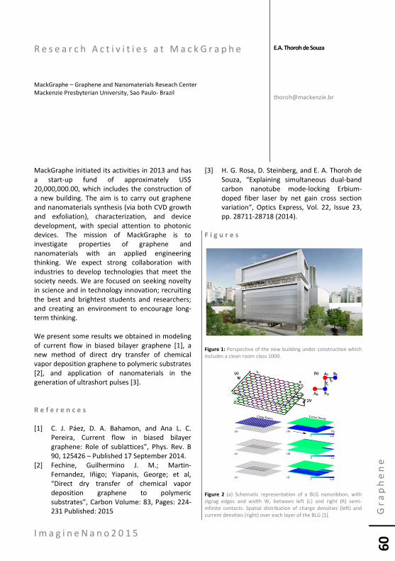
I m a g i n e N a n o 2 0 1 5
Gr
ap
he
ne
60
R e s e a r c h A c t i v i t i e s a t M a c k G r a p h e MackGraphe – Graphene and Nanomaterials Reseach Center Mackenzie Presbyterian University, Sao Paulo- Brazil
MackGraphe initiated its activities in 2013 and has a start-up fund of approximately US$ 20,000,000.00, which includes the construction of a new building. The aim is to carry out graphene and nanomaterials synthesis (via both CVD growth and exfoliation), characterization, and device development, with special attention to photonic devices. The mission of MackGraphe is to investigate properties of graphene and nanomaterials with an applied engineering thinking. We expect strong collaboration with industries to develop technologies that meet the society needs. We are focused on seeking novelty in science and in technology innovation; recruiting the best and brightest students and researchers; and creating an environment to encourage long-term thinking. We present some results we obtained in modeling of current flow in biased bilayer graphene [1], a new method of direct dry transfer of chemical vapor deposition graphene to polymeric substrates [2], and application of nanomaterials in the generation of ultrashort pulses [3].
R e f e r e n c e s
[1] C. J. Páez, D. A. Bahamon, and Ana L. C.
Pereira, Current flow in biased bilayer graphene: Role of sublattices”, Phys. Rev. B 90, 125426 – Published 17 September 2014.
[2] Fechine, Guilhermino J. M.; Martin-Fernandez, Iñigo; Yiapanis, George; et al, “Direct dry transfer of chemical vapor deposition graphene to polymeric substrates”, Carbon Volume: 83, Pages: 224-231 Published: 2015
[3] H. G. Rosa, D. Steinberg, and E. A. Thoroh de Souza, “Explaining simultaneous dual-band carbon nanotube mode-locking Erbium-doped fiber laser by net gain cross section variation“, Optics Express, Vol. 22, Issue 23, pp. 28711-28718 (2014).
F i g u r e s
Figure 1: Perspective of the new building under construction which includes a clean room class 1000.
Figure 2 (a) Schematic representation of a BLG nanoribbon, with zigzag edges and width W, between left (L) and right (R) semi-infinite contacts. Spatial distribution of charge densities (left) and current densities (right) over each layer of the BLG [1].
E.A. Thoroh de Souza

I m a g i n e N a n o 2 0 1 5
Gr
ap
he
ne
61
Figure 3 Schematic of the transfer method and sample after transfer. (a–d) Schematic: (a) graphene/metal and polymer film before transfer. (b) Polymer application step to form the metal/graphene/polymer stack. (c) Peeling of the metal step. (d) Final graphene/polymer stack. [2].
Figure 4 Output spectrum from a dual-wavelength EDFL based on CNT [3].

I m a g i n e N a n o 2 0 1 5
Gr
ap
he
ne
62
D i s e n t a n g l i n g s p i n a n d v a l l e y d y n a m i c s i n m o n o l a y e r M o S 2 b y n o n -e q u i l i b r i u m o p t i c a l t e c h n i q u e s 1IFN-CNR, Piazza L. da Vinci 32, I-20133 Milano, Italy 2Dipartimento di Fisica, Politecnico di Milano, Piazza L. da Vinci 32, I-20133 Milano, Italy 3Dipartimento di Elettronica, Politecnico di Milano and IU.NET, I-20133 Milano, Italy 4Cambridge Graphene Centre, University of Cambridge, 9 JJ Thomson Avenue, Cambridge CB3 0FA, United Kingdom
The ability to control the valley degrees of freedom is the foundation of the emerging field of valleytronics [1]. Atomically thin Transition Metal Dichalcogenides (TMDs) are a promising platform for the implementation of new devices exploiting the valley degrees of freedom [2]. The lack of inversion symmetry, combined with a large spin-orbit interaction, leads to a conduction (valence) band with different spin-polarized minima (maxima) having equal energies [3]. These peculiar properties offer the possibility to develop a new valley-based electronics where information is carried not only by the spin, but also by the crystal momentum at multiple extreme points of the band structure. Any implementation of these concepts, however, needs to consider the robustness of valley and spin degrees of freedom, which are deeply intertwined. To this aim, here we measure separately the spin and valley relaxation dynamics of both electrons and holes in the prototypical TMD MoS2. We disentangle the different processes by the combination of ultrafast optical spectroscopy techniques, i.e. Time Resolved Circular Dichroism (TRCD) and Time Resolved Faraday Rotation (TRFR). TRCD experiments are performed by exciting the sample with an ultrashort circularly polarized pulse, resonant with the optical gap (650 nm), and measuring the difference between the transient absorption response probed by co- and counter- circularly polarized pulses. The transient absorption is measured on a broad energy range including the A (λ = 650 nm) and B (λ = 605 nm) excitonic transitions at K and K’. These measurements reveal an extremely fast intravalley relaxation of the spin of the photoexcited electrons at the bottom of the conduction band. Furthermore, our data demonstrate that the two non-equivalent valleys K
and K’ are strongly coupled and the valley polarization is strongly quenched after few ps [4]. In TRFR experiments the pump pulse, in analogy with TRCD, creates a spin polarized population of electrons/holes in the conduction/valence band, while the rotation angle of the linearly polarized probe pulse is measured by a balanced photodiode bridge technique. We use a two-color TRFR configuration, in which the energy of the probe pulse is tuned well below the absorption gap. In these conditions, the TRFR signal is only sensitive to the helicity-dependent light scattering of the photoexcited electron and hole populations. Since the probe pulse couples with the carrier orbital degree of freedom, the Faraday rotation signal is related to an unbalanced distribution of the photoexcited carrier orbital degrees of freedom. The orbital momentum in MoS2 single layer is locked with the valley index. Thus, the two color TRFR measurements probe exclusively the intervalley dynamics of electrons and holes. The combination of TRFR and TRCD allows us to disentangle intervalley and intravalley dynamics. Both TRCD and TRFR experiments are quantitatively explained by a set of rate equations which take into account intervalley and intravalley relaxation channels. These results are very useful for the engineering of spintronic and valleytronic devices based on single layer TMDs. R e f e r e n c e s
[1] Nebel C. E., Nature Materials 12, 690–691 (2013) [2] Bahnia, K., Nature Nanotech. 7, 488–489 (2012) [3] Zeng, H., Dai, J., Yao, W., Xiao, D., & Cui, X. Nature
Nanotech. 7, 490–3 (2012) [4] Wang, Q., et al. ACS Nano 7, 11087–93 (2013).
S. Dal Conte1,2,
F. Bottegoni2, E. A. A. Pogna2, S. Ambrogio3, D. De Fazio4, A. Lombardo4, M. Bruna4, A.C. Ferrari4, F. Ciccacci2, G. Cerullo2, M. Finazzi2
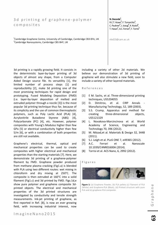
I m a g i n e N a n o 2 0 1 5
Gr
ap
he
ne
63
3 d p r i n t i n g o f g r a p h e n e - p o l y m e r c o m p o s i t e s 1Cambridge Graphene Centre, University of Cambridge, Cambridge CB3 0FA, UK 2Cambridge Nanosystems, Cambridge CB5 8HY, UK
3d printing is a rapidly growing field. It consists in the deterministic layer-by-layer printing of 3d objects of almost any shape, from a Computer Aided Design source file. Its versatility [1], the limited number of process steps [1] and reproducibility [2], make 3d printing one of the most promising techniques for rapid design and prototyping. Fused Modeling Deposition (FMD) (i.e. layer-by-layer deposition of melted and extruded polymer through a nozzle [3]) is the most popular 3d printing technique thus far, because of its simplicity and the use of common thermoplastic polymers, such as Poly Lactic Acid (PLA) [4], Acrylonitrile Butadiene Styrene (ABS) [4], Polycarbonate (PC) [4], etc. However, polymer composites with Young’s Modulus higher than few GPa [5] or electrical conductivity higher than few S/m [6], or with a combination of both properties are still not available. Graphene’s electrical, thermal, optical and mechanical properties can be used to create composites with higher electrical and mechanical properties than the starting materials [7]. Here, we demonstrate 3d printing of a graphene-polymer filament by FMD. Graphene powder produced from methane plasma cracking (Fig1.a) is blended with PLA using two different routes: wet mixing in chloroform and dry mixing at 250°C. The composite is then extruded at 160°C into a solid filament (Fig1.c) and 3d printed by FMD. Figs.1d,e show pure polymer and graphene composite 3d-printed objects. The electrical and mechanical properties of the 3d printed structures are investigated by conductivity and tensile strength measurements. Ink-jet printing of graphene, as first reported in Ref. [8], is now an ever growing field, with increasing industrial interest, now
including a variety of other 2d materials. We believe our demonstration of 3d printing of graphene will also stimulate a new field, soon to include a variety of other layered materials. R e f e r e n c e s
[1] E M. Sachs, et al. Three-dimensional printing
techniques, US5204055 [2] D. Dimitrov, et al. CIRP Annals -
Manufacturing Technology, 52, 189 (2003). [3] S.S. Crump, Apparatus and method for
creating three-dimensional objects, US5121329
[4] L. Novakova-Marcincinova et al. World Academy of Science, Engineering and Technology 70, 396 (2012).
[5] M. Nikzad,et al. Materials & Design 32, 3448 (2011).
[6] S.J. Leigh et al. PLoS ONE 7, e49365 (2012). [7] A.C. Ferrari et al. Nanoscale
10.1039/C4NR01600A (2014). [8] Torrisi et al. ACS Nano, 6, 2992 (2012). F i g u r e s
Figure 1: (a) Graphene Powder, (b) PLA pellets (c) Filament of PLA (White) and Graphene-PLA (Black), (d) Printed structure with pure PLA and (e) graphene-PLA composite.
N. Decorde1,
R.C.T. Howe1, F. Tomarchio1, C. Paukner2, J. Joaug2, K. Koziol2, T. Hasan1, A.C. Ferrari1, F. Torrisi1

I m a g i n e N a n o 2 0 1 5
Gr
ap
he
ne
64
G r a p h e n e / M o S 2 F l e x i b l e P h o t o -d e t e c t o r 1Cambridge Graphene Centre, University of Cambridge, Cambridge, UK 2Electrical Engineering Institute, Ecole Polytechnique Federale de Lausanne, Lausanne, Switzerland
We present a large area, flexible photodetector for visible wavelengths fabricated by stacking centimetre-scale chemical vapor deposited (CVD) graphene and CVD MoS2, both wet transferred onto a flexible polyethylene terephthalate (PET) substrate (fig. 1). In this configuration, MoS2 acts as an absorbing material for visible wavelengths, while graphene is primarily used as a conductive channel for photocurrent flow. When electron-hole pairs are generated in MoS2 upon illumination of the stack, MoS2 donates electrons to the p-doped graphene channel [1], resulting in a decrease of the total source-drain current. In this configuration, the device responsivity can be enhanced either by promoting the injection process from MoS2 to graphene through side-gating using a polymer electrolyte (fig. 2), a technique that is suitable for a flexible platform [2,3], or by increasing the photoconductive gain in the graphene channel by applying larger source-drain voltage. The photodetector has an internal responsivity as high as ~30A/W at 642nm. This is at least two orders of magnitude higher than previously reported values for bulk-semiconductor flexible membranes [4,5] and for other flexible photodetectors based on a combination of graphene and MoS2 [6,7,8]. The photocurrent is stable at different bending angles, with variations less than 15% for radiuses of curvature down to 6cm. R e f e r e n c e s
[1] ] W. J. Zhang, et al. Sci. Rep. 4 (2014). [2] H. Sirringhaus et al. Science 290 (2000) 2123. [3] A. Das et al. Nature Nanotech. 3 (2008) 210.
[4] W. Yang et al. Appl. Phys. Lett. 96 (2010) 121107.
[5] H. C. Yuan et al. Appl. Phys. Lett. 94 (2009) 013102.
[6] F. Withers et al. Nano Lett. 14 (2014) 3987. [7] D. J. Finn et al. J. Mater. Chem. C 2 (2014)
925. [8] Koppens et al. Nature Nanotech. 9, (2014)
780. F i g u r e s
Figure 1: Sketch of the flexible photodetector.
Figure 2: V trans-characteristics of the device at different optical powers.
D. De Fazio1, I. Goykhman1, M.
Bruna1, A. Eiden1, U. Sassi1, M. Barbone1, D. Dumcenco2 K. Marinov2 A. Kis2 and A.C. Ferrari1
I m a g i n e N a n o 2 0 1 5
Gr
ap
he
ne
65
S i n g l e L a y e r M o S 2 u n d e r D i r e c t C o m p r e s s i o n : L o w P r e s s u r e B a n d - g a p E n g i n e e r i n g 1J. Heyrovsky Institute of Physical Chemistry of the ASCR, v.v.i., Dolejškova 2155/3, 182 23, Prague, Czech Republic 2Department of Physical and Macromolecular Chemistry, Faculty of Science, Charles University in Prague, Hlavova 2030, CZ-128 40, Prague 2, Czech Republic
Recently, the unique electronic properties of few layered transition metal dichalcogenides, such as MoS2, have been revealed. Monolayer MoS2 present a direct gap which evolves into an indirect one, as the number of layers increases [1]. Moreover, it has been observed that monolayer MoS2 may turn into an indirect gap semiconductor itself by applying stress, and even transform into a semimetal if the strain is increased [2,3,4]. The regime of the deformation (uniaxial, biaxial, hydrostatic…) and its sign (tensile or compressive) governs the possibility of achieving such electronic transformations, as well as the level of strain required for achieving the changes. In this work, we subject monolayer MoS2 samples to uniaxial compression along the c axis (up to 5 GPa), using a high pressure anvil cell, while monitoring the evolution of the samples with both Raman spectroscopy and photoluminescence measurements. From the evolution of the Raman frequencies of the normal modes with pressure we can distinguish three different electronic states: the direct and indirect gap semiconductor and the semimetal. But interestingly, and in contrast with previous works, the pressure levels required for observing these electronic changes are quite low and they are easily accessible under our experimental configuration: MoS2 samples directly compressed between two hard materials. The change to indirect gap semiconductor is observed just by closing the gem anvil cell, at around 0.5 GPa, and the transition to semimetal is achieved when pressure is increased above 2 GPa. Such results were confirmed by means of theoretical calculations and photoluminescence measurements. The later also provided information about the reversibility of the electronic changes observed under pressure. The transition from direct to indirect semiconductor is
a reversible process; however, once the semimetal state is reached the sample does not recover its semiconductor character after the pressure release. These results open new avenues for the application and development of optoelectronic devices based on these new materials of the family of molybdenum disulphide. Acknowledgements: This work was funded by Czech Science Foundation (project No. 14-15357S). R e f e r e n c e s
[1] Kin F. Mak, Changgu Lee, James Hone, Jie
Shan, Tony F. Heinz, Phys. Rev. Lett. 105 (2010) 2-5.
[2] Xiuming Dou, Kun Ding, Desheng Jiang, Baoquan Sun, ACS Nano, 8 (2014) 7458.
[3] Emilio Scalise, Michel Houssa, Geoffrey Pourtois, Valery Afanas’ev, André Stesmans, Nano Res. 5 (2012) 43.
[4] Hiram J. Conley, Bin Wang, Jed I. Ziegler, Richard F. Haglund, Jr., Sokrates T. Pantelides,Kirill I. Bolotin, Nano Lett. 13 (2013) 3626.
Elena del Corro1
Miriam Peña Álvarez1, Ángel Morales2, Ladislav Kavan1, Martin Kalbac1 and Otakar Frank1

I m a g i n e N a n o 2 0 1 5
Gr
ap
he
ne
66
F i g u r e s
Figure 1: Schematic lateral view of a single layer MoS2 directly compressed in a gem anvil cell. Raman frequencies of the active normal modes of MoS2 as a function of loading pressure.
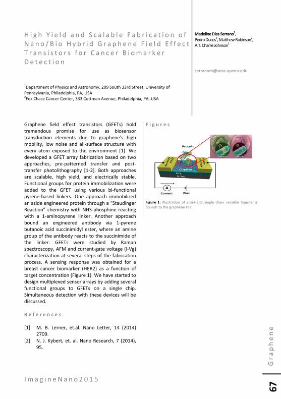
I m a g i n e N a n o 2 0 1 5
Gr
ap
he
ne
67
H i g h Y i e l d a n d S c a l a b l e F a b r i c a t i o n o f N a n o / B i o H y b r i d G r a p h e n e F i e l d E f f e c t T r a n s i s t o r s f o r C a n c e r B i o m a r k e r D e t e c t i o n 1Department of Physics and Astronomy, 209 South 33rd Street, University of Pennsylvania, Philadelphia, PA, USA 2Fox Chase Cancer Center, 333 Cottman Avenue, Philadelphia, PA, USA
Graphene field effect transistors (GFETs) hold tremendous promise for use as biosensor transduction elements due to graphene's high mobility, low noise and all-surface structure with every atom exposed to the environment [1]. We developed a GFET array fabrication based on two approaches, pre-patterned transfer and post-transfer photolithography [1-2]. Both approaches are scalable, high yield, and electrically stable. Functional groups for protein immobilization were added to the GFET using various bi-functional pyrene-based linkers. One approach immobilized an azide engineered protein through a “Staudinger Reaction” chemistry with NHS-phosphine reacting with a 1-aminopyrene linker. Another approach bound an engineered antibody via 1-pyrene butanoic acid succinimidyl ester, where an amine group of the antibody reacts to the succinimide of the linker. GFETs were studied by Raman spectroscopy, AFM and current-gate voltage (I-Vg) characterization at several steps of the fabrication process. A sensing response was obtained for a breast cancer biomarker (HER2) as a function of target concentration (Figure 1). We have started to design multiplexed sensor arrays by adding several functional groups to GFETs on a single chip. Simultaneous detection with these devices will be discussed.
R e f e r e n c e s
[1] M. B. Lerner, et.al. Nano Letter, 14 (2014)
2709. [2] N. J. Kybert, et. al. Nano Research, 7 (2014),
95.
F i g u r e s
Figure 1: Illustration of anti-HER2 single chain variable fragments bounds to the graphene FET.
Madeline Díaz-Serrano1,
Pedro Ducos1, Matthew Robinson2, A.T. Charlie Johnson1
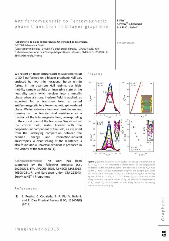
I m a g i n e N a n o 2 0 1 5
Gr
ap
he
ne
68
A n t i f e r r o m a g n e t i c t o F e r r o m a g n e t i c p h a s e t r a n s i t i o n i n b i l a y e r g r a p h e n e 1Laboratorio de Bajas Temperaturas, Universidad de Salamanca, E-37008 Salamanca, Spain 2Dipartimento di Fisica, Universit`a degli studi di Pavia, I-27100 Pavia, Italy 3Laboratoire National des Champs Magn´etiques Intenses, CNRS-UJF-UPS-INSA, F-38042 Grenoble, France
We report on magnetotransport measurements up to 30 T performed on a bilayer graphene Hall bar, enclosed by two thin hexagonal boron nitride flakes. In the quantum Hall regime, our high-mobility sample exhibits an insulating state at the neutrality point which evolves into a metallic phase when a strong in-plane field is applied, as expected for a transition from a canted antiferromagnetic to a ferromagnetic spin-ordered phase. We individuate a temperature-independent crossing in the four-terminal resistance as a function of the total magnetic field, corresponding to the critical point of the transition. We show that the critical field scales linearly with the perpendicular component of the field, as expected from the underlying competition between the Zeeman energy and interaction-induced anisotropies. A clear scaling of the resistance is also found and a universal behavior is proposed in the vicinity of the transition [1]. Acknowledgements: This work has been supported by the following projects: JCYL SA226U13, FPU AP2009-2619, MINECO MAT2013-46308-C2-1-R, and European Union CTA-228043-EuroMagNET II Programme
R e f e r e n c e s
[1] S. Pezzini, C. Cobaleda, B. A. Piot,V. Bellani,
and E. Diez Physical Review B 90, 121404(R) (2014).
F i g u r e s
Figure 1: (a) Rxx as a function of Vg for increasing temperatures at B⊥ = Btot = 7 T. (b) Insulating T dependence of the longitudinal resistance at the neutrality point : the red line is a fit to Rxx∝ exp (Δ/2kBT). Inset: Optical microscopy image of the sample (the scale bar corresponds to 5 μm). (c) Rxx as a function of Vg for increasing B with fixed B⊥ = 5 T, at T 1.2 K. Inset: Gxx as a function of the filling factor for the same values of B. (d) Metallic T -dependence of Rxx. Inset: Gxx as a function of the filling factor for increasing temperatures in strong B.
E. Diez1,
S. Pezzini1,2, C. Cobaleda1 B. A. Piot3, V. Bellani2

I m a g i n e N a n o 2 0 1 5
Gr
ap
he
ne
69
L a r g e - A r e a S i - D o p e d G r a p h e n e : C o n t r o l l a b l e S y n t h e s i s a n d E n h a n c e d M o l e c u l a r S e n s i n g 1Instituto de Física, Universidade de São Paulo, 05508-090 São Paulo SP, Brazil 2Key Laboratory of Advanced Materials (MOE), School of Materials Science and Engineering, Tsinghua University, Beijing, 100084, China 3Department of Materials Science & Engineering, Universidad Carlos III de Madrid, Madrid, Spain 4Department of Physics and Center for 2-Dimensional and Layered Materials, The Pennsylvania State University, University Park, PA 16802, USA 5Institute of Carbon Science and Technology, Shinshu University, Wakasato 4-17-1, Nagano 380-853, Japan 6Advanced Materials Department, IPICYT, Camino a la Presa San José 2055, Col. L omas 4a sección, San Luis Potosí S.L.P., 78216, México 7Department of Physics, Advanced Physics and Astronomy, Rensselaer Polytechnic Institute, 100 Eighth Street Troy, NY, 12180, USA 8Department of Chemistry, Department of Materials Science and Engineering and Materials Research Institute, The Pennsylvania State University, University Park, PA 16802, USA
Chemical doping of graphene with different heteroatoms (e.g. B, N) is becoming a powerful way to tailor its electrical and chemical properties. Extensive studies have been carried out on N- and B-doped graphene. However, there are few reports on Si-doped graphene (SiG) so far. Here we report the controllable synthesis of large-area SiG sheets for the first time using methoxytrimethylsilane (MTMS) and hexane as precursors in a bubbler-assisted chemical vapor deposition (BA-CVD) setup. As a proof-of-concept, their application in probing different organic molecules (e.g. crystal violet, rhodamine B, methylene blue) was successfully demonstrated. We noted that significant enhanced molecular sensing was achieved when SiG was used as a probing surface in virtue of their enhanced Raman scattering effect. This unique enhancement of SiG was explained using ab initio calculations, in which local distortions caused by the presence of Si atoms increase the interaction of the dye molecules with the doped graphene surface, in addition to the presence of an incomplete valence electron caused by the Si atom. Subsequently, the laser electronic excitation generated in SiG is then transferred to the molecule, and give rise to the strong Raman scattering in which both graphene and the molecular vibrations of the dyes are detected [1].
R e f e r e n c e s
[1] Ruitao Lv et al., Adv. Mater. 26 (2014)7593–
7599.
Maria Cristina dos Santos1,
Ruitao Lv2 , Claire Antonelli3, Simin Feng4, Kazunori Fujisawa4, Ayse Berkdemir4, Rodolfo Cruz-Silva5, Ana Laura Elías4, Nestor Perea-Lopez4, Florentino López-Urías6, Humberto Terrones7 & Mauricio Terrones4,5,8

I m a g i n e N a n o 2 0 1 5
Gr
ap
he
ne
70
O p p o r t u n i t i e s a n d c h a l l e n g e s o f
g r a p h e n e a p p l i c a t i o n i n p a s s i v e m i c r o -
a n d m i l l i m e t r e w a v e c o m p o n e n t s
Technical Research Centre of Finland, Tietotie 3, FI-02150 Espoo, Finland
Graphene was first isolated in 2004 and since numerous application concepts based on graphene have been demonstrated [1]. Graphene been recognized from the very beginning as promising candidates for future radio electronics because graphene shows extraordinarily large carrier mobility [2].
Up to now most of the radio related research focuses very much on development of high frequency graphene transistors. In just a few years, high frequency graphene transistors have reached a performance level rivalling the best semiconductor devices that have over sixty years research effort behind them [2,3].
However other unique properties of graphene have not been utilized so much in high frequency analog electronics so far. For example single-layer graphene has very low density of states, which leads to a strong quantum capacitance effect. Quantum capacitance of the graphene depends on applied voltage [4]. This effect has been used in varactors.
No radio circuitry can be built without passive components. It would be important to understand how visible to use graphene for fabrication passive radio components.
In this paper we evaluate opportunities of usage of graphene in passive micro- and millimetre wave components. The paper is presenting the physical properties of graphene in terms
of its application in passive micro and millimeter wave components;
review of applications of graphene in passive components including antennas, transmission lines, inductors and varactors
new type of a phase shifter based on effect of dependence of quantum capacitance on
applied voltage are proposed and theoretically analyzed.
Analysis shows that high resistance of single layer graphene is the main challenge of usage of graphene in passive devices. Though graphene is the best electrical conductor known, it is mono-atomic and thus the surface resistance is very high compared to metals at micro and mm-waves frequencies, even with the possibility of doping and electric field biasing of graphene. In these frequency ranges graphene is thus mostly a moderate to bad conductive surface. At microwave and mm-wave frequencies, graphene conductivity is essentially real and the electric field bias allows controlling this resistivity over a certain range.
The picture is quite different at terahertz frequency range above 500 GHz, as a result of the plasmonic nature of the imaginary conductivity allowing plasmonic modes. At terahertz electric field affects strongly the imaginary part of the graphene conductivity. This mode can be used in tunable terahertz devices, for example terahertz antennas and filters.
R e f e r e n c e s
[1] A. K. Geim & K. S. Novoselov , Nature Materials, 6, (2007), pp 183 - 191
[2] P. Avouris, Nano letters, 10, (2010), pp 4285–4294.
[3] F. Schwierz, Nature nanotechnology, 5, (2010), pp 487–496.
[4] A.S Mayorov, K.S Novoselov, M.I Katsnelson, A.K Geim, 105, (2010) Physical review, pp 136801(4).
[5] J. S. Gómez-Díaz and J. Perruisseau-Carrier, International Symposium on Antennas and Propagation (ISAP12), Nagoya (Japan), (2012), pp 239-242.
Vladimir Ermolov, Jan Saijets

I m a g i n e N a n o 2 0 1 5
Gr
ap
he
ne
71
H i g h S p e e d – L a r g e A r e a – N o n d e s t r u c t i v e G r a p h e n e C h a r a c t e r i z a t i o n 1das-Nano, P.I. Mutilva Baja Calle G-6. E-31192 Mutilva Baja, Navarra. Spain 2CIC nanoGUNE. Tolosa Hiribidea, 76. E-20018 Donostia-San Sebastián, Spain 3Graphenea. Tolosa Hiribidea, 76. E-20018 Donostia-San Sebastián, Spain 4Dept. Fisica Fundamental, Universitat de Barcelona. C. de Martí i Franquès, 1,08028 Barcelona,Spain
In this paper we will present a new, ultra-fast device (Figure 1) for quality inspection of thin film materials. This machine inspects and determines the quality of thin film materials such as graphene (mono-layer and multilayer), PEDOT or ITO by a repeatable and reproducible [1] measurement process. The materials cited above are currently characterized by nano-scale tools (such as confocal Raman Spectroscopy, Atomic Force Microscopy or Transmission Electron Microscopy), and/or macro-scale methods (for example van der Pauw resistivity technique or optical microscopy) [2]. Our Thin Film Inspector covers the gap between the nano-scale tools and the macro-scale methods allowing the ultra-fast determination of the existence of inhomogeneities in the material. Our Thin Film Inspector is non-invasive (metallic contacts are not required), non-destructive (thin film material is not modified) and non-ionizing. Furthermore, our Thin Film inspector can measure the full area of the sample under examination and provide a quality map (Figure 2) at a very high speed (over 10.000 mm2,@ 1 mm2 resolution), and with a spatial resolution of 100 μm. R e f e r e n c e s
[1] Rouhi et al., Nano Research, (2012), Volume
5, Issue 10, pp 667-678 [2] Buron et al., Nano Letters (2012), Volume 12
Issue 10, pp 5074–5081
F i g u r e s
Figure 1: Thin Film Inspector.
Figure 2: Quality maps of several samples of Monolayer Graphene.
David Etayo1, Alex Lopez1,
Magdalena Chudzik1, Luis E. Hueso2, Amaia Zurutuza3, Javier Tejada4 and Eduardo Azanza1

I m a g i n e N a n o 2 0 1 5
Gr
ap
he
ne
72
I n t e r n a t i o n a l S t a n d a r d i z a t i o n o n G r a p h e n e - b a s e d N a n o t e c h n o l o g y 1PTConsulting, 45144 Essen, Germany 2Karlsruher Institut für Technologie, 76344 Eggenstein-Leopoldshafen, Germany
International standards are more and more recognized as a tool for dissemination and exploitation of research results for developing industrial applications. To be successful in facilitating this transition, the process of standardization needs to be started as early as possible even if fundamental research has not established a satisfactory level of knowledge and industrial fabrication processes are not mature enough for commercialization. In the area of nanotechnology, international standardization started 10 years ago driven by the International Electrotechnical Commission (IEC) and the International Standardization Organization (ISO) with the establishment of the two technical committees IEC/TC 113 and ISO/TC 229. Currently, over 100 standards are published or under development. They cover a broad range of nanotechnologies topics from nanomaterials to nano-enabled batteries and nano-enabled photovoltaics as well as standards regarding environmental, health and safety aspects and the development of a comprehensive nanotechnology vocabulary. With the rise of graphene-based technologies, this topic was adopted by the committees IEC/TC 113 and ISO/TC 229 leading to the establishment of currently 8 graphene projects. On the European level, graphene standardization was identified as an important activity within the Graphene Flagship. Here standardization is not only needed from a technical point of view to ensure that material specifications and measurement methods are developed in consensus with the involved stakeholders. It also helps to improve the exchange of information across work packages and
supports the development process along the roadmap from research to commercialization. This workshop will introduce to the international standardization on graphene technologies and present the status reached. This includes the activities within the IEC and ISO nanotechnology committees and the recently established Graphene Flagship Standardization Committee which is now organizing the CENELEC Workshop on Specifications for Graphene Related Materials (WS SGRM). All this activities are well linked together to ensure the establishment of a comprehensive system of standards for graphene-based technologies. Furthermore, it should become clear how important it is especially for the industry to actively participate in the standardization process and what kind of service IEC and ISO provide to make this investment most efficient for its stakeholders. .
Alexandra Fabricius1 and Norbert Fabricius
2

I m a g i n e N a n o 2 0 1 5
Gr
ap
he
ne
73
F L A G - E R A : T h e F E T F l a g s h i p E R A - N E T
MINECO, Spain
The FET Flagship ERA-NET, called FLAG-ERA, gathers national and regional funding organisation with the goal of supporting the FET Flagship initiatives and more generally the FET Flagship concept. Most funding organisations in Europe participate, either directly or as associated members. The project also fosters international cooperation with funding organisations outside Europe. FLAG-ERA thus offers a platform to coordinate a wide range of sources of funding towards the realization of very ambitious research goals. FLAG-ERA contributes to the construction of the two Flagship initiatives on Graphene and Human Brain research, and also offers support to the four non-selected pilots to progress towards their goals with adapted means. It does so through a range of activities: • In order to enable researchers funded through various sources to work in tight cooperation with each other in the context of the two Flagships, the funding organisations in FLAG-ERA coordinate their funding framework conditions. • In order to enhance complementarities and synergies of regional, national and European research programmes and initiatives, the funding organisations share information on these programmes and initiatives, identify gaps and overlaps, and can thus adapt their thematic program and launch new initiatives according to the identified needs. In particular, they launch Joint Transnational Call (JTC) enabling researchers from different countries to propose joint contributions to the Flagships. The FLAG-ERA JTC 2015 was closed on January 27th 2015. A total of 108 proposals were submited
with 408 participats. The proposals will be assessed by an independent international Scientific Evaluation Panel (SEP) with the help of external reviewers, experts in the Flagship topic/areas. The final funding decision by the National and/or Regional Research Funding Organisations (NRFOs) participating in the JTC is expected by September 2015. • Additionally, in order to encourage the actual construction of the Flagships and take-up of their results, the funding organisations organise networking sessions for the research communities and other stakeholders, including industry. The activities in FLAG-ERA are organised around periodic events gathering all stakeholders and structured in sessions dedicated to the various objectives and related tasks of the project. All activities are done with the long-term vision of the Flagship programme in mind, and the project extends slightly beyond the ramp-up phase in order to accompany the transition to the fully operational phase of the Flagships. F i g u r e s
Severino Falcon

I m a g i n e N a n o 2 0 1 5
Gr
ap
he
ne
74
T u n i n g g r a p h e n e p r o p e r t i e s b y a m u l t i - s t e p t h e r m a l r e d u c t i o n p r o c e s s 1Instituto Nacional del Carbón, INCAR-CSIC, Apdo. 73, 33080 Oviedo, Spain. 2REPSOL, Centro de Tecnología, Carretera de Extremadura, km 18, 28935 Mostoles, Madrid
The chemical methods for producing graphene materials, via the formation of graphite oxide which must be subsequently exfoliated and reduced to obtain the final graphene, are among the most valuable due to their simplicity and easy scalability. The characteristics of the graphene materials obtained (rGO), which will determine their applicability, are greatly affected by the experimental conditions.[1,2] In any case, the use of single-step thermal treatment does not allow the properties of the materials obtained to be tuned as once the final temperature has been fixed, the resulting properties (C/O ratio, BET surface area, processability into suitable electroders, etc.) are also fixed. The aim of this work is to design a route for the preparation of rGOs of enhanced BET surface area as well as maximizing their suitability as electrodes in energy devices. For that, a GO obtained by a modified Hummers method was thermally exfoliated/reduced at 700 and 1000ºC by two single step procedures (ramp and flash pyrolisis) and by a novel multi-step procedure. The ramp pyrolisis in a single step gave rise to rGOs with low BET surface areas (~200 m2g-1) which are easily conformed into stable electrodes (Figure 1a). In contrast, by flash pyrolisis in a single step, high BET surface areas were obtained (~500 m2g-1) but it is not possible to conform them into stable electrodes (Figure 1b). By using the multi-step procedure developed herein it is possible to prepare rGOs that have an increased BET surface area (compared to that of the material prepared by the single-step ramp-heated material) and that are easily conformed into stable electrodes for electrochemical energy storage devices (Figure 1c). SEM images of the
rGOs indicate the formation of tridimensional structures derived from the expansion of the graphite oxide on heating, which is the factor responsible for the development of porosity in these graphene materials. In the case of the flash-pyrolized sample (Figure 2a) cavities with sizes more in the range of mesopores are observed, contributing to an increment in the BET surface area and to the loss of suitability as electrodes. These structures are not so abundant in the ramp-heated sample, which explains its lower BET surface area (Figure 2b). An intermediate situation is obtained by the multi-step procedure, which explains the high BET surface area and good suitability as electrode of these materials. Acknowledgements: The authors thank REPSOL for their financial support; project SAVE Dr. P. Alvarez also acknowledges MICINN for her Ramon y Cajal contract. Work patented (ref: EP14382352.4).
R e f e r e n c e s
[1] McAllister MJ et al. Chem Mater 19 (2007)
4396. [2] Botas C et al. Carbon 50 (2012) 275.
Laura Fernández-García1,
Patricia Álvarez1, Marcos Granda1, Clara Blanco1, Ricardo Santamaría1, Patricia Blanco1, Zoraida González1, Uriel Sierra1, Antonio Páez2, Rosa Menéndez1*

I m a g i n e N a n o 2 0 1 5
Gr
ap
he
ne
75
F i g u r e s
Figure 1: Thin Film Inspector.
Figure 2: Quality maps of several samples of Monolayer Graphene.

I m a g i n e N a n o 2 0 1 5
Gr
ap
he
ne
76
T h e E u r o p e a n r o a d m a p f o r s c i e n c e a n d t e c h n o l o g y o f g r a p h e n e a n d r e l a t e d m a t e r i a l s Cambridge Graphene Centre, Cambridge CB3 OFA, UK
I will present the science and technology roadmap for graphene, related two-dimensional crystals, and hybrid systems developed within the framework of the European Graphene Flagship[1]. I will focus on some emerging application areas, such as the integration of graphene with silicon photonics, and flexible devices. R e f e r e n c e s
[1] AC. Ferrari et al., Nanoscale, 2014, DOI:
10.1039/C4NR01600A
Andrea C. Ferrari

I m a g i n e N a n o 2 0 1 5
Gr
ap
he
ne
77
H a r n e s s i n g l i g h t t o t u n e t h e t o p o l o g y o f m a t e r i a l s 1Ins. de Física Enrique Gaviola (CONICET) and Univ. Nacional de Córdoba, Argentina 2Universidad Técnica Federico Santa María, Valparaíso, Chile 3CONICET, Centro Atómico Bariloche and Instituto Balseiro, Comisión Nacional de Energía Atómica, 8400 San Carlos de Bariloche, Argentina
The understanding lightmatter interaction has led to many practical applications. Raman spectroscopy, an outstanding tool for graphene characterization, is a prominent example. But beyond characterization, several studies proposed much deeper effects of laser illumination on the electronic properties of a material like switching off the conduction in graphene [1,2], thereby allowing to tune the material's response with optical means, or even inducing new (tunable) topological phases in otherwise trivial materials [1,3,4] (i.e. a Floquet topological insulator ). The latter is very promising as it would enormously expand the playground of topological insulators to a broader set of materials. Recently, laserinduced bandgaps have been experimentally verified at the surface of a topological insulator [5] adding much thrill to this area. In this talk I will provide an overview of the recent developments in this field with a focus on the generation of Floquet chiral edge states in graphene [6,7] (Fig. 1(a)), bilayer graphene [8] and other materials [9,10]. The emergence of a Hall response without Landau levels [11,12] (see scheme in Fig. 1(b)), similarities and differences with the integer quantum Hall effect (like the breakdown of the connection between usual topological invariants and the Hall conductance [11]), and a few open problems will also be highlighted.
R e f e r e n c e s
[1] T. Oka and H. Aoki, Phys. Rev. B 79 (2009)
081406. [2] H. L. Calvo, H. M. Pastawski, S. Roche, and L.
E. F. Foa Torres, Appl. Phys. Lett. 98 (2011) 232103;H. L. Calvo, P. M. PerezPiskunow, S. Roche, and L. E. F. Foa Torres, Appl. Phys. Lett. 101 (2012) 253506 (2012).
[3] N. H. Lindner, G. Refael, and V. Galitski, Nat. Phys. 7 (2011) 490.
[4] T. Kitagawa, T. Oka, A. Brataas, L. Fu, and E. Demler, Phys. Rev. B 84 (2011) 235108.
[5] Y. H. Wang, H. Steinberg, P. JarilloHerrero, and N. Gedik, Science 342 (2013) 453.
[6] P.M. PerezPiskunow, G. Usaj, C. A. Balseiro, and L. E. F. Foa Torres Phys. Rev. B, 89 (2014) 121401(R).
[7] G. Usaj, P. M. PerezPiskunow, L. E. F. Foa Torres, and C. A. Balseiro Phys. Rev. B, 90 (2014) 115423.
[8] E. Suárez Morell and L. E. F. Foa Torres Phys. Rev. B, 86 (2012) 125449.
[9] H. L. Calvo, L. E. F. Foa Torres, P. M. PerezPiskunow, C. A. Balseiro, G. Usaj, to be published .
[10] V. Dal Lago, L. E. F. Foa Torres, to be published .
[11] L. E. F. Foa Torres, P. M. PerezPiskunow, C. A. Balseiro, and G. Usaj Phys. Rev. Lett., 113 (2014) 266801.
[12] Related publications and updates available at http://nanocarbon.famaf.unc.edu.ar/
P. M. PerezPiskunow1 , H. L. Calvo1 , V. Dal Lago1 , E. Suárez Morell2 , C. A. Balseiro3 , G. Usaj3 and Luis E. F. Foa Torres
1
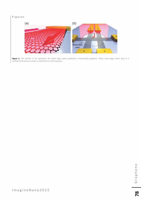
I m a g i n e N a n o 2 0 1 5
Gr
ap
he
ne
78
F i g u r e s
Figure 1: The scheme in (a) represents the chiral edge states predicted in illuminated graphene. These chiral edge states lead, in a multiterminal setup as shown in panel (b), to a Hall response.

I m a g i n e N a n o 2 0 1 5
Gr
ap
he
ne
79
S o l a r e n e r g y c o n v e r s i o n i n v a n d e r W a a l s h e t e r o s t r u c t u r e s 1Institute of Photonics, Vienna University of Technology, Gusshausstrasse 27-29, 1040 Vienna, Austria 2Institute for Theoretical Physics, Vienna University of Technology, Wiedener Hauptstrasse 8-10,1040 Vienna, Austria
Photovoltaic cells for solar energy harvesting are today mainly made out of crystalline semiconductors or organic compounds. Beside the high production costs, crystalline semiconductor cells have the drawback of being heavy and bulky. Organic cells, on the other hand, suffer from low carrier mobility and short lifetime of the organic material. To overcome these drawbacks, we engineered a new type of solar cell based on atomically thin transition metal dichalcogenide (TMDC) layers. Due to the thickness of the used materials the advantages of low raw material costs, high flexibility and semi-transparency are intrinsic parameters. This, combined with the wide range of available band gaps and the good carrier mobility make atomically thin TMDC crystals a promising candidate for next generation solar cells[1]. Recent work demonstrated that atomically thin WSe2 can be electrostatically doped such that hole and electron conduction is achieved and that it can be used to realize a lateral hetero-junction which can be operated as a solar cell[2]. The main drawback of the mentioned structure is the small interaction area. To overcome this limitation, we fabricated planar van der Waals heterojunctions by stacking two[3], and also multiple, atomically thin TMDC layers. Figure 1a shows that such a planar p-n can indeed be used for efficient solar energy harvesting. Besides measurements of electrical transport and the photovoltaic properties, we will present photoluminescence measurements that clarify the working principle of these devices. In addition we will present improved cells, formed by a triple TMDC heterojunction as schematically depicted in Figure 1b.
R e f e r e n c e s
[1] D. Jariwala et al., ACS Nano, 8 (2014) 1102-
1120. [2] A. Pospischil et al., Nature Nanotechnology, 9
(2014) 257-261. [3] M.M. Furchi et al., Nano Letters, 14 (2014)
4785-4791. F i g u r e s
Figure 1: (a) I-V characteristic of the MoS2 – WSe2 heterostructure device under optical illumination with Popt =180…6400 W/m2. (b) Schematic illustration of a triple junction heterostructure device.
Marco M. Furchi1,
Andreas Pospischil1, Armin A. Zechmeister1, Florian Libisch2, Joachim Burgdörfer2 and Thomas Mueller1

I m a g i n e N a n o 2 0 1 5
Gr
ap
he
ne
80
G r a p h e n e O x i d e B a s e d E l e c t r o d e s f o r S u p e r c a p a c i t o r s w i t h E n h a n c e d C y c l i c P e r f o r m a n c e Centre for Advanced Photonics and Electronics, Department of Engineering, University of Cambridge, 9 J. J. Thomson Ave., CB3 0FA, Cambridge, UK.
Graphene and graphene-based materials have attracted significant recent attention because of their unique properties and have emerged as a new class of promising electrode material in supercapacitors. Among the various approaches, chemical exfoliation of graphite has provided an affordable route to the large scale processing of graphene-based materials. The most common chemical means of graphite exfoliation is the use of strong oxidizing agents to yield graphene oxide (GO). For GO, contiguous aromatic lattice of graphene is interrupted by epoxides, alcohols, ketone carbonyls and carboxylic groups. These surface oxides make GO electrically insulating but, hydrophilic and thus, allow intercalation of water and polar solvent molecules between the GO layers. Although GO is not a preferred electrode material for supercapacitors due to its electrically insulating nature, in this study we exploit the ability of GO to interact with organic solvents to enhance the cyclic performance of GO based supercapacitors. Deviating from the normal supercapacitor behaviour, for GO based supercapacitors, a gradual increase in specific capacitance was observed with the cycle number. Free standing, flexible GO paper was synthesised using graphite oxide derived from vein graphite following Hummer’s method and used as the electrode material. The morphology and chemical structure of the material were characterized by means of scanning electron microscopy, Raman spectroscopy, X-ray diffraction and Fourier transform infrared spectroscopy. Thermal properties were investigated using thermo gravimetric analysis. The electrochemical properties of as obtained GO paper were investigated, together with its thermally reduced component (r-GO) for comparison. For electrochemical characterisation, two-electrode symmetrical supercapacitor cells were constructed and characterized by cyclic voltammetry and electrochemical impedance spectroscopy. Tetraethylammonium tetrafluoroborate (TEABF4) in
Propylene Carbonate (PC) was used as the electrolyte. The results showed that for GO based supercapacitors, the specific capacitance increased by approximately six times (from 71 mF g-1 to 422 mF g-1) after 24,000 cycles. After 24,000 cycles, the specific capacitance decreased gradually, but even after 85,000 cycles the value did not drop below the initial specific capacitance (258 mF g-1 after 85,400 cycles). However, for r-GO based supercapacitors, the specific capacitance decreased gradually with cycle number revealing the usual supercapacitor behaviour. This confirms that, the enhanced cyclic performance of GO based supercapacitors can be attributed to the presence of functional groups on GO. Their ability to interact with PC, allows PC molecules to intercalate between the graphene sheets, facilitating exfoliation of graphene sheets as confirmed by X-ray diffraction data. Subsequent increase in the electrochemically accessible surface area of the electrode material increases the specific capacitance of GO based supercapacitors. Although GO based supercapacitors exhibit relatively lower specific capacitance due to the electrically insulating nature of GO, when GO is mixed with a suitable conductive electrode material, the resulting composite may benefit from the presence of GO to enhance the cyclic performance. R e f e r e n c e s
[1] Hummers Jr., W. S., Offeman, R. E, J. Am. Chem.
Soc., 80 (1958), 1339–1339 [2] Dikin, D. A. et al. , Nature Letters, 448 (2007),
457-460
D. Thanuja L. Galhena Bernhard C. Bayer, Stephan Hofmann and Gehan A. J. Amaratunga

I m a g i n e N a n o 2 0 1 5
Gr
ap
he
ne
81
G r a p h e n e - b a s e d e l e c t r o n i c s f o r b i o m e d i c a l a p p l i c a t i o n s Walter Schottky Institut, Technische Universität München, Am Coulombwall 4, Garching, Germany
Graphene and graphene-based materials possess a rather exclusive set of physicochemical properties holding great potential for medical and biomedical applications. In this presentation, I will provide an overview on fundamentals and applications of several graphene-based technologies and devices, namely solution-gated field-effect transistors and microelectrode arrays based on CVD-grown graphene. I will first introduce the science and technology of such electronic devices, both on rigid and flexible substrates, discussing the influence of the intrinsic properties of CVD graphene (e.g. grain boundaries) and comparing their performance with other competing technologies. The presentation will further discuss on the functionalization of these devices aiming at the introduction of specific sensing mechanisms, which is of particular relevance for the development of chemical and biochemical sensors. Based on these technologies, I will also report on experiments aiming at the bidirectional communication with electrogenic cells as well as the detection of neurotransmitters, suggesting a bright future for graphene-based technologies in the field of neuroprosthetics.
Jose A. Garrido

I m a g i n e N a n o 2 0 1 5
Gr
ap
he
ne
82
S t i f f e n i n g g r a p h e n e b y c o n t r o l l e d d e f e c t c r e a t i o n 1Departamento de Física de la Materia Condensada, Universidad Autónoma de Madrid, 28049, Madrid, Spain
Graphene, due to its extremely high in plane stiffness and low bending rigidity, presents important out of plane thermal fluctuations crucial for the understanding of its mechanical properties. In this work we measure the variation of the stiffness of graphene with induced vacancy density using AFM nanoindentations. Unlike predicted, we find that the stiffness of graphene increases with defect content until a vacancy density of 0.2 percent, where it doubles its initial value. For higher defect density the elastic modulus exhibits a decreasing tendency. We attribute the initial increase in stiffness to the quenching of the out of plane oscillations of graphene due to defects [1]. In order to validate this interpretation we also study the dependence of the elastic modulus with strain. We observe an increase of the Young’s modulus at pre-strains higher than 0.5 percent where it again doubles its initial value. R e f e r e n c e s
[1] Lopez-Polin et al. Nature Physics accepted
C. Gómez-Navarro1,
G. López-Polín1, V. Parente, F. Guinea, M. I. Katsnelson, F. Pérez-Murano, J. Gómez-Herrero1

I m a g i n e N a n o 2 0 1 5
Gr
ap
he
ne
83
G r a p h e n e r e s e a r c h a t I C N 2 1ICN2 - Institut Català de Nanociència i Nanotecnologia 2CSIC - Consejo Superior de Investigaciones Científicas Edifici ICN2, Campus UAB, 08193 Bellaterra, Spain
ICN2 is turning research into marketable technologies with the expertise of over 200 scientists and technicians that put their work in the whole value chain, from fundamental research all the way to design, fabrication, and evaluation of nanotechnology-based devices. The Institute offers a full suite of advanced instruments available for research and innovation in fields such as energy, biosystems (medical and environmental), and information and communication technologies. Our activities take place in a stimulating environment, close to Barcelona, where over 500 researchers and 200 technicians work on materials science and micro/nanotechnologies within the Barcelona Nanotechnology Cluster - Bellaterra (www.bnc-b.net), a cluster comprising several public and private research centers, the Universitat Autónoma de Barcelona, and the ALBA Synchrotron. Graphene research is one of the cornerstones of the work developed by ICN2’s multidisciplinary groups. The Institute promotes collaboration among scientists from diverse backgrounds (physics, chemistry, biology, engineering) to conduct basic and applied research, always seeking interaction with local and global industries. In this sense, graphene is one of the basic tools that ICN2 uses to develop its science and technology. The ultimate goal is to produce devices for real life applications, which can be only developed from the discovery and deep knowledge of the most fundamental aspects of the materials and nanostructures.
Graphene research at ICN2
encompasses four major
areas:
Predictive modelling of materials and devices. Theoreticians and experimentalists work together to create, validate, and refine models that predict the behavior of graphene. Production methods. ICN2 conducts research to achieve higher levels of control over size, shape, and layers, to develop large-scale fabrication processes and to produce customized graphene-based materials. Characterization and testing. ICN2 research groups define properties of graphene, measure electronic thermal and quantum phenomena in graphene-based devices, and test how graphene reacts to realistic external forces. Device design, fabrication and evaluation. Graphene-based biosensors, solar cells, supercapacitors, and information and communication devices are being developed. F i g u r e s
Figure 1: Simulated charge mobility of polycrystalline graphene. D.V. Tuan, J. Kotakoski, T. Louvet, F. Ortmann, J. C. Meyer, and S. Roche, Nano Letters, 13(4), 1730-1735 (2013).
Pedro Gómez-Romero1,2
www.icn2.cat/graphene [email protected]
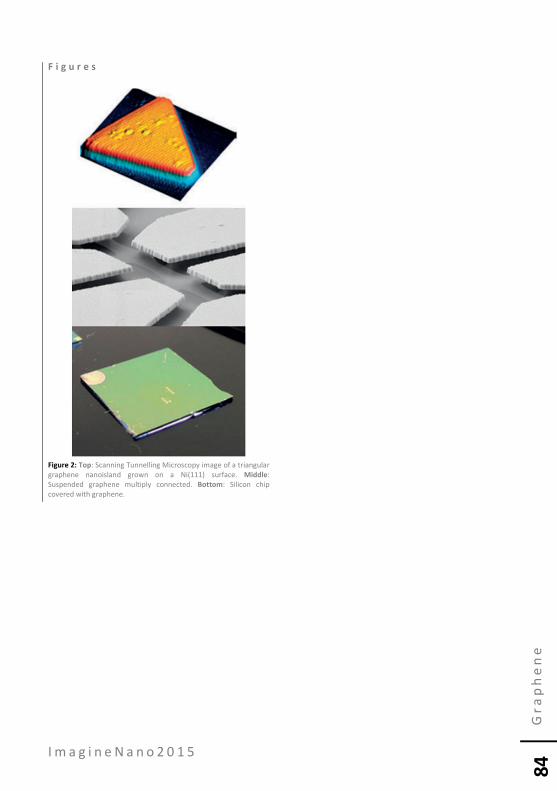
I m a g i n e N a n o 2 0 1 5
Gr
ap
he
ne
84
F i g u r e s
Figure 2: Top: Scanning Tunnelling Microscopy image of a triangular graphene nanoisland grown on a Ni(111) surface. Middle: Suspended graphene multiply connected. Bottom: Silicon chip covered with graphene.

I m a g i n e N a n o 2 0 1 5
Gr
ap
he
ne
85
H y b r i d p o l y o x o m e t a l a t e / r e d u c e d g r a p h e n e o x i d e c o m p o s i t e s f o r s u p e r c a p a c i t o r s 1Institut Català de Nanociència i Nanotecnología, ICN2-CSIC,UAB Campus 08193 Bellaterra, Spain. Phone: +34 937373608 2Present Address: European Commission, DG Joint Research Centre, Institute for Energy and Transport, P.O. Box 2, 1755 ZG Petten, The Netherlands
In this work, we present the novel synthesis and electrochemical study of polyoxometalate-graphene oxide hybrid materials to be used as electrode in Supercapacitors (SCs). The synthesis involves the reduction of graphene oxide (GO) with simultaneous incorporation of polyoxometalate (POM).1 The existence of the strong chemisorption between polyoxometalate and graphene oxide makes it possible to construct stable hybrid carbon structures. Hybrid materials were carried out in a single step by means of a hydrothermal treatment (120 °C, 24 h) of an aqueous solution of polyoxometalate: H3PMo12O40.10H2O (PMo12) and exfoliated graphene oxide (GO). The resulting materials (labeled HT-RGO-PMo12) was filtered-off, washed and dried at 50 °C overnight. The amount of POM impregnated was determined by TGA. A similar treatment of a GO sample without POM added was carried out for comparison (sample HT-RGO). Figure 1 shows the HR-TEM images of the blank HT-RGO sample (Fig, 1A) and HT-RGO-PMo12 (Fig. 1B). The presences of the inorganic POM clusters on the surface graphene are clearly detected in the latter image, and are evenly distributed at a truly molecular level and no agglomerate or nanocrystal could be detected. The electrochemical characterization of the hybrid materials was tested by cyclic voltammetry and galvanostatic charge-discharge test in two- and three- electrodes configurations, where platinum wire and Ag|AgCl were used as counter and reference electrode, respectively. 1 M H2SO4 was the electrolyte.
R e f e r e n c e s
[1] [1] Suárez-Guevara, J.; Ruiz, V.; Gomez-
Romero, P. J. Mater. Chem. A, 2 (2014), 1014 – 1021.
F i g u r e s
Figure 1: HR-TEM images of HT-RGO (A) and HT-RGO-PMo12 (B). Scale bars are 10 nm.
Jullieth Suarez-Guevara1, Vanesa Ruiz1,2 and
Pedro Gomez-Romero1*
[email protected], jullieth.suarez@gmail,com, [email protected]

I m a g i n e N a n o 2 0 1 5
Gr
ap
he
ne
86
G r a p h e n e d r u m m e c h a n i c a l r e s o n a t o r s d e t e c t e d b y m i c r o w a v e s National Physical Laboratory, Teddington TW11 0LW, UK 1Imperial College London, Department of Materials, London SW7 2AZ, UK 2Wroclaw University of Technology, ul. Janiszewskiego, 11/17, 50-372 Wroclaw, Poland
The self-supporting monolayer material which is graphene has excited enormous interest over the ten years since its discovery due to its remarkable electrical, mechanical, thermal and chemical properties. We describe transfer of graphene onto a patterned SiO2/Si substrate which provides freely suspended graphene drums ranging in size from 2m to 40m which are being explored as nano-electromechanical (NEMS) resonators. An SEM image of an array of patterned structures for our graphene NEMS resonators is shown in Fig. 1a. An AFM scan across a 5m square graphene suspended membrane is shown in fig. 1b). As electromechanical devices become smaller, approaching the nanoscale, the oscillation displacement amplitude scales down in proportion to size. Thus new ultra-sensitive transducer techniques and low dissipation excitation schemes are needed to operate NEMS sensors. Microwave measurement using high Q resonators becomes attractive due to the high sensitivity of frequency measurement and the very low phase noise from synthesized microwave sources, in contrast with optical systems. We have developed a novel near-field microwave probe system which is able to simultaneously excite and readout the oscillation of a range of mechanical resonators, from hundreds of microns to sub-micron size. By using a quarter wave microwave coaxial resonator with the open end connected to a sharp tip we can produce a very localized intense microwave field in a very limited region close to the tip. The spatial range of this high field region is on the order of the radius of curvature of the tip, which can be, comparable to the smallest mechanical resonator dimensions.
We report experimental data on these drums using a variety of microwave excitation and readout methods. An important issue is that there is strong coupling between graphene and microwave fields. This relates to the relatively close matching of the impedance of free space, or a confined geometry like a microwave resonator, and the sheet resistance of high quality graphene [1], making the microwave method particularly suitable for application to graphene NEMS resonator based sensors [2]. R e f e r e n c e s
[1] L. Hao, J. Gallop, S. Goniszewski, O.
Shaforost, N. Klein and R. Yakimova, ‘Non-contact method for measurement of the microwave conductivity of graphene’, Appl. Phys. Lett. Vol.103, 123103 (2013)
[2] Ling Hao, Stefan Goniszewski, Jie Chen and John Gallop, ‘Microwave excitation and readout of nano- and micron scale cantilevers’, Applied Surface Science vol. 258 pp. 2192-5 (2012).
Ling Hao, Stefan Goniszewski1, Trupti Patel, K. Gajewski2 and John Gallop

I m a g i n e N a n o 2 0 1 5
Gr
ap
he
ne
87
F i g u r e s
Figure 1: a) SEM image of the fabricated substrate showing the array of features for graphene suspension. b) AFM image of a 5μm square graphene drum, with line scan across central region.

I m a g i n e N a n o 2 0 1 5
Gr
ap
he
ne
88
T h e r o l e o f g r a p h i t e n a n o p l a t e l e t s a n d c a r b o n n a n o t u b e s o n t h e e n h a n c e d f r a c t u r e t o u g h n e s s a n d e l e c t r i c a l c o n d u c t i v i t y o f p o l y p r o p y l e n e c o m p o s i t e s 1IMDEA Materials Institute, C/ Eric Kandel 2, 28906, Getafe, Madrid, Spain 2AITIIP Centro Tecnológico, P. I. Empresarium, C/ Romero 12, 50720, Zaragoza, Spain 3Dep. of Mechanical Engineering, University of Zaragoza, EINA, Av. María de Luna 3, 50018, Zaragoza, Spain
In recent years, materials researchers have focused their interest on polymer nanocomposites[1], being carbon-based nanostructures envisioned as promising nanofillers, due to its outstanding mechanical, electrical and thermal properties[2,3]. In this work, commercially available carbon nanotubes (CNT) and graphite nanoplatelets (GNP), composed by multiple graphene layers stacked together by van der Waals forces, have been used to produce polypropylene (PP) nanocomposites. This materials were manufactured following an industrial approach as it is the masterbatch technique[4,5]. The CNT/PP composites, shows a significant increase in the electrical conductivity for the nanocomposites with 5 and 10 wt.% of CNT. A processing-induced anisotropy[6,7] is observed in the electrical conductivity, being different in the three directions of the injection-moulded bars. The fracture toughness has been determined applying a single-specimen technique, the Spb parameter method[8]. For the nanocomposites manufactured, the fracture mechanism has been identified as void nucleation and growth, by scanning electron microscopy. This is also the fracture mechanism that takes place in the neat PP. The manufactured nanocomposites presents an improved fracture toughness with loadings up to 10 and 2.5 wt.% of CNT and GNP, respectively. The results obtained by the strain field analysis around the crack tip, performed by digital image correlation, indicates that this may be explained in terms of variation of size of the deformation zone ahead the crack tip.
Finally, in this work it has been demonstrated how an scalable machine and an industrial masterbatch compounding approach can be applied to a thermoplastic, in order to obtain nanocomposites with improved fracture toughness and electrical conductivity, opening the way to a wider industrial utilization of these materials. R e f e r e n c e s
[1] E. T. Thostenson, C. Li, T.-W. Chou, Compos.
Sci. Technol., 65 (2005), 491. [2] G. Mittal, V. Dhand, K. Y. Rhee, S.-J. Park, W.
R. Lee, J. Ind. Eng. Chem. n.d., DOI 10.1016/j.jiec.2014.03.022.
[3] Y. Zhu, S. Murali, W. Cai, X. Li, J. W. Suk, J. R. Potts, R. S. Ruoff, Adv. Mater., 22 (2010), 3906.
[4] K. Prashantha, J. Soulestin, M. F. Lacrampe, P. Krawczak, G. Dupin, M. Claes, Compos. Sci. Technol., 69 (2009), 1756.
[5] Y.-C. Li, G.-H. Chen, Polym. Eng. Sci., 47 (2007), 882.
[6] M. Ganß, B. K. Satapathy, M. Thunga, R. Weidisch, P. Pötschke, D. Jehnichen, Acta Mater., 56 (2008), 2247.
[7] R. J. Kuriger, M. K. Alam, D. P. Anderson, R. L. Jacobsen, Compos. Part Appl. Sci. Manuf., 33 (2002), 53.
[8] L.C. Herrera-Ramírez, P. Castell, J.P. Fernández-Blázquez, A. Fernández Cuello, R. Guzmán de Villoria, Compos. Sci. Technol., Submitted article (2014)
L. C. Herrera-Ramírez1,
P. Castell2, A. Fernández Cuello2,3 and R. Guzmán de Villoria1,*

I m a g i n e N a n o 2 0 1 5
Gr
ap
he
ne
89
G r a p h e n e G r o w t h D y n a m i c s a n d P h o n o n E n g i n e e r i n g u s i n g I s o t o p e s 1McGill University, 3600 rue University, Montreal, Canada 2FU Berlin, Arnimallee 14, 14195 Berlin, Germany
3Graphene is grown by chemical vapor deposition (CVD) on copper using different relative concentrations of C12 and C13 isotopes. This allows us to extract the growth history by correlating the isotope concentrations with the Raman peak positions [1] as shown in figure (a) and extract important growth parameters. This is done for regular shaped graphene as well as for fractal graphene (graphlocons) [2], which can be modeled using phase field models. This approach can also be applied to multilayer growth. Beyond growth dynamics, graphene with different or alternating isotopes enables the experimental realization of new phonon modes such as phonon Anderson localization for random distribution of isotopes, or phonon waveguides, like phonon quantum wires in alternating isotopes as shown in figure (b) and (c), or more generally phonon engineering. Some of these modes have particular signatures in the Raman spectrum, particularly at high frequencies and can be spacially detected via Raman spectroscopy and will also be discussed here. R e f e r e n c e s
[1] S Bernard, E Whiteway, V Yu, DG Austing, ans
M Hilke, Phys. Rev. B, 86, (2012) 085409 [2] M Massicotte, V Yu, E Whiteway, D Vatnik,
and M Hilke, Nanotechnology, 24 (2013) 325601.
F i g u r e s
Figure 1: Caption: CVD graphene grown with different carbon isotopes. -a- shows the Raman map of the 2D peak position of graphene for C13 carbon varying between 0 and 100%. -b- the colormap indicates the Raman G-peak height of C12 graphene. –c- a numerical evaluation of a high energy phonon mode corresponding to a 1Dconfined mode.
Michael Hilke1,2,
Eric Whteway1, Wayne Yang1 and Victor Yu1

I m a g i n e N a n o 2 0 1 5
Gr
ap
he
ne
90
S t a n d a r d i z a t i o n o f C a r b o n N a n o m a t e r i a l s f o r I n d u s t r i a l A p p l i c a t i o n s W h a t w e w a n t , W h a t s h o u l d b e d o n e National Institute of Advanced Industrial Science and Technology, National Metrology Institute of Japan, 1-1-1 Umezono, Tsukuba, Ibaraki, 305-8563, Japan
Recent years, new materials are demanded from broad industry area, electronics, heavy industry, healthcare, etc.. On the ITRS roadmap [1], graphene and carbon nanotubes (CNT) device, interconnect technology and frontier materials are demanded. In addition, electromagnetic application, mobile telecommunication equipment (smart phone), and automotive radar system are become explosively popularized. In the case of mobile telecommunications and automotive industry demand excellent electromagnetic properties, i.e. electromagnetic compatibility, electronics performance, as minimum requirement for commercialization in the products. Mobile telecommunication industry have interest around new materials to realize not only excellent electromagnetic performance but also lightweight and/or thinner. Researches and developments in the nanotechnology turn out innovative new materials, CNT and graphene, etc., in the scientific sectors. The standardization activity of nanotechnology is giving a boost to commercialization of them in the industries. In this occasions, IEC standards undertake a role to suggest as follows; - Terms and definition, - Product and its specification, - Testing and measurement methods. Terms and definition give the common knowledge and an effective way to communicate with many kinds of industrial sectors, i.e. telecommunication, automotive, life-science and material providers, etc. Product (material) specifications proclaim technical superiority in the material science and are compared to initial requirements in the
industrial production. In the standards of testing and measurement methods, there are two type of nature. One is for analysis in material science, another is testing for industrial acceptable to production. In the former case, standard measurement method is specific for the nanotechnology society. However, researchers and engineers working in broad industry area have interests under the latter circumstance. In the IEC TC113, many standards of electromagnetic property measurements are strongly related to other broad industry area. Then, the many industries establish each IEC Technical Committee. If we want to establish successful standardization in nanotechnology area, IEC TC113 needs aggressively to make collaboration with other specific technical committee, TC46, TC47, TC48 and TC86 etc. They have soma knowledge, industrial needs and trends, business strategy and history on the each business. In Japan, we are communicating to IEC TC46 around electromagnetic measurements standardizations proposed in IEC TC113. Other consideration in the standards for the testing and measurements, calibration, measurement traceability and uncertainty analysis under the ISO/IEC 17025 are required in the IEC and other standards. This trend are demanded from the quality control and conformance to a requirement in the regulations. R e f e r e n c e s
[1] International Technology Roadmap For
Semiconductors Edition 2013 (ITRS2013), Interconnect.
Masahiro Horibe

I m a g i n e N a n o 2 0 1 5
Gr
ap
he
ne
91
F i g u r e s
Figure 1: Advanced interconnects and native device listed in ITRS 2013.

I m a g i n e N a n o 2 0 1 5
Gr
ap
he
ne
92
M o r p h o l o g y a n d n a n o - m a n i p u l a t i o n o f c o v a l e n t l y g r a f t e d l a y e r s o n g r a p h e n e a n d g r a p h i t i c s u b s t r a t e s : a s t e p t o w a r d s g r a p h e n e - b a s e d i n t e g r a t e d c i r c u i t s 1Department of Chemistry, Division of Molecular Imaging and Photonics, KU Leuven-University of Leuven, Celestijnenlaan 200F, B-3001 Leuven, Belgium 2Vienna University of Technology, Institute of Applied Physics, Wiedner Hauptstraße 8-10/E134, A-1040, Vienna, Austria 3Division of Frontier Materials Science, Graduate School of Engineering Science, Osaka University, Toyonaka, Osaka 560-8531, Japan
Covalent grafting by reactive radicals opens up exciting possibilities to modify and tune graphene properties and structure: from highly conductive pristine graphene to electrical insulators- graphane, perfluorographane, and the like. Thus, the seamless integration of nanopatterned graphene and graphane was predicted to create powerful platform for different devices.[1] The full realization of graphene-based electronics requires high level of control over graphene structure and functionalization all the way down to the nanometer scale. Unfortunately, many techniques that can confirm successful covalent grafting do not have necessary spatial resolution at nanoscale, and as a result, the progress in nano-structuring of covalently grafted graphene and graphitic surfaces has been slow. In this work we show how scanning tunneling microscopy (STM) can be used for direct visualization of covalently grafted sites. Focusing on aryl-grafting of graphene and highly oriented pyrolytic graphite (HOPG), we were able to not only visualize and characterize covalently grafted sites, but also to develop rationale for the design and fabrication of highly dense, uniform aryl-grafted monolayers. Furthermore, we demonstrated that scanning probes (STM and AFM) could be used to selectively break grafting bonds efficiently restoring defect-free sp2-carbon
network of graphene with nanometer precision. This important finding allows for quick prototyping of complex graphene architectures via scanning probe lithography. R e f e r e n c e s
[1] A. K. Singh and B. I. Yakobson, Nano Lett., 9
(2009) 1540. F i g u r e s
Oleksandr Ivasenko1
John Greenwood1, Thanh Hai Phan1, Yasuhiko Fujita1, Zhi Li1, Willem Vanderlinden1, Hans Van Gorp1, Wout Frederickx1, Gang Lu1, Stijn Mertens2, Kazukuni Tahara3, Yoshito Tobe3, Hiroshi Ujii1 and Steven De Feyter1
I m a g i n e N a n o 2 0 1 5
Gr
ap
he
ne
93
C N G – C e n t e r f o r N a n o s t r u c t u r e d G r a p h e n e CNG, DTU Nanotech, Technical University of Denmark, Building 345 East, Oersteds Plads, KongensLyngby, DK 2800, Denmark
CNG – Center for Nanostructured Graphene – is funded by the Danish National Research Foundation with a 54 MDKr (7.2 M€) grant, starting in February 2012, and running initially for six years with a possibility for a four year extension, pending a successful evaluation. The main stake-holder in CNG is DTU Nanotech, and additional partners include two other departments from DTU campus, DTU Fotonik and DTU Fysik, the center for electron nanoscopy DTU Cen, and the Physics Department from Aalborg University. DTU Danchip, the state-of-the-art clean room facility on DTU Campus is an important component in CNG’s experimental research. In addition, many other researchers on the DTU campus are independently financed stake-holders in CNG’s research program, so that all in all more than sixty persons contribute towards CNG’s goals. The graphene research program at DTU Nanotech also receives important support from various EU financial instruments, including the Graphene Flagship, where CNG researchers participate in two work-packages (Fast Electronics, and Sensors). CNG focuses on basic research, but all its research projects have long-time perspectives with the aim of applications. Its research profile has a broad range: it involves polymer chemists, nanofabrication specialists, experimental physicists, and condensed matter theorists using a wide palette of analytical and numerical tools, including large scale simulations of nanodevices, ab initio electronic structure calculations, and theory of quantum transport. The key word in CNG’s research program is “control”: we want to achieve an increased control of the electrical, thermal, and optical properties of
graphene, and other novel two-dimensional materials, by adding carefully designed nanoscale features to the pristine material.
Antti-Pekka Jauho

I m a g i n e N a n o 2 0 1 5
Gr
ap
he
ne
94
S y n t h e s i s o f s e l f - s t a n d i n g h i g h l y c r y s t a l l i z e d h e x a g o n a l b o r o n n i t r i d e ( h - B N ) Université de Lyon, F-69000, Lyon, France ; Université Lyon 1, F-69622, Villeurbanne, France ; CNRS, UMR 5615, Laboratoire des Multimatériaux et Interfaces, F-69622, Villeurbanne, France.
2D-nanomaterials present a remarkable potential to be used for electronic applications and they have been intensively studied in the past few years. Among these materials, graphene appears as the next potential superstar material for the electronics industry, with a thinner, stronger and much faster electron conductor than silicon. However, while graphene shows promise for transistors, it has one major problem: graphene is vulnerable to perturbations from its supporting substrate and graphene devices on standard SiO2 substrates are highly disordered, exhibiting characteristics that are far inferior to the expected intrinsic properties of graphene. Therefore, the promising future development of practical graphene devices seems strongly linked to the choice of a substrate that does not disturb the electronic structure of graphene. One of the most suitable substrates appears to be hexagonal boron nitride (h-BN, also called “white graphite”), which is isostructural / isoelectronic with graphene with a lattice matching with that of graphene. Since many years, our group is particularly interested in the preparation of such h-BN based 2D nanomaterials and we recently demonstrated that self-standing highly crystallized h-BN few-layers and monolayers can be easily obtained by a versatile method modifying the original synthesis by using an additive agent and, as a consequence, decreasing the temperature for the ceramization step (1200– 1400°C) [1, 2]. This synthesis is based on the polymer-derived ceramics (PDCs) route using liquid-state polyborazylene (PBN) mixed with lithium nitride (Li3N) micro-powders as additive agent. We have demonstrated that incorporation of Li3N as a crystallization promoter allows the onset of crystallization of h-BN at lower temperatures. Consequently, a high crystallization rate can be obtained from 1000 °C for bulk boron
nitride, whereas the temperature has to be 1600–1800 °C under classical conditions. A series of samples incorporating Li3N (5 wt.-%) and annealed at various temperatures from 600 to 1400°C was prepared and structurally characterized by Raman spectroscopy, XRD analyis, and TEM. A simple ultra sonication process has been used to obtain nanostructures. Hence, we were able to produce highly crystallized hexagonal boron nitride (h-BN) sheets. The hexagonal structure was confirmed by both electron and X-ray diffraction (Figure 1). R e f e r e n c e s
[1] S. Yuan, B. Toury, C. Journet, A. Brioude,
Nanoscale 6 (2014) 7838. [2] S. Yuan, B. Toury, S. Benayoun, R. Chiriac, F.
Gombault, C. Journet and A. Brioude, Eur. J. Inorg. Chem. 2014 (2014) 5507.
F i g u r e s
Figure 1: HRTEM image of h-BN few-layers presenting an atomic-scale Moiré pattern typical from the hexagonal atomic network.
Catherine Journet, Sheng Yuan, François Gombault, Bérangère Toury, Arnaud Brioude

I m a g i n e N a n o 2 0 1 5
Gr
ap
he
ne
95
C r o s s - p l a n e T h e r m o e l e c t r i c E f f e c t o f G r a p h e n e - b a s e d N a n o s t r u c t u r e Center for Micro/Nano Science and Technology in National Cheng Kung University, No.1, University Road, Tainan City 701, Taiwan
The cross-plane thermoelectric (XPTE) nanostructure was fabricated by few-layer graphene and intercalated C60 clusters. The effective thermoelectric figure of merit (ZT) of this all-carbon sandwich nanostructure in cross-plane direction was measured by transient Harman’s method. The results of ZT value has great potential to compete with nowadays commercial TE materials. A suggested mechanism for XPTE nanostructure implies the ZT could be further pushed to higher value, and reveals the high temperature-to-electricity conversion efficiency at a wild temperature range. In addition, due to graphene is an atomic thick 2D material with high transparency and flexibility, a transparent and flexible TE device of graphene-based nanostructure is demonstrated herein.
Zhen-Yu Juang
and Chien-Chih Tseng

I m a g i n e N a n o 2 0 1 5
Gr
ap
he
ne
96
C o n t r o l l i n g T e r a h e r t z W a v e s u s i n g G r a p h e n e S u p e r c a p a c i t o r s Bilkent University Department of Physics, 06800, Ankara, Turkey
In this work, we demonstrate a terahertz intensity modulator using a graphene supercapacitor which consists of two large area graphene electrodes and electrolyte medium. The mutual electrolyte gating between the graphene electrodes provides a very efficient electrostatic doping with Fermi energies of 1 eV and charge density of 8x1013 cm-2. We show that, the graphene supercapacitor yields more than 50% modulation between 0.1 to 1.4 THz with operation voltages less than 3 V. The low insertion losses, the simplicity of the device structure and polarization independent device performance are the key attributes of graphene supercapacitors for THz applications. R e f e r e n c e s
[1] Rahm, M.; Li, J. S.; Padilla, W. J. J Infrared
Millim Te 2013, 34, (1), 1-27 [2] Sirtori, C.; Barbieri, S.; Colombelli, R. Nature
Photonics 2013, 7, (9), 691-701. [3] Tonouchi, M. Nature Photonics 2007, 1, (2),
97-105.
F i g u r e s
Figure 1: (a) Schematic representation of the graphene supercapacitor used as a broad-band terahertz modulator. The supercapacitor consists of ionic liquid electrolyte sandwiched between two large area graphene electrodes. The charge density on graphene electrodes is modulated efficiently by an external voltage applied between the graphene electrodes. (b) Schematic band structure of electrostatically doped graphene electrodes. The arrows represent the interband and intraband electronic transitions. (c) The equivalent transmission line model of the graphene layer. (d) Calculated optical absorption of single layer graphene plotted against the frequency for different doping levels. (e) The change of reflection, transmission and absorption of graphene as a function of sheet resistance. The shaded area indicates experimentally accessible sheet resistance for CVD graphene.
Nurbek Kakenov, Osman Balci, Emre O. Polat, Hakan Altan, Coskun Kocabas

I m a g i n e N a n o 2 0 1 5
Gr
ap
he
ne
97
C h e m i c a l v a p o r d e p o s i t i o n g r o w t h a n d c h a r a c t e r i z a t i o n o f g r a p h e n e o n R h ( 1 1 1 ) a n d I r ( 1 1 1 ) s i n g l e c r y s t a l s Institute of Nanoscience and Nanotechnology, National Center for Scientific Research “DEMOKRITOS”, 15310, Athens, Greece
Few studies exist on graphene on Rh(111) single crystal substrates [1,2]. Graphene on Ir(111) has been studied more, but in both cases the usual mode of preparation is under Ultra High Vacuum (UHV). In this study, we perform Chemical Vapor Deposition (CVD) of graphene on Ir(111) at 1200o C and Rh(111) at 1000oC using methane (CH4) as the carbon precursor at low and atmospheric pressure respectively (non-UHV conditions). Due to the high carbon solubility of the catalytic substrates a moderate cooling rate is preferred. Graphene covers the whole surface in both cases. Structural characterization by ARPES, STM and RAMAN is performed. Few layer graphene is grown on Rh(111) single crystal. The electronic band structure as investigated by ARPES at room temperature shows the valence band structure imaging of the system along the ΓΚ direction of Rh(111) surface Brillouin zone (Fig. 1(a)). Graphene’s σ and π bands are observed with σ-bands dispersing from 4eV binding energy at Γ-point downwards along ΓΚ, while π band disperses from 8.5eV binding energy at Γ-point upwards up to Fermi level at 1.703 Å-1, forming a Dirac cone at KGR-point. Detail of the APRES constant energy contour kx-ky is shown in Fig. 1b). Good epitaxial orientation is observed in agreement with RHEED data (not shown here) where ΓΚ direction of graphene is aligned with the ΓK direction of Rh(111). Single layer graphene is grown on Ir(111) single crystal and studied by STM (Fig.1(b)). A well-structured honeycomb lattice is observed. The bright points correspond to higher regions whereas the dark areas correspond to shallower regions. The high quality graphene extends to the whole scanning area surface. Raman characterization spectra (not shown here)
lack the typical imaging because of the high noise/signal ratio. Acknowledgements: ERC AdG SMARTGATE (Grant No 291260)/ Greek Program for Excellence ARISTEIA-TOP-ELECTRONICS (Grant No. 745). R e f e r e n c e s
[1] Mengxi Liu, Yanfeng Zhang, Yubin Chen, Yabo
Gao ,Teng Gao , Donglin Ma, Qingqing Ji , Yu Zhang, Cong Li and Zhongfan Liu, ACS Nano, 6 (2012), 10581.
[2] G C Dong, D W van Baarle, M J Rost and J W M Frenken, New Journal of Physics, 14 (2012), 05303
[3] Choon-Ming Seah, Siang-Piao Chai, Abdul Rahman Mohamed, Carbon, 70 (2014), 1
N. Kelaidis, A. Kordatos, P. Tsipas, E. Xenogiannopoulou, J. Marquez-Velasco, S.A. Giamini and A. Dimoulas
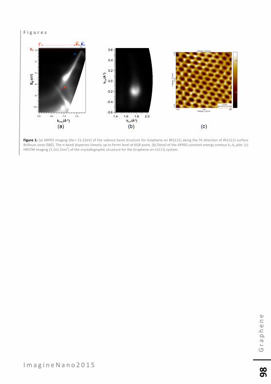
I m a g i n e N a n o 2 0 1 5
Gr
ap
he
ne
98
F i g u r e s
Figure 1: (a) ARPES imaging (He-I 21.22eV) of the valence band structure for Graphene on Rh(111) along the ΓΚ direction of Rh(111) surface Brillouin zone (SBZ). The π-band disperses linearly up to Fermi level at KGR point. (b) Detail of the APRES constant energy contour kx-ky plot. (c) HRSTM imaging (2.2x2.2nm2) of the crystallographic structure for the Graphene on Ir(111) system.

I m a g i n e N a n o 2 0 1 5
Gr
ap
he
ne
99
S t r o n g I n t e r a c t i o n b e t w e e n G r a p h e n e E d g e a n d M e t a l R e v e a l e d b y S c a n n i n g T u n n e l i n g M i c r o s c o p y 1Samsung Advanced Institute of Technology, Suwon 443-803, Korea, 2Department of Mechanical Engineering, Korea Advanced Institute of Science and Technology (KAIST), Daejeon 305-701, Korea
3 The interaction between a graphene edge and the underlying metal is investigated through the use of scanning tunneling microscopy (STM) and density functional theory (DFT) calculations and found to influence the geometrical structure of the graphene edge and its electronic properties [1]. STM study reveals that graphene nanoislands grow on a Pt(111) surface with the considerable bending of the graphene at the edge arising from the strong graphene-edge–Pt-substrate interactions. Periodic ripples along the graphene edge due to both the strong interaction and the lattice mismatch with the underlying metal were seen. DFT calculations confirm such significant bending and also reproduce the periodic ripples along the graphene edge. The highly distorted edge geometry causes strain-induced pseudo-magnetic fields, which are manifested as Landau levels in the scanning tunneling spectroscopy. The electronic properties of the graphene edge are thus concluded to be strongly influenced by the curvature rather than the localized states along the zigzag edge as was previously predicted. R e f e r e n c e s
[1] Kim, H. W. et al. Carbon, 78 (2014), 190.
F i g u r e s
Figure 1: STM of Graphene grown a Pt (111) substrate and side view of the graphene ribbon on the Pt model system by DFT calculation.
Hyo Won Kim1,
JiYeon Ku1, Wonhee Ko1, Insu Jeon1, Hyeokshin Kwon1, Seunghwa Ryu2, Se-Jong Kahng1,3, Sung-Hoon Lee1, Sung Woo Hwang1, and Hwansoo Suh1
I m a g i n e N a n o 2 0 1 5
Gr
ap
he
ne
10
0
M e s o e p i t a x y o f g r a p h e n e : c o n t i n u o u s f i l m f o r m a t i o n Department of Materials Science and Engineering, Seoul National University, Korea
Polycrystalline nature of graphene is a major issue to be overcame in real application of CVD graphene. Recently, liquid Cu was used as catalytic substrate for graphene growth, and due to liquid surface nature, self-assembly of graphene islands was observed. However, stitching of each graphene islands still need to be investigated since thermal stress may result cracks. We verified that typical growth conditions for self-assembly of graphene on liquid Cu are not adequate for obtaining continuous graphene film, due to low supersaturation ratio. Two-step growth method was suggested in order to reduce thermal induced cracks, and fill the narrow gaps between graphene islands. Also, the transport behavior was studied via Van der Pauw measurement of the graphene film, and TLM patterning of two adjacent graphene islands. Self-assembled graphene shows lower resistance compared to randomly grown graphene islands which are typically observed on solid Cu.
Seong-Yong Cho, Min-Sik Kim, Hyun-Mi Kim, Min-Su Kim, Ki-Ju Kim, Sang-Hoon Lee, and Ki-Bum Kim*

I m a g i n e N a n o 2 0 1 5
Gr
ap
he
ne
10
1
M o S 2 a n d d i c h a l c o g e n i d e b a s e d d e v i c e s a n d h y b r i d h e t e r o s t r u c t u r e s EPFL, Lausanne, Switzerland
MoS2 and transition metal dichalcogenides have opened numerous research directions and potential applications for this diverse family of nanomaterials. The combination of these 2D materials in heterostructures can result in a huge number of potentially interesting new materials. Most of the attention in this field is focused on heterostructures composed of different 2D materials. In my talk, I will present some of our recent efforts in this direction, oriented towards realizing combinations of 2D and 3D materials into van der Waals heterostructures. I will report on high-performance photodetectors based on 2D/3D heterostructures that can operate with internal gain and high sensitivity. Our devices also show very low noise, due to the unique architecture of the 2D/3D heterojunction. Next, I will give an update on our efforts to realize high-performance electrical circuits based on TMD materials.
Andras Kis

I m a g i n e N a n o 2 0 1 5
Gr
ap
he
ne
10
2
P h o t o d e t e c t i o n a n d n a n o - p h o t o n i c s o f g r a p h e n e a n d h e t e r o s t r u c t u r e s o f 2 d m a t e r i a l s The Institute of Photonics Sciences (Barcelona)
The interaction of light with graphene and heterostructures of related 2d materials embodies a wide variety of physical processes such as ultra-fast photoconversion, strong light-matter interactions and highly confined plasmons, with strong potential for disruptive opto-electronic technologies. In this talk, several examples of the ultra-fast opto-electronic and nano-photonic capabilities of novel 2d material heterostructures are being addressed. We argue that graphene encapsulated in hexagonal boron nitride (h-BN) is a material system with remarkable nano-photonic properties. First, we find that it is an excellent host for extremely strongly confined light with reduced plasmon losses. We identify experimentally and theoretically the main damping channels. Second, h-BN itself is an interesting optical material as it shows natural hyperbolic behaviour, meaning that the in- and out-of-plane component of the permittivity have opposite signs in the reststrahlen frequency bands. This implies that h-BN supports deep subwavelength slow-light phonon polariton modes within those bands. Combining h-BN with graphene gives rise to unconventional plasmon–phonon hybridization and this hybrid system can be used for tailoring novel subwavelength metama-terials. Next, we address recent photovoltage generation experiments with unprecented time resolution, applied to graphene and heterostructures of 2 materials. We control and study the underlying carrier-carrier interactions and charge carrier transfer dynamics.
R e f e r e n c e s
[1] Electrical Control of Optical Emitter Relaxation
Pathways enabled by Graphene. K.J. Tielrooij, L. Orona, A. Ferrier, M. Badioli, G. Navickaite, S. Coop, S. Nanot, B. Kalinic, T. Cesca, L. Gaudreau, Q. Ma, A. Centeno, A. Pesquera, A. Zurutuza, H. de Riedmatten, P. Goldner, F.J. García de Abajo, P. Jarillo-Herrero, F.H.L. Koppens Nature Physics [online DOI: 10.1038/nphys3204] (2015)
[2] Highly confined low-loss plasmons in
graphene–boron nitride heterostructures. A. Woessner, M. B. Lundeberg, Y. Gao, A. Principi, P. Alonso-González, M. Carrega, K. Watanabe, T. Taniguchi, G. Vignale, M. Polini, J. Hone, R. Hillenbrand, F. H. L. Koppens Nature Materials [online DOI: 10.1038/NMAT4169] (2014)
[3] Ultrafast electronic read-out of diamond NV
centers coupled to graphene. Andreas Brenneis, Louis Gaudreau, Max Seifert, Helmut Karl, Martin S. Brandt, Hans Huebl, Jose A. Garrido , Frank H.L. Koppens, Alexander W. Holleitner Nature Nanotechnoly [online DOI: 10.1038/nnano.2014.276] (2014)
[4] Hybrid 2D–0D MoS2–PbS Quantum Dot
Photodetectors. Kufer, Dominik, Ivan Nikitskiy, Tania Lasanta, Gabriele Navickaite, Frank HL Koppens, and Gerasimos Konstantatos Advanced Materials 27, no. 1, 176-180 (2015)
[5] Photodetectors based on graphene, other two-
dimensional materials and hybrid systems. F. H. L. Koppens, T. Mueller, Ph. Avouris, A. C. Ferrari, M. S. Vitiello, M. Polini Nature Nanotechnol. 9, 780-793 (2014)
[6] Phonon-mediated mid-infrared photoresponse
of graphene. M. Badioli , A. Woessner, K. J. Tielrooij, S. Nanot, G. Navickaite, T. Stauber, F. J. Garcia de Abajo, F. H. L. Koppens Nano Lett. 14, 6374–6381 (2014)
Frank Koppens
I m a g i n e N a n o 2 0 1 5
Gr
ap
he
ne
10
3
I n v e s t i g a t i o n o f e l e c t r o l y t e s f o r g r a p h e n e o p t i c a l m o d u l a t o r s Department of physics, Bilkent university, 06800, Ankara, Turkey
Notably, atomically thin 2 dimensional (2d) crystals provide new perspective for novel optoelectronic devices. Since the thickness of 2d crystals is much shorter than the wavelength of light, their response originates from the free charge carriers. Recently graphene provides new opportunities for optoelectronic devices. Ability to tune the free carrier on graphene through electrostatic doping, enables to control optical absorption in a very broad spectrum. Controlling optical properties in the visible spectra, however, remains as a challenge due to requirements of very large charge densities in the order of 1014 cm-2. Recently [1] we discovered a very simple device structure to control optical properties of graphene using a supercapacitor structure (Figure 1a). In this device architecture, we used two graphene electrodes and electrolyte medium. Application of a voltage bias polarized the electrolyte and yield large shift in the Fermi energy in the order of 1.5 eV with corresponding charge densities of 1014cm-2. The electrical and chemical properties of the electrolyte are the key parameters that define the performance of these optical modulators. In this report, we will talk about our investigation of various organic electrolytes (EL) for graphene optical modulators: liquid EL - PC/LiBOB (propylene carbonate/lithium bis(oxalato)borate), gel EL - PVA/LiBOB (polyvinyl alcohol/lithium bis(oxalato)borate) and solid EL - p(VDF-HFP)/IL (poly (vinylidene fluoride-co-hexafluoropropylene) fluoroelastomer/ionic liquid). Thereby, based on electrical and optical results we have established higher capacitance at 78 μF in the case of a gel EL, using during the changing of the transmission versus the wavelength for various
bias voltages. Also, we have found the increasing of transmission at 3 times for solid EL (Figure 1b) in comparison with liquid and gel Els and have detected the possibilities of gel EL to work in negative region. Analyzing obtained results we suggest the best and most suitable solid EL for fabrication graphene-based SC devices permitting to increase the modulation efficiencies by increasing the interaction of light with graphene electrodes. We anticipate that using namely of solid EL, except getting the desired electro-optical properties, will allow us to minimize the size of the SC and to vary the its form. R e f e r e n c e s
[1] E.O. Polat and C. Kocabas, Nano Lett, 13
(2013) 5851−5857.
Evgeniya Kovalska
and Coskun Kocabas
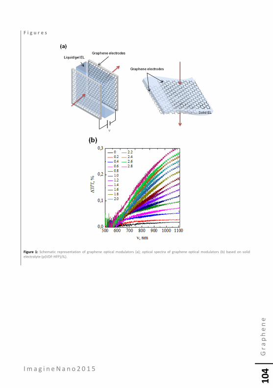
I m a g i n e N a n o 2 0 1 5
Gr
ap
he
ne
10
4
F i g u r e s
Figure 1: Schematic representation of graphene optical modulators (a); optical spectra of graphene optical modulators (b) based on solid electrolyte (p(VDF-HFP)/IL).

I m a g i n e N a n o 2 0 1 5
Gr
ap
he
ne
10
5
R e d u c e d g r a p h e n e o x i d e b a s e d n a n o c o m p o s i t e f i l m s f o r e n h a n c e d e l e c t r o c h r o m i c p e r f o r m a n c e University of Turku, Turku University Centre for Materials and Surfaces (MATSURF), Laboratory of Materials Chemistry and Chemical Analysis, Vatselankatu 2, FIN-20014 Turku, Finland
Reduced graphene oxide has been investigated [1,2] and applied as component in polymer composites. Polyviologen (PV)-reduced graphene oxide (rGO) nanocomposite films were fabricated by simple, onestep reductive electropolymerization of cyanopyridinium based precursor monomer (CNP) in an aqueous dispersion of graphene oxide (GO). Since the polymer formation and reduction of graphene oxide occurs within the same potential window, electrocodeposition method was preferred for obtaining nanostructured PV-rGO films. Cyclic voltammetry experiments of PV-rGO displayed two well resolved, reversible one-electron redox processes typical of viologen. Being a redox polymer, incorporation of rGO further enhances the electroactivity of the PV in the composite films. Vibrational spectral analysis with surface characterization revealed structural changes after composite formation along with subsequent reduction of GO within the polymer matrix. The PV-rGO nanostructured film exhibits a highcontrast electrochromism with low driving voltage induced striking color changes from transparent (0 V) to purple (-0.6 V), high coloration efficiency, fast response times and better cycling stability compared to a pristine PV film [3,4]. This performance can be attributed to the high stability of the electrochrome in the composite assembly induced by electrostatically driven non-covalent interactions between redox PV2+ and negatively charged rGO, improved electrical conductivity and enlarged surface area accessed through reinforced nanostructured graphene sheets for tethering PV molecules.
R e f e r e n c e s
[1] Jussi Kauppila, Peter Kunnas, Pia Damlin,
Antti Viinikanoja, Carita Kvarnströms. Electrochim. Acta. 89 (2013) 84
[2] A. Viinikanoja, X. Wang, J. Kauppila, C. Kvarnström, Phys. Chem. Chem. Phys. 14 (2012) 14003.
[3] Gadgil B, Damlin P, Ääritalo T, Kankare J, Kvarnström C. Electrochim Acta 97 (2013) 378-85.
[4] Gadgil B, Damlin P, Ääritalo T, Kvarnström C. Electrochim Acta 133 (2014) 268-74.
F i g u r e s
Figure 1: Changes in the UV-vis absorption spectra for bleached state (0 V) and colored state (-0.6 V) for PV (blue line) and PV-rGO (red line) films with 0.1 M KCl in water.
Bhushan Gadgil, Pia Damlin and Carita Kvarnström

I m a g i n e N a n o 2 0 1 5
Gr
ap
he
ne
10
6
E p i t a x i a l G r o w t h o f S i n g l e - d o m a i n H e x a g o n a l B o r o n N i t r i d e 1Elettra-Sincrotrone Trieste S.C.p.A., AREA Science Park, S.S. 14 km 163.5, 34149 Trieste, Italy 2Physics Department and CENMAT, University of Trieste, Via Valerio 2, 34127 Trieste, Italy 3National Institute of Materials Physics, Atomistilor 105b, 077125 Magurele-Ilfov, Romania 4CNR-Institute for Complex Systems, Via Fosso del Cavaliere 100, 00133 Roma, Italy 5IOM-CNR, Laboratorio TASC, AREA Science Park, S.S. 14 km 163.5, 34149 Trieste, Italy
3d printing is a rapidly growing field. It consists in The rising interest of the scientific community in graphene (GR), motivated by its fascinating properties and wide range of potential applications, has triggered substantial interest also on other twodimensional (2D) atomic crystals and, in particular, on hexagonal boron nitride (h-BN) [1], which provides a superior insulating platform for high-performance GR devices [2]. However, a number of challenges still awaits the scientific community before the full potential of 2D atomic crystals can be exploited, such as the development of reliable methods for the growth of high-quality GR and h-BN single layers. For instance, it is still challenging to obtain large h-BN single crystalline domains because of the formation of rotated phases that give rise to grain boundaries and other 1D defects [3,4]. A deeper understanding of the h-BN growth mechanism is therefore highly desirable in order to find the optimum approach to grow high-quality films. Here, we investigate the structure of h-BN grown on Ir(111) by chemical vapor deposition (CVD) of borazine [5]. Using synchrotron radiation photoelectron spectroscopy, photoelectron diffraction and low energy electron diffraction we show that hightemperature borazine deposition gives rise to a h-BN monolayer formed by domains with opposite orientation, while a h-BN monolayer with single orientation can be synthesized by dosing borazine at room temperature and subsequently annealing the sample [6]. Our results provide new insight into the strategies for producing h -BN monolayers with single orientation.
R e f e r e n c e s
[1] M. Corso et al., Science, 303 (2004) 217. [2] C. R. Dean et al., Nature Nanotechnology, 5
(2010) 722. [3] W. Auwärter et al., Surface Science, 545
(2003) L735. [4] G. Dong et al., Physical Review Letters, 104
(2010) 096102. [5] F. Orlando et al., Journal of Physical
Chemistry C, 115 (2012) 157. [6] F. Orlando et al., ACS Nano, DOI:
10.1021/nn5058968 (2014) in print.
Paolo Lacovig1,
Fabrizio Orlando2, Luca Omiciuolo2, Nicoleta G. Apostol1,3, Rosanna Larciprete4, Alessandro Baraldi2,5, and Silvano Lizzit 1

I m a g i n e N a n o 2 0 1 5
Gr
ap
he
ne
10
7
N i t r o g e n d o p i n g o f g r a p h e n e s t u d i e d b y s c a n n i n g t u n n e l i n g m i c r o s c o p y 1Laboratoire Matériaux et Phénomènes Quantiques, Université Paris diderot 10 rue Alice Domon et Léonie duquet, Paris France 2Research Center in Physics of Matter and Radiation, Université de Namur, 61 Rue de Bruxelles, 5000 Namur, Belgium 3Laboratoire d'Etude des Microstructures, ONERA-CNRS, 92322 Châtillon Cedex, France
Tuning the electronic properties of graphene is a key to the development of carbon-based electronics or other applications taking advantages of the properties of this 2D-material. Among the possible strategies to achieve this goal, the insertion of nitrogen atoms in the carbon lattice appears to be particularly interesting as it allows to perform regular doping with minimal atomic relaxation. Several studies have focused on the properties of nitrogen doped graphene down to the atomic scale using scanning tunneling microscopy (STM). Here we report on the systematic investigation of nitrogen doped graphene on SiC(000-1) using STM and scanning tunneling spectroscopy (STS). The spectroscopic measurements show that the doping induces a shift of the Dirac point that does not follow the expected behavior from a rigid band model. This point will be discussed. In addition to single substituted nitrogen the inserted atoms can have different local environments: pyridinic where the nitrogen is combined with a vacancy, and pairs of nitrogen with different interatomic distances (see figure). The isolated single nitrogen atoms have been found to be the most common characterized by a localized resonance in valence band [1]. On nitrogen pairs, the local density of states is different from that of single graphitic nitrogen suggesting that an electronic interaction occurs between N atoms even when they are separated by several atomic sites. The properties of these complex atomic configurations will be shown and discussed. The extensive measure by STM/STS of N-doped graphene allow to provide a detailed background
to better understand the electronic properties of chemically doped graphene. R e f e r e n c e s
[1] F. Joucken et al., Phys; rev. B, 85 (2012)
161408 (R). F i g u r e s
Figure 1: STM image of nitrogen doped graphene revealing different atomic configurations of the doping sites. Local spectroscopy showing the difference between spectra measured on different types of doping sites.
J. Lagoute1,
F. Joucken2, Y. Tison1, V. Repain1, C. Chacon1, Y. Girard1, A. Bellec1, H. Amara3, F. Ducastelle3, L. Henrard2, R. Sporken2, S. Rousset1
I m a g i n e N a n o 2 0 1 5
Gr
ap
he
ne
10
8
F r o m s i n g l e t o m u l t i l a y e r g e r m a n e n e Aix-Marseille University, CNRS-PIIIM, Campus de St Jérôme, F-13297 Marseille Cedex, France, Instituto de Ciencia de Materiales de Madrid, ICMM-CSIC, C/Sor Juana Inés de la Cruz, 3 Cantoblanco, 28049 Madrid, Spain
There is a surge of works on new artificial elemental honeycomb two-dimensional materials beyond graphene, especially silicene sheets, first synthesized in 2012 on Ag(111) substrates [1], and germanene single layer ones, epitaxially grown, just very recently in 2014, on a Au(111) template [2]. The amazingly fast fabrication of a Room Temperature silicene Field Effect Transistor [3] will surely give a strong boost to research on these novel synthetic 2D materials, which do not exist in nature and which are, per se, directly compatible with the ubiquitous Si-based microelectronics processes. Here, we will present further advances on germanene, possibly a 2D topological insulator robust up to nearly RT, upon reporting novel results acquired by STM and Synchrotron Radiation PhotoElectron Spectroscopy on multilayer germanene sheets [4]. R e f e r e n c e s
[1] P. Vogt et al., Phys. Rev. Lett., 108 (2012)
155501. [2] M. E. Dávila, L. Xian, S. Cahangirov, A. Rubio
and G. Le Lay, New J. Phys., 16 (2014) 095002.
[3] L. Tao et al., Nature Nanotechnol., in press. [4] M.E. Dávila and G. Le Lay, to be published.
Guy Le Lay, Maria Eugenia Dávila

I m a g i n e N a n o 2 0 1 5
Gr
ap
he
ne
10
9
T o w a r d s l a r g e - a r e a m o n o c r y s t a l l i n e g r a p h e n e : S y n t h e s i s a n d a p p l i c a t i o n s 1Center for Integrated Nanostructure Physics, Institute for Basic Science, Sungkyunkwan University,Suwon, Kyunggi-do 440-746, South Korea 2Department of Energy Science, Department of Physics, Sungkyunkwan University,Suwon, Kyunggi-do 440-746, South Korea
Grain boundaries in graphene are formed via the stitching of islands during the initial growth stage, and these boundaries govern transport properties and related device performance. Graphene can be ideally grown from a single nucleation seed, but its growth to large-area graphene can be terminated by several unknown self-limiting growth factors. Another approach is to start with numerous nucleation seeds and allow them to grow and coalesce together to produce large-area graphene. However, graphene grain boundaries (GGBs) are inevitably formed via stitching of graphene flakes, consequently limiting the graphene quality. We will describe several growth factors to achieve monocrystalline graphene growth during CVD. In addition, we will also describe how the grain boundaries can be modified by functional groups and influence transport properties at the grain boundaries. In addition, applications to electronics and energy storage done recently in our laboratory will be discussed further.
Young Hee Lee

I m a g i n e N a n o 2 0 1 5
Gr
ap
he
ne
11
0
C u r r e n t R e s e a r c h S t a t u s o f K o r e a o n G r a p h e n e & C a r b o n N a n o t u b e s 1IBS Center for Integrated Nanostructure Physics, Institute for Basic Science, Sungkyunkwan University, Suwon 440-746, Republic of Korea. 2Department of Energy Science, Department of Physics, Sungkyunkwan University, Suwon 440-746,Republic of Korea.
Nanoscience and nanotechnology have been considered to be one of the most important sciences and technologies for electronics, energy storage and production, and biological and medical applications to drive future industries of Korea. Therefore, Korean Government set the Integral Development Plan for Nanotechnology, for the first time in 2001, which has been modified and enhanced every 5 years, taking the change in technologies and industrial environments into consideration. Since Korean Government started supporting the research on nanotechnology with these plans, about $ 3.138 billion have been invested in it for 13 years. Among the amount, $ 2.485 billion (79.2%) were supplied for research and development, and $ 493 billion (15.7%) and $ 160 billion (5.1%) were provided to build the infrastructures and to foster manpower, respectively. It is quite meaningful for us to look into the research progress of carbon nanomaterials, such as carbon nanotubes and graphene, which have played a main role in promoting the early nanoscience of Korea, because we can speculate how Korean nanoscience is structured, which can predict change in the future nanoscience by analyzing funds and publications.
Young Hee Lee1,2
I m a g i n e N a n o 2 0 1 5
Gr
ap
he
ne
11
1
G r a p h e n e S t a n d a r d s : B u i l d i n g a B i g g e r B u s i n e s s National Electrical Manufacturers Association (NEMA) 1300 North 17th Street, Suite 900 Rosslyn, Virginia 22209, USA
Electrotechnical products, from the standpoint of their individual components, function as a system. For example, today’s smart phones offer unprecedented functionality in our everyday lives, but this made possible only by integrating of different technologies, like the software, the luminescent materials, the touch screen or the audio capabilities, into a system through standardization. Standards are at the core of not only every end use product, but to each of the components of that product because these components must perform adequately to work together. However the graphene industry is faced with a worldwide challenge – gaining the trust of its customers. Claims about performance and characteristics do not currently have the standardized requirements and measurement techniques behind them in place to give customers confidence that the bottle of graphene they bought indeed contains what the supplier claims is in there, and that it will do what it’s supposed to, will do it reliably, and do it reliability for a long time. Graphene suppliers can solve this dilemma by developing standards will help facilitate this over the long-term because they create a baseline for expanding markets and building new solutions. This starts at the basic level of making sure suppliers and customers are speaking the same language in terms of vocabulary, measurements, and test procedures. This can only be accomplished by working together to create value for the customer.
Mike Leibowitz
I m a g i n e N a n o 2 0 1 5
Gr
ap
he
ne
11
2
H i g h S e n s i t i v i t y o f G r a p h e n e - b a s e d S e n s o r s – O p p o r t u n i t i e s a n d L i m i t a t i o n s University of Siegen, Department of Electrical Engineering and Computer Science, Siegen,Germany
The two-dimensional nature of graphene leads to an extremely high surface-to-volume ratio, which promises ultrahigh sensitivity of graphene-based sensors [1]. The ultimate thinness and high Young’s modulus of graphene may be utilized in membrane-based devices with very high resonant frequencies for mass sensing applications [2]. In combination with an impressive stretchability, this may further lead to applications as piezoresistive graphene membrane-based sensors [3]. While the fundamental properties of graphene apparently make it an ideal candidate for such applications, in reality one has to deal with a number of parasitic effects that can influence and falsify the response of a graphene sensor. This talk aims to carefully balance the discussion about the merits and disadvantages of graphenebased sensors based on experimental data. R e f e r e n c e s
[1] F. Schedin, A. K. Geim, S. V. Morozov, E. W.
Hill, P. Blake, M. I. Katsnelson, and K. S. Novoselov, “Detection of individual gas molecules adsorbed on graphene,” Nat Mater, vol. 6, pp. 652–655, 2007.
[2] T. Mashoff, M. Pratzer, V. Geringer, T. J. Echtermeyer, M. C. Lemme, M. Liebmann, and M. Morgenstern, “Bistability and Oscillatory Motion of Natural Nanomembranes Appearing within Monolayer Graphene on Silicon Dioxide,” Nano Lett., vol. 10, pp. 461–465, 2010.
[3] A. D. Smith, F. Niklaus, A. Paussa, S. Vaziri, A. C. Fischer, M. Sterner, F. Forsberg, A. Delin, D. Esseni, P. Palestri, M. Östling, and M. C. Lemme, “Electromechanical Piezoresistive
Sensing in Suspended Graphene Membranes,” Nano Lett., vol. 13, no. 7, pp. 3237–3242, Jul. 2013.
Max C. Lemme

I m a g i n e N a n o 2 0 1 5
Gr
ap
he
ne
11
3
P r i n t e d M o S 2 / G r a p h e n e P h o t o d e t e c t o r Cambridge Graphene Centre, 9 JJ Thomson Avenue Cambridge CB3 0FA, UK
The electrical and optical properties of graphene and other 2d crystals are ideal for flexible, transparent, conductive electrodes [1], thin film transistors (TFTs) [2], photodetectors (PDs) [3], flexible batteries and smart textiles [2]. Liquid phase exfoliation (LPE) allows one to produce printable inks [4, 5] based on graphene and 2d crystals. LPE can be used to control concentration and morphology of 2d flakes at room temperature in a wide range of solvents [6, 7]. Inkjet-printed graphene/MoS2 PDs were reported with an external responsivity of few tens of nA/W at drain voltage of 40V [8]. Here we report a graphene/MoS2 PD, Fig.1 (a) fabricated by inkjet-printing on polyethylene terephthalate (PET) a 40μm MoS2 channel and then contacted by two inkjet printed graphene electrodes. In this configuration, graphene acts as conductive electrode, while MoS2 is the active layer where light absorption takes place. The device has an external responsivity of 960 nA/W, measured at 514nm and drain voltage of 30V, Fig.1 (b). This is 2 orders of magnitude higher than the previous reports [8]. Our device has an internal responsivity up to 0.2mA/W. This result demonstrates the viability of inkjet printed 2d-material inks for PDs, suitable for flexible, printed optoelectronics. R e f e r e n c e s
[1] F. Bonaccorso et al., Nat. Photon., 4 (2010)
611. [2] A.C. Ferrari et al., Nanoscale, DOI:
10.1039/c4nr01600a, (2014). [3] F.H.L. Koppens et al., Nat. Nanotec., 10
(2014) 780. [4] F. Torrisi et al., ACS Nano, 6 (2012) 4.
[5] F. Torrisi et al., Nat. Nanotec., 10 (2014) 738. [6] J.N. Coleman et al., Science, 331 (2011) 568. [7] Y. Hernandez et al., Nat. Nanotec., 3 (2008)
563. [8] J. Finn et al., J. Mater. Chem. C, 2 (2014) 925. F i g u r e s
Figure 1: a) Printed graphene/MoS2 photodetector. b) Time domain photoresponse of the graphene/MoS2 photodetector measured at 514nm and at +30V bias voltage.
L. Lombardi, F.Torrisi, F.Tomarchio and A. C. Ferrari
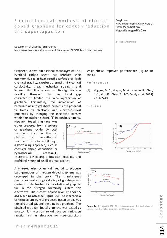
I m a g i n e N a n o 2 0 1 5
Gr
ap
he
ne
11
4
E l e c t r o c h e m i c a l s y n t h e s i s o f n i t r o g e n d o p e d g r a p h e n e f o r o x y g e n r e d u c t i o n a n d s u p e r c a p a c i t o r s Department of Chemical Engineering Norwegian University of Science and Technology, N-7491 Trondheim, Norway
Graphene, a two dimensional monolayer of sp2-hybrided carbon sheet, has received wide attention due to its huge specific surface area, high chemical stability, excellent thermal and electrical conductivity, great mechanical strength, and inherent flexibility as well as ultrahigh electron mobility. However, the zero band gap characteristic limited the wide application of graphene. Fortunately, the introduction of heteroatoms into graphene presents the potential to tweak its electronic and electrochemical properties by changing the electronic density within the graphene sheet. [1] In previous reports, nitrogen doped graphene was either prepared from graphene or graphene oxide by post treatment, such as thermal, plasma, or hydrothermal treatment, or obtained through a bottom up approach, such as chemical vapor deposition or hydrothermal process.[1] Therefore, developing a low-cost, scalable, and ecofriendly method is still of great interest. A one-step electrochemical method to produce bulk quantities of nitrogen doped graphene was developed in this work. The simultaneous production and nitrogen doping of graphene was realized by electrochemical exfoliation of graphite foil in the nitrogen containing sulfate salt electrolyte. The highest doping level of about 5 at% N can be achieved (Figure 1A). The mechanism of nitrogen doping was proposed based on analysis the exhausted gas and the obtained graphene. The obtained nitrogen doped graphene was tested as catalyst for electrochemical oxygen reduction reaction and as electrode for supercapacitors
which shows improved performance (Figure 1B and C). R e f e r e n c e s
[1] Higgins, D. C.; Hoque, M. A.; Hassan, F.; Choi,
J.-Y.; Kim, B.; Chen, Z., ACS Catalysis, 4 (2014) 2734-2740.
F i g u r e s
Figure 1: XPS spectra (A), RDE measurements (B), and electron transfer number (C) of Graphene and NGraphene.
Fengliu Lou, Navaneethan Muthuswamy, Marthe Emelie Melandsø Buana, Magnus Rønning and De Chen

I m a g i n e N a n o 2 0 1 5
Gr
ap
he
ne
11
5
S y n t h e s i s , C h a r a c t e r i z a t i o n a n d E n g i n e e r i n g o f T w o - D i m e n s i o n a l M a t e r i a l s Department of Materials Science and NanoEngineering Rice University, Houston, TX 77005, USA
In this talk, we first report the controlled vapor phase synthesis of transition metal dichalcogenide atomic layers and their heterostructures. The atomic structure and morphology of the grains and their boundaries are examined and first-principles calculations are applied to investigate their energy landscape. More importantly, if precise two-dimensional domains of metallic, semiconducting and insulating atomic layers can be seamlessly stitched together, in-plane heterostructures with interesting electronic applications could potentially be created. Here, we show that planar graphene/h-BN/h-BNC heterostructures can be formed either by growing graphene in lithographically-patterned h-BN atomic layers or by a direct chemical conversion process. Next, we report the in situ tensile testing of suspended graphene using a nanomechanical device to measure the fracture toughness of graphene. Our combined experiment and modeling verify the applicability of the classic Griffith theory of brittle fracture to graphene. The implications of the effects of defects such as grain boundaries on mechanical and electrical properties of two-dimensional atomic layers will also be discussed. Finally, we demonstrate how self-assembled monolayers with a variety of end termination chemistries can be utilized to tailor the physical properties of single-crystalline MoS2 atomic-layers. Our data suggests that combined interface-related effects of charge transfer, built-in molecular polarities, varied densities of defects, and remote interfacial phonons strongly modify the electrical and optical properties of MoS2, illustrating an engineering approach for local and universal property modulations in two-dimensional atomic-layers.
Jun Lou
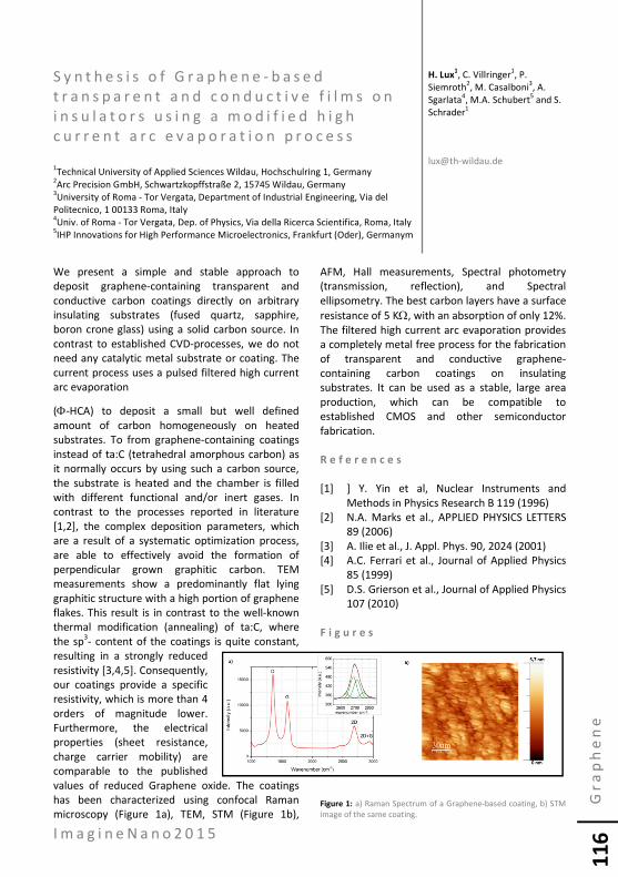
I m a g i n e N a n o 2 0 1 5
Gr
ap
he
ne
11
6
S y n t h e s i s o f G r a p h e n e - b a s e d t r a n s p a r e n t a n d c o n d u c t i v e f i l m s o n i n s u l a t o r s u s i n g a m o d i f i e d h i g h c u r r e n t a r c e v a p o r a t i o n p r o c e s s 1Technical University of Applied Sciences Wildau, Hochschulring 1, Germany 2Arc Precision GmbH, Schwartzkopffstraße 2, 15745 Wildau, Germany 3University of Roma - Tor Vergata, Department of Industrial Engineering, Via del Politecnico, 1 00133 Roma, Italy 4Univ. of Roma - Tor Vergata, Dep. of Physics, Via della Ricerca Scientifica, Roma, Italy 5IHP Innovations for High Performance Microelectronics, Frankfurt (Oder), Germanym
We present a simple and stable approach to deposit graphene-containing transparent and conductive carbon coatings directly on arbitrary insulating substrates (fused quartz, sapphire, boron crone glass) using a solid carbon source. In contrast to established CVD-processes, we do not need any catalytic metal substrate or coating. The current process uses a pulsed filtered high current arc evaporation
(Φ-HCA) to deposit a small but well defined amount of carbon homogeneously on heated substrates. To from graphene-containing coatings instead of ta:C (tetrahedral amorphous carbon) as it normally occurs by using such a carbon source, the substrate is heated and the chamber is filled with different functional and/or inert gases. In contrast to the processes reported in literature [1,2], the complex deposition parameters, which are a result of a systematic optimization process, are able to effectively avoid the formation of perpendicular grown graphitic carbon. TEM measurements show a predominantly flat lying graphitic structure with a high portion of graphene flakes. This result is in contrast to the well-known thermal modification (annealing) of ta:C, where the sp3- content of the coatings is quite constant, resulting in a strongly reduced resistivity [3,4,5]. Consequently, our coatings provide a specific resistivity, which is more than 4 orders of magnitude lower. Furthermore, the electrical properties (sheet resistance, charge carrier mobility) are comparable to the published values of reduced Graphene oxide. The coatings has been characterized using confocal Raman microscopy (Figure 1a), TEM, STM (Figure 1b),
AFM, Hall measurements, Spectral photometry (transmission, reflection), and Spectral ellipsometry. The best carbon layers have a surface resistance of 5 KΩ, with an absorption of only 12%. The filtered high current arc evaporation provides a completely metal free process for the fabrication of transparent and conductive graphene-containing carbon coatings on insulating substrates. It can be used as a stable, large area production, which can be compatible to established CMOS and other semiconductor fabrication. R e f e r e n c e s
[1] ] Y. Yin et al, Nuclear Instruments and
Methods in Physics Research B 119 (1996) [2] N.A. Marks et al., APPLIED PHYSICS LETTERS
89 (2006) [3] A. Ilie et al., J. Appl. Phys. 90, 2024 (2001) [4] A.C. Ferrari et al., Journal of Applied Physics
85 (1999) [5] D.S. Grierson et al., Journal of Applied Physics
107 (2010) F i g u r e s
Figure 1: a) Raman Spectrum of a Graphene-based coating, b) STM image of the same coating.
H. Lux1, C. Villringer1, P.
Siemroth2, M. Casalboni3, A. Sgarlata4, M.A. Schubert5 and S. Schrader1

I m a g i n e N a n o 2 0 1 5
Gr
ap
he
ne
11
7
G r a p h e n e n a n o p o r o u s n e t w o r k : f r o m s y n t h e s i s t o e l e c t r o n i c s t r u c t u r e c a l c u l a t i o n s 1University of Grenoble Alpes, Institut Néel, F-38042 Grenoble, France 2CNRS, Institut Néel, F38042 Grenoble, France 3Institut FEMTO-ST, Université de France-Comté, CNRS, ENSMM, 32 Avenue de l'Observatoire, F-25044 Besançon, France
The family of two-dimensional materials is a rapidly growing one that emerged with graphene synthesis ten years ago. Tailoring the structure of these materials allows engineering their properties. One example is the change in the topology of graphene band structure as a function of the number of layer and their stacking. [1] Porous versions of graphene such as antidot lattice [2] (GAL) offer new degrees of freedom for structure-engineering of the properties: gap opening, anisotropic renormalization of Dirac velocity, spin qubit.... Up to now, experimental realization of GAL are mostly based on top-down approach and relied on lithography performed on graphene sheets. [3] We report here a convergent surface polymerization reaction scheme on Au(111), based on a triple aldol condensation, yielding a purely carbon, covalent nanoporous two-dimensional network whose formation and structure are studied with scanning tunneling microscopy. [4] Ab initio calculations including van der Waals interactions have been performed on the free standing network as well as on the network on Au(111) to analyse the role of the substrate in the convergent reaction. The electronic structure of the free standing network shows Kagome lattice like features: flat band and bands with linear dispersion together with a wide band gap. The possibility to enhance spin-orbit coupling in the system and then to turn it into a topological insulator will be discussed.
R e f e r e n c e s
[1] Ohta, T.; Bostwick, A.; McChesney, J. L.;
Seyller, T.; Horn, K.; Rotenberg, E. Phys. Rev. Lett. 98 (2007) 206802
[2] Pedersen, T. G.; Flindt, C.; Pedersen, J.; Mortensen, N. A.; Jauho, A. P.; Pedersen, K. Phys. Rev. Lett. 100 (2008) 136804
[3] Bai, J. W.; Zhong, X.; Jiang, S.; Huang, Y.; Duan, X. F. Nat. Nanotechnol. 5 (2010) 190.
[4] Landers, J.; Coraux, J; De Santis, Maurizio; Bendiab, N.; Lamare, Simon.; Magaud, L.; Cherioux, F., 2D Materials 1 (2014) 034005
F i g u r e s
Figure 1: :(Left) Scanning tunnel microscopy (STM) image of a fully conjugated carbon network synthesized on Au(111). (Right) Density functional theory (DFT) calculations showing the stable structure on Au(111). Middle inset shows the reaction based on a novel convergent approach via a triple aldolisation.
Magaud1,2
, Laurence, Landers1,2, John; Coraux1,2, Johann; Hallal, Ali 1,2;De Santis1,2, Maurizio; Bendiab Nedjma1,2; Lamare, Simon3; Cherioux3, Frédéric

I m a g i n e N a n o 2 0 1 5
Gr
ap
he
ne
11
8
E x c i t o n K i n e t i c s i n M o S 2 , M o S e 2 a n d W S e 2 m o n o l a y e r s 1Université de Toulouse, INSA-CNRS-UPS, LPCNO, 135 Avenue de Rangueil, 31077 Toulouse, France 2Ioffe Physical-Technical Institute of the RAS, 194021 St. Petersburg, Russia 3Beijing National Laboratory for Condensed Matter Physics, Institute of Physics, Beijing 100190, China
We have investigated the optical and valley properties for both neutral and charged exciton in transition metal dichalcogenide monolayers (ML): MoS2, MoSe2 and WSe2. In WSe2 MLs, we have combined linear and non-linear optical spectroscopy (one and two-photons PLE, Second Harmonic Generation spectroscopy) in order to evidence the neutral exciton excited states. The clear identification of exciton excited states combined with first principle calculations allows us to determine an exciton binding energy of the order of 600 meV. The deviation of the excited exciton spectrum from the standard Rydberg series will be discussed. Moreover we show that exciton valley coherence can be achieved following one or two-photons excitation [1]. The neutral and charged exciton dynamics have been measured by time-resolved photoluminescence and pump-probe Kerr rotation dynamics [2,3]. The neutral exciton valley depolarization is about 6 ps, a fast relaxation time resulting from the strong electron-hole Coulomb exchange interaction in bright excitons [4]. Its temperature dependence is well explained by the developed theory, taking into account the long-range Coulomb exchange interaction [5]. In contrast the valley polarization decay time for the charged exciton is much longer (~1ns). The large neutral exciton valley polarization induced by polarized light measured in stationary conditions is mainly explained by the very short recombination time [3, 6].
Finally we will compare the exciton dynamics in WSe2 mono and bi-layers [7]. R e f e r e n c e s
[1] G. Wang et al, arXiv:1404.0056 (2014) [2] G. Wang et al, Phys. Rev. B 90, 075413 (2014) [3] D. Lagarde et al, Phys. Rev. Lett 112, 047401
(2014) [4] C.R. Zhu et al, Phys. Rev.B 90, 161302(R)
(2014) [5] M. Glazov et al, Phys. Rev. B 89, 201302(R)
(2014) [6] G. Sallen, Phys. Rev. B 86, 081301(R) (2012) [7] G. Wang et al, Applied Phys. Lett. 105,
182105 (2014)
NG. Wang1 , L. Bouet1 , D. Lagarde1 , I. Gerber1, M. Glazov2, A. Balocchi1 , T. Amand1 , B.L. Liu3, B. Urbaszek1 and X. Marie
1

I m a g i n e N a n o 2 0 1 5
Gr
ap
he
ne
119
I n f r a r e d s p e c t r o s c o p y w i t h t u n a b l e g r a p h e n e p l a s m o n s : a n o v e l r o u t e f o r m o l e c u l a r s e n s i n g 1ICFO-Institut de Ciencies Fotoniques, Mediterranean Technology Park, 08860 Castelldefels, Barcelona, Spain 2ICREA-Institució Catalana de Recerca i Estudis Avançats, Passeig Lluís Companys, 23, 08010 Barcelona, Spain Infrared spectroscopy is an important field of research as it enables sensing of molecules through the measurement of their resonances, acting as molecular fingerprints. Nanophotonics is tightly bound to this field of research as the engineering of nano-scaled plasmonic structures is crucial for enhancing the local electromagnetic field. The high local field is mainly responsible for the giant surface-induced enhancement of infrared absorption (SEIRA) and Raman scattering (SERS) by molecules in close proximity of metallic nanoparticles. These techniques have brought a number of viable, cheap and efficient commercial applications, e.g., pregnancy tests based on metal colloids [1], and promise further revolutionary applications in plasmonic sensing, although they suffer from some drawbacks. Indeed, plasmon resonances in metal-based nanoparticles are fixed by the underpinning geometric details of the plasmonic structure and lack of efficient external tunability. Besides, their spectral width can not cover the whole broad spectrum of roto-vibrational infrared transitions, and thus they enhance only few molecular resonances. Multi-frequency sensors based on subwavelength hole arrays and optical antennas have been proposed for overcoming this limitation and for achieving broadband surface-enhanced spectroscopy [2, 3]. In the last years, doped graphene has emerged as an attractive alternative to noble metals for the exploitation of surface plasmons at infrared (IR) and terahertz (THz) frequencies. Here, we develop a theoretical framework accounting for SEIRA and SERS by molecules adsorbed on graphene nano-disks. We evaluate the efficiency of these graphene-based infrared sensors finding that, thanks to the outstanding tunability of graphene through externally applied gate voltage, broadband SEIRA and SERS can be achieved. The
calculated enhancement factors with respect to molecular cross-sections in the gas-phase (in the absence of graphene), are of the order of 103 for SEIRA and 104 for SERS, thus making these techniques highly appealing for sensing devices. R e f e r e n c e s [1] M. I. Stockman, Phys. Today 64, 39 (2011). [2] O. Limaj et al., J. Phys. Chem. C 117, 19119
(2013). [3] H. Aouani et al., ACS Nano 7, 669 (2013). F i g u r e s
Figure 1: (a) Sketch of the structure analyzed in this work, i.e. a graphene nano-disk of diameter D = 300nm surrounded by pyridine molecules at the coordinates R,h. (b) Absorption cross-section spectrum of the doped graphene nanodisk in the local-RPA limit with EF = 0.4eV. Insets depict the position-dependent induced-field amplitudes and the radial profiles of the induced charge density at the three resonant photon energies ℏω1 = 0.10eV, ℏω2 = 0.19eV, ℏω3 = 0.22eV where surface plasmon modes are excited. (c) Spectral change in the extinction cross-section induced by a single pyridine molecule placed at R = 0, h = 1nm. Labels A, B indicate the two leading absorption lines of pyridine. (d,e) Extinction cross-section map as a function of the molecule position in the x-z plane for (d) EF = 0.34eV, Ephot = 0.087eV, and (e) EF = 0.38eV, Ephot = 0.092eV.
Andrea Marini1, Iván Silveiro1 and F.
Javier García de Abajo1,2

I m a g i n e N a n o 2 0 1 5
Gr
ap
he
ne
120
E n h a n c e d T h e r m a l C o n d u c t i v i t y o f s i l v e r f i l l e d - e p o x y r e s i n l o a d e d w i t h C a r b o n N a n o t u b e s a n d G r a p h e n e 1 CNR-IPCF, Viale F. Stagno D’Alcontres 37, 98158 Messina, Italy 2 CNR-ISMN, Area della Ricerca RM1-Montelibretti, 00016 Monterotondo Scalo, Rome, Italy 3 Selex ES Via Villagrazia 79 90125 Palermo, Italy
The development of property-designed conductive adhesives represents an important technological step in the development of smart packaging systems for next generation applications in avionics and power electronics. Silver-filled epoxy resins, such as the EPO TEK H20E (a standard for high speed chip bonding), feature remarkable thermal conductivity (~ 2.5 W/mK) and low electrical resistivity (~ 4x10⁻⁴ ohm-cm) characteristics, thanks to the presence of micrometric metallic particles embedded in the epoxy matrix. Furthermore, in the last few years, researchers have made many studies in performing multifunctional polymer nanocomposites based on Carbon Nanotubes (CNTs) and graphene sheets due to the extraordinary intrinsic properties of these reinforcement [1,2]. Intense research has been carried out in the recent years to improve the conductivity properties of epoxies. Haddon and coworkers dispersed a GNPs into a epoxy resin, and showed thermal conductivity reaching 6.44 W/mK in resin containing 25 vol% GPs[3]. Song and coworkers reported a good enhanced of thermal conductivity with 10wt% graphene flakes.[4] Here we show that the addition of Graphene nanoplatelets (GNPs) and Carbon Nanotubes (CNTs) allows to improve by a factor ca. 5 the conductivity properties of the EPO TEK H20E reaching optimal values of 11 W/mK
and 5x10⁻⁵ ohm-cm for the thermal conductivity and the electrical resistivity, respectively. Our procedure allows to prepare epoxies capable to host different carbon nanostructures (DWCNTs and Graphene) and exhibit improved conductivity properties even at low fillers loadings, down to 1wt% and 0.01 wt%, for CNT and graphene, without compromising the mechanical and thermodynamic performances. Raman Spectroscopy and Scanning Electron Microscopy provide insight on the crucial role played by the CNTs and graphene in bridging together the silver micro-particles within the epoxy matrix, filling and reinforcing the structure of the nanocomposite material, at the same time. Acknowledgements: This work has been supported by the Programma Operativo Nazionale Ricerca e Competitività 2007-2013, PON01_01322 PANREX. R e f e r e n c e s [1] M. F. L. De Voelder, et al., Science, 339 (2013)
535. [2] K.M. F. Shahil, et al., Nano Lett., 12 (2012) 861. [3] A.Yu et all, J. Phys Chem C, 111 (2007) 7565. [4] S. H. Song, et al, Advance Materials 25 (2013)
732-737.
E. Messina1, N. Leone1, A. Foti1, C.
D’Andrea1, B. Fazio1, O. M. Maragò1, G. Di Marco1, C. Vasi1, G. Di Carlo2, C. Riccucci2, G.M. Ingo2, A. F. Cassata3, P. G. Gucciardi1

I m a g i n e N a n o 2 0 1 5
Gr
ap
he
ne
121
R a p i d C V D g r o w t h o f m i l l i m e t r e - s i z e d s i n g l e - c r y s t a l g r a p h e n e u s i n g a c o l d -w a l l r e a c t o r 1 Center for Nanotechnology Innovation @NEST, Istituto Italiano di Tecnologia, Piazza San Silvestro 12, 56127 Pisa, Italy 2 Graphene Labs, Istituto Italiano di Tecnologia, Via Morego 30, 16163 Genova, Italy This work presents a simple pathway to obtain large single-crystal graphene on copper (Cu) foils with high growth rates using a commercially available cold-wall chemical vapour deposition (CVD) reactor. We identify a series of steps of substrate preparation and growth which allow a highly repeatable and fast growth of large single-crystals of graphene, making the technique suitable for device applications. We demonstrate the importance of each of these steps, namely: i) using passivated Cu foils, ii) pre-annealing in an inert argon atmosphere and iii) enclosing the sample during the growth. Optimisation of these steps allows us to achieve a low graphene nucleation density and high growth rates of 14.7 and 17.5 μm per minute on flat and folded foils, respectively. Thus, single crystals with lateral size of nearly one millimetre can be obtained on flat foil in just one hour and 3.5 mm crystals can be grown inside copper “pockets” in 3 hours. The samples are characterised by optical microscopy, scanning electron microscopy (SEM), X-ray photoelectron spectroscopy (XPS), Raman spectroscopy as well as selected area electron diffraction (SAED) and low-energy electron
diffraction (LEED), which confirm the high quality and homogeneity of the graphene. The development of a process for the quick production of large grain graphene in a commonly used commercial CVD reactor is a significant step towards an increased accessibility to millimetre-sized graphene crystals. F i g u r e s
Vaidotas Miseikis1, Domenica
Convertino1,2, Neeraj Mishra1, Mauro Gemmi1, Vincenzo Piazza1 and Camilla Coletti1,2

I m a g i n e N a n o 2 0 1 5
Gr
ap
he
ne
122
N e w p h e n o m e n a i n t r a n s p o r t t h r o u g h s u s p e n d e d g r a p h e n e d e v i c e s University of Geneva, Switzerland
Some of the most interesting electronic properties of graphene –and of its multilayers– occur when the Fermi level is positioned very close to the charge neutrality point, where valence and conduction bands touch. For devices where graphene is in direct contact with a substrate, the possibility to position the Fermi level close to the charge neutrality point is limited by the presence of charge inhomogeneity, which so far has not be reduced below ~5 1010 cm-2 even in the best systems. In suspended graphene devices –where graphene is not in direct contact with a gate dielectric material– this limit can be improved by nearly a factor of 50, enabling the observation of new phenomena. Here, I will discuss transport experiments that we have performed on devices of this high quality, by probing transport in a multi-terminal configuration –something that had not been successfully done until now.
After giving some background about suspended graphene devices and presenting the characterization of our structures, I will discuss two main topics. The first is the fractional quantum Hall effect in graphene bilayers, where the phenomenon occurs in new regimes, resulting in predicted exotic states, whose manifestations seems to be present in our data. The second is the opening of a gap at charge neutrality induced by electron-electron interactions that is known to occur in bilayers, and that we now observe also in four-layer graphene. Our experimental results suggest the presence of an even-odd effect of interactions with layer thickness that persists even in multilayers that are so thick to be normally considered to be graphite, as long as no structural defects are present.
Alberto Morpurgo
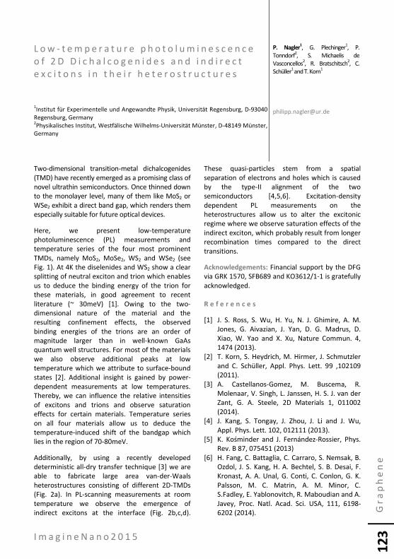
I m a g i n e N a n o 2 0 1 5
Gr
ap
he
ne
123
L o w - t e m p e r a t u r e p h o t o l u m i n e s c e n c e o f 2 D D i c h a l c o g e n i d e s a n d i n d i r e c t e x c i t o n s i n t h e i r h e t e r o s t r u c t u r e s 1Institut für Experimentelle und Angewandte Physik, Universität Regensburg, D-93040 Regensburg, Germany 2Physikalisches Institut, Westfälische Wilhelms-Universität Münster, D-48149 Münster, Germany
Two-dimensional transition-metal dichalcogenides (TMD) have recently emerged as a promising class of novel ultrathin semiconductors. Once thinned down to the monolayer level, many of them like MoS2 or WSe2 exhibit a direct band gap, which renders them especially suitable for future optical devices.
Here, we present low-temperature photoluminescence (PL) measurements and temperature series of the four most prominent TMDs, namely MoS2, MoSe2, WS2 and WSe2 (see Fig. 1). At 4K the diselenides and WS2 show a clear splitting of neutral exciton and trion which enables us to deduce the binding energy of the trion for these materials, in good agreement to recent literature (~ 30meV) [1]. Owing to the two-dimensional nature of the material and the resulting confinement effects, the observed binding energies of the trions are an order of magnitude larger than in well-known GaAs quantum well structures. For most of the materials we also observe additional peaks at low temperature which we attribute to surface-bound states [2]. Additional insight is gained by power-dependent measurements at low temperatures. Thereby, we can influence the relative intensities of excitons and trions and observe saturation effects for certain materials. Temperature series on all four materials allow us to deduce the temperature-induced shift of the bandgap which lies in the region of 70-80meV.
Additionally, by using a recently developed deterministic all-dry transfer technique [3] we are able to fabricate large area van-der-Waals heterostructures consisting of different 2D-TMDs (Fig. 2a). In PL-scanning measurements at room temperature we observe the emergence of indirect excitons at the interface (Fig. 2b,c,d).
These quasi-particles stem from a spatial separation of electrons and holes which is caused by the type-II alignment of the two semiconductors [4,5,6]. Excitation-density dependent PL measurements on the heterostructures allow us to alter the excitonic regime where we observe saturation effects of the indirect exciton, which probably result from longer recombination times compared to the direct transitions.
Acknowledgements: Financial support by the DFG via GRK 1570, SFB689 and KO3612/1-1 is gratefully acknowledged. R e f e r e n c e s
[1] J. S. Ross, S. Wu, H. Yu, N. J. Ghimire, A. M. Jones, G. Aivazian, J. Yan, D. G. Madrus, D. Xiao, W. Yao and X. Xu, Nature Commun. 4, 1474 (2013).
[2] T. Korn, S. Heydrich, M. Hirmer, J. Schmutzler and C. Schüller, Appl. Phys. Lett. 99 ,102109 (2011).
[3] A. Castellanos-Gomez, M. Buscema, R. Molenaar, V. Singh, L. Janssen, H. S. J. van der Zant, G. A. Steele, 2D Materials 1, 011002 (2014).
[4] J. Kang, S. Tongay, J. Zhou, J. Li and J. Wu, Appl. Phys. Lett. 102, 012111 (2013).
[5] K. Kośminder and J. Fernández-Rossier, Phys. Rev. B 87, 075451 (2013)
[6] H. Fang, C. Battaglia, C. Carraro, S. Nemsak, B. Ozdol, J. S. Kang, H. A. Bechtel, S. B. Desai, F. Kronast, A. A. Unal, G. Conti, C. Conlon, G. K. Palsson, M. C. Matrin, A. M. Minor, C. S.Fadley, E. Yablonovitch, R. Maboudian and A. Javey, Proc. Natl. Acad. Sci. USA, 111, 6198-6202 (2014).
P. Nagler1, G. Plechinger1, P.
Tonndorf2, S. Michaelis de Vasconcellos2, R. Bratschitsch2, C. Schüller1 and T. Korn1
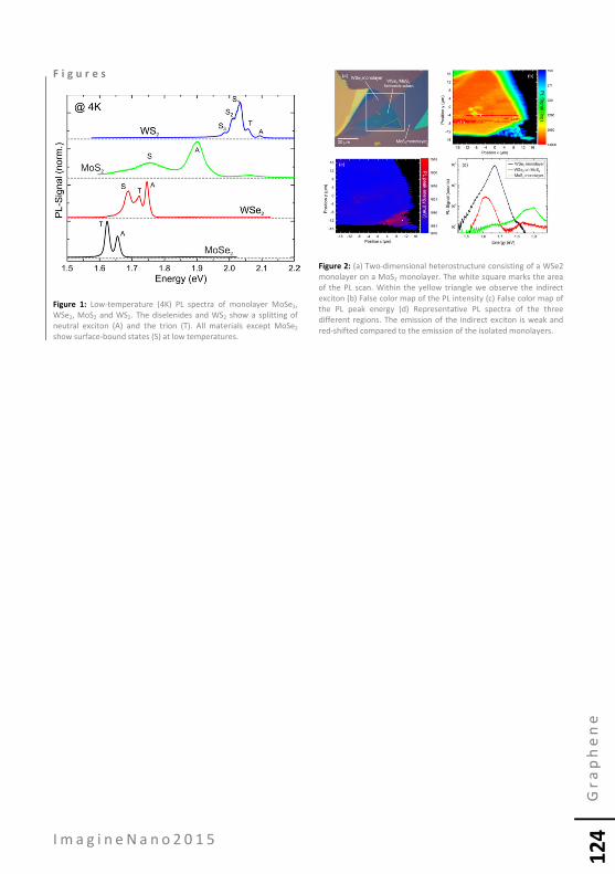
I m a g i n e N a n o 2 0 1 5
Gr
ap
he
ne
124
F i g u r e s
Figure 1: Low-temperature (4K) PL spectra of monolayer MoSe2, WSe2, MoS2 and WS2. The diselenides and WS2 show a splitting of neutral exciton (A) and the trion (T). All materials except MoSe2
show surface-bound states (S) at low temperatures.
Figure 2: (a) Two-dimensional heterostructure consisting of a WSe2 monolayer on a MoS2 monolayer. The white square marks the area of the PL scan. Within the yellow triangle we observe the indirect exciton (b) False color map of the PL intensity (c) False color map of the PL peak energy (d) Representative PL spectra of the three different regions. The emission of the indirect exciton is weak and red-shifted compared to the emission of the isolated monolayers.

I m a g i n e N a n o 2 0 1 5
Gr
ap
he
ne
125
G r a p h e n e b a s e d o p t i c a l m o d u l a t o r s a n d p h o t o d e t e c t o r s f o r c h i p -i n t e g r a t e d c o m m u n i c a t i o n s y s t e m s AMO GmbH Otto-Blumenthal-Strasse 25 52074 Aachen Germany
High frequency opto-electronic devices like photodetectors and electro-optical modulators are the core of modern information and communication systems. Those devices have been recognized from the very beginning as one of the most promising fields of applications for graphene having the potential to significant outperform their counterparts based on Silicon and III/V semiconductors in terms of speed. This expectation has mainly been fuelled by graphene’s tunable, broadband optical interaction, the outstanding charge carrier mobility, and the possibility to integrate graphene on nearly any platform. The on-chip integration of different optical components is the major route for further increasing the bandwidth and reducing cost. While silicon is a perfect material for guiding and routing infrared light, the low light-interaction of silicon requires hetero-integration of other materials for realizing compact modulators and photodetectors. This offers an excellent opportunity for graphene to enter silicon technology by adding missing functionalities. In this talk I will discuss our latest results on grapheme based photodetectors and modulators integrated on silicon waveguides [1,2]. Key parameters will be assessed and compared with competing technologies. R e f e r e n c e s [1] D. Schall, et al. 50 GBit/s photodetectors
based on wafer-scale graphene for integrated silicon photonic communication systems ACS Photonics 1, 781 (2014)
[2] M. Mohsin, D. Schall, M. Otto, A. Noculak, D. Neumaier, and H. Kurz, Graphene based low insertion loss electro-absorption modulator on SOI waveguide Optics Express. 22, 15292 (2014).
F i g u r e s
Daniel Neumaier

I m a g i n e N a n o 2 0 1 5
Gr
ap
he
ne
126
E n v i r o n m e n t a l r e m e d i a t i o n o f o x i d i s e d g r a p h e n e n a n o c a r b o n s : 2 D s h e e t s d e g r a d e f a s t e r t h a n 1 D t u b u l a r - s h a p e d s t r u c t u r e s 1Nanomedicine Lab, Faculty of Medical & Human Sciences & National Graphene Institute, University of Manchester, AV Hill Building, Manchester M13 9PT, United Kingdom 2Nanotube Research Center, National Institute of Advanced Industrial Science and Technology, Tsukuba 305-8565, Japan
Graphene nanocarbons are currently fuelling a revolution in science and technology in areas ranging from aerospace engineering to electronics [1]. Unlike their pristine forms, the oxidised derivatives of those nanostructures are water dispersible that allows their application to areas such as biology and medicine [2]. There is a need for efficient and viable means of degrading these engineered structures that is relevant to their potential biological uses but also for environmental purposes [2, 3]. The aim of the present study was to assess the potential of the widely used sodium hypochlorite, NaClO, (1% by chlorine content) to degrade oxidised graphene nanocarbons within a week. NaClO was found by a risk assessment report completed by the European Union (EEC 793/93) to be safe for the environment with regards to its standard usage which includes domestic sanitation as well as municipal water and waste disinfection. We compared the morphological changes that occur during degradation of graphene oxide to two other oxidised graphene nanocarbons, namely oxidised multiwalled carbon nanotubes and oxidised carbon nanohorns. Degradation was monitored closely using a battery of techniques including UV-Vis, Raman spectroscopy, transmission electron microscopy and atomic force microscopy. The results demonstrate that graphene oxide was degraded into a dominantly amorphous structure lacking the characteristic Raman signature and microscopic (TEM/AFM) morphology. Oxidised carbon nanotubes underwent degradation via a wall exfoliation mechanism, yet maintained a large fraction of the sp2 carbon backbone, while the degradation rate of oxidised carbon nanohorns was observed at a somewhat intermediate rate to that for the other two types of nanostructures.
R e f e r e n c e s [1] Geim, A. K. & Novoselov, K. S., Nat Mater, 6
(2007) 183-91. [2] Kostarelos, K. & Novoselov, K. S., Science,
344 (2014) 261-263. [3] Lalwani, G., Xing, W. & Sitharaman, B., J
Mater Chem B Mater Biol Med, 2 (2014) 6354 6362.
F i g u r e s
Figure 1: Schematic representation of the inferred progressive decay of structural integrity of graphene oxide, oxidised multiwalled carbon nanotubes and oxidised carbon Nanohorns over time when incubated in NaClO 1%.
LDD. Newman1, N. Lozano1, M.
Zhang2, M. Yudasaka M2, C. Bussy1, K. Kostarelos1

I m a g i n e N a n o 2 0 1 5
Gr
ap
he
ne
127
S e a m l e s s s t i t c h i n g o f g r a p h e n e d o m a i n s o n p o l i s h e d c o p p e r ( 1 1 1 ) f o i l
IBS Center for Integrated Nanostructure Physics Institute for Basic Science (IBS), Sungkyunkwan University Suwon, 440-746, Republic of Korea
Graphene grain boundaries (GGBs) are inevitably formed via stitching of graphene flakes, consequently limiting the graphene quality. There have been numerous reports that GGBs are a primary carrier scattering source, thus degrading the related device performance. Therefore, it is always desired to obtain large-area graphene without forming GGBs. Two approaches exit for to synthesizing monocrystalline graphene. One approach is to reduce the number of nucleation seeds. However, large-area growth is terminated by an unknown self-limiting growth factor and requires long growth time. Another approach entails the alignment of graphene domains while leading them to stitch together to form uniform single monocrystalline graphene. Thus, seamless stitching of graphene domains during chemical vapor deposition (CVD) is an ideal concept to realize large-area monocrystalline graphene. Cu(111) substrate maintains hexagonal symmetry with minimum lattice mismatch with graphene and has been tried to grow graphene but no evidence for seamless stitching has been provided. Use of copper substrate is technologically relevant, since monolayer graphene is easily tailored due to the limited carbon solubility in copper, and moreover the surface morphology can be controlled at large area with low cost. In this work, we prove the concept of seamless stitching without forming GGBs by preparing a polished Cu(111) foil for CVD. The seamless stitching was realized by merging hexagonal graphene domains in the same orientation and verified by not only at atomic scale by scanning tunneling microscopy (STM) and transmission electron microscopy (TEM) but also at macro-scale by optical microscopy after UV-treatment[1]. This was markedly distinct from the clear GGBs formed by the similar hexagonal
domains in different orientations, in congruent with our density-functional calculations. This concept was extended to synthesize monocrystalline graphene of 3x6 cm2 size by CVD for an hour by merging multiple hexagonal graphene domains in the same orientation on Cu(111) foil. The mono-crystalinity of the large-area sample was confirmed by new observation method achieved by correlating confocal Raman mapping on overlapped graphene bilayers to polarized optical microscopy (POM) on spin-casted nematic liquid crystal (NLC) layer, combined with transport measurements at the stitched region. R e f e r e n c e s [1] Van Luan Nguyen et al, Advanced Materials,
(2014), just accepted F i g u r e s
Van Luan Nguyen, Young Hee Lee

I m a g i n e N a n o 2 0 1 5
Gr
ap
he
ne
128
D e f e c t m o d u l a t e d p h o t o r e s p o n s e a n d t h e r m a l c o n d u c t i v i t y i n g r a p h e n e 1 Department of Physics, Southeast University, Nanjing 211189, China 2 School of mechanical engineering, Southeast University, Nanjing 211189, China 3 Graphene Research and Characterization Center, Taizhou Sunano New Energy Co., Ltd. Taizhou, 225300, China There is a great need for controlling the properties of two dimensional (2D) materials to fulfill the requirements of various applications.[1-4] Here, we present our results on the modulation of the properties of graphene by controllably introducing different types of defects. Firstly, the graphene-based photodetector with tunable p-p+-p junctions has been successfully fabricated using a simple laser modification method. Distinct photoresponse was observed at the graphene (G)- laser-modified graphene (LMG) junction through scanning photocurrent measurements, and Raman spectra reveal that defects are created at the LMG region. Detailed investigation suggests that the photo-thermoelectric effect, instead of the photovoltaic effect, dominates the photocurrent generation at the G-LMG junctions. Secondly, we adopted molecular dynamics simulations and non-contact optothermal Raman measurements to identify the correlation between the lattice defects and thermal conduction transport in graphene. We find that the thermal conductivity of graphene can be significantly reduced even at extremely low defect concentration (~83% reduction for ~1‰ defects), where defects act as localized scatters and greatly reduce the conductivity. Our findings provide fundamental insights into the physics of thermal transport in graphene, and two-dimensional materials in general, which could help on the future design of functional applications such as optothermal and electrothermal devices. R e f e r e n c e s [1] Ni ZH, Ponomarenko LA, Nair RR, Yang R,
Anissimova S, Grigorieva IV, Schedin F, Shen ZX, Hill EH, Novoselov KS, Geim AK On
resonant scatterers as a factor limiting carrier mobility in grapheme, Nano Letters 10, 3868-3872 (2010).
[2] Zhan D, Yan JX, Lai LF, Ni ZH, Liu L, Shen ZX Engineering the electronic structure of grapheme, Advanced Materials 24, 4055-4069 (2012).
[3] Liu YL, Nan HY, Wu X, Pan W, Wang WH, Bai J, Zhao WW, Sun LT, Wang XR, Ni ZH* Layer-by-Layer Thinning of MoS2 by Plasma. ACS Nano 7, 4202, (2013).
[4] Nan HY, Wang ZL, Wang WH, Liang Z, Lu Y, Chen Q, He DW, Tan PH, Miao F, Wang XR, Wang JL*, Ni ZH* Strong Photoluminescence Enhancement of MoS2 through Defect Engineering and Oxygen Bonding ACS Nano 8, 5738 (2014).
F i g u r e s
Figure 1: Photocurrent image of graphene before (a) and after laser modification at different positions: P1 (b), P2 (c), P3 (d), respectively. (e) Photoswitching characteristic at the bottom spot near LMG (P3) (P3(B)). (f) Photocurrents as function of the laser power detected at regions near P3 and graphene-metal contacts as marked in (d).
Zhenhua Ni1, Wenhui Wang1,
Weiwei Zhao2, Zheng Liang3
I m a g i n e N a n o 2 0 1 5
Gr
ap
he
ne
20
15
129
H y b r i d g r a p h e n e – q u a n t u m d o t p h o t o t r a n s i s t o r s f o r I R - i m a g i n g a p p l i c a t i o n s 1 ICFO – The Institute of Photonic Sciences, Av. Carl Friedrich Gauss 3, 08860 Castelldefels (Barcelona), Spain
Graphene is an appealing material for optoelectronics and photodetection applications. It has various extraordinary properties, including ultrahigh mobility at room temperature, which enables fast response times. Colloidal quantum dots exhibit unique optical properties of spectral tunability and high absorption coefficients. We combine the favourable electronic properties of graphene with the optical characteristics of colloidal quantum dots to realize a novel hybrid graphene-quantum dot photodetector for visible and short-wave infrared frequencies. [1] The unique electronic properties of graphene offer a gate-tunable carrier density and polarity that enabl us to tune the sensitivity and operating speed of the detector. Here, we exploit this to maximize the photoconductive gain or to fully reduce it to zero, which is useful for pixelated imaging applications, while the implementation of nanoscale local gates enables a locally tunable photoresponse. We also demonstrate our novel approach to fully suppress dark currents in graphene-based photodetectors and increase operation speed of our devices. At
the current state our single- and multipixel photodetectors can operate at 30, 60 and up to 90 frames-per-second. The resulting technology is extremely promising for visible and, more importantly, short-wave infrared (SWIR) imaging applications. Sensing and imaging in SWIR range lies at the heart of safety and security applications in civil and military surveillance, night vision applications, automotive vision systems for driver safety, food and pharmaceutical inspection and environmental monitoring. Operation of a prototype device sensitive to visible and IR light in the auditorium will be demonstrated during the talk. R e f e r e n c e s [1] Gerasimos Konstantatos, Michela Badioli,
Louis Gaudreau, Johann Osmond, Maria Bernechea, F. Pelayo Garcia de Arquer, Fabio Gatti and Frank H. L. Koppens, Nature Nanotechnology, 7 (2012) 363–368.
Ivan Nikitskiy1, A.M. Goossens1, G.
Navickaite1, J. J. Piqueras1, G. Konstantatos1 and F.H. L. Koppens1

I m a g i n e N a n o 2 0 1 5
Gr
ap
he
ne
20
15
130
G r a p h e n e n a n o p o r e s f o r b i o s e n s i n g a n d t h e r m o e l e c t r i c a p p l i c a t i o n s : F i r s t -p r i n c i p l e s q u a n t u m t r a n s p o r t s i m u l a t i o n Department of Physics & Astronomy, University of Delaware Newark, DE 19716, USA https://wiki.physics.udel.edu/qttg
Mechanical stability of graphene and advances in nanofabrication have recently made possible drilling of tiny holes (or arrays of such holes) of nanoscale diameter within graphene sheets. The experimental demonstration of DNA translocation through graphene nanopores has opened new avenues for third-generation DNA sequencing, where unlike traditionally considered biological or solid-state nanopores, one-atom-thickness of graphene means that only one nucleobase is present within the nanopore. However, the poor signal-to-noise ratio achieved in sensing of nucleobases within the nanopore via vertical ionic current calls for new ideas to exploit electronic transport in the plane of graphene. Using nonequilibrium Green function formalism combined with density functional theory (NEGF+DFT) simulations, we have predicted [1,2] that using edge currents in zigzag or chiral graphene nanoribbons (GNR) could significantly improve signal-to-noise ratio, thereby enabling ultrafast DNA sequencing.
An array of graphene nanopores can also be used to significantly impede the lattice thermal conduction through GNRs, decorated with heavy adatoms to locally enhance spin-orbit coupling and convert GNR into a two-dimensional topological insulator. The nanopores do not affect electronic current carried by helical edge states, which generate a highly optimized power factor per helical conducting channel due to narrow boxcar-function-shaped electronic transmission (surpassing even the so-called Mahan-Sofo limit obtained for delta function-shaped electronic transmission). In Ref. [3], we have predicted that thermoelectric figure of merit of GNR + heavy adatoms + nanopores system would reach its maximum ZT~3 at low temperatures, T~40 K,
which paves a way to design high-ZT materials by exploiting the nontrivial topology of electronic states through nanostructuring.
In this talk, I will overview these two classes of graphene nanopore devices, illustrated in Fig. 1, as well as challenges for NEGF+DFT simulations applied to their design and modeling.
R e f e r e n c e s
[1] K. K. Saha, M. Drndić, and B. K. Nikolić, Nano Lett. 12, 50 (2012).
[2] P.-H. Chang, H. Liu, and B. K. Nikolić, J. Comput. Electron. 13, 847 (2014).
[3] P.-H. Chang, M. S. Bahramy, N. Nagaosa, and B. K. Nikolić, Nano Lett. 14, 3779 (2014).
F i g u r e s
Figure 1: Schematic view of a single nanopore within GNR with zigzag or chiral edges for ultrafast DNA sequencing (top panel) [1,2]; or an array of nanopores within GNR (with arbitrary edges) and heavy adatoms for high-ZT thermoelectric applications by exploiting the nontrivial topology of electronic states (bottom panel) [3].
Branislav K. Nikolić
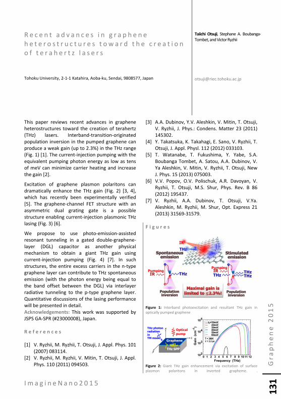
I m a g i n e N a n o 2 0 1 5
Gr
ap
he
ne
20
15
131
R e c e n t a d v a n c e s i n g r a p h e n e h e t e r o s t r u c t u r e s t o w a r d t h e c r e a t i o n o f t e r a h e r t z l a s e r s Tohoku University, 2-1-1 Katahira, Aoba-ku, Sendai, 9808577, Japan
This paper reviews recent advances in graphene heterostructures toward the creation of terahertz (THz) lasers. Interband-transition-originated population inversion in the pumped graphene can produce a weak gain (up to 2.3%) in the THz range (Fig. 1) [1]. The current-injection pumping with the equivalent pumping photon energy as low as tens of meV can minimize carrier heating and increase the gain [2].
Excitation of graphene plasmon polaritons can dramatically enhance the THz gain (Fig. 2) [3, 4], which has recently been experimentally verified [5]. The graphene-channel FET structure with an asymmetric dual grating gate is a possible structure enabling current-injection plasmonic THz lasing (Fig. 3) [6].
We propose to use photo-emission-assisted resonant tunneling in a gated double-graphene-layer (DGL) capacitor as another physical mechanism to obtain a giant THz gain using current-injection pumping (Fig. 4) [7]. In such structures, the entire excess carriers in the n-type graphene layer can contribute to THz spontaneous emission (with the photon energy being equal to the band offset between the DGL) via interlayer radiative tunneling to the p-type graphene layer. Quantitative discussions of the lasing performance will be presented in detail. Acknowledgements: This work was supported by JSPS GA-SPR (#23000008), Japan. R e f e r e n c e s [1] V. Ryzhii, M. Ryzhii, T. Otsuji, J. Appl. Phys. 101
(2007) 083114. [2] V. Ryzhii, M. Ryzhii, V. Mitin, T. Otsuji, J. Appl.
Phys. 110 (2011) 094503.
[3] A.A. Dubinov, Y.V. Aleshkin, V. Mitin, T. Otsuji, V. Ryzhii, J. Phys.: Condens. Matter 23 (2011) 145302.
[4] Y. Takatsuka, K. Takahagi, E. Sano, V. Ryzhii, T. Otsuji, J. Appl. Physl. 112 (2012) 033103.
[5] T. Watanabe, T. Fukushima, Y. Yabe, S.A. Boubanga Tombet, A. Satou, A.A. Dubinov, V. Ya Aleshkin, V. Mitin, V. Ryzhii, T. Otsuji, New J. Phys. 15 (2013) 075003.
[6] V.V. Popov, O.V. Polischuk, A.R. Davoyan, V. Ryzhii, T. Otsuji, M.S. Shur, Phys. Rev. B 86 (2012) 195437.
[7] V. Ryzhii, A.A. Dubinov, T. Otsuji, V.Ya. Aleshkin, M. Ryzhii, M. Shur, Opt. Express 21 (2013) 31569-31579.
F i g u r e s
Figure 1: Interband photoexcitation and resultant THz gain in optically pumped graphene
Figure 2: Giant THz gain enhancement via excitation of surface plasmon polaritons in inverted grapheme. .
Taiichi Otsuji, Stephane A. Boubanga-Tombet, and Victor Ryzhii

I m a g i n e N a n o 2 0 1 5
Gr
ap
he
ne
20
15
132
T r a n s p o r t S t u d i e s i n B l a c k P h o s p h o r u s F i e l d E f f e c t T r a n s i s t o r s Centre for Advanced 2D Materials and Graphene Research Centre National University of Singapore Singapore 117546 Department of Physics National University of Singapore Singapore 117542
Ultrathin black phosphorus (BP), or phosphorene is the second known elementary two-dimensional material that can be exfoliated from a bulk van der Waals crystal. Unlike graphene it is a semiconductor with a sizeable band gap that allows both high carrier mobility and large on/off ratios. Its excellent electronic properties make it attractive for applications in transistor, logic, and optoelectronic devices. However, it is also the first widely investigated two dimensional electronic material to undergo degradation upon exposure to ambient air. Therefore a passivation method is required to study the intrinsic material properties,
understand how oxidation affects the physical transport properties and to enable future application of phosphorene. I will show that atomically thin graphene and hexagonal boron nitride crystals can be used for passivation of ultrathin black phosphorus. I will also discuss experiments where we characterize few-layer black phosphorus field effect transistors on hexagonal boron nitride (BN) and compare with results obtained with BP fully encapsulated with BN.
Barbaros Özyilmaz

I m a g i n e N a n o 2 0 1 5
Gr
ap
he
ne
20
15
133
O p t i m i z e d g r a p h e n e g r o w t h o n G e ( 1 0 0 ) / S i ( 1 0 0 ) s u b s t r a t e s 1 Institute of Electronic Materials Technology, Wolczynska 133, 01-919 Warsaw, Poland 2 IHP, Im Technologiepark 25, 15236 Frankfurt (Oder), Germany 3 Institute of Optoelectronics, Military University of Technology, Gen. S. Kaliskiego 2, 00-908 Warsaw, Poland
In order to widen the range of possible graphene applications, for example in high frequency electronics, it is desirable to grow graphene films directly on arbitrary insulator or semiconductor surfaces instead of on a most commonly used copper substrate. Ideally such insulating or semiconducting layers are deposited on Si wafers used commonly in integrated circuit (IC) manufacturing. Growing graphene directly on Si wafer surface is extremely challenging due to the tendency to form carbides. This tendency is much weaker when Ge is used as the substrate instead of Si [1], which has been exploited to grow high quality graphene on Ge(110)/Si(110) wafers [2]. Here, we present for the first time a CVD growth of graphene on monocrystalline Ge(100) “virtual substrates” deposited on Si(100) wafers which is the preferred wafer orientation in the mainstream Si IC fabrication. This approach benefits from the cost advantage and manufacturing compatibility of Si(100) wafers and avoids the metal contamination problems and complexity associated with graphene transfer from Cu. A clean, high quality graphene grown on Ge(100)/Si(100) wafers can be subsequently either transferred using wafer bonding approaches or used directly for fabrication of e.g. graphene THz devices [3] thus opening the way for this new material to the integration with Si microelectronics. In the present work graphene films were synthesized in a 6-inch Black Magic system by the CVD method. As a substrate we used both 1 µm and 3 µm thick (100) oriented Ge deposited on Si(100). To ensure optimal temperature conditions,
thus preventing Si diffusion through a Ge layer and Ge melting the temperature was chosen in the range between 900ºC and 930ºC with a slow ramp. During the process of graphene deposition the pressure of 700 mbar was sustained. Methane gas was used as a carbon precursor in the mixture of Ar and H2. We optimized the ratio of Ar/H2/CH4 gases, growth time and temperature so that a continuous film was created. Furthermore, we developed the process of transferring graphene from Ge/Si wafers onto dielectric substrates aimed at showing clear and non-contaminated graphene films. The assessment of the properties of graphene grown on Ge/Si substrates was performed using Raman spectroscopy, which confirmed the formation of graphitic structures and their quality, and SEM imaging, which showed the morphology of the graphene/Ge/Si interaction. For the purpose of electrical measurements by the Hall method and the contamination detection by performing the ToF-SIMS analysis, we developed a protocol of graphene transfer onto a dielectric substrate. R e f e r e n c e s [1] G. Lippert, et al Carbon 75, 104 (2014). [2] Lee et al, Science Vol. 344 no. 6181 (2014) pp.
286-289. [3] V. Di Lecce, R. Grassi, A. Gnudi, E. Gnani, S.
Reggiani, G. Baccarani, Trans. Electron Dev., 60 (2013) 4263.
.
I. Pasternak1, M. Lukosius2, Y.
Yamamoto2, A. Krajewska1,3, G. Lupina2
and W. Strupinski1
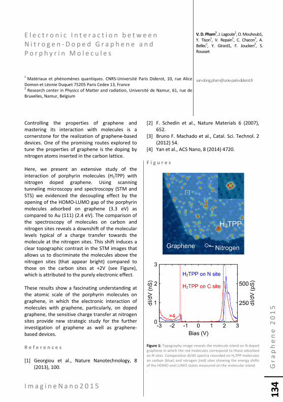
I m a g i n e N a n o 2 0 1 5
Gr
ap
he
ne
20
15
134
E l e c t r o n i c I n t e r a c t i o n b e t w e e n N i t r o g e n - D o p e d G r a p h e n e a n d P o r p h y r i n M o l e c u l e s 1 Matériaux et phénomènes quantiques. CNRS-Université Paris Diderot, 10, rue Alice Domon et Léonie Duquet 75205 Paris Cedex 13, France 2 Research center in Physics of Matter and radiation, Université de Namur, 61, rue de Bruxelles, Namur, Belgium
Controlling the properties of graphene and mastering its interaction with molecules is a cornerstone for the realization of graphene-based devices. One of the promising routes explored to tune the properties of graphene is the doping by nitrogen atoms inserted in the carbon lattice. Here, we present an extensive study of the interaction of porphyrin molecules (H2TPP) with nitrogen doped graphene. Using scanning tunneling microscopy and spectroscopy (STM and STS) we evidenced the decoupling effect by the opening of the HOMO-LUMO gap of the porphyrin molecules adsorbed on graphene (3.3 eV) as compared to Au (111) (2.4 eV). The comparison of the spectroscopy of molecules on carbon and nitrogen sites reveals a downshift of the molecular levels typical of a charge transfer towards the molecule at the nitrogen sites. This shift induces a clear topographic contrast in the STM images that allows us to discriminate the molecules above the nitrogen sites (that appear bright) compared to those on the carbon sites at +2V (see Figure), which is attributed to the purely electronic effect. These results show a fascinating understanding at the atomic scale of the porphyrin molecules on graphene, in which the electronic interaction of molecules with graphene, particularly, on doped graphene, the sensitive charge transfer at nitrogen sites provide new strategic study for the further investigation of graphene as well as graphene-based devices. R e f e r e n c e s [1] Georgiou et al., Nature Nanotechnology, 8
(2013), 100.
[2] F. Schedin et al., Nature Materials 6 (2007), 652.
[3] Bruno F. Machado et al., Catal. Sci. Technol. 2 (2012) 54.
[4] Yan et al., ACS Nano, 8 (2014) 4720. F i g u r e s
Figure 1: Topography image reveals the molecule island on N doped graphene in which the red molecules correspond to those adsorbed on N sites. Comparative dI/dV spectra recorded on H2TPP molecules on carbon (blue) and nitrogen (red) sites showing the energy shifts of the HOMO and LUMO states measured on the molecular island. .
V. D. Pham1, J. Lagoute1, O. Mouhoub1,
Y. Tison1, V. Repain1, C. Chacon1, A. Bellec1, Y. Girard1, F. Joucken2, S. Rousset

I m a g i n e N a n o 2 0 1 5
Gr
ap
he
ne
20
15
135
I n f l u e n c e o f s u b s t r a t e t e m p e r a t u r e a n d S i C b u f f e r l a y e r o n t h e q u a l i t y o f g r a p h e n e f o r m a t i o n d i r e c t l y o n S i ( 1 1 1 ) 1
Research Center in Physics of Matter and Radiation (PMR), University of Namur (FUNDP), 61 Rue de Bruxelles, 5000 Namur, Belgium 2 Nanoscopic physics (NAPS), Institute of Condensed Matter and Nanosciences (IMCN), Université catholique de Louvain (UCL), 2 chemin du Cyclotron, Louvain-la-Neuve, Belgium 3 Electrical Engineering (ELEN), Institute of Information and Communication Technologies, Electronicsand Applied Mathematics (ICTEAM), Université catholique de Louvain (UCL), 3 place du Levant, Louvain-la-Neuve, Belgium
Evidence for the epitaxial growth of graphene films directly on Si(111) 7×7 surface reconstruction was demonstrated (Fig. 1), however the production of low surface roughness and large area graphene on Si wafer is still a challenge in the context of direct deposition of carbon atoms using an electron beam evaporator [1, 2]. Therefore, in order to optimize this film for approaching industrial applications, in this paper we continue investigating the structural and electronic properties of our material at various substrate temperatures using covered SiC buffer layers with different thicknesses under appropriate preparation by Auger electron spectroscopy, X-ray photoemission spectroscopy, Raman spectroscopy, scanning electron microscopy and scanning tunneling microscopy. Recorded experimental results confirm this significant influence on the quality of graphene formation. This method might be very promising for graphene-based electronics and its integration into the silicon technology. R e f e r e n c e s [1] Pham Thanh Trung, Frederic Joucken, Jessica
Campos-Delgado, Jean-Pierre Raskin, Benoit Hackens, and Robert Sporken, Appl. Phys. Lett. 102, 013118 (2013).
[2] Pham Thanh Trung, Jessica Campos-Delgado, Frédéric Joucken, Jean-François Colomer, Benoıt Hackens, Jean-Pierre Raskin, Cristiane N. Santos, and Sporken Robert, J. Appl.Phys. 115, 223704 (2014).
F i g u r e s
Figure 1: An atomic resolution STM image of 30×30Å2 (VSample = -0.12V, IT = 10nA) from graphene films on Si(111) 7x7 surface reconstruction showing the AB (Bernal) stacking order of a typical graphene lattice [2].
Trung T. Pham1, Cristiane N. Santos2,
Frédéric Joucken1, Benoît Hackens2, Jean-Pierre Raskin3 and Robert Sporken1

I m a g i n e N a n o 2 0 1 5
Gr
ap
he
ne
20
15
136
E x c i t o n i c t r a n s i t i o n s i n 2 D t r a n s i t i o n m e t a l d i c h a l c o g e n i d e s ( M o S 2 , W S 2 a n d W S e 2 ) 1 Departamento de Fisica Universidade Federal de Minas Gerais (UFMG), Brazil 2 Department of Physics, Applied Physics and Astronomy, RPI, Troy, NY, USA 3 Department of Physics and Center for 2-D and Layered Materials, The Pennsylvania State University, University Park, USA
Resonance Raman spectroscopy (RRS) is a very useful tool to provide information about excitons and their couplings with phonons. We will present in this work a RRS study of different samples of 2D transition metal dichalcogenides (MoS2, WS2 and WSe2) with one, two and three layers (1L, 2L, 3L) and bulk samples, using more than 30 different laser excitation lines covering the visible range. We have observed that all Raman features are enhanced by resonanceswith excitonic transitions. From the laser energy dependence of the Raman excitation profile (REP) we obtained the energies of the excitonic states and their dependence with
the number of atomic layers. The first and second-order Raman features exhibit different resonance behaviors, in agreement with the double resonance mechanism for the second-order Raman features. In the case of MoS2, we observed that the electronphonon coupling is symmetry dependent, and we provide evidence of the C exciton recently predicted theoretically. The RRS results WSe2 show that the Raman modes are enhanced by the excited excitonic states (A’ and B’) and we will present the dependence of the excited states energies on the number of layers.
Marcos A. Pimenta1, Elena del Corro1,
Bruno R. Carvalho1, Leandro M. Malard1, Juliana M. Alves1, Humberto Terrones2, Ana L. Elias3, Mauricio Terrones3 and Cristiano Fantini1

I m a g i n e N a n o 2 0 1 5
Gr
ap
he
ne
20
15
137
U l t r a f a s t b r o a d b a n d s t u d y o f p h o t o c a r r i e r d y n a m i c s i n M o S 2 s i n g l e l a y e r 1 Politecnico di Milano, P.zza Leonardo da Vinci 32, 20133, Milano, Italy 2 CNR-Istituto Nanoscienze, 41125 Modena, Italy 3 CNR-Istituto di Struttura della Materia, Montelibretti, Italy 4 Cambridge Graphene Centre, Cambridge, CB3 OFA, UK
We present a time-resolved study of charge carrier dynamics in single-layer MoS2 (1L-MoS2) by ultrafast transient absorption spectroscopy. Using tunable pump pulses and broadband probing, we monitor the relaxation dynamics of the photo-excited states with unprecedented spectral coverage (the entire visible range). The sample is a 10 x 30 µm2 1L-MoS2 prepared by micromechanical exfoliation and transferred onto a transparent fused silica substrate [1]. The transient absorption spectrum has three prominent features, each consisting of a bleaching at the energies of the excitonic transitions A, B C (at 1.9, 2.1 and 2.9 eV) and a red-shifted photoinduced absorption, Fig. 1. These features do not depend on the excitation energy, which is tuned to be resonant and non-resonant with the excitonic transitions. Pauli blocking cannot explain, alone, the simultaneous bleaching of the three excitonic transitions and the corresponding photoinduced absorption. Instead, we believe that a transient band gap renormalization caused by the presence of photo-excited carriers should be also considered. A static strong renormalization of both electronic band gap and exciton binding energy was previously reported in MoSe2 due to the interaction with the substrate [2]. Here we compare our data with simulations combining non-equilibrium Green's functions with ab-initio methods [3,4]. The comparison of experimental data with simulations allows us to shed light on the delicate interplay among Pauli blocking, band gap renormalization and electron-phonon relaxation, which are the key phenomena governing the carrier dynamics after photo-excitation.
R e f e r e n c e s [1] Bonaccorso et al.Materials Today, 15 (2012)
564-589.
[2] M. M. Ugeda et al., Nat. Mat., 13 (2014) 1091-1095.
[3] A. Marini, J. Phys.: Conf. Ser. 427 (2013) 012003; D. Sangalli and A. Marini, arXiv:1409.1706 (2014).
[4] A. Marini, C. Hogan, M Grüning, and D. Varsano, Comp. Phys. Comm., 180 (2009) 1392.
F i g u r e s
Figure 1: Transient Absorption of 1L-MoS2. 100 fs-pulse excitation in the visible range determines simultaneous bleaching of the A, B, C excitons, with the absorption surviving up to hundreds ps. a)
Transient absorption map with λpump= 400nm; b) Transient absorption spectrum at fixed delays; c) Relaxation dynamics of C-
exciton bleaching with λpump = 400, 600 and 650 nm.
E.A.A. Pogna1, S. Dal Conte1, M.
Marsili2, D. Prezzi2, D. Sangalli3, C.Manzoni1, A. Marini3, D. De Fazio4, M. Bruna4, I. Goykhman4, A. C. Ferrari4, G. Cerullo1
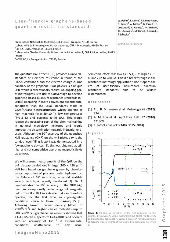
I m a g i n e N a n o 2 0 1 5
Gr
ap
he
ne
20
15
138
U s e r - f r i e n d l y g r a p h e n e - b a s e d q u a n t u m r e s i s t a n c e s t a n d a r d s 1 Laboratoire National de Métrologie et d’Essais, Trappes, 78190, France 2Laboratoire de Photonique et Nanostructures, CNRS, Marcoussis, 91460, France 3CRHEA, CNRS, Valbonne, 06560, France 4Laboratoire Charles Coulomb, Université de Montpellier 2, CNRS, Montpellier, 34095, France 5NOVASiC, Le Bourget du Lac, 73370, France
The quantum Hall effect (QHE) provides a universal standard of electrical resistance in terms of the Planck constant h and the electron charge e. One hallmark of the graphene Dirac physics is a unique QHE which is exceptionally robust. An ongoing goal of metrologists is to use this advantage to develop graphene-based quantum resistance standards (G-QHRS) operating in more convenient experimental conditions than the usual standards made of GaAs/AlGaAs heterostructures which operate at high magnetic fields (B~10 T), low temperatures (T~1.3 K) and currents (I~40 μA). This would reduce the operating cost of the ohm maintaining in national metrology institutes and would improve the dissemination towards industrial end-users. Although the 10-9 accuracy of the quantized Hall resistance (QHR) on the ν=2 plateau (ν is the Landau level filling factor) was demonstrated in a few graphene devices [1], this was obtained at still high and not competitive operating magnetic fields up to now. We will present measurements of the QHR on the ν=2 plateau carried out in large (100 × 420 μm2) Hall bars based on graphene grown by chemical vapor deposition of propane under hydrogen on the Si-face of SiC substrates, a hybrid scalable growth technique recently developed [2]. Fig. 1 demonstrates the 10-9 accuracy of the QHR (RH) over an exceptionally wide range of magnetic fields from B = 10 T in a device that can therefore operate, for the first time, in cryomagnetic conditions similar to those of GaAs-QHRS [3]. Achieving lower carrier density (down to 2x1011cm-2) and higher carrier mobilities (up to 9000 cm2V-1s-1) graphene, we recently showed that a G-QHRS can outperform GaAs-QHRS and operate with an accuracy of 1×10⁻⁹ in experimental conditions unattainable to any usual
semiconductors: B as low as 3.5 T, T as high as 5.1 K, and I up to 280 μA. This is a breakthrough in the resistance metrology application since it opens the era of user-friendly helium-free quantum resistance standards able to be widely disseminated. R e f e r e n c e s
[1] T. J. B. M Janssen et al, Metrologia 49 (2012), 294.
[2] A. Michon et al., Appl.Phys. Lett. 97 (2010), 171909.
[3] F. Lafont et al. arXiv:1407.3615 (2014). F i g u r e s
Figure 1: (a) Relative deviation of the Hall resistance to the quantized value ΔRH/RH versus magnetic field B. b) Hall resistance RH
and longitudinal resistance Rxx versus B (in green for GaAs sample). c) Accurate measurements of the longitudinal resistance Rxx versus
B.
W. Poirier1, F. Lafont1, R. Ribeiro-Palau1,
D. Kazazis2, A. Michon3, B. Jouault4, O. Couturaud4, C. Consejo4, M. Zielinski5, Th. Chassagne5, M. Portail3, B. Jouault4, F. Schopfer1

I m a g i n e N a n o 2 0 1 5
Gr
ap
he
ne
20
15
139
E l e c t r o n i c t r a n s p o r t , n a n o s t r u c t u r i n g a n d d i s o r d e r i n g r a p h e n e Center for Nanostructured Graphene (CNG), Department of Micro- and Nanotechnology (DTU Nanotech), Technical University of Denmark, Denmark
Nanoscale patterning has been suggested as a possible route towards achieving the elusive electronic band-gap required to incorporate graphene, with its many superlative properties, into conventional semiconductor devices. Of particular interest are so-called graphene antidot
lattices (GALs), consisting of sheets of graphene with periodic perforations, which theory predicts should display sizable band-gaps [1]. In this talk I demonstrate that the geometric disorders inherent in fabrication techniques severely hamper the performance of many GAL-based devices. Furthermore, control over antidot edge geometry may allow the detrimental effects of such disorders to be minimized [2]. I will also discuss techniques we have developed to characterize individual defects and nanostructures using multiple point-probes or STM tips. Computational methods developed to extend this type of analysis from simple defects to larger nanostructures such as perforations or gas-filled blisters will be demonstrated [3]. Finally, I will discuss two alternative routes towards achieving desirable electronic properties in graphene, namely bilayer systems with single layer nanostructuring [4] and graphene with selective sublattice doping [5]. R e f e r e n c e s [1] Pederden, T. G. et al, Phys. Rev. B, 77 (2008)
245431. [2] Power, S. R. and Jauho, A.-P., Phys. Rev. B, 90
(2014), 115408. [3] Settnes, M. et al, preprint arXiv:1501.06036
(2015).
[4] Gregersen, S. S. et al, preprint arXiv:1410.5196 (2015)
[5] Aktor et al, in preparation (2015) F i g u r e s
Figure 1: (Top) Schematic of graphene patterned with circular antidots arranged in a triangular superlattice, showing the unit cell of the 7,3 antidot lattice system. (Bottom) Transmission through finite-width antidot barriers for the pristine case, and with edge roughness disorder in the form of weak random potentials on the antidot edge sites (shown for a single instance and for configurationally averaged disorder)
Stephen R. Power, Mikkel Settnes, Søren Schou Gregersen, Thomas Aktor, Antti-Pekka Jauho
spow @ nanotech.dtu.dk

I m a g i n e N a n o 2 0 1 5
Gr
ap
he
ne
20
15
140
A t o m - b y - a t o m d e f e c t e n g i n e e r i n g a n d c h a r a c t e r i s a t i o n i n g r a p h e n e a n d o t h e r 2 - d i m e n s i o n a l m a t e r i a l s u s i n g s c a n n i n g t r a n s m i s s i o n e l e c t r o n m i c r o s c o p y 1 SuperSTEM Laboratory, SciTech Daresbury Campus, Keckwick Lane, Daresbury WA4 4AD, U.K. 2Institute for Materials Research, SCAPE, University of Leeds, Leeds LS2 9JT, U.K. 3Faculty of Physics, University of Vienna, Boltzmanngasse 5, A-1090 Vienna, Austria 4Department of Physics and Energy, University of Limerick, Limerick, Ireland
Modern aberration-corrected scanning transmission electron microscopes (STEMs) have been optimised to provide improved data collection ability and greater flexibility even at low acceleration voltages, to the great benefit of the field of graphene and two-dimensional materials. By reducing the acceleration voltage to overcome knock-on damage limitations, many of these structures can be imaged directly at atomic resolution, revealing for instance the successful low energy ion implantation of single N or B dopants in graphene with retention rates consistent with theoretical predictions, a technique commonly used by the modern semiconductor industry and which has the potential to revolutionize graphene technology [1]. Furthermore, the sensitivity of complementary analytical techniques such as electron energy loss spectroscopy (EELS) is such that it also possible to study precisely how these atoms bonded to one another and how minute structural differences affect their electronic configuration [2,3]. In particular, EELS fine structure differences can distinguish unambiguously between tri- and tetravalent bonding configurations of single Si contaminants in graphene [2], while a clear signature in the near-edge fine structure of the B and N EELS K edges but also that of neighboring C atoms and their EELS K edges (Figure 1) provide evidence of electronic structure modifications due to presence of the dopants. Ab initio calculations are used simulate experimental spectra and to rationalize the experimental observations, thus providing further insight into the nature of bonding around the foreign species [3]. Finally, these otherwise 'gentle' STEM observation conditions can also be precisely tailored to engineer and modify defects in 2-dimensional materials: the electron beam can thus drive the
diffusion of substitutional Si dopants through graphene (Figure 2), one atomic jump at a time [4].
R e f e r e n c e s
[1] U. Bangert, W. Pierce, D.M. Kepaptsoglou et al., Nano Lett. 13 (2013), p. 4902.
[2] Q.M. Ramasse, C.R. Seabourne, D.M. Kepaptsoglou et al., Nano Lett. 12 (2012), p. 3936.
[3] D.M. Kepaptsoglou, C.R. Seabourne, R. Nicholls et al., Submitted (2015).
[4] T. Susi, J. Kotakoski, D. Kepaptsoglou et al., Phys. Rev. Lett. 113 (2014), 115501.
F i g u r e s
Figure 1: Atomically resolved EELS map (b), showing a single N dopant in the graphene lattice (a-b). C K edge spectra (d) from neighboring C atoms, show changes in their near-edge fine structure.
Figure 2: A single Si substitutional impurity in graphene can undergo a bond inversion with its neighbouring C atoms under a 60kV electron beam.
Quentin M. Ramasse1, Demie M.
Kepaptsoglou1, Che R. Seabourne2, Trevor Hardcastle2, Andrew Scott2, Toma Susi3, Jani Kotakoski3, Jannik C. Meyer3, Recep Zan4 and Ursel Bangert4
I m a g i n e N a n o 2 0 1 5
Gr
ap
he
ne
20
15
141
I n d u s t r i a l i z a t i o n a n d S t a n d a r d i z a t i o n o f G r a p h e n e M a t e r i a l s i n C h i n a Shenyang National Laboratory for Materials Science Institute of Metal Research, Chinese Academy of Sciences Shenyang 110016, P.R. China
Graphene materials have attracted increasing interest from academic and industrial societies because of their excellent properties and a wide range of promising applications. In particular, the research and industrialization of graphene materials in China has been developing very rapidly in the past several years. Many graphene-related companies have been established for large-
scale production of grapheme materials aimed at industrial applications, which makes an urgent call for the standardization of graphene materials. This talk will briefly summarize the progress of industrialization and standardization of graphene materials in China, and challenges and prospects in these fields will be discussed.
Wencai Ren

I m a g i n e N a n o 2 0 1 5
Gr
ap
he
ne
20
15
142
S p e c t r a l S e n s i t i v i t y o f p n - j u n c t i o n P h o t o d e t e c t o r s b a s e d o n 2 D m a t e r i a l s 1 University of Siegen, Hölderlinstrasse 3, 57076 Siegen, Germany 2 School of Chemistry, Trinity College Dublin, Dublin 2, Ireland
Broad spectral range detection is interesting for several technological applications such as imaging, sensing, communication and spectroscopy. Two-dimensional (2D) materials are very promising for such applications. Graphene is a suitable material for broadband detection due to its absorbance covering the entire spectrum from ultraviolet to terahertz, which is a consequence of its linear dispersion and zero bandgap characteristic [1], [2]. In contrast to graphene, molybdenum disulfide (MoS2) is an n-type semiconducting 2D material. MoS2 shows a more limited spectral response due to its band structure. Monolayer MoS2 has a direct band gap of ~1.8 eV, whereas bulk MoS2 has an additional indirect band gap of ~1.3 eV [3].
In this work, we investigate graphene – silicon Schottky barrier diodes composed of chemical vapor deposited (CVD) graphene on n-type Si substrates. A device schematic along with its cross-section is shown in Fig. 1a and 1b, respectively. The effects of incident light intensity and wavelength are investigated. Fig. 1c shows the band diagram of the device in reverse bias under illumination. The diodes exhibit good rectifying behavior and high sensitivity to changes of incident light, as shown in Fig. 1d. A broad spectral response (SR) of 60 - 407 mAW-1 at reverse dc bias of 2V is measured from ultraviolet (UV) to near infrared (NIR) light (Fig. 2a). In our previous work on MoS2/Si diodes, we reported a maximum SR of 8.6 mA/W (Fig. 2b, [4]). This is 47 times less than the Si-graphene diode value presented in this work, even though multilayer MoS2 should have higher absorbance than graphene. We attribute the greatly enhanced SR to an optimized design, with larger contact electrodes that were also placed closer to the active device area. This results in an increased external electrical field. Therefore, more photo-generated electron-hole pairs can be
captured before recombination and consequently, the overall photodetection efficiency is improved.
R e f e r e n c e s
[1] R. R. Nair, et al., Science, vol. 320, no. 5881, (2008) 1308–1308.
[2] K. F. Mak, et al., Solid State Commun., vol. 152, no. 15,( 2012) 1341–1349.
[3] K. F. Mak, et al., Phys. Rev. Lett., vol. 105, no. 13, (2010). 136805.
[4] C. Yim, et al., Sci. Rep., vol. 4, (2014). 1-7.
F i g u r e s
Figure 1: a) Schematic, (b) Cross-section of the graphene/n-Si heterojunction diode and (c) its band diagram in reverse bias under illumination. (d) J-V plot of the diode on a semi-logarithmic scale under various light intensities of 20%, 60% and 100% compared to the dark-state.
Figure 2: Absolute spectral response (Abs. SR) vs. wavelength (lower x-axis) and energy (upper x-axis) of the (a) graphene/ n-Si photodiode and for comparison (b) MoS2 /p-Si photodiode at zero bias and reverse bias of 1 and 2 V taken from [our previous paper].
Sarah Riazimehr1, Daniel Schneider1,
Chanyoung Yim2, Satender Kataria1, Vikram Passi1, Andreas Bablich1, Georg S. Duesberg2 and Max C. Lemme1*

I m a g i n e N a n o 2 0 1 5
Gr
ap
he
ne
20
15
143
E l e c t r o n o p t i c s i n g r a p h e n e 1 1Dept. of Physics, University of Basel, Switzerland 2 Institute of Theoretical Physics, University of Regensburg, Germany 3 Dept. of Physics, Budapest University of Technology and Economics, Hungary
In ballistic graphene, electrons behave in many ways similar to photons. By changing the electrostatic potential locally, we realized elements in graphene that are known from optics. But in contrast to conventional optics, gapless p-n interfaces can be formed showing a negative index of refraction and the effect of Klein tunneling. Even more, electron trajectories can be bent by applying a magnetic field. The electron-optics devices that we will show were fabricated using high-mobility suspended monolayer graphene on organic lift-off resists. We extended the technology introduced by N. Tombros et al. [1] allowing to add a multitude of bottom and top gates [2]. Recently we have demonstrated that with this technique a ballistic p-n junction can be created forming a Fabry-Pérot etalon. We will go beyond our recent publication [3] and discuss the observed transition from the Fabry-Pérot to the Quantum Hall regime that is observed once a magnetic field is applied. We will show striking features that can be traced to the formation of snake state trajectories along a pn interface. By this we can guide electrons along arbitrary interfaces already at very small magnetic fields of 100 mT. Beyond that we will demonstrate that electrons in ballistic graphene can be guided by gate potentials (Fig.1a) the same way as photons in an optical fiber, and that the formation of a p-n interface increases the guiding efficiency due to Klein filtering. We will show that we can fill the electrostatic guiding channel mode by mode. A further electron-optics element that we will present is a four terminal device that involves a tilted gate structure (Fig.1b) which acts as a mirror. Theoretical calculations [4] clearly reproduce the measured features of the different electron-optics devices, and the simulated current density plots give further insight to the nature of the discussed effects.
R e f e r e n c e s [1] N. Tombros et al. Journal of Applied Physics
109, 093702 (2011). [2] R. Maurand, P.Rickhaus, P.Makk et. al. Carbon
79, 486 (2014). [3] P. Rickhaus, P.Makk, M.-H. Liu et al., Nature
Communications 4, 2342 (2013). [4] M.-H.Liu, P.Rickhaus, P.Makk et.al.,
arXiv:1407.5620 (2014). F i g u r e s
Figure 1: (Top) False color image of a suspended graphene flake (blue) with side contacts (gray) and bottomgates (yellow) that can be used for electron guiding. (Bottom) Another four-terminal device with a tilted gate structure allows studying the reflection at the pn-interface and acts as a mirror.
P. Rickhaus1, M.-H. Liu2, P. Makk1, S.
Hess1, R. Maurand1, E. Tovari3, M. Weiss1, K. Richter2 and C. Schönenberger1

I m a g i n e N a n o 2 0 1 5
Gr
ap
he
ne
20
15
144
A l l - G r a p h e n e T - B r a n c h T h i n - F i l m F i e l d - E f f e c t R e c t i f i e r s 1 Aalto University, Department of Micro and Nanosciences, P.O.Box 13500, Espoo, Finland 2Departament d'Enginyeria Electrònica, Universitat Autònoma de Barcelona, 08193 Bellaterra, Spain
Charge carrier transport in a two-dimensional electron gas (2-DEG) has been widely studied for the past decades to exploit its nonlinear properties arising in the ballistic regime for nanoelectronics. For example, T-branch (three-terminal junction) devices fabricated on 2-DEG exhibit electrical rectification as predicted by theoretical models. Whereas III-V compound semiconductors are well known materials for 2DEG devices, graphene has recently attracted attention as a 2-DEG material because it has exceptional electronic properties. The lack of band gap in graphene does not set similar limitations for the device performance as in the case of graphene field-effect transistors (GFETs). Consequently, nonlinear behavior of three-terminal graphene nanojunctions have been studied using mechanically exfoliated [1] and silicon carbide [2] graphene. However, these nanoscale graphene three-terminal junctions with ballistic (or quasi-ballistic) operation have shown rectifications with relatively low efficiency. Large-scale graphene prepared by chemical vapor deposition (CVD) has the potential to deliver true monolithic integrated circuits (ICs) as one continuous monolayer graphene film can be utilized as a channel, gate, interconnect, and even as passive components such as resistors. Here, all-graphene thin-film devices are realized as T-branch channels and gate electrodes are both fabricated utilizing graphene synthesized by photo-thermal CVD (PTCVD) [3] as depicted in Figure 1a. The top gate electrode is deposited on a 30-nm-thick Al2O3 by atomic layer deposited (ALD). It is intriguing to note that Raman fingerprint of high quality graphene and high mobility (~ 4700 cm2/Vs) is achieved on PTCVD grown graphene despite the fact the graphene grain size is relatively small (2-3 µm) compared to typical CVD graphene. Moreover, small grain size is generally considered detrimental
to the electronic transport characteristics. We note that PTCVD is an interesting alternative for graphene mass-production as a monolayer film can be deposited only in ~30 s on copper. For the microscale T-branch devices, we present highly tunable and switchable room temperature full-wave rectification for 100 kHz of AC (Figure 1b). Instead of ballistic theory, we explain the rectification characteristics through an electric field capacitive model based on self-gating in the high drain-source bias regime. The model and experimental results are shown in Figure 1c. These findings open new possibilities for practical applications, as ballistic operation is impractical for flexible and transparent application due to nanoscale size requirements. The device architecture introduced here is not dependent on the substrate and therefore the concept can be utilized for transparent and flexible electronics. By comparing with invasive metal center probe structures, we demonstrate that graphene itself acts also an excellent electrode for the signal detection. Finally, examining devices with varying channel dimensions, we find the relation of the micrometer-size scaling to the device performance. R e f e r e n c e s [1] Fadzli Rahman, S.; Kasai, S.; Manaf Hashim, A.,
Appl. Phys. Lett. 100 (2012) 193116. [2] Göckeritz, R.; Pezoldt, J.; Schwierz, F. Appl.
Phys. Lett. 99 (2011) 173111. [3] Riikonen, J.; Kim, W.; Li, C.; Svensk, O.;
Arpiainen, S.; Kainlauri, M.; Lipsanen, H., Carbon, 62 (2013) 43.
Juha Riikonen1, David Jiménez2,
Wonjae Kim1, Changfeng Li1, and Harri Lipsanen1

I m a g i n e N a n o 2 0 1 5
Gr
ap
he
ne
20
15
145
F i g u r e s
Figure 1: (a) Illustration of the all-graphene T-branch junction device. (b) Rectifier characteristics for the 100 kHz push-pull inputs (for left and right terminals) under two different DC gate fields. Solid lines are the center branch outputs for hole (VG= -1V) and electron region (VG= 1 V), respectively. (c) Comparison of measured and calculated rectification curves.

I m a g i n e N a n o 2 0 1 5
Gr
ap
he
ne
20
15
146
P h o s p h o r e n e : G r a p h e n e ' s D i f f i c u l t C o u s i n Centre for Advanced 2D Materials and Graphene Research Centre National University of Singapore, 6 Science Drive 2, 117546, Singapore
From all the two-dimensional materials discovered after graphene, phosphorene holds a special place due to the fact that it is composed of a single atom type. Its corrugated structure gives rise to a highly anisotropic dispersion and the presence of a gap makes it an appealing candidate for potential applications. The size of the gap can be modified by applying uniaxial strain, which can potentially even lead to the closing of the gap. Unfortunately, unlike graphene, which can be modeled using the tight binding model, phosphorene's bands cannot be described using a simple nearest-neighbor approximation. As a consequence, one typically has to resort to ab initio calculations. Using the first principles calculations, we study nanoribbons in phosphorene and show that depending on the edge type, the ribbons can give rise to localized edge states. While the analytical treatment of the problem is non-trivial, it is possible to make some definite predictions for one of the edge types. Having obtained the band structure using numerical methods, we address the issue of excitons in anisotropic two-dimensional systems. Employing a combination of analytical and numerical methods, we obtain the binding energies for excitons and show how they change
with the substrate and applied strain. Our results compare favorably with those reported earlier using different approaches. Additionally, we study the dynamic polarization in monolayer and double-layer phosphorene. We show that double-layer systems give rise to two distinct plasmonic branches, as was previously reported for graphene. Here, however, the system anisotropy introduces additional effects, such as anisotropic Landau damping and effective gating due to relative twist between the layers. R e f e r e n c e s [1] A. S. Rodin, A. Carvalho, A. H. Castro Neto,
"Strain-induced gap modification in black phosphorus", Phys. Rev. Lett. 112, 176801 (2014).
[2] A. Carvalho, A. S. Rodin, A. H. Castro Neto, "Phosphorene Nanoribbons'', EPL 108, 47005 (2014).
[3] A. S. Rodin, A. Carvalho, A. H. Castro Neto, "Excitons in anisotropic 2D semiconducting crystals", Phys. Rev. B 90, 075429 (2014).
Aleksandr Rodin, Alexandra Carvalho, Leandro Seixas, Antonio H. Castro Neto

I m a g i n e N a n o 2 0 1 5
Gr
ap
he
ne
20
15
147
M a g n e t o t r a n s p o r t i n h i g h - m o b i l i t y g r a p h e n e a n t i d o t a r r a y s 1 Institut für Experimentelle und Angewandte Physik, Universität Regensburg 93040 Regensburg, Germany 2 National Institute for Materials Science, 1-1 Namiki, Tsukuba, 305-0044, Japan
We report on the observation of antidot peaks in in monolayer-graphene (MLG), encapsulated between hexagonal boron nitride (hBN). The hBN-MLG-hBN heterostructures were fabricated with a dry transfer pick-up technique; subsequently mesas were etched in Hall bar geometry and contacted with 1-dimensional side contacts [1]. The periodic antidot lattice was defined in a following step by additional electron-beam lithography and reactive ion etching (see fig. 1). We performed measurements on stacks with different antidot lattice periods down to 100 nm. Several peaks in magnetoresistance can be identified and assigned to orbits around one and several antidots (see fig. 2) [2]. This proves ballistic transport in our graphene heterostructures, in spite of the critical etching step for small lattice periods. We show measurements at different temperatures and can study antidot peaks down to very low carrier densities (n = 2・1011 cm−2) and magnetic fields (B = 0.5 T). At higher magnetic fields, well defined quantum Hall plateaus with filling factors down to = 1 are observed, even at an antidot period of 100 nm. R e f e r e n c e s [1] L. Wang et al., Science 342, 614 (2013). [2] D. Weiss et al., Phys. Rev. Lett. 66, 2790
(1991).
F i g u r e s
Figure 1: SEM image of a hBN/MLG/hBN heterostructure with a patterned antidot array (lattice constant d = 100 nm). The stack is contacted by Cr/Au leads.
Figure 2: Magnetoresistance (black) and Hall resistance (red) of a patterned sample (antidot lattice period d = 100 nm) as a function of magnetic field at 1.4 K. For small perpendicular magnetic fields, additional peaks rise in , which can be assigned to orbits around 1, 2 and 4 antidots. At higher fields (B ≥ 5 T), we can see pronounced plateaus from the QHE. The inset shows a sketch of electron orbits around a different number of antidots.
A. Sandner1, T. Preis1, C. Schell1, P.
Giudici1, K. Watanabe2, T. Taniguchi2, D. Weiss1 and J. Eroms1

I m a g i n e N a n o 2 0 1 5
Gr
ap
he
ne
20
15
148
C o m b i n e d R a m a n s p e c t r o s c o p y a n d r e f l e c t i o n / t r a n s m i s s i o n m e a s u r e m e n t s f o r g r a p h e n e c h a r a c t e r i z a t i o n Laboratoire Charles Coulomb, University of Montpellier–CNRS 34400 Montpellier, France
Raman spectroscopy (RS) of graphene-related materials (GRM) is being considered as a fast, versatile, powerful and non-destructive characterization technique. RS is sensitive to the number of layers, their stacking order, the nature and density of defects, the charge carrier density and in-plane strain variations. However, the positions, linewidths, profiles, intensities of the graphene/MLG Raman bands are not only affected by all these perturbations but also depends on the uniformity across the probed area (laser spot size and field depth) and on the substrate (through optical interference effects, dielectric screening, doping…) [1]. An accurate interpretation of Raman spectra becomes then extremely complex and deserves the combined use of complementary diagnosis. We recently developed an expertise in terms graphene/MLG characterization. This know-how is based on instrumental developments (including laser power, transmission, reflection and Raman signal simultaneous monitoring), as well as the
development of data treatment (including specific algorithms to subtract the substrate Raman background), interpretation tools and a detailed modeling of the Raman scattering and optical properties of graphene/MLG on a wide set of substrates (including SiC, Cu, SiO2/Si,…). Special care was paid to define protocols that ensure a high reproducibility and repeatability of calibrated measurements. In this contribution, we apply this tool for counting the number of layers of any kind of graphene samples and we propose standard procedures for GRM characterization on different substrates.. R e f e r e n c e s [1] A. Tiberj, M. Rubio-Roy, M. Paillet, J. -R
Huntzinger, P. Landois, M. Mikolasek, S. Contreras, J.-L. Sauvajol, E. Dujardin and A.-A Zahab, Reversible optical doping of graphene, Scientific Report, 3 (2013) 2355.
J.-L. Sauvajol, M. Paillet, J.-R. Huntzinger, A. Tiberj, P. Landois, M. Bayle, A. A. Zahab

I m a g i n e N a n o 2 0 1 5
Gr
ap
he
ne
20
15
149
S t r u c t u r a l a n d o p t i c a l c h a r a c t e r i s a t i o n o f h - B N l a y e r s 1 LEM, ONERA-CNRS, 29 avenue de la Division Leclerc, Châtillon, France 2 GEMAC, Université Versailles St Quentin – CNRS, 45 avenue des Etats Unis Versailles, France
Hexagonal boron nitride is a wide band gap semiconductor (~ 6.5 eV), which meets a growing interest for graphene engineering [1]. In particular electron mobility of graphene is shown to be preserved when graphene is supported by a h-BN film. We attempt to have a better comprehension of the optical and electronic properties of thin BN layers, in correlation with their structural properties and to better know how electronic properties of graphene can be impacted by underlying BN layers. Until recently, these properties were poorly known due to both the scarcity of crystals and suitable investigation tools. This situation has changed thanks, first, to the development of dedicated cathodoluminescence (CL) experiments running at 5K and adapted to the detection in the far UV range [2], and second to the avaibility of high quality single crystals [3]. H-BN has been shown to display original optical properties, governed, in the energy range 5.2 – 6 eV, by strong Frenkel-type excitonic effects [2, 4]. In this work, we first investigate by CL the luminescence properties of hBN samples synthesized by three different processes (HPHT, PDCs and a commercial powder). We observe in CL spectra the same features of the S series, in the energy range 5.7 – 6 eV. This reveals the intrinsic
origin of these excitonic recombinations unlike the D series previously attributed to excitons trapped on defects such as dislocations or grain boundaries and observed at lower energy (5.2 – 5.7 eV) [5]. Besides, thin hBN layers have been obtained by mechanical exfoliation from small crystallites of a commercial powder and single crystal. We performed CL measurements on several flakes with various thicknesses from 100L to 6L and observed a significant effect of the confinement on the luminescence of hBN, especially in the energy range 5.7 – 6 eV previously mentioned. Indeed, CL spectra exhibit S series with different features depending on the hBN thickness. This strongly suggests that this signal (S series) could arise from distinct contributions that we will discuss. R e f e r e n c e s [1] C.R. Dean et al. Nature Nanotechnology, 5
(2010) 722. [2] P. Jaffrennou el al., Phys. Rev. B, 77 (2008)
235422. [3] Y. Kubota et al., Science, 317 (2007) 932. [4] L. Museur et al., Phys. Stat. Sol. RRL, 5 (2011)
414. [5] A. Pierret et al., Phys. Rev. B, 89 (2014)
035214.
L. Schue1,2, A. Pierret1, F. Fossard1, F.
Ducastelle1, J. Barjon2 and A. Loiseau1

I m a g i n e N a n o 2 0 1 5
Gr
ap
he
ne
20
15
150
L o c a l O p t i c a l P r o b e f o r M o t i o n a n d S t r a i n D e t e c t i o n o f R e s o n a n c e s i n G r a p h e n e M e m b r a n e D r u m s Univ. Grenoble Alpes, F-38000 Grenoble, France CNRS, Inst Néel, F-38000 Grenoble, France
Nanoelectromechanical systems (NEMSs) are emerging nanoscale elements at the crossroads between mechanics, optics and electronics, with significant potential for actuation and sensing applications. The reduction of dimensions compared to their micronic counterparts brings new effects including sensitivity to very low mass, resonant frequencies in the radiofrequency range, mechanical non-linearities and observation of quantum mechanical effects. An important issue of NEMS is the understanding of fundamental physical properties conditioning dissipation mechanisms, known to limit mechanical quality factors and to induce aging due to material degradation. There is a need for detection methods tailored for these systems which allow probing material parameters, motion and stress at the nanometer scale. Graphene, as a one-atom-thick layer, provides an ultimate membrane with a very low mass along with high Young modulus. Moreover its vibrational properties make it a new playground to probe strain in an actuated NEMS. Here, we show a non-invasive local optical probe for the measurement of motion and stress within a monolayer graphene NEMS with a well-defined geometry provided by a combination of reflection measurements and Raman spectroscopy. The system studied consists of a monolayer graphene sheet grown by chemical vapour deposition (CVD) that is suspended over prepatterned holes in a silicon dioxide substrate. Thus the geometry of the resonators is well- controlled and diameters up to 10 µm are reached. The graphene membrane is actuated electrically by applying a voltage to the silicon backgate or mechanically with a piezo crystal. The actuation ranges from a quasi-static load up to the mechanical resonance at some MHz.
With reflection measurements of the actuated membrane the resonance frequencies of up to the first eight vibrational membrane modes can be determined. Furthermore mechanical non-linearities of the graphene are revealed by reflection measurements at high excitation powers. Raman measurements comparing the static and actuated state allow to determine the strain induced in the driven graphene membrane. In summary, a geometrically well-defined monolayer graphene resonator is presented which allows to study graphene material properties by reflection measurements. The latter are complemented by Raman spectroscopy measurements which open the route towards the nanoscale spatial detection of strain induced in a mechanical resonance mode of the graphene. Such spectroscopic detection reveals the coupling between a strained nano-resonator and the energy of an inelastically scattered photon, and thus offers a new approach to optomechanics. R e f e r e n c e s [1] A. Reserbat-Plantey et al., Nat Nano, 7 (2012),
151-155). [2] A. Reserbat-Plantey et al., J. Opt., 15 (2013),
114010. [3] O. Frank et al ACS Nano, 5 (2011), 2231–2239.
C. Schwarz, B. Pigeau, A. Kuhn, D. Kalita, Z. Han, L. Marty, O. Arcizet, N. Bendiab, V. Bouchiat
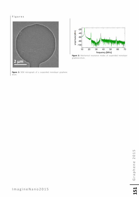
I m a g i n e N a n o 2 0 1 5
Gr
ap
he
ne
20
15
151
F i g u r e s
Figure 1: SEM micrograph of a suspended monolayer graphene drum.
Figure 2: Mechanical resonance modes of suspended monolayer graphene drum.

I m a g i n e N a n o 2 0 1 5
Gr
ap
he
ne
20
15
152
G r a p h e n e a p p l i c a t i o n s – B e y o n d t h e s t i c k y t a p e Knowledge Exchange Fellow, National Graphene Institute The University of Manchester, UK
Graphene - the so called "wonder material" could change the world with what seems endless applications and capabilities. Challenges exist in achieving this commercialisation and a key will be the creation of partnerships and collaborations to make these real from structures, to membranes and electronic applications. The National Graphene Institute (NGI) will house state of the art instruments and techniques to characterize graphene and to work with graphene and other 2D materials. The NGI will also collaborate on research projects with industry leaders. The building is specifically designed for industry to come and collaborate on academic research in order to push for the commercialization of Graphene enabling industry to work hand in hand with academics, and gain access to the science and the expertise it has to offer. The university is also focusing on a variety on Graphene applications such as electronics, membranes and coatings, energy storage, composition structure, the standard characterization of graphene, and Bio- Medical application.
F i g u r e s
Ania Servant

I m a g i n e N a n o 2 0 1 5
Gr
ap
he
ne
20
15
153
G r o w t h M e c h a n i s m o f H e x a g o n a l B o r o n N i t r i d e : b y N a n o c r y s t a l l i n e G r a p h e n e A s s i s t a n c e a n d / o r b y B - N m o l e c u l a r d i f f u s i o n 1 Device Lab., Samsung Advanced Institute of Technology, Suwon 443-801 Republic of Korea 2School of Advanced Materials Science and Engineering, SKKU Advanced Institute of Nanotechnology (SAINT), Sungkyunkwan University (SKKU), Suwon 440-746 Republic of Korea
Hexagonal boron nitride (h-BN) has received a great deal of attention as a substrate material for high-performance graphene electronics because it has an atomically smooth surface, lattice constant similar to that of graphene, large optical phonon modes, and a large electrical band gap. Herein, we discuss In the first part, we report the large scale synthesis of high-quality h-BN nanosheets in a chemical vapor deposition (CVD) process by controlling the surface morphologies of the copper (Cu) catalysts [1]. It was found that morphology control of the Cu foil is much critical for the formation of the pure h-BN nanosheets as well as the improvement of their crystallinity. We demonstrate the performance enhancement of CVD based graphene devices with large-scale h-BN nanosheets. The mobility of the graphene device on the h-BN nanosheets was increased 3 times compared to that without the h-BN nanosheets. The on-off ratio of the drain current is 2 times higher than that of the graphene device without h-BN. We can determine occasionally nanocrystalline graphene (nc-G) on Cu foil during h-BN growth process. Unintentionally formed nanocrystalline graphene (nc-G) can act as a useful seed for the large-area synthesis of hexagonal boron nitride (h-BN) nanosheets with an atomically flat surface that is comparable to that of exfoliated single crystal h-BN. A wafer-scale dielectric h-BN nanosheets was successfully synthesized on a bare sapphire substrate by assistance of nc-G without metal catalyst [2]. We systematically discuss the growth mechanism of these nc-G-tailored h-BN nanosheets in the second part.
Until now, because of the low solubility of N atoms in metals, hexagonal boron nitride (h-BN) growth has explained by surface reaction on metal rather than by penetration/precipitation of B and N atoms in metal. In the third part, we present an impressive pathway of h-BN formation at the interface between Ni and oxide substrate based on B-N molecular diffusion into Ni through individual atomic vacancies [3]. First-principles calculations confirmed the formation energies of the h-BN layers on and under the metal and the probability of B-N molecular diffusion in metal. The interface growth behavior depends on the species of metal catalysts, and these simulation results well support experimental results. These approaches provide a novel method for preparing high-quality two-dimensional materials on a large surface. R e f e r e n c e s [1] Kang Hyuck Lee, Hyeon-Jin Shin, Jinyeong Lee,
In-yeal Lee, Gil-Ho Kim, Jae-Young Choi, and Sang-Woo Kim, Nano Lett., 12 (2), 714-718 (2012).
[2] Kang Hyuck Lee, Hyeon-Jin Shin, Brijesh Kumar, Han Sol Kim, Jinyeong Lee, Ravi Bhatia, Sang-Hyeob Kim, In-Yeal Lee, Hyo Sug Lee, Gil-Ho Kim, Ji-Beom Yoo, Jae-Young Choi and Sang-Woo Kim, Angew. Chem. Int. Edi. 53 (43), 11493-11497 (2014).
[3] Seongjun Park, Jinyeong Lee, Han Sol Kim, Jong-Bong Park, Kang Hyuck Lee, Sang A Han, Sungwoo Hwang, Sang-Woo Kim and Hyeon-Jin Shin, ACS Nano, online published.
Hyeon-Jin Shin1, Seongjun Park1, Kang
Hyuck Lee2, Jinyeong Lee2, Sang-Woo Kim2

I m a g i n e N a n o 2 0 1 5
Gr
ap
he
ne
20
15
154
F i g u r e s

I m a g i n e N a n o 2 0 1 5
Gr
ap
he
ne
20
15
155
S T M a n d N C - A F M i n v e s t i g a t i o n s o f G r a p h e n e o n M e t a l S u r f a c e s 1 SPECS Surface Nano Analysis GmbH, Voltastrasse. 5, 13355 Berlin, Germany
We present recently obtained results in graphene-based systems as measured with STM and NC-AFM techniques. We highlight the latest state-of-the-art developments in these two techniques and show how these techniques are applied in the latest graphene research as well in other experimental systems. The SPM Aarhus 150 is an ideal instrument for investigating lattice mismatched surfaces, with a focus in the present talk of SPM measurements on the graphene/Ir(111) system [1]. Microscopy experiments were performed in constant current / constant frequency shift (CC/CFS) and constant height (CH) modes, exploiting a combination of the STM and NC-AFM capabilities of the system. We found that in STM imaging the electronic contribution is prevailing compared to the topographic one and the inversion of the contrast can be assigned to the particular features in the electronic structure of graphene on Ir(111). Contrast changes observed in constant height AFM measurements [1] are analyzed on the basis of the energy, force, and frequency shift curves, obtained in DFT calculations, reflecting the interaction of the W-tip with the surface and are attributed to the difference in the height and the different interaction strength for high-symmetry cites within the moirè unit cell of graphene on Ir(111).The presented findings are of general importance for the understanding of the properties of the lattice-
mismatched graphene/metal systems especially with regard to possible applications as templates for molecules or clusters. R e f e r e n c e s [1] E. N. Voloshina et al., Nature Sci. Rep. 3, 1072
(2013). F i g u r e s
Figure 1: Gr/Ir(111) moirés (left) are contrasted with STM/NC-AFM measurements, with feedback switched ‘on-the-fly’ (right) at tunnelling voltages of +0.46 (top-right) and -0.2 V (bottom-right). The top of each image demonstrates the effect of feedback via tunnelling current and the bottom feedback in NC-AFM modeshows STM, the bottom Δf (AFM)
V. Simic-Milosevic, Y. Dedkov, A. Kaiser, S. Schmitt, S. Bahr, O. Schaff, A. Thissen

I m a g i n e N a n o 2 0 1 5
Gr
ap
he
ne
20
15
156
E x t r a o r d i n a r y p h o t o l u m i n e s c e n c e i n U V / o z o n e t r e a t e d g r a p h e n e f l a k e s 1 Department of Physics and Astronomy, Shanghai Jiao Tong University, Shanghai 200240, China 2 State Key Laboratory of Functional Materials for Informatics, Shanghai Institute of Microsystem and Information Technology, Chinese Academy of Sciences, Shanghai 200050, China 3 Department of Physics, Southeast University, Nanjing 211189, China
Photoluminescence (PL) originating from two dimensional materials is attracting intense attention due to emergence of graphene and other direct bandgap materials like phosphorene and monolayer MoS2/WS2 [1-3]. In 2013, H. R. Gutiérrez et. al. observed extraordinary PL from edges of the chemically grown triangular WS2 and MoS2 monolayer flakes [2]. They proposed that the edge structure and chemistry of as-grown monolayer WS2/MoS2 are crucial for localized PL enhancement even though the actual mechanism leading to the edge-enhanced PL is still to be determined. Different from direct-bandgap monolayer metal dichalcogenides, luminescent graphene-based nanostructures usually have two distinct characteristics, i.e., shrinking nanometer scale structures and adsorbed surface chemical functional groups [1,4]. Aside from regular chemical synthesis routes, realizing in-situ PL in high-quality graphene flakes is significant in the future photonic and optoelectronic applications [1]. As previously reported, UV/ozone photochemical oxidation has a unique capability of carving few layer graphene (FLG) into about one nanometer deep patterns [4,5]. In this talk, we present extraordinary PL imaged by a confocal laser scanning microscope (CLSM) in the suspended and edge area of UV/ozone treated FLG flakes [Fig. 1]. Atomic force microscopy (AFM) and confocal Raman spectroscopy analyses [Fig. 2] indicate that monolayer graphene, the most adequate for characterizing ozonation, turn into some isolated amorphous nano-dots with an average size of ~20 nm. In addition, no obvious topographic difference can be detected between the suspended and Si/SiO2 (300 nm) supported FLG. X-ray photoelectron spectroscopy (XPS) results [Fig. 3] indicate a minute amount of luminescent-inducing
surface chemical groups are created after the ozonation. We think the properly etched nanostructures and luminescent-inducing surface chemical groups contribute together to the PL in FLG. However, the subjacent intact carbon layers and charge impurities resided in SiO2 substrate can cause severe PL quenching, and as a consequence result in non-detectable PL in the mono-/bilayer graphene and substrate supported FLG [6]. Our results deviate from report by Gokus et al. that they could detect PL only in monolayer graphene flakes instead of in FLG after oxygen plasma treatment [1]. We conclude the simultaneously ozonized graphene bottom layers, which are ascertained by high temperature vacuum annealing process, can efficiently decrease PL quenching and facilitate PL detection in the suspended and edge area of FLG. Our work may shed light on the understanding of luminescent two dimensional materials as well as contribute to building graphene-based nanophotonics and optoelectronics. R e f e r e n c e s [1] T. Gokus, R. R. Nair, A. Bonetti, M. Böhmler, A.
Lombardo, K. S. Novoselov, A. K. Geim, A. C. Ferrari, and A. Hartschuh, ACS Nano 3, 3963 (2009).
[2] H. R. Gutiérrez, N. P.-López, A. L. Elías, A. Berkdemir, B. Wang, R. Lv, F. L.-Urías, V. H. Crespi, H. Terrones, and M. Terrones, Nano Lett. 13, 3447 (2013).
[3] S. Zhang, J. Yang, R. Xu, F. Wang, W. Li, M. Ghufran, Y.-W. Zhang, Z. Yu, G. Zhang, Q. Qin, and Y. Lu, ACS Nano 8, 9590 (2014).
[4] N. Leconte, J. Moser, P. Ordejón, H. Tao, A. Lherbier, A. Bachtold, F. Alsina, C. M.
Haihua Tao1, Ziyu Zhang1, Hao Li1,
Guqiao Ding2, Zhenhua Ni3, Xianfeng Chen1
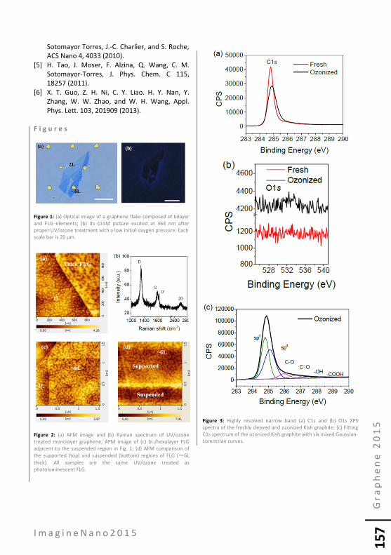
I m a g i n e N a n o 2 0 1 5
Gr
ap
he
ne
20
15
157
Sotomayor Torres, J.-C. Charlier, and S. Roche, ACS Nano 4, 4033 (2010).
[5] H. Tao, J. Moser, F. Alzina, Q. Wang, C. M. Sotomayor-Torres, J. Phys. Chem. C 115, 18257 (2011).
[6] X. T. Guo, Z. H. Ni, C. Y. Liao. H. Y. Nan, Y. Zhang, W. W. Zhao, and W. H. Wang, Appl. Phys. Lett. 103, 201909 (2013).
F i g u r e s
Figure 1: (a) Optical image of a graphene flake composed of bilayer and FLG elements; (b) its CLSM picture excited at 364 nm after proper UV/ozone treatment with a low initial oxygen pressure. Each scale bar is 20 μm.
Figure 2: (a) AFM image and (b) Raman spectrum of UV/ozone treated monolayer graphene; AFM image of (c) bi-/hexalayer FLG adjacent to the suspended region in Fig. 1; (d) AFM comparison of the supported (top) and suspended (bottom) regions of FLG (~6L thick). All samples are the same UV/ozone treated as photoluminescent FLG.
Figure 3: Highly resolved narrow band (a) C1s and (b) O1s XPS spectra of the freshly cleaved and ozonized Kish graphite; (c) Fitting C1s spectrum of the ozonized Kish graphite with six mixed Gaussian- Lorentzian curves.
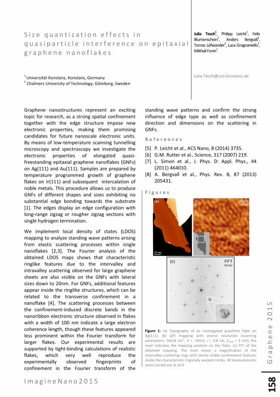
I m a g i n e N a n o 2 0 1 5
Gr
ap
he
ne
20
15
158
S i z e q u a n t i z a t i o n e f f e c t s i n q u a s i p a r t i c l e i n t e r f e r e n c e o n e p i t a x i a l g r a p h e n e n a n o f l a k e s 1 Universität Konstanz, Konstanz, Germany 2 Chalmers University of Technology, Göteborg, Sweden
Graphene nanostructures represent an exciting topic for research, as a strong spatial confinement together with the edge structure impose new electronic properties, making them promising candidates for future nanoscale electronic units. By means of low-temperature scanning tunnelling microscopy and spectroscopy we investigate the electronic properties of elongated quasi-freestanding epitaxial graphene nanoflakes (GNFs) on Ag(111) and Au(111). Samples are prepared by temperature programmed growth of graphene flakes on Ir(111) and subsequent intercalation of noble metals. This procedure allows us to produce GNFs of different shapes and sizes exhibiting no substantial edge bonding towards the substrate [1]. The edges display an edge configuration with long-range zigzag or rougher zigzag sections with single hydrogen termination.
We implement local density of states (LDOS) mapping to analyze standing wave patterns arising from elastic scattering processes within single nanoflakes [2,3]. The Fourier analysis of the obtained LDOS maps shows that characteristic ringlike features due to the intervalley and intravalley scattering observed for large graphene sheets are also visible on the GNFs with lateral sizes down to 20nm. For GNFs, additional features appear inside the ringlike structures, which can be related to the transverse confinement in a nanoflake [4]. The scattering processes between the confinement-induced discrete bands in the nanoribbon electronic structure observed in flakes with a width of 100 nm indicate a large electron coherence length, though these features appeared less prominent within the Fourier transform for larger flakes. Our experimental results are supported by tight-binding calculations of realistic flakes, which very well reproduce the experimentally observed fingerprints of confinement in the Fourier transform of the
standing wave patterns and confirm the strong influence of edge type as well as confinement direction and dimensions on the scattering in GNFs.
R e f e r e n c e s
[5] P. Leicht et al., ACS Nano, 8 (2014) 3735. [6] G.M. Rutter et al., Science, 317 (2007) 219. [7] L. Simon et al., J. Phys. D: Appl. Phys., 44
(2011) 464010. [8] A. Bergvall et al., Phys. Rev. B, 87 (2013)
205431.
F i g u r e s
Figure 1: (a) Topography of an investigated graphene flake on Ag(111). (b) QPI mapping with atomic resolution (scanning parameters: 54x54 nm2, V = -10mV, I = 0.8 nA, Vmod = 3 mV), the inset indicates the mapping position on the flake. (c) FFT of the obtained mapping. The inset shows a magnification of the intervalley scattering rings with clearly visible confinement features inside the characteristic trigonally warped circles. All measurements were carried out at 10 K
Julia Tesch1, Philipp Leicht1, Felix
Blumenschein1, Anders Bergvall2, Tomas Löfwander2, Luca Gragnaniello1, Mikhail Fonin1

I m a g i n e N a n o 2 0 1 5
Gr
ap
he
ne
20
15
159
S p i n D y n a m i c s i n H i g h - Q u a l i t y G r a p h e n e : R o l e o f E l e c t r o n - H o l e P u d d l e s a n d S p i n - P s e u d o s p i n C o u p l i n g 1 ICN2 - Institut Catala de Nanociencia i Nanotecnologia, Campus UAB, 08193 Bellaterra (Barcelona), Spain 2 Department of Physics, Universitat Autónoma de Barcelona, Campus UAB, 08193 Bellaterra, Spain 3 Institute for Materials Science and Max Bergmann Center of Biomaterials, Technische Universität Dresden, 01062 Dresden, Germany 4 ICREA, Institució Catalana de Recerca i Estudis Avancats, 08070 Barcelona, Spain
We report a strong spin dephasing effect induced by electron-hole puddles [1, 2] and spin-pseudospin coupling in ultraclean graphene, with long mean free path and uniform Rashba spin-orbit coupling as low as a few tens of µeV [3] . From the time dependence of spin dynamics of propagating wave packets, spin relaxation times typically on the order of few hundreds of picoseconds to the nanosecond scale are extracted, depending on the substrate-induced electron-hole characteristics. The energy dependence of spin relaxation times [4], together with the obtained ratio for spins pointing out-of-plane to spins in-plane (
/∥),
and scaling of spin lifetimes with disorder provide a consistent description of fundamentals of spin lifetimes [5] in the ultraclean grapheme limit. R e f e r e n c e s [1] J. Martin et al., Nature Physics 4, 144-148
(2008). [2] Y. Zhang et al., Nature Physics 5, 722 (2009). [3] C. R. Ast and I. Gierz, Phys. Rev. B 86, 085105
(2012) [4] Dinh Van Tuan, Frank Ortmann, David Soriano,
Sergio O. Valenzuela and Stephan Roche, Pseudospindriven spin relaxation mechanism in graphene. Nature Physics 10, 857-863 (2014).
[5] Dinh Van Tuan, Frank Ortmann, Aron W. Cummings, David Soriano, Sergio O. Valenzuela and Stephan Roche, Spin Dynamics in High-Quality Graphene: Role of Electron-Hole Puddles and Spin-Pseudospin Coupling. Submitted to Phys. Rev. Lett.
F i g u r e s
Figure 1: Spin polarizations for out-of-plane (a) and in-plane (b) spin injections. (c): Illustration of parallel (green) and perpendicular (violet) components. The projection of parallel component in x direction is shown in blue.
Figure 2: Time-dependent spin polarization for in- plane and out-of-plane polarized wavepacket in grapheme on hBN and SiO2 substrates. Inset: Onsite energy distribution of the carbon atoms in the graphene sample, which mimics the chemical potential induced by hBN (green) and SiO2 (black) substrates together with their Gaussian fitting lines.
Dinh Van Tuan1,2
, Frank Ortmann1,3, Aron W. Cummings1, David Soriano1, Sergio O. Valenzuela1,4 and Stephan Roche1,4

I m a g i n e N a n o 2 0 1 5
Gr
ap
he
ne
20
15
160
G r a p h e n e T r a n s i s t o r s f o r D e t e c t i o n o f N e u r o n a l A c t i v i t y 1 Institut Néel, CNRS, 25 Rue des Martyrs, 38042 Grenoble, France 2 Université Grenobel Alpes, HP2 & INSERM U1042, 38041 Grenoble, France
Due to its outstanding properties graphene offers an ideal platform for sensing and culturing neural networks. Its biocompatible, soft, and chemically inert nature associated to the lack of dangling bonds offers novel perspectives for direct integration in bioelectric probes. The presence of readily accessible surface charges gives the unprecedented possibility to realize a strong electrical coupling with cells. Moreover, the possibility to transfer it on transparent and flexible substrates opens the way to a variety of applications for in-vitro studies and in-vivo implants with reduced inflammatory response [1]. Here we present a study of our CVD grown SL graphene [2] with regard to its biocompatibility and bioelectrical interfacing. We found, that while on any other substrate an adhesive coating (such as polyL-lysine) is needed to assure neuronal growth in culture, graphene actively promotes the growth even without a coating. Moreover, in comparison to other frequently used substrates the neuron density and the neurite length are significantly higher for neurons cultured on uncoated graphene as shown in Fig. 1. Further, in order to prove the ability of graphene based devices to detect neuronal signals, we realized graphene FET arrays on Si/SiO2, glass and polyimide substrates and performed characterization measurements in cell culture medium with a Pt gate electrode. To mimic the neuronal spiking we superimposed 1ms long Gaussian pulses on the DC offset of the Pt-electrode. All graphene FETs showed reproducible electrical properties with a mobility around 6000
cm2V
-1s
-1 and a sensitivity to potential changes up to 2 mS/V allowing a rapid detection of very small (around 200µV) potential spikes comparable with
neuronal signaling [3]. Also, neurons were shown to survive on graphene FETs for periods up to 19-21 days achieving the regular maturation stage. In conclusion, our studies show the enormous potential of graphene based devices as neuronal growth support and bioelectrical sensors R e f e r e n c e s [1] V.S. Polikov, P.A. Tresco, W.M. Reichert,
Journal of Neuroscience Methods 148 (2005) 1–18.
[2] Z. Han, A. Kimoche, D. Kalita, A. Allain, H. Arjmandi-Tash, A. Reserbat-Plantey, L. Marty, S. Pairis, N. Bendiab, J. Coraux, V. Bouchiat, Adv. Func. Mat., 24 (2014) 964-970.
[3] J.J. Pancrazio, J.C. Keefer, W. Ma, D.A. Stenger, G.W. Gross, NeuroToxicology, 22 (2001) 393-400.
F i g u r e s
Figure 1: Coating-free graphene promotes neuronal growth. a) Coating-free glass and graphene with neurons after 4 days in culture. The neurons survive only on graphene. b) Neuron density on day 1 and day 2 of and c) the average neurite length on day 2 of culture on different substrates: Ctrl - glass control sample, Gr - graphene, Gr-noPLL – coating-free graphene, Par-C – parylene-C and PI – polyimide.
Farida Veliev1, A. Briancon-Marjollet2,
A. Bourrier1 , D. Kalita1, V. Bouchiat1 and C. Delacour1
I m a g i n e N a n o 2 0 1 5
Gr
ap
he
ne
20
15
161
Figure 2: Graphene FET characteristics. a) Optical micrograph of a typical device. b) Conductance variation (black line) and device sensitivity (red line) as function of front liquid gate potential measured in cell culture medium. c) Detection of 1 ms long 250 µV Gaussian potential spike applied to the medium through a Pt-electrode using graphene FET.
I m a g i n e N a n o 2 0 1 5
Gr
ap
he
ne
20
15
162
N a n o g r a p h e n e o x i d e - c e l l i n t e r a c t i o n s a n d i t s p o t e n t i a l f o r t u m o r d e s t r u c t i o n 1 Nanotechnology Research Division-TEMA, Mechanical Engineering Dpt University of Aveiro, 3810-193 Aveiro, Portugal 2 Department of Biochemistry and Molecular Biology I Faculty of Chemistry, Universidad Complutense, 28040-Madrid, Spain 3 Department of Inorganic and Bioinorganic Chemistry Faculty of Pharmacy, Universidad Complutense, 28040-Madrid, Spain 4 Networking Research Center on Bioengineering, Biomaterials and Nanomedicine CIBER-BBN, Spain
Many applications of graphene in the area of bio and nanomedicine have been proposed and it is important to review its potential with a fine-tooth comb with two main specific objectives: to evaluate if it could possess all the parameters that make a material suitable for its use on the human body, and to specify conditions, applications and materials modifications that could assure materials biocompatibility and a positive biological response. For example, one of the most novel fields of nanomedicine applied to cancer research is using nanoparticles (NPs) but their application will not be feasible without a previous understanding of NPscell/tissue interactions, possible toxicity and accumulation risks. [1] These cancer therapies work through the NPs preferential accumulation in cancerous tissue after intravenous injection due to the combination of leaky vasculature and poor lymphatic drainage which results in what is known as the enhanced and permeability retention effect (EPR). Simultaneously, among the new arising therapies, the hyperthermia of tumours has been investigated as a minimally invasive alternative to surgery that can induce lethal damage to cellular components at temperatures above 40 ºC. Unfortunately, simple heating techniques have trouble discriminating between tumours and surrounding healthy tissues. Thus, by the combination of these two concepts, the localized nanoparticle-based hyperthermia raised as a powerful and potential treatment on its own. Amongst hyperthermia potential agents, nano graphene oxide (nGO) has been proposed due to its strong Near-Infrared (NIR 700-1100 nm range) optical absorption ability and its unique 2-dimensional aspect ratio. [3] Restricting all dimensions at nanoscale could allow unique
performing when compared to any other nanoparticle, but it is mandatory to deeply study the hyperthermia route and the kind of nGO-cell interactions induced in the process. By optimizing the nGO synthesis, it is possible to diminish the initial cell-particle interactions to reduce possible future toxicity in healthy cells.[4] nGO cell exposure and its influence on both the innate and the adaptive immune responses was evaluated in murine lymphocytes and there was no stimulation of proinflammatory cytokine secretion assuring a good biocompatibility. [5] Moreover, the nGO incorporation kinetics and mechanisms by different cell types either in the absence or in the presence of eight endocytosis inhibitors showed that macropynocitosis is the general mechanism of nGO internalization, but that it can also entry through clathrin-dependent mechanisms in hepatocytes and macrophages. [6] This fact gives light to which will be the key surface factors in a future design of targeted delivery of this NPs by means of active moieties. Cell internalization kinetics were established for producing a safe and efficient tumor cell destruction avoiding damage on untreated cells as well as an evaluation of the nature of tumor destruction that could be produced by this hyperthermia treatment.The type of cell damage and toxicity produced by NIR laser irradiation was evaluated as a function of exposure time and laser power in order to control the temperature rise and consequent damage in the nGO containing cell culture medium. The results suggested that controlling the type of cell death, the threshold for producing soft or harmful damage could be precisely ontrolled and so, the increase of
M. Vila1,3,4, , M. C. Matesanz2 , G.
Gonçalves1 , M. J. Feito2, J. Linares2,P.A.A.P. Marques1, , M.T. Portolés2, M.Vallet-Regic4

I m a g i n e N a n o 2 0 1 5
Gr
ap
he
ne
20
15
163
cytokine release to the medium, having this a direct impact on immune system reactions.[7] R e f e r e n c e s [1] Day ES, Morton JG, West JL. J Biomed Eng
2009 ;131:074001. [2] Yang K, Wan J, Zhang et al. ACS Nano
2011;5:516-22. [3] Gonçalves G, Vila M, et al. Adv. Healthcare
Materials. 2013; 2(8):1072. [4] Vila M, Portolés MT, Marques PAAP, Feito et
al. Nanotechnology 2012; 23:465103. [5] MJ. Feito, M. Vila , MC. Matesanz et al J
Colloid Interface Science 2014; 432, 221. [6] J.Linares, M. C. Matesanz, M. Vila et al ACS
applied materials & interfaces 2014; 27,13697. [7] Vila M, Matesanz MC, Gonçalves G, et al.
Nanotechnology 2014 (25) 035101.
F i g u r e s
Figure 1: Morphology evaluation by confocal microscopy of cultured human Saos-2 osteoblasts in the presence of GOs, before (left) and after 7 min of 1.5 W/cm2 laser irradiation showing necrotic cells (right).
.

I m a g i n e N a n o 2 0 1 5
Gr
ap
he
ne
20
15
164
T w i s t - c o n t r o l l e d r e s o n a n t t u n n e l l i n g i n g r a p h e n e / b o r o n - n i t r i d e / g r a p h e n e h e t e r o s t r u c t u r e s Department of Physics, Lancaster University, Lancaster, LA1 4YB, UK
Recent developments in van der Waals heterostructures made from stacks of two-dimensional crystals have already led to the observation of new physical phenomena, such as the metal-insulator transition and Coulomb drag, and to the realisation of functional devices, such as tunnel diodes, and tunnel transistors. An unprecedented degree of control of the electronic properties is available not only by means of the selection of materials in the stack, but also by adjusting the relative orientation of the component layers. In this talk I shall discuss how careful alignment of the crystallographic orientation of two graphene electrodes, separated by a layer of hexagonal boron nitride (hBN) in a transistor device, can achieve resonant tunnelling with conservation of electron energy, momentum and, potentially, chirality [1]. This leads to resonance peaks and negative differential conductances in the device characteristics, which, in turn, can be used to induce a tuneable radio-frequency oscillatory current. Also, the application of a magnetic field in the plane of the two graphene layers can be used to reveal the effects of graphene's chirality on the tunnelling current, and may lead to valley polarised currents. Finally, I note that the momentum and velocity distribution of the tunnelling electrons is highly anisotropic, which may lead to interesting effects in a ballistic device. R e f e r e n c e s [1] A. Mishchenko, J. S. Tu, Y. Cao, R. V.
Gorbachev, J. R. Wallbank, M.T. Greenaway, V. E. Morozov, S. V. Morozov, M. J. Zhu, S. L. Wong, F. Withers, C. R. Woods, Y.-J. Kim, K.
Watanabe, T. Taniguchi, E. E. Vdovin, O. Makarovsky, T. M. Fromhold, V. I. Falko, A. K. Geim, L. Eaves, K. S. Novoselov, Nature Nanotechnology 9, 808 (2014) D. Weiss et al., Phys. Rev. Lett. 66, 2790 (1991).
F i g u r e s
Figure 1: (a) The measured (solid curve) and theoretically calculated (dashed curve) tunnelling currents, displaying the resonant peak at a bias voltage of Vb≈0.8V. (b-d) The conditions of energy and momentum conservation, which enable the tunnelling of Dirac electrons, are visualized in the left panels by the line of intersection (red) of the Dirac cones in the two graphene layers. The shift of these in momentum is set by the misalignment of the Brillouin zones of the two graphene layers (see inset of (a)), while the displacement along the energy axis is controlled by the applied bias voltage. Importantly, panel (c) displays the conditions for which the main resonant peak occurs. The tunneling probability for an electron is also modulated by the interference between the electron amplitudes on graphene's A/B carbon sites (right panels).
AJ. R. Wallbank, A. Mishchenko, J.S. Tu, Y. Cao, R.V. Gorbachev, M.T. Greenaway, V.E. Morozov, S.V.Morozov, M.J. Zhu, S.L. Wong, F. Withers, C.R. Woods, Y.-J. Kim, K. Watanabe, T. Taniguchi, E.E. Vdovin, O. Makarovsky, T.M. Fromhold, V.I. Falko, A.K. Geim, L.Eaves, K.S. Novoselov
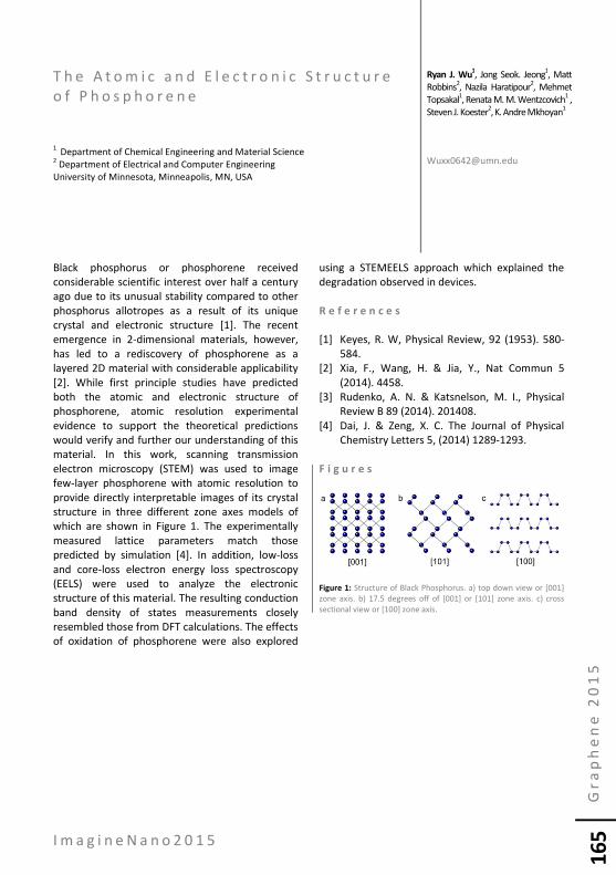
I m a g i n e N a n o 2 0 1 5
Gr
ap
he
ne
20
15
165
T h e A t o m i c a n d E l e c t r o n i c S t r u c t u r e o f P h o s p h o r e n e 1 Department of Chemical Engineering and Material Science 2 Department of Electrical and Computer Engineering University of Minnesota, Minneapolis, MN, USA
Black phosphorus or phosphorene received considerable scientific interest over half a century ago due to its unusual stability compared to other phosphorus allotropes as a result of its unique crystal and electronic structure [1]. The recent emergence in 2-dimensional materials, however, has led to a rediscovery of phosphorene as a layered 2D material with considerable applicability [2]. While first principle studies have predicted both the atomic and electronic structure of phosphorene, atomic resolution experimental evidence to support the theoretical predictions would verify and further our understanding of this material. In this work, scanning transmission electron microscopy (STEM) was used to image few-layer phosphorene with atomic resolution to provide directly interpretable images of its crystal structure in three different zone axes models of which are shown in Figure 1. The experimentally measured lattice parameters match those predicted by simulation [4]. In addition, low-loss and core-loss electron energy loss spectroscopy (EELS) were used to analyze the electronic structure of this material. The resulting conduction band density of states measurements closely resembled those from DFT calculations. The effects of oxidation of phosphorene were also explored
using a STEMEELS approach which explained the degradation observed in devices. R e f e r e n c e s [1] Keyes, R. W, Physical Review, 92 (1953). 580-
584. [2] Xia, F., Wang, H. & Jia, Y., Nat Commun 5
(2014). 4458. [3] Rudenko, A. N. & Katsnelson, M. I., Physical
Review B 89 (2014). 201408. [4] Dai, J. & Zeng, X. C. The Journal of Physical
Chemistry Letters 5, (2014) 1289-1293. F i g u r e s
Figure 1: Structure of Black Phosphorus. a) top down view or [001] zone axis. b) 17.5 degrees off of [001] or [101] zone axis. c) cross sectional view or [100] zone axis.
Ryan J. Wu1, Jong Seok. Jeong1, Matt
Robbins2, Nazila Haratipour2, Mehmet Topsakal1, Renata M. M. Wentzcovich1 , Steven J. Koester2, K. Andre Mkhoyan1
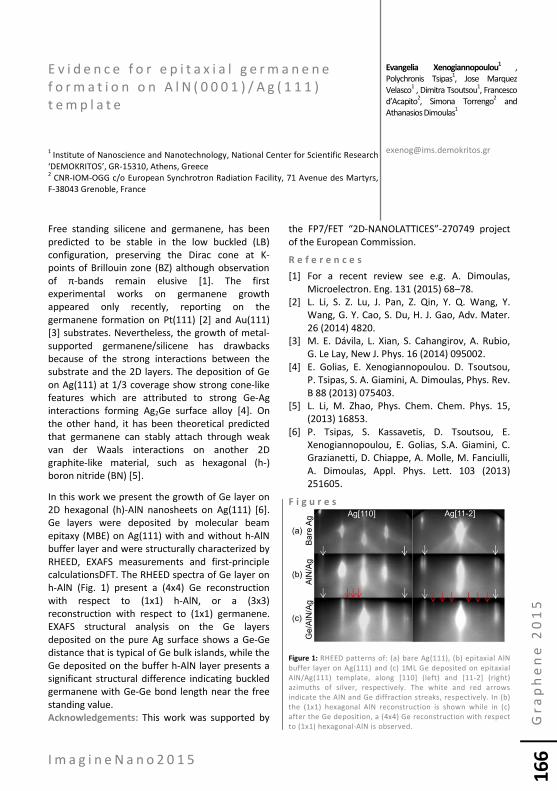
I m a g i n e N a n o 2 0 1 5
Gr
ap
he
ne
20
15
166
E v i d e n c e f o r e p i t a x i a l g e r m a n e n e f o r m a t i o n o n A l N ( 0 0 0 1 ) / A g ( 1 1 1 ) t e m p l a t e 1 Institute of Nanoscience and Nanotechnology, National Center for Scientific Research ‘DEMOKRITOS’, GR-15310, Athens, Greece 2 CNR-IOM-OGG c/o European Synchrotron Radiation Facility, 71 Avenue des Martyrs, F-38043 Grenoble, France
Free standing silicene and germanene, has been predicted to be stable in the low buckled (LB) configuration, preserving the Dirac cone at K-points of Brillouin zone (BZ) although observation of π-bands remain elusive [1]. The first experimental works on germanene growth appeared only recently, reporting on the germanene formation on Pt(111) [2] and Au(111) [3] substrates. Nevertheless, the growth of metal-supported germanene/silicene has drawbacks because of the strong interactions between the substrate and the 2D layers. The deposition of Ge on Ag(111) at 1/3 coverage show strong cone-like features which are attributed to strong Ge-Ag interactions forming Ag2Ge surface alloy [4]. On the other hand, it has been theoretical predicted that germanene can stably attach through weak van der Waals interactions on another 2D graphite-like material, such as hexagonal (h-) boron nitride (BN) [5].
In this work we present the growth of Ge layer on 2D hexagonal (h)-AlN nanosheets on Ag(111) [6]. Ge layers were deposited by molecular beam epitaxy (MBE) on Ag(111) with and without h-AlN buffer layer and were structurally characterized by RHEED, EXAFS measurements and first-principle calculationsDFT. The RHEED spectra of Ge layer on h-AlN (Fig. 1) present a (4x4) Ge reconstruction with respect to (1x1) h-AlN, or a (3x3) reconstruction with respect to (1x1) germanene. EXAFS structural analysis on the Ge layers deposited on the pure Ag surface shows a Ge-Ge distance that is typical of Ge bulk islands, while the Ge deposited on the buffer h-AlN layer presents a significant structural difference indicating buckled germanene with Ge-Ge bond length near the free standing value. Acknowledgements: This work was supported by
the FP7/FET “2D-NANOLATTICES”-270749 project of the European Commission.
R e f e r e n c e s
[1] For a recent review see e.g. A. Dimoulas, Microelectron. Eng. 131 (2015) 68–78.
[2] L. Li, S. Z. Lu, J. Pan, Z. Qin, Y. Q. Wang, Y. Wang, G. Y. Cao, S. Du, H. J. Gao, Adv. Mater. 26 (2014) 4820.
[3] M. E. Dávila, L. Xian, S. Cahangirov, A. Rubio, G. Le Lay, New J. Phys. 16 (2014) 095002.
[4] E. Golias, E. Xenogiannopoulou. D. Tsoutsou, P. Tsipas, S. A. Giamini, A. Dimoulas, Phys. Rev. B 88 (2013) 075403.
[5] L. Li, M. Zhao, Phys. Chem. Chem. Phys. 15, (2013) 16853.
[6] P. Tsipas, S. Kassavetis, D. Tsoutsou, E. Xenogiannopoulou, E. Golias, S.A. Giamini, C. Grazianetti, D. Chiappe, A. Molle, M. Fanciulli, A. Dimoulas, Appl. Phys. Lett. 103 (2013) 251605.
F i g u r e s
Figure 1: RHEED patterns of: (a) bare Ag(111), (b) epitaxial AlN buffer layer on Ag(111) and (c) 1ML Ge deposited on epitaxial AlN/Ag(111) template, along [110] (left) and [11-2] (right) azimuths of silver, respectively. The white and red arrows indicate the AlN and Ge diffraction streaks, respectively. In (b) the (1x1) hexagonal AlN reconstruction is shown while in (c) after the Ge deposition, a (4x4) Ge reconstruction with respect to (1x1) hexagonal-AlN is observed.
Evangelia Xenogiannopoulou1 ,
Polychronis Tsipas1, Jose Marquez Velasco1 , Dimitra Tsoutsou1, Francesco d’Acapito2, Simona Torrengo2 and Athanasios Dimoulas1

I m a g i n e N a n o 2 0 1 5
Gr
ap
he
ne
20
15
167
S i l a n e - C a t a l y z e d S i n g l e - C r y s t a l l i n e G r a p h e n e G r o w t h o n H e x a g o n a l B o r o n N i t r i d e 1 State Key Laboratory of Functional Materials for Informatics, Shanghai Institute of Microsystem and Information Technology, Chinese Academy of Sciences, 865 Changning Road, Shanghai 200050, P.R. China 2 Division of Physics and Applied Physics, School of Physical and Mathematical Sciences, Nanyang Technological University, 21 Nanyang Link, Singapore 637371 3 Institute of Textiles and Clothing, Hong Kong Polytechnic University, Kowloon, Hong Kong, 999077, P. R. China
Hexagonal boron nitride (h-BN) is considered as an ideal substrate for graphene, on which superior graphene properties are demonstrated. Direct grapheme growth on h-BN by chemical vapor deposition (CVD) were already realized but with very low growth rate, because of the absence of catalyst. With extensive investigations, we discovered that silane, can serve as a gaseous catalyst, boosting the graphene growth rate by 2-3 orders of magnitude, yielding in single crystalline graphene domain size up to 20 μm, with more than 90% of the grains aligned precisely with the h-BN substrate. Preliminary results show that the
edges of grapheme can be tuned from pure armchair to pure zigzag. The results may stimulate further research on the graphene/h-BN hetero-structure and graphene/h-BN super-lattice, which may have profound impact on graphene research in the future. Most recent results on the CVD synthesis of single layered h-BN grains over 100 µm and inch-sized single crystal graphene wafer will also be briefly presented.
Shujie Tang1, Haomin Wang1, Ting Yu2, Feng Ding3 and Xiaoming Xie
1

I m a g i n e N a n o 2 0 1 5
Gr
ap
he
ne
20
15
168
G r o w t h a n d a t o m i c - s c a l e c h a r a c t e r i z a t i o n o f g r a p h e n e - h - B N h y b r i d s o n s i n g l e c r y s t a l s u b s t r a t e s Department of Materials Science and Engineering, College of Engineering; Center for Nanochemistry (CNC), Peking University, Beijing, China
We have performed systematic STM studies of the growth and the microscopic structure of graphene on Cu, Pt, Rh etc. foil substrates, and clarified their growth mechanisms along with the aid of traditional methods like Raman spectroscopy, scanning electron microscopy (SEM) and so on [4]. Interestingly, we found that randomly stacked bilayer or few layer segregated graphene on Rh foils usually exhibit various moiré patterns, on which angel-dependent van hove singularities was observed by STM/STS [5,6]. Moreover, we showed that h-BN, a structural analogue of graphene, can be patched onto graphene to form a monolayer hybrid on Rh(111). This hybrid formation was considered be promising for opening up a small band gap of graphene, and most of the efforts were performed by growing the sample on Cu foil substrates. In our work, we show that, on the deliberately selected Rh(111) and Ir(111) substrates with strong and weak interface interactions with graphene and h-BN, a monolayer hybrid of G-h-BN can be constructed with atomic scale continuity at their interfaces mostly with a preferred zigzag type, as identified by STM and also verified by DFT calculations. The influence of the substrates on the electronic properties of the two analogue materials were also presented.
R e f e r e n c e s [1] Y. F. Zhang, Z.F. Liu*, et al., et al., ACS Nano,
5(2011)4014. [2] Y.F. Zhang*, Z.F. Liu*, et al., ACS Nano
6(2012)10581. [3] Y. F. Zhang*, L. He*, et al., Phys. Rev. Lett.
109(2012)126801. [4] Y. F. Zhang*, Z. F. Liu*, et al., Nano Lett.
13(2013)3439. [5] Y. F. Zhang*, Z. F. Liu*, et al., Nano Lett.
14(2014)6342. F i g u r e s
Yanfeng Zhang

I m a g i n e N a n o 2 0 1 5
Gr
ap
he
ne
20
15
169
S w i t c h i n g o f M a g n e t o c r y s t a l l i n e A n i s o t r o p y o f a S i n g l e L a y e r C o b a l t F i l m b y G r a p h e n e SPINTEC, UMR CEA/CNRS/UJF-Grenoble 1/Grenoble-INP, INAC 38054 Grenoble, France
Two-dimensional graphene has demonstrated outstanding physical properties such as exceptional electrical, thermal, and mechanical properties [1,2], but also very long spin diffusion lengths at room temperature [3–7]. This offers an unprecedented platform for the advent of lateral spintronics. For instance, graphene interfaced with insulators/semiconductors (SiC, SiO2, Al2O3), magnetic insulator EuO [8,9], and magnetic metals have been intensively studied in recent years. Among many interesting phenomena which have been recently proposed for graphene/magnetic metal interfaces, perpendicular magnetic anisotropy (PMA) has been attracting much attention in a view of its general interest for spintronics. In particular, PMA has been reported in Co/graphene interface [10]. However, a single layer of Co film, either free standing or on substrates (e.g. Pt, Au, etc.), persists in-plane anisotropy and switching it to the out-of-plane one is a big challenge. In this work, we report graphene proximity induced switching of magnetocrystalline anisotropy of single layer Co film from the in-plane to out-of-plane orientation with a large PMA value comparable to thicker Co films. The calculations were performed in two steps using Vienna Ab-Initio Simulation Package (VASP), which is based on density functional theory with generalized gradient approximation (PBE), for the exchange correlation potential and projector augmented wave based pseudopotentials [11]. First, the structures are relaxed with no spin-orbit interaction taken into account for determining the most favorable adsorption geometry of graphene on Co. Then the spin-orbit coupling was included and the total energy of the system was determined as a function of the orientation of the magnetic moments. The 19×19×1 k-point mesh was used in
all calculations and the energy cutoff was set to 520 eV. The atomic structures were relaxed until the forces were smaller than 1 meV/Å. For the anisotropy calculations, the total energies were converged to with precision of 10-7 eV. First, the magnetocrystalline anisotropy of a free standing Co layer was calculated and found to be about -2.17 mJ/m2 favoring in-plane anisotropy. Next, we optimized one Co single layer on graphene sheet. Two high symmetric structures are considered: BC stacking (Co sitting on the center of hexagonal cell of graphene) and AB stacking (Co is placed on top of carbon atoms). We found that BC stacking is a semi-stable phase and it preserves the in-plane anisotropy with a bit larger absolute value of 2.23 mJ/m2. Interestingly, for the stable phase of AB stacking the anisotropy switches to out-of-plane direction with a value of 1.43 mJ/m2, which is comparable to thicker Co films. We find that the hybridization between C-pz and Co-dZ2 plays the crucial role in switching the anisotropy of Co film. At the same time, the Dirac point of graphene is also modified by Co presence. Acknowledgements: This work is supported by EU Future Emerging Technology Flagship "Graphene" and ANR NMGEM. R e f e r e n c e s [1] A. H. Castro Neto, et al., Rev. Mod. Phys. 8,
109 (2009). [2] A. K. Geim and K. S. Novoselov, Nat. Mater. 6,
183 (2007). [3] N. Tombros, C. Jozsa, M. Popinciuc, H. T.
Jonkman, and B. J. van Wees, Nature 448, 571 (2007).
Hongxin Yang and Mairbek Chshiev

I m a g i n e N a n o 2 0 1 5
Gr
ap
he
ne
20
15
170
[4] M. Popinciuc, et al., Phys. Rev. B 80, 214427 (2009).
[5] B. Dlubak, et al., Appl. Phys. Lett. 97, 092502 (2010).
[6] W. Han and R. K. Kawakami, Phys. Rev. Lett. 107, 047207 (2011).
[7] T.-Y. Yang, et al., Phys. Rev. Lett. 107, 047206 (2011).
[8] H. X. Yang, A. Hallal, D. Terrade, X. Waintal, S. Roche, and M. Chshiev, Phys. Rev. Lett. 110, 046603 (2013).
[9] A. G. Swartz, et al., ACS Nano 6, 10063 (2012). [10] Chi Vo-Van, Z. Kassir-Bodon, H.X. Yang, J.
Coraux, et al., New J. Phys. 12, 103040 (2010). [11] G. Kresse and J. Hafner, Phys. Rev. B 47, 558
(1993); G. Kresse and J. Furthmuller, Phys. Rev. B 54 (1996); P. E. Blochl, Phys. Rev. B 50, 17953 (1994).

I m a g i n e N a n o 2 0 1 5
Gr
ap
he
ne
20
15
171
V a l l e y a n d s p i n c u r r e n t s i n 2 D t r a n s i t i o n m e t a l d i c h a l c o g e n i d e s Department of Physics and Center of Theoretical and Computational Physics, The University of Hong Kong, Hong Kong, China
The recent emergence of two-dimensional transition metal dichalcogenides (TMDs) provides a new laboratory for exploring the internal quantum degrees of freedom of electrons for new electronics. These include the electron spin and the valley pseudospin that labels the degenerate band extrema in momentum space. In 2D TMDs, the valley pseudospin acquires physical properties which allow its quantum manipulations in ways similar to the control of spins, making possible valley-based electronics [1]. The generation and control of spin and valley pseudospin currents are at the heart of spin and valley based electronics. Two mechanisms will be discussed for generating spin and valley currents of electrons in 2D TMDs: (I) the valley and spin Hall current arising from the Berry curvatures [2]; and (II) the nonlinear valley and spin currents arising from Fermi pocket anisotropy [3]. The two effects have distinct scaling with the field and different dependence of the current direction on the field direction and crystalline axis. The nonlinear current response further allows two unprecedented possibilities to
generate pure spin and valley flows without net charge current, either by an AC bias or by an inhomogeneous temperature distribution [3]. This points to a new route towards electrical and thermal generations of spin and valley currents for spintronic and valleytronic applications. I will also discuss the valley Hall effect of charged excitons in monolayer TMDs arising from the exchange interaction between the electron and hole constituents of the exciton [4]. R e f e r e n c e s [1] X. Xu, W. Yao, D. Xiao and T. F. Heinz, Nature
Physics, 10 (2014) 343. [2] D. Xiao, G. Liu, W. Feng, X. Xu and W. Yao,
Physical Review Letters, 108 (2012) 196802. [3] H. Yu, Y. Wu, G. Liu, X. Xu and W. Yao, Physical
Review Letters, 113 (2014) 156603. [4] H. Yu, G. Liu, P. Gong, X. Xu and W. Yao,
Nature Communications, 5 (2014) 3876.
Wang Yao

I m a g i n e N a n o 2 0 1 5
Gr
ap
he
ne
20
15
172
A c t i v i t i e s o n S t a n d a r d i z a t i o n o f P r o p e r t i e s o f G r a p h e n e i n K o r e a SAINT (SKKU Advanced Institute of Nanotechnology) Sungkyunkwan University Suwon, Korea
Graphene with two dimensional honeycomb structures of carbon atoms is known as having exceptional electrical, thermal, and mechanical properties. Their applications are expected to be in high speed, flexible, and transparent devices. Research activities on graphene in Korea have been focused on commercialization of graphene based materials and devices. Activities of
standardization of graphene in Korea will be presented. Topics in standardization of graphene discussed are followings: Characterization of electrical properties of graphene, Evaluation of the number of layers of graphene, and Evaluation of domain boundaries of graphene. Other activities of standardization of carbon materials will be introduced as well.
Ji-Beom Yoo

I m a g i n e N a n o 2 0 1 5
Gr
ap
he
ne
20
15
173
I n s i t u T r a n s m i s s i o n E l e c t r o n M i c r o s c o p y f o r N a n o s c a l e D y n a m i c s a n d P r o p e r t i e s o f 2 D m a t e r i a l s 1 Center for Integrated Nanostructure Physics, Institute for Basic Science(IBS), Sungkyunkwan University, Suwon 440-746. Korea 2 Institute of Solid State Research, Leibniz-institut fur Festkorper und Werkstoffforschung Dresden, D-01171 Dresden, Germany
With the development of transmission electron microscopy, many in situ experiments can now be carried out inside the transmission electron microscopes (TEM). We utilized low voltage aberration corrected TEMs for real-time observations of the dynamics in our two dimensional samples, up to the atomic scale. The electron beam irradiation will be stressed. With proper selection of the samples and TEM conditions, the graphene edges, the hetero-structure between metallic atoms and graphene, or the novel 1D structures derived from 2D materials will be introduced in detail. High resolution observation is another critical point for our observations which can be directly related to state-of-art density functional theoretical calculations or even dynamical simulations. The samples used in these studies covered many kinds of 2D materials, like graphene, carbon nanotubes, and transition metal dichalcogenide (MoS2, WSe2), etc. This presentation will give an overview of the in
situ TEM on 2D materials as well as insights into several topics related to new structure determination, anomalous diffusion, phase transition or mechanical analysis. R e f e r e n c e s [1] Zhao Jiong, Deng Qingming, Sandeep M.
Gorantla, Alicia Bachmatuk, Alex Popov, Jurgen Eckert, Mark, Rummeli, “Free-standing
single-atom thick iron membranes suspended in graphene pores”, SCIENCE ,343(2014)1228-1232.
[2] Zhao Jiong, Deng Qingming, Stanislav Avdoshenko, Jurgen Eckert, Mark Rummeli, “Direct Observation of catalytical processes and anomalous diffusion of single Fe atom on grapheme edges, (2014), PNAS, 111(2014)15641-15646.
F i g u r e s
Jiong Zhao1,2, Qingming Deng2

I m a g i n e N a n o 2 0 1 5
Gr
ap
he
ne
20
15
174
W e l l - d e f i n e d G r a p h e n e - b a s e d H y b r i d s f o r E n e r g y S t o r a g e A p p l i c a t i o n s National Center for Nanoscience and Technology, Beiyitiao 11, Zhongguancun Beijing, 100190, P. R., China
The preparation of high performance electrode materials is critically important for the development of powerful batteries. Graphene-based materials have attracted great attention recently as electrode in various energy storage devices, including lithium ion batteries and supercapacitors. However, the rational control of the structures and functions of the material is always a big challenge. In this work, graphene-based materials with well-defined structures and functions, such as the graphene/SnXn nanocomposites with rationallly desinged interfaces, the graphene/Si nanocomposites with systematic structure control, have been developed by the rational design of various chemical approaches. Interestingly, the rational design of structures and functions of the electrode material provides efficient strategies for the development of high performance materials in lithium ion batteries.
R e f e r e n c e s [1] Z Fan, J Yan, L Zhi, Q Zhang, T Wei, J Feng, M
Zhang, W Qian, F Wei, Adv. Mater. 2010, 22, 3723.
[2] S Yang, X Feng, L Zhi, Q Cao, J Maier, K Müllen, Adv. Mater. 2010, 22, 838.
[3] B Luo, Y Fang, B Wang, J Zhou, H Song, and L Zhi, Energy Environ. Sci. 2012, 5, 5226.
[4] B Luo, B Wang, X Li, Y Jia, M Liang, L Zhi, Adv. Mater., 2012, 24, 3538.
[5] B Wang, B Luo, X Li, L Zhi, Mater. Today, 2012, 15(12), 544-552.
[6] B Luo, B Wang, X Li, Y Jia, M Liang, L Zhi, Adv. Mater., 2012, 24, 3538-3543.
[7] B Wang, X Li, X Zhang, B Luo, Y Zhang, L Zhi, Nano Lett. 2013, 13, 5578-5584.
[8] B Wang, X Li, X Zhang, B Luo, Y Zhang, L Zhi, Adv. Mater., 2013, 25, 3560-3565.
F i g u r e s
Linjie Zhi, Bin Luo, Bin Wang

I m a g i n e N a n o 2 0 1 5
Gr
ap
he
ne
20
15
175
G r a p h e n e W o v e n S t r u c t u r e f o r S e n s i n g A p p l i c a t i o n s School of Materials Science and Engineering, Tsinghua University Beijing 100084, China
Sensing strain and vibration with soft materials in small scale has attracted increasing attention. Graphene has the potential for creating thin film devices, owing to its two-dimensionality and structural flatness. We demonstrated several interesting examples of potential applications of graphene woven structure in highly sensitive strain sensing (Figure 1) [1,2].
A rational strategy was proposed to fabricate flexible touch sensors easily and effectively with the full usage of the mechanical and electrical properties of graphene (Figure 2) [3]. The resistance of the woven structure was highly sensitive to macro-deformation or microdefect. Compared to commercial and traditional touch sensing, the graphene-on-polymer piezoresistor is structurally flexible that is demanded under special conditions and meanwhile makes the piezoresistor to have excellent durability.
Detection and analysis of volatile organic compounds as pollutants in the atmosphere and liquids are of great significance because of their detrimental effects. A polymer-coated graphene micro-tube piping structure with a cross-linked and interconnected channel network was synthesized for liquid sensing (Figure 3) [4]. Due to the capillary force, the interfaces of the 3D structures could speed up the penetration of solvents into the polymer, thus promoted distinct selectivity within seconds and significantly decrease the response time. Owing to their good selectivity, high sensitivity, rapid response and flexibility, and the ease of use of the sensors and the simplicity of the fabrication processes, the composites should be a good candidate for liquid sensing.
Torsion is another deformation occurring in everyday life, but was less well understood. In our
previous study a torsion sensor was prepared by wrapping woven graphene fabrics around a polymer rod at a specific winding angle (Figure 4) [5]. The sensor showed an ultra-high sensitivity with a detection limit as low as 0.3 rad/m, indicating its potential application in the precise measurement of low torsions.
A flexible and wearable strain sensor was assembled by adhering graphene on polymer and medical tape composite film. The sensor exhibited the following features: ultra-light, relatively good sensitivity, high reversibility, superior physical robustness, easy fabrication, ease to follow human skin deformation (Figure 5) [6]. Some weak body motion were chosen to test the notable resistance change, including hand clenching, phonation, expression change, blink, breath, and pulse. A highly sensitive sensor for sound signal acquisition and recognition was further fabricated from thin films of special crisscross graphene woven structures. The ultra-high sensitivity of the sensor could realize fast and low frequency sampling of speech by extracting the signature characteristics of sound waves (Figure 6) [7]. Representative signals of 26 English letters, typical Chinese characters and tones, even phrases and sentences, were tested with obvious resistance changes. Furthermore, resistance changes of grapheme sensor responded perfectly with sounds.
By future combining artificial intelligence with digital signal processing, the graphene based sensing system will represent a new smart tool to classify and analyze signals in wide potential applications in fields of the displays, robotics, fatigue detection, body monitoring, in vitro diagnostics, and advanced therapies.
Hongwei Zhu

I m a g i n e N a n o 2 0 1 5
Gr
ap
he
ne
20
15
176
R e f e r e n c e s [1] X. Li, P. Z. Sun, L. L. Fan, M. Zhu, K. L. Wang, M.
L. Zhong, J. Q. Wei, D. H. Wu, Y. Cheng, H. W. Zhu*, Sci. Rep., 2 (2012) 395
[2] X. Li, R. J. Zhang, W. J. Yu, K. L. Wang, J. Q. Wei, D. H. Wu, A. Y. Cao, Z. H. Li, Y. Cheng, Q. S. Zheng, R. S. Ruoff, H. W. Zhu*, Sci. Rep., 2 (2012) 870.
[3] X. Lee, T. T. Yang, X. Li, R. J. Zhang, M. Zhu, H. Z. Zhang, D. Xie, J. Q. Wei, M. L. Zhong, K. L. Wang, D. H. Wu, Z. H. Li, H. W. Zhu*, Appl. Phys. Lett., 102 (2013) 163117.
[4] T. T. Yang, H. Z. Zhang, Y. Wang, X. Li, K. L. Wang, J. Q. Wei, D. H. Wu, Z. H. Li, H. W. Zhu*, Nano Res., 7 (2014) 869–876.
[5] T. T. Yang, Y. Wang, X. M. Li, Y. Y. Zhang, X. Li, K. L. Wang, D. H. Wu, H. Jin, Z. H. Li, H. W. Zhu*, Nanoscale, 6 (2014) 13053-13059.
[6] Y. Wang, L. Wang, T. T. Yang, X. Li, X. B. Zang, M. Zhu, K. L. Wang, D. H. Wu, H. W. Zhu*, Adv. Funct. Mater., 24 (2014) 4666–4670.
[7] Y. Wang, T. T. Yang, J. C. Lao, R. J. Zhang, Y. Y. Zhang, M. Zhu, X. Li, X. B. Zang, K. L. Wang, H. Jin, L. Wang, H. W. Zhu*, Nano Res., in press (2015).
F i g u r e s
Figure 1: Graphene woven structure.
Figure 2: Touch senor.
Figure 3: Liquid sensor.
Figure 4: Torsion sensor.
Figure 5: Skin sensor.
Figure 6: Sound sensor.

NanoS pa in
B io&M ed
201 5


I m a g i n e N a n o 2 0 1 5
Na
no
Sp
ain
Bio
&M
ed
179
I n d e x
N a n o S p a i n B i o & M e d 2 0 1 5
C o n t r i b u t i o n s
A l p h a b e t i c a l O r d e r
K : K e y n o t e / O : O r a l Page
Axpe, Eneko (University of the Basque Country - UPV/EHU, Spain)
Free Volume: a New Physical Parameter in Biomaterials and Cancer O 181
Barenholz, Yechezkel (The Hebrew University, Israel) Abstract not available
K -
Benita, Simon (The Hebrew University, Israel)
Development of novel nanodelivery systems of hydrophilic biomacromolecules for improved cells uptake and
therapy K 182
Benny, Ofra (The Hebrew University, Israel)
Nanomedicine Approach for Targeting the Tumor Microenvironment K 183
Blank, Fabian (Univ. of Bern, Switzerland)
Biomedical nanopacarriers: the importance of size and surface charge in modulating the
pulmonary immune system K 184
Correa Duarte, Miguel A. (Univ. of Vigo, Spain)
Synthesis and Applications of Confined Plasmonic Nanoparticles is Hollow Structures K 185
Fanarraga, Monica (Universidad de Cantabria, Spain)
Carbon nanotubes display intrinsic anticancer properties O 186
Fink, Alke (Univ. of Fribourg, Switzerland)
Designing smart vesicles for drug delivery K 187
Flors, Cristina (IMDEA Nanociencia, Spain)
Correlative atomic force and super-resolution fluor escence microscopy: a novel tool for
characterization at the nanoscale O 188
Friedler, Assaf (The Hebrew University, Israel)
Using peptides to study and modulate protein interactions for therapeutic purposes K 189
Garcia-Martin, Jose Miguel (IMM-CSIC, Spain)
NANOIMPLANT: nanostructured biocompatible coatings to prevent orthopedic implant infections O 190
Goiriena-Goikoetxea, Maite (UPV/EHU, Spain)
Permalloy Nanodisks for Biomedical Applications O 191
Grinyte, Ruta (CICbiomagune, Spain)
Application of Photocatalytical Activity of CdS Nanoparticles to Development of Sensitive Colorimetric
Enzymatic Assays Using 3,3’,5,5’- tetramethylbenzidine (TMB) as a Universal Chromogenic Compound O 192
İlk, Sedef (Niğde University, Turkey)
Decolorization for Industrial Wastewater Treatment with Immobilization of Laccase to the
Nanocomposite Matrix O 193
Kara, Göknur (Institution of Graduate Studies in Science, Turkey)
Chitosan Nanoparticles for siRNA Based Gene Silencing Therapy for Cancer O 194
Lazaro-Carrillo, Ana (Universidad Autonoma Madrid / IMDEA Nanociencia, Spain)
Ferromagnetic nanoparticles as delivery system of antitumor drugs for targeting breast cancer cells O 195
Lechuga, Laura (ICN2, Spain)
Nanophotonic lab-on-chip biosensors for the next diagnostics generation K 196
Lisjak, Darja (Jozef Stefan Institute, Slovenia)
Influence of chemical composition on the dissolution ofAYF4:Yb,Tm (A = Na, K or Li) upconverting
nanoparticles in water O 197
Lúcio, Marlene (Universidade do Minho, Portugal)
Design of Multifunctional liposomal drug formulations for cancer therapy O 198

I m a g i n e N a n o 2 0 1 5
Na
no
Sp
ain
Bio
&M
ed
180
K : K e y n o t e / O : O r a l Page
Martínez de la Fuente, Jesús (ICMA, Spain)
Dissecting the Molecular Mechanism of Apoptosis during Photothermal Therapy using Gold Nanoprisms K 199
Martinez-Perdiguero, Josu (CIC microGUNE, Spain)
Innovative Biosensors for New Point-of-Care Devices O 200
Meseguer, Francisco Javier (CSIC, Spain)
Silicon nanoparticles as Trojan horses for Potential breast cancer therapy O 201
Morant-Miñana, Maria Carmen (CIC microGUNE, Spain)
Microscale Electrodes integrated on non-conventional substrates for Real Sample Campylobacter spp.
detection O 202
Nebot Carda, Vicent J (Centro de Investigación Príncipe Felipe, Spain)
Polymer therapeutics for the treatment of chronic spinal cord injuries O 203
Pavlov, Valery (CIC BiomaGUNE, Spain)
Biosensing Based on Enzymatic Modulation of Growth of Nanoparticles O 204
Pinto, Artur (LEPABE, Portugal)
Biodegradation influence on PLA/graphene-nanoplatelets composite biomaterials mechanical
properties and biocompatibility
O 206
Reichardt, Niels (CIC biomaGUNE, Spain)
Nanostructured Materials in Matrix-free Laser Desorption Ionisation Mass Spectrometry K 208
Richter, Shachar (Tel-Aviv University, Israel)
Proteins: A Material-Science Point of View K 209
Rodrigues, Rita (University of Minho, Portugal)
Magnetic liposomes based on nickel ferrite nanoparticles as nanocarriers for new potential antitumor
compounds O 210
Rossi-Bergmann, Bartira (Universidade Federal do Rio de Janeiro, Brazil)
Treatment of cutaneous leishmaniasis with a subcutaneous implant consisting of drug-loaded
biodegradable nano and microparticles O 211
Salomé, Laurence (IPBA UPS/CNRS, UMR 5089, France)
A single-DNA chip for biosensing K 212
Schroeder, Avi (Technion, Israel)
Targeted drug deliveryand personalized nano-medicine K 213
Serrano Núñez, Juan Manuel (Sesderma Laboratories, Spain)
Repair of uv light-induced DNA damage O 214
Tamayo, Javier (IMM-CNM/CSIC, Spain)
Biosensors based on nanomechanical systems K 216

I m a g i n e N a n o 2 0 1 5
Na
no
Sp
ain
Bio
&M
ed
18
1
F r e e V o l u m e : a N e w P h y s i c a l P a r a m e t e r i n B i o m a t e r i a l s a n d C a n c e r 1University of the Basque Country, Sarriena s/n 48940, Bilbao, Spain 2University of Oxford, Clarendon Laboratory, Parks Road OX1 3PU, Oxford, United Kingdom
Free volume is a key parameter in physics, nanomechanics and diffusion properties of biopolymers, biomembranes and other biomaterials. Positron annihilation lifetime spectroscopy (PALS) is a unique technique for measuring the free volume void sizes and distributions inside these materials. Previous work has shown the potential of PALS in biophysics and cancer research. In this presentation we are introducing the concept of free volume in biomaterials and discuss the results of PALS in combination with other techniques in (i) biopolymer-based scaffolds, (ii) biomembranes and (iii) living cultured cancer cells [1]. The approach used here can serve as a framework for rational design of materials for tissue engineering and contributes to a better understanding of the biophysics behind biomembranes and cancer.
R e f e r e n c e s
[1] Eneko Axpe, Tamara Lopez-Euba, Ainara
Castellanos-Rubio, David Merida, Jose Angel Garcia, Leticia Plaza-Izurieta, Nora Fernandez-Jimenez, Fernando Plazaola and Jose Ramon Bilbao, PLoS ONE, 9 (2014) 1.
Eneko Axpe1,2
, Sonia Contera2, Jose Angel García1, Fernando Plazaola1

I m a g i n e N a n o 2 0 1 5
Na
no
Sp
ain
Bio
&M
ed
18
2
D e v e l o p m e n t o f n o v e l n a n o d e l i v e r y s y s t e m s o f h y d r o p h i l i c b i o m a c r o m o l e c u l e s f o r i m p r o v e d c e l l s u p t a k e a n d t h e r a p y 1The Institute for Drug Research of the School of Pharmacy, Faculty of Medicine, the Hebrew University 2Hadassah Hebrew University Medical Center of Jerusalem and 3Schneider Children's Medical Center, Israel Proteins, peptides, oligonucleotides, and small interfering RNA duplex (siRNAs) typically exhibit poor membrane permeability and high sensitivity to heat, pH, and enzymatic degradation. Furthermore, these hydrophilic biomacromolecules suffer from short biological half-lives and rapid clearance limiting their clinical applications. Most of the drawbacks can be overcome by incorporating such active macromolecules in adequate nanocarriers which can prolong their blood circulation and intracellular delivery in targeted pathological tissues. Two types of hydrophilic biomacromolecules were used in this research: (1) an siRNA (19-30 bp) known to produce gene silencing via a well-defined mechanism. (2) An antisense oligonucleotide (ASO) with great potential for the treatment of Duchenne muscular dystrophy (DMD) caused by mutated pre-mRNA, and currently is the most promising therapy for DMD patients. Although, both macromolecules are currently in clinical trials (naked or loaded in different delivery systems including: liposomes, lipid or polymeric nanoparticles), there is no approved delivery system yet for them in the market. The issue of limited dosage (mostly due to nephrotoxicity and hepatotoxicity) hampers their potential activity and still needs to be addressed. The objective of the present study was to develop novel nanodelivery systems that will double-encapsulate such biomacromolecules and provide protection, sustained release, and improved cells uptake and therapy, compared to their parenteral administration in solution following administration of much lower dosage of siRNA/ASO, avoiding or minimizing possible side effects and renal toxicities. The first line of protection is achieved by loading the siRNA (or ASO) into primary nanoparticles (PNPs ~100 nm) made from crosslinked human serum albumin (HSA), containing the cationic lipid DOTAP (1,2-dioleoyl-3-trimethylammonium-propane), added to increase
loading of the negatively charged RNA molecules and to further facilitate endosomal escape following cell internalization. The second line of stability is obtained by further encapsulating the PNPs into sub-micron capsules (i.e. nanocapsules or DNCs <1µm), made from PLGA (Poly D,L-lactic-co-glycolic acid), with or without PEG moieties, using a novel technique of nano spray drying (launched by Buchi in 2009). The main findings up to now are that a weekly administration of PNPs up to 2 mg/mouse (loaded with 100µg of active ASO) was well tolerated by the mice (n=3). Pathology of the spleen, liver, kidney, lungs, heart and brain found all examined tissues to be within normal range. New formation of dystrophin was observed in quadriceps muscle's, already at the low dosage (1 mg/mouse), with significantly more positive dystrophin fibers formation in the mice treated with 2 mg/mouse. It should be emphasized that a weekly administration of up to 3 mg/mouse, was well tolerated for Blank DNCs but not for active DNCs (loaded with 60µg ASO) whereas a weekly administration of active DNCs 1.5mg/mouse (30µg ASO), produced modest positive dystrophin fibers. To the best of our knowledge, this work is the first attempt to produce double-nanocarriers using the nano spray drying technique. The main advantage of the platform developed in this project is the preparation of the final product in the form of dry powder easily dispersed prior to injection. Encouraging results were achieved in terms of loading capacity, drug content, extended in vitro drug release without a burst effect, cellular uptake, and preliminary efficacy results in animal models.
Amsalem, O. 1, Nassar, T. 1, Yanai, N. 2, Benhamron, S. 1, Lazarovici, P. 1, Yavin, E. 1, Nevo, Y. 2,3 and Benita, S.
1

I m a g i n e N a n o 2 0 1 5
Na
no
Sp
ain
Bio
&M
ed
18
3
N a n o m e d i c i n e A p p r o a c h f o r T a r g e t i n g t h e T u m o r M i c r o e n v i r o n m e n t Institute for Drug Research, Faculty of Medicine The Hebrew University of Jerusalem, Jerusalem Israel
Tumor metastases are the principal cause of mortality in the majority of cancer patients. A hospitable tumor microenvironment, of which the vascular system is a significant component, is crucial in the implantation of disseminated tumor cells. Angiogenesis, the formation of new blood vessels, is a multifactorial process that is critical for tumor progression and metastasis. Anti-angiogenic compounds, has been widely investigated as a strategy to treat cancer. However, several of these drugs are limited by poor pharmacological properties, such as low bioavailability, undesired biodistribution and short half-life necessitating their use in high intravenous doses which expose the patients to adverse size-effects due to off-target activity. To overcome these drug limitations, we developed a formulation of self-assembled nanomicelles composed of short di-block polymers, polyethylene glycol-polylactic acid (PEG-PLA), for conjugating small molecule drugs. We present a case of re-formulating a broad spectrum anti-angiogenic drug from the fumagillin family
which originally had several clinical limitations. In the new formulation, unlike the free compound, the drug showed high oral availability, improved tumor targeting and reduced toxicity. Dramatic anti-cancer activity was obtained in eight different tumor types (60-90% growth inhibition) in mice, and, importantly, the treatment was able to prevent liver metastases due to the shift from intravenous to oral administration. The activity was associated with reduction of microvessel density and increased tumor apoptosis. Nanomicelle drug delivery system has been shown to be an efficient approach for improving pharmacological properties of drugs and
F i g u r e s
Figure 1 Polymeric Nanomicelles Delivery System
Ofra Benny

I m a g i n e N a n o 2 0 1 5
Na
no
Sp
ain
Bio
&M
ed
18
4
B i o m e d i c a l n a n o p a c a r r i e r s : t h e i m p o r t a n c e o f s i z e a n d s u r f a c e c h a r g e i n m o d u l a t i n g t h e p u l m o n a r y i m m u n e s y s t e m 1 Respiratory Medicine, Bern University Hospital, Bern, Switzerland 2 Telethon institute for Child Health Research, Perth, Australia 3 School of Veterinary and Biomedical Sciences, Faculty of Health Sciences, Murdoch University, Perth, Australia 4 Centre for Child Health Research University of Western Australia, Perth Australia 5 Adolphe Merkle Institute, University of Fribourg, Fribourg, Switzerland
Due to its vast surface area provided by the gas exchange region, limited local proteolytic activity, non-invasiveness, fine anatomical barriers for systemic access and a number of different antigen presenting cell (APC) populations, the respiratory tract is an attractive target for the delivery of vaccine antigens. Nano-sized carriers have been proposed as promising novel diagnostic, therapeutic, and vaccination approaches for a variety of human diseases. Pulmonary APC are considered as sentinels of the immune system due to their strategic localization, their phagocytic activity, and their ability to present antigen. To improve efficiency of vaccination and develop new strategies, a well-founded knowledge about composition and characterization of APC populations throughout the respiratory tract is essential. In particular, respiratory tract dendritic cells, as key APC in the lung, constitute an ideal target for vaccine delivery. Furthermore, carrier size is a key factor when designing new inhalable vaccines, as size determines not only deposition in different respiratory tract compartments, but also how an antigen and its carrier will interact with lung tissue components and immune cells. Recent studies have also emphasized the importance of particle surface charge, when interacting with biological interfaces, since charge may strongly affect interactions with cells, e.g. regarding rate of uptake and intra-cellular trafficking. Clarifying which APC / dendritic cell populations primarily interact different sized and charged nanocarriers and traffic these from different respiratory tract compartments to lung draining lymph nodes is paramount to understanding related downstream inflammatory and immune responses. Such data will be fundamental to rationally develop future novel particulate systems in the nano-size range
for therapeutic or diagnostic applications in the respiratory tract. Acknowledgements: Grant funding by the Swiss National Science Foundation the Swiss Society for Pneumology and the Swiss Lung League
F Blank1, E Seydoux1, P
Stumbles2,3,4, D Strickland2, R Blom1, B Rothen-Rutishauser5, A Petri-Fink5, P Holt2, Ch von Garnier1

I m a g i n e N a n o 2 0 1 5
Na
no
Sp
ain
Bio
&M
ed
18
5
S y n t h e s i s a n d A p p l i c a t i o n s o f C o n f i n e d P l a s m o n i c N a n o p a r t i c l e s i s H o l l o w S t r u c t u r e s Department of Physical Chemistry, Universidade de Vigo, 36310 Vigo, Spain
The synthetic architectures of complex nanostructures, including multifunctional hollow capsules, are expected to play key roles in many different applications, such as drug delivery, photonic crystals, nanoreactors, and sensing. Implementation of novel strategies for the fabrication of such materials is needed because of the infancy of this knowledge, which still limits progress in certain areas. We report herein the design of plasmonic hollow nanoreactors capable of concentrating light at the nanometer scale for the simultaneous performance and optical monitoring of thermal-activated reactions. These reactors feature the encapsulation of plasmonic nanoparticles on the inner walls of a mesoporous silica capsule. A Diels-Alder cy-cloaddition reaction was carried out in the inner cavities of these nanoreactors to evidence their efficacy. Thus, it is demonstrated that reactions can be accomplished in a confined volume without alteration of the temperature of the bulk solvent while allowing a real time monitoring of the reaction progress.
Additionally, these plasmonic nanoprobes have been shown as an advanced intracellular hybrid SERS sensor for relevant signaling molecules (NO). After their inner functionalization with a NO chemoreceptor, the sensor is quantitative and can perform in-situ, real-time monitoring of the dynamics of intracellular NO in living cells while remains fully biocompatible. Its sophisticated design prevents the interaction of cytosolic macromolecules within the active optical material and the enzymatic degradation of the sensor. It additionally facilitates the diffusion of small molecules between the interior and exterior thanks to the plasmonic thermal gradients generated upon their illumination.
F i g u r e s
Figure 1 Schematic cross-section view of the plamonic nanoreactors developed in this work where reactants and products diffuse through the mesoporous silica shell and a NIR-laser irradiation promotes the chemical reaction allowing a simultaneous in situ SERS monitoring of the process.
Miguel A. Correa-Duarte
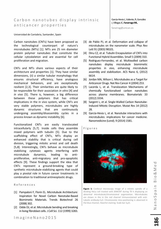
I m a g i n e N a n o 2 0 1 5
Na
no
Sp
ain
Bio
&M
ed
18
6
C a r b o n n a n o t u b e s d i s p l a y i n t r i n s i c a n t i c a n c e r p r o p e r t i e s Universidad de Cantabria, Santander, Spain
Carbon nanotubes (CNTs) have been proposed as the technological counterpart of nature’s microtubules (MTs) [1]. MTs are 25 nm diameter protein polymer nanotubes that constitute the cellular cytoskeleton and are essential for cell proliferation and migration. CNTs and MTs share various aspects of their architecture and properties [1]. They have similar dimensions, (ii) a similar tubular morphology that ensures structural efficiency, have analogous mechanical behaviors, and are exceptionally resilient [2,3]. Their similarities are quite likely to be responsible for their association in vitro [4] and in vivo [5]. There is, however, a big difference between these polymers that has critical implications in the in vivo system, while CNTs are very stable polymers, microtubules are highly dynamic structures that are continuously undergoing assembly/disassembly cycles in a process known as dynamic instability [6]. Functionalized CNTs are easily translocated intracellularly [5,7]. Inside cells they assemble mixed polymers with tubulin [5]. Due to the scaffolding effect of CNTs, MTs display an enhanced stability that is critical during cell division, triggering mitotic arrest and cell death [5,8]. Interestingly, CNTs behave as microtubule stabilizing cytotoxic agents interfering with microtubule dynamics, leading to anti-proliferative, anti-migratory and pro-apoptotic effects [9]. These findings support the idea that CNTs represent a ground-breaking type of synthetic microtubule-stabilizing agents that could play a pivotal role in future cancer treatments in combination to traditional antineoplastic drugs. R e f e r e n c e s
[1] Pampaloni F, Florin EL. Microtubule Architecture:
Inspiration for Novel Carbon Nanotube-Based Biomimetic Materials. Trends Biotechnol 26 (2008) 302.
[2] Odde DJ, et al. Microtubule bending and breaking in living fibroblast cells. J Cell Sci. 112 (1999) 3283.
[3] de Pablo PJ, et al. Deformation and collapse of microtubules on the nanometer scale. Phys Rev Lett 91 (2003) 98101.
[4] Dinu CZ, et al. Tubulin Encapsulation of CNTs into Functional Hybrid Assemblies. Small 5 (2009) 310.
[5] Rodriguez-Fernandez, et al. Multiwalled carbon nanotubes display microtubule biomimetic properties in vivo, enhancing microtubule assembly and stabilization. ACS Nano 6, (2012) 6614.
[6] Jordan MA, Wilson L. Microtubules as a Target for Anticancer Drugs. Nat Rev Cancer 4 (2004) 253.
[7] Lacerda L, et al. Translocation Mechanisms of chemically functionalised carbon nanotubes across plasma membranes. Biomaterials 33 (2012) 3334.
[8] Sargent L, et al. Single-Walled Carbon Nanotube-Induced Mitotic Disruption. Mutat Res 14 (2012) 28.
[9] García-Hevia L, et al. Nanotube interactions with microtubules: implications for cancer medicine. Nanomedicine (Lond). 9 (2014) 1581.
F i g u r e s
Figure 1: Confocal microscopy image of a mitotic spindle of a dividing HeLa cell treated with MWCNT during 70 h displaying an abnormal microtubule/chromosomal organization. Microtubules are shown in the in the red channel immunostained with anti-tubulin antibody-Cy3. Chromosome miss-positioning is observed in the blue channel, Hoechst staining. Scale bar 2μm.
García-Hevia L, Valiente, R, González J, Villegas JC, Fanarraga ML.

I m a g i n e N a n o 2 0 1 5
Na
no
Sp
ain
Bio
&M
ed
18
7
D e s i g n i n g s m a r t v e s i c l e s f o r d r u g d e l i v e r y Adolphe Merkle Institute, University of Fribourg & Chemistry Department, University of Fribourg
Delivering and releasing drugs at their target in a controlled fashion remains a key determinant of successful treatment. Liposomes acting as basic drug carriers are forerunners in this development, and combining them with various stimuli-responsive nanoparticles – which act as release triggers - has become an increasingly popular methodology to control the spatial and temporal release of an encapsulated drug. Developing such hybrids however requires an interdisciplinary bottom-up approach which starts from basic chemical synthesis over precise microscopic characterization to biological settings. In our research group, we apply nanoparticles of different materials (i.e. superparamagnetic iron oxide nanoparticles/SPIONs and gold nanorods/AuNRs) and combine them with thermoresponsive liposomes, either by incorporating them directly in the vesicle bilayer (i.e. via self-assembly) or by functionalizing them to the surface (i.e. via cross-linking). These materials are biocompatible and meticulously tuned to react to a maximum degree to various stimuli (i.e. magnetic and light) - which are presently found in medical
settings - to consequently facilitate the transition from bench to bedside. To optimize our systems, we characterize these nanoscopic hybrids with state-of-the-art cryogenic microscopy techniques to assess their structural and architectural properties under unadulterated conditions. This approach has recently led to the development of Janus magnetic liposomes[1], which were designed by deeply understanding and steering of the liposome self-assembly process. With this research, we hope to contribute to the development of next-generation drug carriers by providing effective, well-characterized and reliable materials to treat conditions such as cancer and inflammatory diseases. R e f e r e n c e s
[1] Bonnaud, C.*, Monnier, C. A.*, Demurtas, D., Jud, C., Vanhecke, D., Montet, X., . & Petri-Fink, A. (2014). Insertion of Nanoparticle Clusters into Vesicle Bilayers. ACS Nano, 8(4), 3451-3460.
F i g u r e s
Alke Fink,
I m a g i n e N a n o 2 0 1 5
Na
no
Sp
ain
Bio
&M
ed
18
8
C o r r e l a t i v e a t o m i c f o r c e a n d s u p e r -r e s o l u t i o n f l u o r e s c e n c e m i c r o s c o p y : a n o v e l t o o l f o r c h a r a c t e r i z a t i o n a t t h e n a n o s c a l e IMDEA Nanociencia, C/ Faraday 9, Ciudad Universitaria de Cantoblanco, Madrid 28049, Spain
Fluorescence microscopy is an essential tool in many fields of science, particularly in biological and biomedical research. However, its spatial resolution is limited by light diffraction to about 200 nm, which precludes its application to the study of subcellular structures and its wide implementation in nanoscience. Currently, approaches for improving the spatial resolution in fluorescence microscopy are experiencing a spectacular expansion and recognition, including the recent award of the Nobel Prize in Chemistry 2014. Several imaging schemes have been successful in breaking the diffraction limit and achieving a spatial resolution of tens of nm [1]. One alternative for super-resolution imaging is photoactivated-localization microscopy (PALM), also termed stochastic optical reconstruction microscopy (STORM). PALM, STORM and related techniques rely on the combination of photoswitchable fluorescent labels, a wide-field fluorescence microscope with single-molecule sensitivity, and image post-processing. These techniques are in continuous development, and new fluorescence labelling and image analysis methods need to be tested. Both labelling and postprocessing analysis are prone to imaging artifacts, therefore new tools that allow robust validation o super-resolution images are needed. For that purpose, we have implemented a novel correlative microscope that allows sequential in situ imaging of the same sample area by atomic force microscopy (AFM) and PALM/STORM [2]. The technical aspects of the correlative microscope, including image alignment and sample preparation requirements will be discussed, as well as its application in optimizing DNA super-resolution imaging. The combination of super-resolution and AFM is not only a useful tool to improve current nanoscopy methods but also to answer new biological questions.
R e f e r e n c e s
[1] S. W. Hell, Nat. Methods, 6 (2009) 24. [2] A. Monserrate, S. Casado, C. Flors,
ChemPhysChem, 15 (2014) 647.
Aitor Monserrate, Santiago Casado, Cristina Flors

I m a g i n e N a n o 2 0 1 5
Na
no
Sp
ain
Bio
&M
ed
18
9
U s i n g p e p t i d e s t o s t u d y a n d m o d u l a t e p r o t e i n i n t e r a c t i o n s f o r t h e r a p e u t i c p u r p o s e s Institute of Chemistry, the Hebrew University of Jerusalem, Givat Ram, Jerusalem, Israel
Our group is interested in using peptides for the quantitative biophysical and structural analysis of protein-protein interactions (PPI) in health and disease. Based on this, we develop lead compounds that modulate PPI for therapeutic purposes. Peptides serve as major tools both for studying PPI and for modulating them (by inhibition or activation). In my talk I will present an overview of our research, focusing on the following examples:
1. Using peptides to modulate the oligomeric state of proteins [1,2]. Many disease-related proteins are in equilibrium between active and inactive oligomeric states. Specific binding of peptides to one of the oligomeric states of such protein should result in stabilization of this state and consequently in shift of the oligomerization equilibrium towards it. We term peptides with such activity as “shiftides”, and they can be utilized therapeutically in two manners: (i) inhibiting a protein by shiftides that bind preferentially to its inactive oligomeric state and stabilize it; (ii) activating a protein by shiftides that bind preferentially to the active oligomeric state and stabilize it. Examples for shiftides developed in o ur lab will be described for the HIV-1 integrase [2,3].
2. Development of new synthetic methods for peptide modifications. We developed a new approach for peptide cyclization during solid phase synthesis under highly acidic conditions [4]. Our approach involves simultaneous in situ deprotection, cyclization and TFA cleavage of the peptide, which is achieved by forming an amide bond between a lysine side chain and a succinic acid linker at the peptide N-terminus. The reaction proceeds via a highly active succini mide intermediate, which was isolated and characterized. Our new methodology is applicable for the formation of macrocycles in solid phase synthesis of peptides and organic molecules. We also developed a new general N-acetylation method for solid phase synthesis [5]. Malonic acid is used as precursor and the reaction proceeds by
in situ formation of a reactive ketene intermediate at room temperature.
3. Intrinsically disordered proteins as drug targets: About one third of the genome encodes for intrinsically disordered proteins (IDPs) or disordered regions in proteins (IDRs). These lack stable tertiary structures and are composed of a large ensemble of extended and flexible conformations interchanging dynamically. IDPs are involved in many human diseases, making them attractive targets for drug design. However, more than 90% of current drug targets are enzymes or receptors and IDPs still cannot be targeted due to the lack of specific binding pockets for small molecules. Our research focuses on how intrinsic protein disorder regulates protein activity with the ultimate goal of setting IDPs and IDRs as therapeutic targets. In my talk I will describe our studies regarding several IDRs including: (1) the pro-apoptotic ASPP2 protein [6,7]; (2) The HIV - 1 Rev protein [8]; (3) the centrosomal STIL protein, which is upregulated in cancer [9].
R e f e r e n c e s
[1] Gabizon, R. and Friedler A. (2014) Front
Chem.;2:9 [2] Hayouka, Z., et al., (2007) Proc Natl Acad Sci U
S A,. 104(20): p. 8316-21. [3] Hayouka, Z., et al., (2010) Bioorg Med Chem,.
18(23): p. 8388-95. [4] Chandra K, et al.(2014; Angew Chem Int Ed
Eng, 53(36):9450-5 [5] Chandra K, et al. (2014) Org Biomol Chem.
12(12):1879-84 [6] Rotem, S. et al. (2008) J Biol Chem 283, 18990-
1899, [7] Rotem-Bamberger, S. et al. (2013) PLoS One
8,e58470, [8] Faust, O. et al. (2014) Chem Comm
50(74):10797-800 [9] Amartely, H. et al. (2014) Chem Comm,
50(40):5245-7.
Assaf Friedler

I m a g i n e N a n o 2 0 1 5
Na
no
Sp
ain
Bio
&M
ed
19
0
N A N O I M P L A N T : n a n o s t r u c t u r e d b i o c o m p a t i b l e c o a t i n g s t o p r e v e n t o r t h o p e d i c i m p l a n t i n f e c t i o n s 1 IMM-Instituto de Microelectronica de Madrid (CNM-CSIC), Isaac Newton 8, 28760 Tres Cantos, Madrid, Spain 2 Dpto. Quimica Inorganica y Bioinorganica. Universidad Complutense de Madrid. Instituto de Investigacion Sanitaria Hospital 12 de Octubre i+12, 28040 Madrid, Spain 3 CIBER de Bioingenieria, Biomateriales y Nanomedicina (CIBER-BBN), Spain 4 Instituto de Ciencia de Materiales de Sevilla (CSIC-US), Seville,Spain 5 Department of Clinical Microbiology. IIS-Fundacion Jimenez Diaz, UAM, Spain
Bacterial colonization and biofilm formation on orthopedic implants is one of the worst possible scenarios in orthopedic surgery, in terms of both patient prognosis and healthcare costs [1]. Tailoring the surface of these orthopedic implants to actively promote bone bonding, while avoiding bacterial colonization, represents an interesting challenge to reach better clinical outcomes [2]. Currently, it has been demonstrated a strong dependence of structural features in the nano-scale with antibacterial effects. Several naturally existing surfaces such as plant leaves and insect wings are capable of maintaining a contaminant-free status despite the innate abundance of contaminants in their surrounding environments [3]. These properties are related to the presence of a periodic topography of hexagonal arrays of nanopillar on their surfaces. By mimicking the nature, and to translate this effect to orthopedic metallic biomaterials, a Ti6Al4V alloy of medical grade has been coated with Ti nanostructures employing the glancing angle deposition technique by magnetron sputtering. The resulting surfaces have a high density of nanocolumnar structures based on Ti, providing high roughness and a notable decrease of wettability. These nanostructured coatings exhibit a selective behavior towards osteoblast and bacteria proliferation. While these nanotextured surfaces strongly impair bacteria adhesion and inhibit biofilm formation, the osteoblasts exhibit almost identical behavior than that obtained onto the initial Ti6Al4V substrates. This selective behavior is discussed on the basis of a “lotus leaf effect” induced by the nanostructured surface and the different size of osteoblasts and bacteria. The obtained results provide new perspectives for manufacturing Ti6Al4V-based implants to prevent infections. Moreover, it is also worth noticing that our work has won the 2014 IDEA² Madrid Award of
the Madrid-MIT M+Vision Consortium, a partnership of the regional government of Madrid and the Massachusetts Institute of Technology (MIT), which fosters innovation in biotechnology [4].
R e f e r e n c e s
[1] Arcos D, Boccaccini AR, Bohner M, Diez-Perez A,
Epple M, et al. Opinion paper. Acta Biomater(2014), http://dx.doi.org/10.1016/j.actbio.2014.01.004
[2] Campoccia D, Montanaro L, Arciola CR. Biomaterials 34 (2013) 8533.
[3] E.P. Ivanova, J. Hasan, H.K. Webb , V. K. Truong, et al. Small 8 (2012) 2489.
[4] http://mvisionconsortium.mit.edu/idea2
J.M. Garcia-Martin1,
I. Izquierdo-Barba2,3, D. Arcos2,3, R. Alvarez4, A. Palmero4, J. Esteban5, C. Perez-Jorge5, M. Vallet-Regi2,3
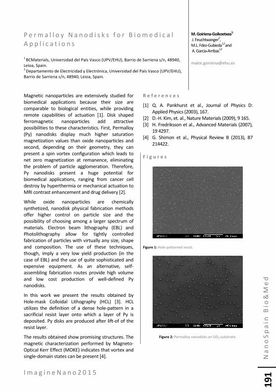
I m a g i n e N a n o 2 0 1 5
Na
no
Sp
ain
Bio
&M
ed
19
1
P e r m a l l o y N a n o d i s k s f o r B i o m e d i c a l A p p l i c a t i o n s 1 BCMaterials, Universidad del País Vasco (UPV/EHU), Barrio de Sarriena s/n, 48940, Leioa, Spain. 2 Departamento de Electricidad y Electrónica, Universidad del País Vasco (UPV/EHU), Barrio de Sarriena s/n, 48940, Leioa, Spain.
Magnetic nanoparticles are extensively studied for biomedical applications because their size are comparable to biological entities, while providing remote capabilities of actuation [1]. Disk shaped ferromagnetic nanoparticles add attractive possibilities to these characteristics. First, Permalloy (Py) nanodisks display much higher saturation magnetization values than oxide nanoparticles and second, depending on their geometry, they can present a spin vortex configuration which leads to net zero magnetization at remanence, eliminating the problem of particle agglomeration. Therefore, Py nanodisks present a huge potential for biomedical applications, ranging from cancer cell destroy by hyperthermia or mechanical actuation to MRI contrast enhancement and drug delivery [2].
While oxide nanoparticles are chemically synthetized, nanodisk physical fabrication methods offer higher control on particle size and the possibility of choosing among a larger spectrum of materials. Electron beam lithography (EBL) and Photolithography allow for tightly controlled fabrication of particles with virtually any size, shape and composition. The use of these techniques, though, imply a very low yield production (in the case of EBL) and the use of quite sophisticated and expensive equipment. As an alternative, self-assembling fabrication routes provide high volume and low cost production of well-defined Py nanodisks.
In this work we present the results obtained by Hole-mask Colloidal Lithography (HCL) [3]. HCL utilizes the definition of a dense hole-pattern in a sacrificial resist layer onto which a layer of Py is deposited. Py disks are produced after lift-of of the resist layer.
The results obtained show promising structures. The magnetic characterization performed by Magneto-Optical Kerr Effect (MOKE) indicates that vortex and single-domain states can be present [4].
R e f e r e n c e s
[1] Q. A. Pankhurst et al., Journal of Physics D: Applied Physics (2003), 167.
[2] D.-H. Kim, et. al., Nature Materials (2009), 9 165. [3] H. Fredriksson et al., Advanced Materials (2007),
19 4297. [4] G. Shimon et al., Physical Review B (2013), 87
214422. F i g u r e s
Figure 1: Hole-patterned resist.
Figure 2: Permalloy nanodisks on SiO2 substrate.
M. Goiriena-Goikoetxea1,
J. Feuchtwanger2, M.L. Fdez-Gubieda1,2 and A. García-Arribas1,2

I m a g i n e N a n o 2 0 1 5
Na
no
Sp
ain
Bio
&M
ed
19
2
A p p l i c a t i o n o f P h o t o c a t a l y t i c a l A c t i v i t y o f C d S N a n o p a r t i c l e s t o D e v e l o p m e n t o f S e n s i t i v e C o l o r i m e t r i c E n z y m a t i c A s s a y s U s i n g 3 , 3 , 5 , 5 ’ - t e t r a m e t h y l b e n z i d i n e ( T M B ) a s a U n i v e r s a l C h r o m o g e n i c C o m p o u n d Biofunctional Nanomaterials, CIC biomaGUNE, Parque Tecnológico de San Sebastian, Paseo Miramon 182, 20009 Donostia- San Sebastian, Spain
Metallic and semiconductor nanoparticles (NPs) can be very conveniently employed for signal transduction and signal amplification by physical methods. Their chemical and physical properties are defined by three dimensional structure of NPs, therefore very slight changes in shape and size lead to drastic variation in absorption and emission spectra. Semiconductor NPs can be photo-excited producing electron/hole couples, which recombine to yield emission of light. Quantum effects in inorganic NPs give rise to fluorescence, therefore such fluorescent particles are referred to in the literature as quantum dots (QDs) [1].
Our laboratory has introduced application of in situ growth of QDs to development of flourogenic enzymatic assays [2]. This concept is based on registration of fluorescence originating from CdS QDs influenced by products of an enzymatic reaction. Those fluorogenic assays showed low detection limits and high signal to noise ratio, but unfortunately the read-out signal was not stable with time. The size of semiconductor QDs defines quantum effects governing fluorescence emission. It was found out that semiconductor CdS nanoparticles (NPs) are able to catalyze photo-oxidation of the well known chromogenic enzymatic substrate 3,3’,5,5’-tetramethylbenzidine (TMB), traditionally employed in quantification of peroxidase activity in the presence of hydrogen peroxide. The photocatalytical oxidation of TMB by oxygen does not require hydrogen peroxide and its rate is directly proportional to the quantity of CdS NPs produced in situ through the interaction of Cd2+ and S2- ions in an aqueous medium. The present concept permits to extend utility of the enzymatic substrate TMB, traditionally employed for detection of horseradish peroxidase activity, to other enzymes participating in formation of semiconductor NPs. In other words, the new approach allows to employ
inexpensive commercially available TMB as a universal chromogenic substrate for quantification of different classes of enzymes.
This phenomenon was applied to development of colorimetric sensitive assays for glucose oxidase and glutathione reductase based on enzymatic generation of CdS NPs acting as light-powered catalysts as demonstrated in Figure 1. Sensitivity of the developed chromogenic assays was of the same order of magnitude or even better than that of relevant fluorogenic assays. The present approach opens the possibility for the design of simple and sensitive colorimetric assays for a number of enzymes using inexpensive and available TMB as a universal chromogenic compound.
R e f e r e n c e s
[1] Parak, W. J.; Manna, L.; Simmel, F. C.; Gerion, D.; Alivisatos, P. In Nanoparticles; Wiley-VCH Verlag GmbH & Co. KGaA, (2005) 4-49
[2] Malashikhina, N.; Garai-Ibabe, G.; Pavlov, V. Anal Chem, 85 (2013) 6866-6870.
F i g u r e s
Figure 1: Chromogenic detection of enzyme activity using photocatalytical oxidation of TMB enhanced by enzymaticaly produced CdS NPs.
Ruta Grinyte, Gaizka Garai-Ibabe, Laura Saa, Valery Pavlov

I m a g i n e N a n o 2 0 1 5
Na
no
Sp
ain
Bio
&M
ed
19
3
D e c o l o r i z a t i o n f o r I n d u s t r i a l W a s t e w a t e r T r e a t m e n t w i t h I m m o b i l i z a t i o n o f L a c c a s e t o t h e N a n o c o m p o s i t e M a t r i x 1 Faculty of Agricultural Sciences and Technologies, Nigde University, Nigde, Turkey 2 Institute of Graduate in Science & Engineering, Division of Nanotechnology and Nanomedicine, Hacettepe University, Beytepe, Ankara, Turkey Abstract -In this study, laccase enzyme (E.C.1.10.3.2.) that produced Trametes versicolor was immobilized through physical adsorption to the nanocomposite structure which used for decolorization of reactive coloring substance (Reactive Red 5) in the industrial originated wastewaters. Optimum physiological conditions such as optimum pH, temperature, the initial colored substance concentration, time-dependent decolorization rate were determinated for the laccase immobilization and these datas were applied and compared both free and immobilized laccase for effective decolorization of industrial wastewater at lab scale.
Keywords: Nanocomposites, enzyme immobilization, laccase, removing of azo dyes.
Introduction-Using of microorganismal originated enzymes for decolorization of industrial waste water offers considerable advantages. This nanobiotechnological process is cheap and economic, also the last products that obtained during mineralization are not toxic [1, 2]. Even though physico-chemical methods are effective in dye removal, some problems such as the overall cost, regeneration, secondary pollutants, limited versatility, interactions with other wastewater constituents and residual sludge generation limit their usage [3]. As an alternative, biological treatments are a relatively inexpensive way to remove dyes from wastewater [4]. In this work, fungal originated laccase enzymes were studied with a nanotechnological way for this kind of removal process.
Experimental-Laccase immobilization to the synthesized poly(maleic anhydride-alt-methyl vinyl ether)/octadecylamine-montmorillonite nanostructures were examined under the optimum conditions (pH, temperature, laccase initial concentration and time). After then, for effectively decolorization process, the optimum conditions (pH, temperature, the initial coloring substance concentration, time-dependent
decolorization rate) were determined for both free and immobilized laccase enzymes.
Results and Discussion-The optimum conditions for the fungal originated laccase immobilization to the poly(maleic anhydride-alt-methyl vinyl ether)/octadecylamine-montmorillonite nanocomposites were determined as 4.5 pH, 37oC temperature, 0.025 mg/ml laccase initial concentration, and 60 minutes at the first stage of the study. After then, for effectively decolorization, the optimum pH was stated as 5.0 and temperature was also stated as 20 0C for both free and immobilized laccase. Moreover, the initial coloring substance concentration was 0,025 mg/L and 0,05 mg/L for free and immobilized laccase, respectively. In our research was determinated as optimum time 120 min.(63% decolorization rate) and 90 min. (70% decolorization rate) for free enzyme and immobilized laccase respectively. At the end of 27 days, while immobilized laccase activity was 65%, free enzyme activity was 33%. Lastly, laccase productivity was found as 77.3% for reusing in effectively decolorization at 10 times over in a period of three days.
R e f e r e n c e s
[1] Duran N., Rosa M.A., D’annibale A., Gianfreda L.. Applications of laccases and tyrosinases (phenoloxidases) immobilized on different supports: a review, Enzyme Microbiol. Technol. 2002; 31, 907–931.
[2] Esther Forgacsa, Tibor Cserhati, Gyula Oros, Removal of synthetic dyes from wastewaters: a review, Environment international, 2004; 30, 953–971.
[3] Mohan S.V., Rao N.C., Sarma P.N., Simulated acid azo dye (Acid black 210) wastewater treatment by periodic discontinuous batch mode operation under anoxic-aerobic-anoxic microenvironment conditions, Ecol. Eng., 2007; 31, 242-250.
[4] Davies L.C., Carias C.C., Novais J.M., Martins-Dias S., Phytoremediation of textile effluents containing azo dye by using Phragmites australis in a vertical flow intermittent feeding constructed wetland, Ecol. Eng., 2005; 25, 594-605.
Sedef Ilk1, Necdet Sağlam2, Zakir
M.O. Rzayev2

I m a g i n e N a n o 2 0 1 5
Na
no
Sp
ain
Bio
&M
ed
19
4
C h i t o s a n N a n o p a r t i c l e s f o r s i R N A B a s e d G e n e S i l e n c i n g T h e r a p y f o r C a n c e r 1 Nanotechnology and Nanomedicine Division, Hacettepe University, Beytepe, 06800, Ankara, Turkey 2 Chemistry Department, Biochemistry Division, Hacettepe University, Beytepe, 06800, Ankara, Turkey 3 Bioengineering Department, Kırıkkale University, Yahşihan, 71451, Kırıkkale, Turkey
Small interfering RNA (siRNA) based gene silencing that reduces the synthesis of specific harmful protein at mRNA level is one of the effective targeted therapies for cancer [1,2]. However, siRNA delivery into the cells is limited due to its rapid decomposition by nucleases and poor cellular uptake [3]. The polycationic, non-toxic, biodegradable and biocompatible polymer such as chitosan (CS) can be bound effectively to siRNA molecule and it can be protected against to enzymatic degradation [4]. In this study CS nanoparticles (NPs) were produced via ionic gelation method and sodium tripolyphosphate (TPP) was used as crosslinker. pH value of the CS solution (4.0 to 5.0) and CS/TPP mass ratio (2.5:1 to 5:1) were changed to optimize the NPs size and surface charge for efficient gene transfection. Morphological characterization of the CS-NPs was evaluated by AFM and SEM. The genes for ABCE1 (ATP-binding casette E1) and eRF3 (eukaryotic release factor 3) proteins which play significant roles in protein synthesis were chosen as target genes to be loaded with CS-NPs, individually and together. Loading efficiencies of 98.69%±0.051 and 98.83%±0.047 were achieved when ABCE1 siRNA and eRF3 siRNA were entrapped into the NPs, respectively. Cellular uptake of fluorescein labeled CS-NPs into MCF-7 cells, WST-1 cytotoxicity and Real Time Cell Analyzer (RTCA) assays of the NPs were carried out. Mean diameter of the CS-NPs was obtained between 105-230 nm and the zeta potential was 27 mV at pH 4.5 and 3:1 CS/TPP mass ratio values. Fig. 1 shows that CS-NPs are spherical in shape by SEM analysis. Both WST- 1 and RTCA assays revealed that ABCE1 siRNA, eRF3 siRNA and ABCE1/eRF3 siRNA loaded NPs significantly reduced the cell viabilty and proliferation (Figure 2). This work demonstrated that the CS-NPs suitable in size and surface charge are promising vectors for siRNA based targeted cancer therapy.
R e f e r e n c e s
[1] Ozpolat B, Sood AK, Lopez-Berestein G,
Advanced Drug Delivery Reviews, 66 (2014) 110-116.
[2] Oh YK, Park TG, Advanced Drug Delivery Reviews, 61 (2009) 850-862.
[3] Piao L, Li H, Teng L, Yung BC, Sugimoto Y, Brueggemeier RW, Lee RJ, Nanomedicine-Nanotechnology, Biology and Medicine, 9 (2013) 122-129.
[4] Ravi Kumar MNV, Reactive Functional Polymers 46 (2000) 1-27.
F i g u r e s
Figure 1: SEM micrographs of CS-NPs.
Figure 2: Cell proliferation curve of MCF-7 cells treated with control and siRNA loaded CS-NPs
Burcu Bağdat Cengiz1, Mehmet Doğan Aşık 1, Göknur Kara
2, Mustafa Türk 3,
Emir Baki Denkbaş 2
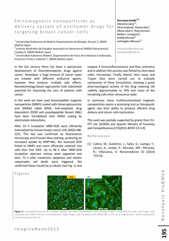
I m a g i n e N a n o 2 0 1 5
Na
no
Sp
ain
Bio
&M
ed
19
5
F e r r o m a g n e t i c n a n o p a r t i c l e s a s d e l i v e r y s y s t e m o f a n t i t u m o r d r u g s f o r t a r g e t i n g b r e a s t c a n c e r c e l l s 1 Universidad Autónoma de Madrid, Departamento de Biología, Darwin 2, 28049 Madrid, Spain. 2 Instituto Madrileño de Estudios Avanzados en Nanociencia (IMDEA Nanociencia), Faraday 9, 28049 Madrid, Spain. 3 Universidad Autónoma Madrid, Departamento de Física de la Materia Condensada, Francisco Tomás y Valiente 7, 28049 Madrid, Spain.
In the last century there has been a spectacular development of chemotherapeutic drugs against cancer. Nowadays a huge amount of cancer types are treated with different antitumor agents, however they produce multiple side effects. Nanotechnology-based approaches hold substantial potential for improving the care of patients with cancer.
In this work we have used biocompatible magnetic nanoparticles (MNPs) coated with dimercaptosuccinic acid (DMSA) called MF66. Anti-neoplastic drug doxorubicin (DOX) and pseudopeptide Nucant (N6L) have been immobilized onto DMSA coating by electrostatic interactions.
After 24 h incubation MNP-DOX were efficiently internalized by human breast cancer cells (MDA-MB-231). This fact was confirmed by fluorescence microscopy and Prussian blue staining, producing an increased uptake by MNP-N6L. We assessed DOX linked to MNPs was more efficiently retained into cells than free DOX. Up to 48 h after MNP-DOX incubation aberrant mitosis were appeared and later, 72 h after treatment, apoptosis and mitotic catastrophe cell death were triggered. We confirmed these results by α-tubulin (see Fig. 1) and
caspase 3 immunofluorescence and flow cytometry and in addition this process was filmed by time-lapse video microscopy. Finally Alamar blue assay and Trypan blue were carried out to evaluate cytotoxicity of these formulation, showing a great pharmacological activity of the drug reducing cell viability approximately to 50% and many of the remaining cells enter senescence state.
In summary, these multifunctionalized magnetic nanoparticles seems a promising tool as therapeutic agent, due their ability to produce efficient drug delivery and cancer cells inactivation.
This work was partially supported by grants from EU-FP7 (no 262943) and Spanish Ministry of Economy and Competitiveness (CTQ2013-48767-C3-3-R)
R e f e r e n c e s
[1] Calero, M.; Gutiérrez, L.; Salas, G.; Luengo, Y.; Lázaro, A.; Acedo, P.; Morales, MP.; Miranda, R.; Villanueva, A. Nanomedicine 10 [2014] 733-43.
F i g u r e s
Figure 1: Immunofluorescence for α-tubulin (green) and DNA counterstained with Hoechst-33258 in MDA-MB-231 cells. Left image: cells incubated with MF66 without functionalization. Right image: cells incubated with MF66-DOX at the same magnification, where doxorubicin induced increased cell size.
Ana Lazaro-Carrillo*1,2,
Macarena Calero1,2, Pierre Couleaud2, Antonio Aires2, Alfonso Latorre2, Álvaro Somoza2, Aitziber L. Cortajarena2, Rodolfo Miranda2,3
and Angeles Villanueva1,2

I m a g i n e N a n o 2 0 1 5
Na
no
Sp
ain
Bio
&M
ed
19
6
N a n o p h o t o n i c l a b - o n - c h i p b i o s e n s o r s f o r t h e n e x t d i a g n o s t i c s g e n e r a t i o n Nanobiosensors and Bioanalytical Applications Group, Institut Català de Nanociència i Nanotecnologia (ICN2) CSIC and CIBER-BBN, Barcelona, Spain
Modern healthcare is demanding novel diagnostic tools that could enable quick, accurate, reliable, and cost-effective results so that appropriate treatments can be implemented in time, leading to improved clinical outcome. Such hand-held point-of-care (POC) devices, able to deliver an instant diagnostics of our health status at home, at doctor's office, at bed side or at resource-limited settings, could become a reality soon thanks to the last advances in nanobiosensors, lab-on-a-chip, wireless and smart-phone technologies which promise to surpass the existing challenges, opening the door to a global health access. Remarkable progress towards POC systems appears continuously in the scientific literature as for example POC technologies coupled to smart-phones, Google glass or paper-based biosensors. However there is still a lack of commercial POC devices as general diagnostic tools due to the many technical challenges to be overcome. The driving force of our research is to achieve such ultrasensitive platforms for POC label-free analysis accomplishing the requirements of disposability and portability. We are using an innovative design
of a nanophotonic biosensor fabricated with silicon photonics technology (an heteromodal nanointerferometer). Full lab-on-chip integration is pursued by incorporating grating couplers for light coupling, independent microfluidics for each sensing channel, photodetectors for the read-out nd signal processing. Advantages as miniaturization, sensitivities clinically relevant, robustness, reliability, potential for multiplexing and mass production at low cost can be offered by our nanodevices. We have demonstrated the suitability of our lab-on-chip photonic biosensor for the clinical diagnostics with extremely sensitivity, directly using untreated human samples, as for the evaluation of hormones related to endocrine disorders and tumours (below 0.1 pg/ml), the detection of infectious microorganisms (at few cfu/ml) or the detection of microRNA biomarkers related to cancer progression, among others.
F i g u r e s
Figure.1: (right) wafer containing nanophotonic biosensors. (left) LOC device containing 16 nanophotonic waveguide sensors integrated with a polymer microfluidics network.
Laura M. Lechuga

I m a g i n e N a n o 2 0 1 5
Na
no
Sp
ain
Bio
&M
ed
19
7
I n f l u e n c e o f c h e m i c a l c o m p o s i t i o n o n t h e d i s s o l u t i o n o f A Y F 4 : Y b , T m ( A = N a , K o r L i ) u p c o n v e r t i n g n a n o p a r t i c l e s i n w a t e r 1 Jožef Stefan Institute, Jamova 39, 1000 Ljubljana, Slovenia 2 Jožef Stefan International Postgraduate School, Jamova 39, 1000 Ljubljana, Slovenia
Lanthanide-doped fluoride nanoparticles, which exhibit upconversion (UC) fluorescence have a great potential for biomaging and also as components in nanotheranostics.The UC process is characterized by the emission of light with shorter wavelength than that of the excitation source. Of particular interest for bioimaging is the UC at near infrared (NIR) wavelengths, so-called NIR to-NIR UC, which is characteristic for the NPs co-doped with Yb3+ and Tm3+ [1]. Ternary fluorides, like for example NaYF4, were proven to be one of the most suitable host matrices, which allow for efficient NIR-to-NIR UC. Despite the known chemical stability of bulk fluorides (i.e., low solubility in water) [2] our preliminary study [3] revealed that NaYF4:Yb3+,Tm3+ NPs can partly dissolve in water. This is not encouraging for biomedical applications, since lanthanide and flouride ions are cytotoxic in sufficiently large concentrations [4-6]. The aim of this work was to study the effect of chemical composition of ternary alkali fluoride NPs (AYF4, where A = Li, Na or K) on the dissolution degree. The AYF4 NPs co-doped with Yb3+ and Tm3+ (Ln-NPs) were synthesized solvothermally at 200 °C. The synthesis time was adjusted in such a way that the Ln-NPs sizes were several tenths of nanometers. This was inspected with transmission electron microscopy while their crystal structures were analyzed with X-ray powder diffraction. The NIR UC emission of the Ln-NPs around 800 nm was much more intense than the blue emission at 450-470 nm. Aqueous suspensions with 1 mg/ml of Ln-NPs were aged from 1h and up to 3 days at room temperature and at pH~7.4 (similar to that of blood). The solutions, which were obtained after ultrafiltration of the Ln-NPs, were analyzed for the dissolved F− and cations using a combined fluoride ion selective electrode and optical emission spectroscopy, respectively. Partial dissolution of all
the studied Ln-NPs was confirmed and will be discussed in terms of their composition.
R e f e r e n c e s
[1] F. Wang, X. Liu, Chem. Soc. Rev., 38 (2009) 976 [2] H. Itoh, H. Hachiya, M. Tsuchiya, Y. Suzuki, Y.
Asano, Bull. Chem. Soc. Jpn., 57 (1984) 1689 [3] O. Plohl, D. Lisjak, M. Ponikvar-Svet, S. Kralj, D.
Makovec, Proc. of the 6th Jožef Stefan International Postgraduate School Student's Conference – Part 1, Ljubljana, 2015, 255
[4] [4] N. I. Agalakova, G. P. Gusev, ISRN Cell Biol., (2012) 403835
[5] H. Q. Xiao, F. L. Li, Z. Y. Zhang, L. X. Feng, Z. J. Li, J. H. Yang, Z. F. Chai, Toxicol. Lett., 155 (2005) 247
[6] T. Grobner, Dial. Transplant, 21 (2006) 1194
Darja Lisjak1, Olivija Plohl1,2,
Boris Majaron1, Maja Ponikvar-Svet1

I m a g i n e N a n o 2 0 1 5
Na
no
Sp
ain
Bio
&M
ed
19
8
D e s i g n o f m u l t i f u n c t i o n a l l i p o s o m a l d r u g f o r m u l a t i o n s f o r c a n c e r t h e r a p y 1CFUM - Centre of Physics of University of Minho, Campus of Gualtar, Braga, Portugal 2CBMA - Centre of Molecular and Environmental Biology of University of Minho, Campus of Gualtar, 4710-057 Braga, Portugal 3Nanodelivery – I&D em Bionanotechnologia, Lda., Department of Biology, University of Minho, Campus of Gualtar, 4710-057 Braga, Portugal
Cancer remains a global health problem and a major cause of death worldwide. Statistical analysis published by the International Agency for Research on Cancer from the World Health Organization reveals that if the estimated trends continue, the incidence of all cancer cases will raise from 12.7 million new cases in 2008 to 21.2 million by 2030 [1]. Doxorubicin (DOX) is considered one of the main “first-line” anticancer drugs for a broad spectrum of tumor types, but this drug has the disadvantage of being toxic for other healthy organs and tissues. The use of liposomes as carriers of DOX is thus very appealing to counteract this disadvantage and protect the healthy tissues from contact with the DOX toxicity. Despite several liposomal formulations were already proposed for the delivery of DOX, the majority uses “active loading” methods and the small number of liposomal formulations that use “passive loading” methods achieve small encapsulation efficiency (EE) of the drug. The “active loading” methods are used to increase DOX amounts in the nanocarriers, but have however the disadvantage of drug precipitation and formation of dimers for which the therapeutic value is yet to be proved [2]. In this work it is proposed a nanocarrier system of Dioctadecyldimethylammonium Bromide (DODAB) and 1-oleoyl-rac-glycerol (Monoolein (MO)) (1:2) that has previously been studied as a system with great potentiality of encapsulating drugs, not only at the DODAB enriched bilayer level, but also at the inverted non-lamellar MO-enriched phases at the vesicle interior [3]. Therefore with this innovative polymorphic system the lipophylic area is greatly increased thus increasing the system capacity to increase the payload content even by a passive encapsulation. Three methods of DOX passive encapsulation in the formulation DODAB:MO (1:2) were tested and characterized measuring the size and zeta potential of the liposomes overtime by dynamic and electrophoretic light scattering and measuring DOX EE (evaluated through UV/Vis spectrophotometry). EE studies revealed high encapsulation values of
DOX (87 %) turning the developed formulation in a very promising nanocarrier system for DOX. The study of the partition coefficient of DOX has confirmed that it is highly distributed in the lipid formulation. The biophysical effects of DOX in the formulation indicated an increase in the cooperativity of the phase transition confirming DOX distribution at the membrane level. Furthermore, thermodynamical parameters of DOX partitioning indicated that the drug distribution in the lipid formulation occurred spontaneously. Cytotoxicity assays were also performed in a cancer cell line and it was concluded that the formulation with DOX encapsulated in DODAB:MO (1:2) has a better cytostatic effect than the free drug, confirming the potentiality of the developed formulation to be used in cancer treatment. Finally controlled release assays were carried out in media with different relevant physiological pH values (5 and 7.4) to predict the pharmacokinetic behavior of the drug when loaded in the developed nanocarriers. Currently we are exploiting a distinct virtue of the co-delivery system, which is taking advantage of the positive charge of the nanocarrier to deveop hybrid co-delivery nanocarriers that combine chemotherapeutic agents with small interfering ribonucleic acids (siRNA targeted to MRP1 mRNA and siRNA targeted to BCL2 mRNA as suppressors of multidrug resistance).
This work was supported by FEDER through POFC – COMPETE and by national funds from FCT through the projects PEst-OE/BIA/UI4050/2014 and PEST-C/FIS/UI607/2013 and PTDC/QUI/69795/2006. Marlene Lucio holds a position of Researcher FCT with the reference IF/00498/2012. .
R e f e r e n c e s
[1] Bray, F.; Jemal, A.; Grey, N.; Ferlay, J.; Forman, D., The Lancet Oncology, 13 (2012), 790-801.
[2] Barenholz, Y., Journal of Control Release, 160 (2012), 117-134.
[3] Neves Silva, J.P.N; Oliveira, A.C.N.; Lúcio, M; Gomes, A.C.; Coutinho, P.J.G.; Real Oliveira, M.E.C.D., Colloids and Surfaces B: Biointerfaces, 121 (2014), 371-379.
Marlene Lúcio1, Eduarda Bárbara1,
Ana Oliveira1,2, Odete Gonçalves1,3, Andreia C. Gomes2 and M.E.C.D. Real Oliveira1,2

I m a g i n e N a n o 2 0 1 5
Na
no
Sp
ain
Bio
&M
ed
19
9
D i s s e c t i n g t h e M o l e c u l a r M e c h a n i s m o f A p o p t o s i s d u r i n g P h o t o t h e r m a l T h e r a p y u s i n g G o l d N a n o p r i s m s 1 Instituto Universitario de Nanociencia de Aragón, Universidad de Zaragoza, Spain 2Aragón Health Research Institute, Zaragoza, Spain 3CICBiomaGUNE, San Sebastián. Spain 4 Fundacion ARAID, Spain 5 Instituto de Carboquímica, CSIC, Zaragoza, Spain. 6 Faculty of Physics, Philipps-Universität Marburg, Germany 7 Instituto de Ciencia de Materiales de Aragón, CSIC-Universidad de Zaragoza, Spain 8 Shanghai Jiao Tong University, P.R. China
Nature has been utilizing nanostructures for millions of years. The following two properties, (i) being about the size of “typical” biological objects and (ii) the possibility of tailoring their properties by changing their size or their shape, make nanoparticles attractive for biomedical applications. One the most promising application for gold nanoparticles (NPs) is their use as “heaters” during photothermal therapy of solid carcinomas using near-infrared laser light (NIR). The most common cellular response to photothermal therapy treatment (PTT) using this kind of nanomaterials is necrosis, producing detrimental inflammatory responses. Here we report the use of PTT using gold nanoprisms (NPRs)
to specifically induce apoptosis in cells. In order to understand the different molecuar pathways involved in this cellular death, we have analysed the mechanism of apoptosis using embryonic fibrobast cells from different knock out mice, which are deficient in proteins involved in the different routes of apoptosis. Our results show that “hot” NPRs activate the intrinsic/mitochondrial pathway of apoptosis mediated by Bak and Bax through the activation of the BH3-only protein Bid. Finally, apoptosis and cell death is dependent on the presence of both caspase-9 and caspase-3.
Marta Pérez-Hernández1,2, Pablo del Pino,1,3, Scott G. Mitchell1, María Moros1, Grazyna Stepien1, Beatriz Pelaz6, Wolfgang J. Parak6, 3, Eva M. Gálvez5, 2 , Julián Pardo, 1 2,4 and Jesús M. de la Fuente
7, 8

I m a g i n e N a n o 2 0 1 5
Na
no
Sp
ain
Bio
&M
ed
20
0
I n n o v a t i v e B i o s e n s o r s f o r N e w P o i n t - o f - C a r e D e v i c e s 1 CIC microGUNE, Arrasate-Mondragón, Spain 2 Micro-Nanofabrication Unit, IK4-Tekniker, Eibar, Spain
There is a general need in healthcare systems all around the world to reduce costs in terms of time and money without compromising patient outcome. Point-of-Care (POC) testing is currently being used in some applications (e.g. coagulation devices) as an alternative to already established standard central laboratory tests to overcome sample transportation and long turnaround times. The main objective of this investigation is to develop innovative technologies for their integration into POC platforms. In this research, a model protein biomarker was selected as an excuse to prove the potential of the biosensors developed. Tumour Necrosis Factor-alpha (TNF-α) was chosen because it was considered a challenging goal due to its extremely low presence in blood/serum/plasma samples. In addition, assaying of this biomarker is interesting for many immunological studies. For instance, the binding inhibition of circulating TNF-α to its receptors by biological drugs has been seen to alleviate the symptoms of certain diseases such as rheumatoid arthritis or Crohn's disease. With the above-mentioned framework in mind, three different technologies were investigated: Firstly, an electrochemical immunoassay for the detection of proteins in human serum based on the combination of amperometric measurements, magnetic microbeads (MBs) and disposable screen-printed carbon electrodes (SPCEs) has been developed. The specifically modified microbeads were magnetically captured onto the working electrode surface and the electrodic and enzymatic reactions of the H2O2-hydroquinone mediated reduction was amperometrically monitored [1]. Secondly, a novel solid-phase assay based on a magnetic bead-mediated proximity ligation assay (PLA) has been developed in which one of the assay proximity probes was directly immobilized onto streptavidin-coated magnetic beads. The portable device was based on a disposable and single-use cyclo olefin polymer (COP) microfluidic
chip interfaced with a quantitative real-time polymerase chain reaction (qPCR) device [2]. Finally, a simple method for the detection of biomarkers in human serum with great sensitivity has been developed using a surface plasmon resonance (SPR) biosensor. Signal amplification based on a sandwich immunoassay including gold nanoparticles was used. Detection in serum proved to be challenging due to high undesirable non-specific binding to the sensor surface stemming from the matrix nature of the sample [3]. The simplicity, robustness and the clinically interesting LODs obtained with the three methods presented here proved them as good contenders for real clinical application. The knowledge acquired could be horizontally applied to the other interesting protein or DNA biomarkers. The POC platforms envisioned in this project could potentially help in increasing the quality of patient care by reducing turnaround times and improving clinical decision making. It should also be emphasized the possibility of integrating high-throughput, multiplex detection and automatization into the platforms. These advantages may have a significant positive impact on cost in terms of time and money on governmental health service budgets.
R e f e r e n c e s
[1] U. Eletxigerra, J. Martinez-Perdiguero, S. Merino, R. Villalonga, J.M. Pingarrón, S. Campuzano, Anal. Chim. Acta 838 (2014) 37–44.
[2] V. Castro-Lopez, J. Elizalde, M. Pacek, E. Hijona, L. Bujanda, Biosens. Bioelec., 54 (2014) 499-505
[3] J. Martinez-Perdiguero, A. Retolaza, L. Bujanda , S. Merino, Talanta 119 (2014) 492–497
Josu Martínez-Perdiguero1,
Vanessa Castro-López1, Unai Eletxigerra1,2

I m a g i n e N a n o 2 0 1 5
Na
no
Sp
ain
Bio
&M
ed
20
1
S i l i c o n n a n o p a r t i c l e s a s T r o j a n h o r s e s f o r p o t e n t i a l b r e a s t c a n c e r t h e r a p y 1 Centro de Tecnologías Físicas, Unidad Asociada CSIC-UPV, Universidad Politécnica de Valencia, Av. Los Naranjos s/n, Valencia, 46022 Spain 2 Servicio de Oncología, Hospital Universitario Madrid-Torrelodones, Madrid, Spain 3 Departamento de Química Orgánica, Universidade de Vigo, Vigo, 36310 Spain 4 Fachbereich Physik, Philipps Universität Marburg, Marburg, 35037 Germany 5 Medcomtech SA. C/ Catalunya, 83-85 Viladecans, Barcelona, 08840 Spain 6 Departamento de Química Física e Inorgánica, Universitat Rovira i Virgili and Centro de Tecnología Química de Catalunya, Carrer de Marcel•lí Domingo s/n, 43007 Tarragona, Spain 7 ICREA, Passeig Lluís Companys 23, 08010 Barcelona, Spain
Over the last two decades nanoparticles have proven to have a great potential for drug delivery and disease treatment, particularly in cancer therapy strategies [1]. In the last years porous silicon nanoparticles have shown excellent properties as drug delivery carriers for cancer therapy due to their excellent biocompatibility and biodegradability [2]. It is well known from silicon producers that porous silicon nanoparticles present extremely high, and even explosive, oxidation reactions with enthalpy values exceeding that of Trinitrotoluene (TNT) [3]. Here we show that silicon nanoparticles can be used themselves as a cancer cell killer drug [4], thus avoiding the use any additional anticancer drug with serious side-effects. Targeted cells are destroyed through a mechanism that takes advantage of both the violent reaction of degradation of silicon in aqueous medium and the enzymatic machinery of eukaryotic cells. The use of silicon nanoparticle properly protected to avoid an extracellular solubilization, and coupled to an appropriated antibody, allows the selective destruction of the cancer cells, which is followed by the degradation of silicon into excretable biocomponents of the body. Figure 1 shows an example of how the breast cancerous cells (SK-BR3) viability dramatically decreases with porous silicon nanoparticles properly functionalized with the directing vector HER-2 positive breast cancer.
R e f e r e n c e s
[1] Prasad, P.N. Introduction to Nanomedicine and Nanobioengineering. (Wiley, New York; 2012)
[2] Park, J.-H. et al. Nat Mater 8, (2009) 331; Popplewell, J.F. et al. J. Inorg. Biochem. 69 (1998) 177; Shabir, Q. et al. Silicon 3 (2011) 173
[3] Mikulec, et al., Advanced Materials, 14 (2002) 38-41
[4] Fenollosa, R., et al., Journal of Nanobiotechnology 12 (2014) 35
F i g u r e s
Figure 1: Cell viability. Relative cell viability after incubation of SK-BR-3 and MDA-MB-435 cells with PSiPs and PSiPs-HER-2 for 48 h.
Roberto Fenollosa,1 Eduardo Garcia-Rico,2 Susana Alvarez,3 Rosana Alvarez,3 Xiang Yu,4 Isabelle Rodriguez5, Susana Carregal-Romero,4 Carlos Villanueva,5 Pilar Rivera-Gil,5 Angel R. de Lera,3 Wolfgang J. Parak,4 Francisco Meseguer,
1
Ramón A. Alvarez-Puebla,6,7
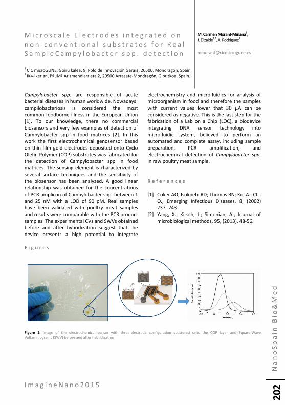
I m a g i n e N a n o 2 0 1 5
Na
no
Sp
ain
Bio
&M
ed
20
2
M i c r o s c a l e E l e c t r o d e s i n t e g r a t e d o n n o n - c o n v e n t i o n a l s u b s t r a t e s f o r R e a l S a m p l e C a m p y l o b a c t e r s p p . d e t e c t i o n 1 CIC microGUNE, Goiru kalea, 9, Polo de Innovación Garaia, 20500, Mondragón, Spain 2 IK4-Ikerlan, Pº JMª Arizmendiarrieta 2, 20500 Arrasate-Mondragón, Gipuzkoa, Spain.
Campylobacter spp. are responsible of acute bacterial diseases in human worldwide. Nowadays campilobacteriosis is considered the most common foodborne illness in the European Union [1]. To our knowledge, there no commercial biosensors and very few examples of detection of Campylobacter spp in food matrices [2]. In this work the first electrochemical genosensor based on thin-film gold electrodes deposited onto Cyclo Olefin Polymer (COP) substrates was fabricated for the detection of Campylobacter spp in food matrices. The sensing element is characterized by several surface techniques and the sensitivity of the biosensor has been analyzed. A good linear relationship was obtained for the concentrations of PCR amplicon of Campylobacter spp. between 1 and 25 nM with a LOD of 90 pM. Real samples have been validated with poultry meat samples and results were comparable with the PCR product samples. The experimental CVs and SWVs obtained before and after hybridization suggest that the device presents a high potential to integrate
electrochemistry and microfluidics for analysis of microorganism in food and therefore the samples with current values lower that 30 μA can be considered as negative. This is the last step for the fabrication of a Lab on a Chip (LOC), a biodevice integrating DNA sensor technology into microfluidic system, believed to perform an automated and complete assay, including sample preparation, PCR amplification, and electrochemical detection of Campylobacter spp. in raw poultry meat sample.
R e f e r e n c e s
[1] Coker AO; Isokpehi RD; Thomas BN; Ko, A.; CL.,
O., Emerging Infectious Diseases, 8, (2002) 237- 243
[2] Yang, X.; Kirsch, J.; Simonian, A., Journal of microbiological methods, 95, (2013), 48-56.
F i g u r e s
Figure 1: Image of the electrochemical sensor with three-electrode configuration sputtered onto the COP layer and Square-Wave Voltammograms (SWV) before and after hybridization
M. Carmen Morant-Miñana1,
J. Elizalde1,2, A. Rodriguez1
I m a g i n e N a n o 2 0 1 5
Na
no
Sp
ain
Bio
&M
ed
20
3
P o l y m e r T h e r a p e u t i c s f o r t h e T r e a t m e n t o f C h r o n i c S p i n a l C o r d I n j u r i e s Centro de Investigación Príncipe Felipe. Eduardo Primo Yúfera 3, 46012 Valencia. 1 Polymer Therapeutics Laboratory. 2 Neuronal and Tissue Regeneration Research group.
The medical application of nanotechnology has enormous potential to improve human health, especially in serious chronic disease such as cancer and neurodegeneration [1-3]. In this sense, Polymer Therapeutics represents an outstanding approach for the treatment of several pathologies, being one of the first nanomedicines with more than 16 polymer-drug conjugates in advanced clinical trials and several already transferred to routine clinical use. Although considerable experimental improvements in neuronal activity in acute and subacute stages after Spinal Cord Injury (SCI) have been made in the last decade, little progress has been made in the chronic stage. In the chronic scenario, tissue degeneration and reactive scarring isolate the injured area from the potential re-growing axons [4]. However, there are currently no studies which cover all fundamental criteria: cell replacement, neuroprotection and axonal growth promotion strategies and even fewer in chronic stages. Considering all tissue degeneration and the massive cell loss that occurs, transplantation of spinal cord derived and functional compatible cells result mandatory for tissue repair. Based on the multifaceted lesion that occurs, a combinatory therapeutic approach is clearly required [5]. We aim to the design of a nanomedicine for neuroprotection and axonal growth promotion. The property of multivalency provided by the use of polymeric carriers allows the conjugation of several bioactive agents in the same polymer in such a way that for SCI, the combination of a neuroprotector with an axonal growth inductor and other active principle such as chondroitinase, for glial scar disruption could markedly enhance the therapeutic value of these macromolecules. In this communication we present a first approach for the combinatorial treatment of SCI, where an axonal growth inductor (Fasudil®) conjugated to a multifunctional and biodegradable polymer such as Poly-L-Glutamic acid (PGA) is evaluated for combination with stem cell transplantation.
The conjugation of Fasudil to PGA has been achieved through different biodegradable linkers (amide and carbamate) and the different release rate profiles and toxicities of the conjugates has been evaluated in vitro showing different release rates depending on the linkage and no associated toxicities. Furthermore, the conjugation of a fluorescent dye (Oregon Green) enabled the study of the cellular uptake on injury activated ependymal cells and points to an energy dependent endocytosis internalization mechanism. In vitro tests on ROCK inhibition activity and axonal elongation has been carried out. All these results are promising for a therapy towards the treatment of SCI based on the combination of polymer conjugates and stem cells transplantation.
R e f e r e n c e s
[1] Ferrari M. Nature Rev. Cancer, 5 (2005), 161. [2] Duncan R. Nat. Rev. Drug. Discov., 2 (2003) ,
347. [3] Fabiana Canal; Joaquin Sanchis; María J. Vicent
22 – 6 (2011), 894. [4] Thuret S., Moon L.D.F., Gage F.H., Nat. Rev. 7
(2006), 628. [5] a) Moreno-Manzano V. et al., 27 (2009), 733.;
b) Moreno-Manzano V. et al. Stem Cells, 30 (2012), 2221.
V. J. Nebot,1 A. Armiñan,1
A. Alastrue-Agudo,2 R. Requejo-Aguilar,2 V. Moreno-Manzano,2 M. J. Vicent.1

I m a g i n e N a n o 2 0 1 5
Na
no
Sp
ain
Bio
&M
ed
20
4
B i o s e n s i n g B a s e d o n E n z y m a t i c M o d u l a t i o n o f G r o w t h o f N a n o p a r t i c l e s CIC BiomaGUNE, Paseo Miramon 182, San Sebastian, Spain
Semiconductor nanoparticles (SNPs) can be very conveniently employed in biosensing for signal transduction. Their chemical and physical properties are defined by three dimensional structure of NPs, therefore very slight changes in shape and size lead to drastic variation in absorption and emissionspectra. We pioneered enzymatic assays in which formation of CdS nanoparticles according to the equation Cd2+ + S2- = CdS is caused by biocatalytic processes yielding S2- ions [1]. The second group of QDs-generating fluorogenic enzymatic assays developed by us relies on modulating the growth of CdS QDs with the products of biocatalytic transformation through inhibition or enhancement. This novel concept has been applied by us to a number of assays, including, the highly sensitive and inexpensive detection of reduced glutathione (GSH), over its oxidized form (GSSG), and glutathione reductase (GR) in human serum [2]. This new fluorogenic bioanalytical system is based on the GR-mediated stabilization of growing CdS nanoparticles (Scheme 1). The sensitivity of this new assay is 5 pM of GR, which is 3 orders of magnitude better than other fluorogenic methods previously reported in the literature. We also managed to show how the growth of fluorescent CdS can be modulated by the DNAzyme having peroxidase activity. The system is based on the affinity interaction between the peroxidase-DNAzyme bearing hairpin sequence and the analyte (DNA or low molecular weight molecule), which changes the folding of the hairpin structure and consequently the activity of peroxidase-DNAzyme [3] (Scheme 2).
Recognition events, such as specific interaction of target analytes with a number of enzymes or affinity interaction in enzyme-linked immunosorbent assays, may lead to formation of fluorescent quantum dots with photocatalytic activity. Our latest experimental results confirm that CdS QDs, grown under the influence of products of biocatalytic transformations, are photo-catalysts enhancing oxidation of commercially available enzymatic chromogenic substrates such as 3,3',5,5'-
tetramethylbenzidine (TMB) and 2,2'-azino-bis(3-ethylbenzothiazoline-6-sulphonic acid) (ABTS). The photocatalysis did not take place under ambient laboratory light but occurred only under irradiation with a standard UV lamp, resulting in high repeatability. We applied this colorimetric method to analytical assays in which the growth of SNPs in situ is modulated by products of enzymatic reactions catalyzed by GOx and GR. The detection limits demonstrated by two developed chromogenic assays were comparable with or better than those of corresponding fluorogenic assays relying on registration of emission light arising from CdS NPs. Due to stability of 3,3’,5’5-tetramethylbenzidine diimine the read-out signal was very stable and standard deviation was quite small [4].
R e f e r e n c e s
[1] V. Pavlov, Part. Part. Syst., 31 (2014) 36. [2] G. Garai-Ibabe, L. Saa, V. Pavlov, Anal. Chem.,
85, (2013) 5542. [3] G. Garai-Ibabe, M. Möller, L. Saa, R. Grinyte, V.
Pavlov, Anal. Chem., 86 (2014) 10059. [4] R. Grinyté, G. Garai, L. Saa, V. Pavlov, Anal.
Chem. In Press.
Valery Pavlov, Ruta Grinyte, Laura Saa, Gaizka Garrai

I m a g i n e N a n o 2 0 1 5
Na
no
Sp
ain
Bio
&M
ed
20
5
F i g u r e s
Scheme 1: Detection of PON1 activity by the enzymatic inhibition of growth of fluorescent CdS QDs.
Scheme 2: DNA detection through peroxidase-DNAzyme modulated growth of CdS QDs in situ.
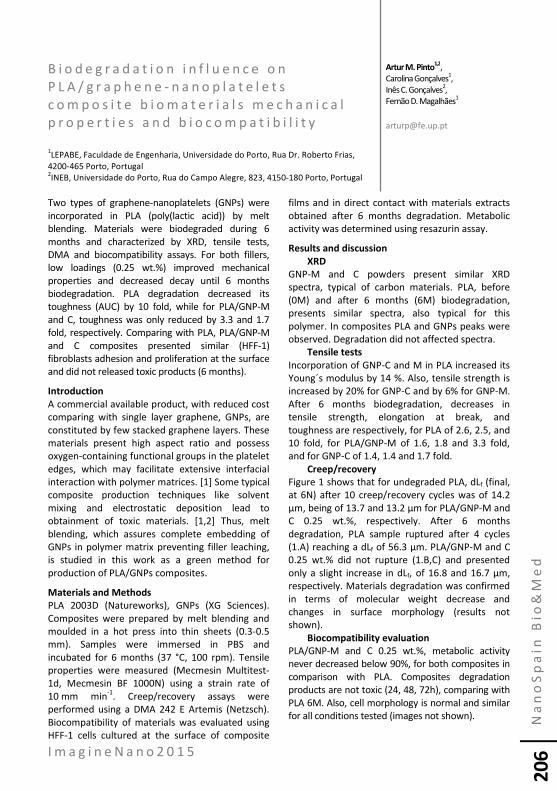
I m a g i n e N a n o 2 0 1 5
Na
no
Sp
ain
Bio
&M
ed
20
6
B i o d e g r a d a t i o n i n f l u e n c e o n P L A / g r a p h e n e - n a n o p l a t e l e t s c o m p o s i t e b i o m a t e r i a l s m e c h a n i c a l p r o p e r t i e s a n d b i o c o m p a t i b i l i t y 1LEPABE, Faculdade de Engenharia, Universidade do Porto, Rua Dr. Roberto Frias, 4200-465 Porto, Portugal 2INEB, Universidade do Porto, Rua do Campo Alegre, 823, 4150-180 Porto, Portugal
Two types of graphene-nanoplatelets (GNPs) were incorporated in PLA (poly(lactic acid)) by melt blending. Materials were biodegraded during 6 months and characterized by XRD, tensile tests, DMA and biocompatibility assays. For both fillers, low loadings (0.25 wt.%) improved mechanical properties and decreased decay until 6 months biodegradation. PLA degradation decreased its toughness (AUC) by 10 fold, while for PLA/GNP-M and C, toughness was only reduced by 3.3 and 1.7 fold, respectively. Comparing with PLA, PLA/GNP-M and C composites presented similar (HFF-1) fibroblasts adhesion and proliferation at the surface and did not released toxic products (6 months).
Introduction
A commercial available product, with reduced cost comparing with single layer graphene, GNPs, are constituted by few stacked graphene layers. These materials present high aspect ratio and possess oxygen-containing functional groups in the platelet edges, which may facilitate extensive interfacial interaction with polymer matrices. [1] Some typical composite production techniques like solvent mixing and electrostatic deposition lead to obtainment of toxic materials. [1,2] Thus, melt blending, which assures complete embedding of GNPs in polymer matrix preventing filler leaching, is studied in this work as a green method for production of PLA/GNPs composites.
Materials and Methods
PLA 2003D (Natureworks), GNPs (XG Sciences). Composites were prepared by melt blending and moulded in a hot press into thin sheets (0.3-0.5 mm). Samples were immersed in PBS and incubated for 6 months (37 °C, 100 rpm). Tensile properties were measured (Mecmesin Multitest-1d, Mecmesin BF 1000N) using a strain rate of 10 mm min-1. Creep/recovery assays were performed using a DMA 242 E Artemis (Netzsch). Biocompatibility of materials was evaluated using HFF-1 cells cultured at the surface of composite
films and in direct contact with materials extracts obtained after 6 months degradation. Metabolic activity was determined using resazurin assay.
Results and discussion
XRD
GNP-M and C powders present similar XRD spectra, typical of carbon materials. PLA, before (0M) and after 6 months (6M) biodegradation, presents similar spectra, also typical for this polymer. In composites PLA and GNPs peaks were observed. Degradation did not affected spectra.
Tensile tests
Incorporation of GNP-C and M in PLA increased its Young´s modulus by 14 %. Also, tensile strength is increased by 20% for GNP-C and by 6% for GNP-M. After 6 months biodegradation, decreases in tensile strength, elongation at break, and toughness are respectively, for PLA of 2.6, 2.5, and 10 fold, for PLA/GNP-M of 1.6, 1.8 and 3.3 fold, and for GNP-C of 1.4, 1.4 and 1.7 fold.
Creep/recovery
Figure 1 shows that for undegraded PLA, dLf (final, at 6N) after 10 creep/recovery cycles was of 14.2 µm, being of 13.7 and 13.2 µm for PLA/GNP-M and C 0.25 wt.%, respectively. After 6 months degradation, PLA sample ruptured after 4 cycles (1.A) reaching a dLf of 56.3 µm. PLA/GNP-M and C 0.25 wt.% did not rupture (1.B,C) and presented only a slight increase in dLf, of 16.8 and 16.7 µm, respectively. Materials degradation was confirmed in terms of molecular weight decrease and changes in surface morphology (results not shown).
Biocompatibility evaluation
PLA/GNP-M and C 0.25 wt.%, metabolic activity never decreased below 90%, for both composites in comparison with PLA. Composites degradation products are not toxic (24, 48, 72h), comparing with PLA 6M. Also, cell morphology is normal and similar for all conditions tested (images not shown).
Artur M. Pinto1,2,
Carolina Gonçalves1, Inês C. Gonçalves2, Fernão D. Magalhães1
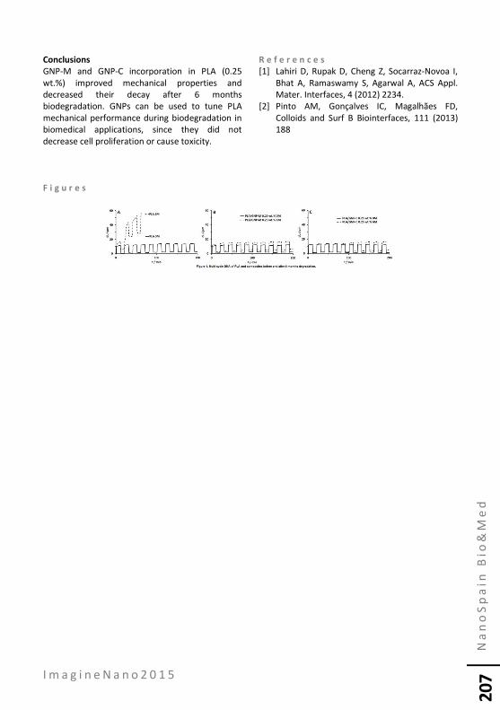
I m a g i n e N a n o 2 0 1 5
Na
no
Sp
ain
Bio
&M
ed
20
7
Conclusions
GNP-M and GNP-C incorporation in PLA (0.25 wt.%) improved mechanical properties and decreased their decay after 6 months biodegradation. GNPs can be used to tune PLA mechanical performance during biodegradation in biomedical applications, since they did not decrease cell proliferation or cause toxicity.
R e f e r e n c e s
[1] Lahiri D, Rupak D, Cheng Z, Socarraz-Novoa I, Bhat A, Ramaswamy S, Agarwal A, ACS Appl. Mater. Interfaces, 4 (2012) 2234.
[2] Pinto AM, Gonçalves IC, Magalhães FD, Colloids and Surf B Biointerfaces, 111 (2013) 188
F i g u r e s

I m a g i n e N a n o 2 0 1 5
Na
no
Sp
ain
Bio
&M
ed
20
8
N a n o s t r u c t u r e d M a t e r i a l s i n M a t r i x -f r e e L a s e r D e s o r p t i o n I o n i s a t i o n M a s s S p e c t r o m e t r y Glycotechnology Laboratory, CIC biomaGUNE, paseo Miramon 182, San Sebastian Spain
Nanostructured surfaces and nanoparticles have contributed enormously to the development of surface based matrix-free soft ionisation techniques like SALDI-MS with important applications in small molecule analysis and imaging mass Spectrometry. This lecture will try to provide brief overview of materials and concepts employed for surface and particle based LDI-MS and discuss in more detail two materials recently developed in the authors laboratory namely, nanostructured indium tin oxide thin films [1] and polished weathering steel [2]. Applications covering imaging mass spectrometry of tissues samples, serum metabolite analysis of quantification of lactose in milk have been chosen to demonstrate the versatility of the materials in a broad range of analytical problems.
R e f e r e n c e s
[1] López, de L. C., Beloqui, A., Yate, L., Calvo, J.,
Puigivila, M., Llop, J., and Reichardt, N. (2015) Nanostructured Indium Tin Oxide Slides for Small-Molecule Profiling and Imaging Mass Spectrometry of Metabolites by Surface-Assisted Laser Desorption Ionization MS. Analytical chemistry 87, 431.
[2] Etxebarria, J., Calvo, J., and Reichardt, N.-C. (2014) Nanostructured weathering steel for matrix-free laser desorption ionisation mass spectrometry and imaging of metabolites, drugs and complex glycans. Analyst 139, 2873–2883
F i g u r e s
Niels-Christian Reichardt

I m a g i n e N a n o 2 0 1 5
Na
no
Sp
ain
Bio
&M
ed
20
9
P r o t e i n s : A M a t e r i a l - S c i e n c e P o i n t o f V i e w Department of Materials Science and Engineering & University Center for Nano Science and Nanotechnology, Tel-Aviv University, Tel-Aviv, Israel
Proteins form the very basis of life. They regulate a variety of activities in all known organisms, from replication of the genetic code to transporting oxygen, and are generally responsible for regulating the cellular machinery and determining the phenotype of an organism. From a material-science point of view, proteins can serve as excellent building blocks for the development of new structures, composites, and devices. In this talk I will describe some of our efforts in this direction. Specifically I will address the followings: (i)Engineered Light-emitting bio-materials, (ii)Control over the electrical properties of nano-sized junctions via “natural” site-controlled doping of proteins monolayers, (iii)Bioinspired photovoltaic cells(iv)
R e f e r e n c e s
[1] Gordiichuk, P. I. et al.. Adv. Mater. 26,
(2014).4863. [2] Mentovich, E. D. et al. J. Phys. Chem. C 117,
(2013) 8468. [3] Mentovich, E., Belgorodsky, B., Gozin, M.,
Richter, S. & Cohen, H. J. Am. Chem. Soc. 134, (2012) 8468.
[4] Hendler, N. et al.. Chem Commun 47, (2011) 7419.
[5] Hendler, N.,et al. Adv. Mater. 23, (2011) 4261. [6] Hendler, N. et al. Macromol. Biosci. 14, (2014)
320. [7] Carmeli, I. et al. Nano Lett. 10, (2010) 2069.
F i g u r e s
Shachar Richter, Netta Hendelr Edith Beilis, Elad Mentovich, Katya Glhih, Antonina Melinchuk, Roman Nudelman, Guy Hershtig, Tamila Gulakhmedov, Itai Carmeli, Liron Reshef, Dolev Rimerman

I m a g i n e N a n o 2 0 1 5
Na
no
Sp
ain
Bio
&M
ed
21
0
M a g n e t i c l i p o s o m e s b a s e d o n n i c k e l f e r r i t e n a n o p a r t i c l e s a s n a n o c a r r i e r s f o r n e w p o t e n t i a l a n t i t u m o r c o m p o u n d s 1Centro de Física, Universidade do Minho, Campus de Gualtar, Braga, Portugal 2IFIMUP/IN - Instituto de Nanociência e Nanotecnologia, R. Campo Alegre, Porto, Portugal 3Centro de Química, Universidade do Minho, Campus de Gualtar, Braga, Portugal
Guided transport of biologically active molecules (most of them toxic and with systemic side effects) to target specific sites in human body has been a focus of research in therapeutics in the past years. Magnetoliposomes (liposomes entrapping magnetic nanoparticles) are of large importance, as they can overcome many pharmacokinetics problems and can be guided and localized to the therapeutic site of interest by external magnetic field gradients [1,2]. In this work, nickel ferrite nanoparticles (NPs) with size distribution of 11±5 nm were obtained. Synthesized NPs show superparamagnetic behaviour at room temperature (magnetic squareness of 7.2×10⁻⁵ and coercivity field of 12 Oe), being suitable for biological applications. These NPs were either entrapped in liposomes, originating aqueous magnetoliposomes (AMLs), or covered with a lipid bilayer, forming dry magnetoliposomes (DMLs), the last ones prepared by a new promising route. Recently, AMLs and DMLs containing nickel-based nanoparticles were successfully prepared and characterized [3]. A potential antitumor compound [4] was successfully incorporated into the lipid bilayer of magnetoliposomes. DMLs structure was evaluated by FRET (Förster Resonance Energy Transfer) measurements between the fluorescent-labeled lipids NBD-C12-HPC (donor) included in the second lipid layer and rhodamine B DOPE (acceptor) in the first lipid layer. A FRET efficiency of 23% was calculated, with a corresponding donor-acceptor distance (r) of 3.11 nm, confirming DMLs structure. Preliminary assays of the non-specific interactions of both types of magnetoliposomes with biological membranes (modeled by giant unilamellar vesicles, GUVs) were performed, keeping in mind future applications of drug delivery using this type of magnetic systems. Membrane fusion between magnetoliposomes and GUVs was confirmed by FRET.
R e f e r e n c e s
[1] A. S. Lubbe, C. Bergemann, J. Brock, D. G. McClure,
J. Magn. Magn. Mat. 194 (1999) 149-155. [2] S. Dandamudi, R. B: Campbell, Biomaterials 28
(2007) 4673-4683. [3] A.R.O. Rodrigues, I.T. Gomes, B.G. Almeida, J.P.
Araújo, E.M.S. Castanheira, P.J.G. Coutinho, Mat. Chem. Phys. 148 (2014) 978-987.
[4] C.N.C. Costa, A.C.L. Hortelão, J.M.F. Ramos, A.D.S. Oliveira, R.C. Calhelha, M.-J.R.P. Queiroz, P.J.G. Coutinho, E.M.S. Castanheira, Photochem. Photobiol. Sci. 13 (2014) 1730-1740.
F i g u r e s
Figure 1: A. Fluorescence spectra (λexc=470 nm) of DMLs labeled with NBD-C12-HPC and Rhodamine B-DOPE, before and after interaction with GUVs. B: Illustration of the fusion between the GUVs and DMLs labeled with both NBD-C12-HPC and Rhodamine B-DOPE.
Ana Rita O. Rodrigues1, I.T. Gomes1,2,
Bernardo G. Almeida1 ,J. P. Araújo2, Maria João R.P. Queiroz3, Elisabete M. S. Castanheira1, Paulo J. G. Coutinho1

I m a g i n e N a n o 2 0 1 5
Na
no
Sp
ain
Bio
&M
ed
21
1
T r e a t m e n t o f c u t a n e o u s l e i s h m a n i a s i s w i t h a s u b c u t a n e o u s i m p l a n t c o n s i s t i n g o f d r u g - l o a d e d b i o d e g r a d a b l e n a n o a n d m i c r o p a r t i c l e s 1Universidade Federal do Rio de Janeiro, Rio de Janeiro, Brazil. 2Centre Rapsodee, École des Mines d’Albi, Albi, France
Leishmaniasis is a neglected tropical disease that is very difficult to treat. Its cutaneous form, although not fatal as the visceral form, may develop into morbid disfiguring lesions. Despite its skin localization, conventional therapy of cutaneous leishmaniasis is based on multiple parenteral injections with systemically toxic drugs [1]. Aiming at a localized therapy for cutaneous leishmaniasis, we have used a biodegradable system for sustained subcutaneous release of an antileishmanial drug. For that, poly-(lactide-co-glycolide) PLGA particles loaded with 10 % of a novel lipophylic antileishmanial nitro chalcone CH8 [2] (CH8/PLGA) were prepared by multiple emulsion and solvent evaporation methods. Particles measured in average 6 µm and had -12 mV zeta potential. When tested in
vitro on Leishmania amazonensis-infected macrophages, CH8/PLGA promoted higher parasite killing than free CH8 drug, in a manner independent of macrophage activation for the production of microbicidal reactive oxygen and nitrogen reactive species. Also, CH8/PLGA was not cytotoxic to macrophages at the range of parasite-toxic concentrations. In vivo, their efficacy was tested in BALB/c mice subcutaneously infected in the ear with fluorescent L. amazonensis-GFP. On days 9, 16 and 23 of infection, the animals received at the infection site a subcutaneous depot injection with CH8/PLGA containing 30 µg of CH8. Controls received free CH8, empty PLGA particles, 30 µg of the reference drug Glucantime, or 10 µl of PBS vehicle alone. Treatment efficacy was monitored by measuring the ear
tickeness throughout infection, and parasite loads on days 30 or 90 of infection by Limiting Dilution Assay and fluorometry. Systemic toxicity was biochemically evaluated by measuring the levels of transaminases and creatinine in the serum. Skin inflammation and implant degradation were monitored by histopathology at different times after treatment. The results showed that CH8/PLGA treatment was significantly more effective and durable than the free drug in controlling lesion and parasite growth, and in the prevention of lesion ulceration (Fig 1). A single dose with CH8/PLGA on day 9 was as effective as 3 doses with free CH8.No signs of toxicity were detected in the serum, and histopathological studies showed a transient ear inflammation on day 7 that was resolved by day 30. These findings show that PLGA nano and microparticle subcutaneous implant promoted a sustained chalcone CH8 drug release at the lesion site, with a durable and safe therapeutic effect, supporting its use for localized treatment of cutaneous leishmaniasis.
R e f e r e n c e s
[1] Croft, S. L. and Olliaro, P. Clinical Microbiology and Infection, 17 (2011): 1478-1483.
[2] Boeck, P.; Falcão, C.A.B.F.; Leal, P;V.; Cechinel-Filho, V.; Torres-Santos, E.C.; Yunes, R.A. and Rossi-Bergmann, B. 14 (2006) Bioorganic and Medicinal Chemistry: 1538-1545.
F i g u r e s
Rossi-Bergmann, B.1,
Pacienza-Lima,W.1, Batista, A.J.S. 1 and Ré, M. I.2
Figure 1: Figure1: Mice were infected with Leishmania in the ear. Then, they were given a single (1x, day 9) or 3 injections (3x, days 9, 16 and 23) with CH8/PLGA or control drugs or vehicle as indicated. A) The lesion growth with time. B) Ear appearances on day 70of infection.

I m a g i n e N a n o 2 0 1 5
Na
no
Sp
ain
Bio
&M
ed
21
2
A s i n g l e - D N A c h i p f o r b i o s e n s i n g 1 Centre National de la Recherche Scientifique, University of Toulouse, Institut de Pharmacologie et de Biologie Structurale, 205 route de Narbonne, Toulouse, France 2 Centre National de la Recherche Scientifique, Université de Toulouse, UPS, Laboratoire de Microbiologie et Génétique Moléculaires, 118, route de Narbonne, Toulouse, France
The last two decades have seen the emergence of single-molecule experiments [1]. By avoiding the ensemble averaging inherent to traditional bulk-phase biochemistry, the study of molecular machineries at the single-molecule level permits a better understanding of the behavior of living systems. Indeed the dynamics of the machineries processes can be characterized and rare subpopulations can be identified [2]. In our laboratory, we implemented the Tethered Particle Motion (TPM) technique to monitor the conformational dynamics of single DNA molecules. To increase the output of this powerful but time-consuming single-molecule assay, we have developed a novel single DNA chip allowing the simultaneous analysis of hundreds of single DNA molecules (see Fig 1). The principle of a TPM experiment consists in tracking a bead tethered at the free end of a DNA molecule immobilized by the other end to a coverslip by means of optical videomicroscopy coupled to image analysis. The amplitude of the Brownian motion of the bead is related to the effective length of the DNA molecule [3]. In our biochip, the controlled positioning of individual DNA molecules is achieved by self-assembly on nanoscale arrays fabricated through a standard
microcontact printing method. Using this improved patented method, we currently analyze more than 500 single DNA molecules in parallel [4, 5]. After the description of our technology, we will discuss the capacities of the single DNA biochip, the sensitivity of our methodology and, the future developments and industrial applications in the field of biosensing.
R e f e r e n c e s
[1] Cornish P.V., Ha T., ACS Chemical Biology 1 (2007) 53.
[2] Van Oijen A.M., Nature Chemical Biology 8 (2008) 440.
[3] Yin H., Landick R., Gelles J., Biophys. J. 6 (1994) 2468.
[4] Plénat T., Tardin C., Rousseau P. and Salomé L. High-throughput single-molecule analysis of DNA-protein interactions by Tethered Particle Motion. Nucleic Acids Research 40, (2012) e89.
[5] Plénat T., Salomé, L., Tardin C., Thibault C., Trévisiol E., Vieu C. Biopuces pour l’analyse de la dynamique d’acides nucléiques. French Patent 10 57031, 3 Sept 2010.
F i g u r e s
Figure 1: A nanoarray for the parallel analysis of DNA conformational changes by Tethered Particle Motion.
C. Tardin1, M. Fils1, P. Rousseau2 and L. Salomé
1

I m a g i n e N a n o 2 0 1 5
Na
no
Sp
ain
Bio
&M
ed
21
3
T a r g e t e d d r u g d e l i v e r y a n d p e r s o n a l i z e d n a n o - m e d i c i n e Technion – Israel Institute of Technology (Israel)
The field of medicine is taking its first steps towards patient-specific care. Our research is aimed at tailoring treatments to address each person’s individualized needs and unique disease presentation. Specifically, we are developing nanoparticles that target disease sites, where they perform a programmed therapeutic task. These systems utilize molecular–machines and cellular recognition to improve efficacy and reduce side effects. Two examples will be described: the first involves a nanoscale theranostic system for predicting the therapeutic potency of drugs against metastatic cancer. The system provides patient- specific drug activity data with single-cell resolution. The system makes use of barcoded nanoparticles to predict the therapeutic effect differ rent drugs will have on the tumor microenvironment.
The second system makes use of enzymes, loaded into a biodegradable chip, to perform a programed therapeutic task–surgery with molecular precision. Collagenase is an enzyme that cleaves collagen, but not other tissues. This enzyme was loaded into the biodegradable chip and placed in the periodontal pocket. Once the collagenase releases from the chip, collagen fibers that connect between the teeth and the underlying bone are relaxed, thereby enabling enhance dorthodontic corrective motion and reducing pain. This new field is termed BioSurgery. The clinical implications of these approaches will be discussed.
Avi Schroeder

I m a g i n e N a n o 2 0 1 5
Na
no
Sp
ain
Bio
&M
ed
21
4
R e p a i r o f U V L i g h t - I n d u c e d D N A D a m a g e Sesderma Laboratories, Polígono Industrial Rafelbuñol C/Massamagrell 3, Rafelbuñol Bionos Biotech, Biopolo La Fe, Valencia, Spain
Aim
Evaluate whether DNA repair, in UV-irradiated Medaka eleutheroembryos, could be enhanced through topical application of a preparation containing DNA repair enzymes, amino acids, teprenone and Zn+ (EZ). In order to assure nuclear delivery, each ingredient was encapsulated individually into liposomes. Results
We assayed endogenous DNA repairing mechanisms in cells from Medaka fish embryos by measuring the reduction of cyclobutane pyrimidine dimers (CPDs), after UV irradiation. By comparing the amount of CPDs formed immediately after UV light irradiation on cells treated with a control formulation (EZ minus active ingredients) and cells treated with EZ, we observed a significant decrease (36%) in the formation of CPDs. p53 helps preventing genome mutation, due to its crucial role in regulating cellular responses to various DNA-damaging agents, including UV radiation. p21 is directly linked to p53 because its expression is tightly controlled by the protein p53. We also studied the effect of UV light in the expression levels of p53 and p21 by comparing samples with or without irradiation. We found that the expression levels of p53 and p21 did not change in embryos not irradiated or embryos irradiated with UV light at t=0 minutes or t=15 minutes indicating that at 15 min a p53-mediated response is not yet active. On the other hand, we observed that EZ treatment reduced the endogenous level of p53, allowing for an early damage response to UV light (t=15 min after UV irradiation) increasing the levels of p53. This early response induced by EZ treatment provoked in turn an increase in p21 expression of 130% as early as 15 min after irradiation. c-Fos is required for excision repair processes triggered by DNA lesions produced by UV radiation. Therefore, we measured c-Fos expression level in
control embryos and embryos treated with EZ, exposed or not to UV light. Results show that c-Fos does not significantly increase 15 minutes after UV radiation in control embryos. On the the contrary, 15 minutes after UV radiation c-Fos is overexpressed in embryos previously treated with EZ. In addition, we measured cell cycle immediately after irradiation with UV light and 15 minutes post irradiation, and we found that there were no significant changes in cell distribution in each cell cycle phase. Furthermore, we measured cell cycle immediately after UV light irradiation on cells treated with the control preparation and embryos treated with EZ, and we did not observe any significant changes in cell distribution further indicating that the above gene expression changes detected, were not a consequence of changes in the cell cycle. Conclusions
EZ protects cells against UV light-induced damage by reducing the amount of CPDs in the DNA and triggers the endogenous DNA repair mechanisms that involve the action of p53, p21 and c- Fos.
R e f e r e n c e s
[1] Yarosh DB. DNA repair, immunosuppression, and skin cancer. 2004. Cutis.74(5 Suppl):10-13.
[2] Karakoula A, Evans MD, Podmore ID, Hutchinson PE, Lunec J, Cooke MS. Quantification of UVR-induced DNA damage: global- versus gene-specific levels of CPDs. J Immunol Methods. 2003 Jun 1; 277(1-2):27-37.
[3] Elmets, C. A. & Mukhtar, H. (1996) Prog. Dermatol. 30, 1–16.
[4] Brash DE, Rudolph JA, Simon JA, Lin A, McKenna GJ, Baden HP, Halperin AJ, Ponten J (1991) Proc Natl Acad Sci USA 88:10124–10128. 3.
[5] Ziegler A, Leffell DJ, Kunala S, Sharma HW, Gailani M, Simon JA, Halperin AJ, Baden HP,
Juan Manuel Serrano, Bea Salesa, Ana V. Sánchez-Sánchez, José Luis Mullor

I m a g i n e N a n o 2 0 1 5
Na
no
Sp
ain
Bio
&M
ed
21
5
Shapiro PE, Bale AE, Brash DE (1993) Proc Natl Acad Sci USA 90:4216 – 4220. 4.
[6] Dumaz N, Drougard C, Sarasin A, Daya-Grosjean L (1993) Proc Natl Acad Sci USA90:10529 –10533.
[7] Tron VA, Li G, Ho V, Trotter MJ. Ultraviolet radiation-induced p53 responses in the epidermis are differentiation-dependent. J Cutan Med Surg. 1999 Jul;3(5):280-3.
[8] Halicka HD, Huang X, Traganos F, King MA, Dai W, Darzynkiewicz Z. Histone H2AX phosphorylation after cell irradiation with UV-B: relationship to cell cycle phase and induction of apoptosis. Cell Cycle. 2005 Feb;4(2):339-45.
[9] Zhao H, Traganos F, Darzynkiewicz Z. Kinetics of the UV-induced DNA damage response in relation to cell cycle phase. Correlation with DNA replication. Cytometry A. 2010 Mar;77(3):285-93.
[10] Kastan MB, Onyekwere O, Sidransky D, Vogelstein B, Craig RW. Participation of p53 protein in the cellular response to DNA damage. Cancer Res. 1991 Dec 1;51(23 Pt 1):6304-11.
[11] Smith ML, Ford JM, Hollander MC, Bortnick RA, Amundson SA, Seo YR, Deng CX, Hanawalt PC, Fornace AJ Jr. p53-mediated DNA repair responses to UV radiation: studies of mouse cells lacking p53, p21, and/or gadd45 genes. Mol Cell Biol. 2000 May;20(10):3705-14.
[12] Christmann M, Tomicic MT, Origer J, Aasland D, Kaina B. c-Fos is required for excision repair of UV-light induced DNA lesions by triggering the re-synthesis of XPF. Nucleic Acids Res. 2006;34(22):6530-9. Epub 2006 Nov 27.
[13] Gasparro, F. P., Mitchnick, M. & Nash, J. F. (1998) Photochem. Photobiol. 68, 243–256.
[14] Emanuele E, Altabas V, Altabas K, Berardesca E. Topical Application of Preparations Containing DNA Repair Enzymes Prevents Ultraviolet-Induced Telomere Shortening and c-FOS Proto-Oncogene Hyperexpression in Human Skin: An Experimental Pilot Study. J Drugs Dermatol. 2013 Sep 1;12(9):1017-21.
[15] Berardesca E, Bertona M, Altabas K, Altabas V, Emanuele E. Reduced ultraviolet-induced DNA damage and apoptosis in human skin with topical application of a photolyase-containing DNA repair enzyme cream: clues to skin
cancer prevention. Mol Med Rep. 2012 Feb;5(2):570-4.
[16] Wittbrodt J, Shima A, Schartl M (2002) Medaka - a model organism from the far East. Nat Rev Genet3:53-64.
[17] Reinhardt HC, Schumacher B. The p53 network: cellular and systemic DNA damage responses in aging and cancer.Trends Genet. 2012 Mar;28(3):128-36.
[18] Mirzayans R, Andrais B, Scott A, Murray D. New insights into p53 signaling and cancer cell response to DNA damage: implications for cancer therapy. J Biomed Biotechnol. 2012;2012:170325.
[19] Cazzalini O, Scovassi AI, Savio M, Stivala LA, Prosperi E. Multiple roles of the cell cycle inhibitor p21(CDKN1A) in the DNA damage response. Mutat Res. 2010 Apr-Jun;704(1-3):12-20.
[20] Leeman MF, Curran S, Murray GI. The structure, regulation, and function of human matrix metalloproteinase-13. Crit Rev Biochem Mol Biol. 2002;37(3):149-66.
[21] Kuivanen TT, Jeskanen L, Kyllönen L, Impola U, Saarialho-Kere UK Transformation-specific matrix metalloproteinases, MMP-7 and MMP-13, are present in epithelial cells of keratoacanthomas. Mod Pathol. 2006 Sep;19(9):1203-12.

I m a g i n e N a n o 2 0 1 5
Na
no
Sp
ain
Bio
&M
ed
21
6
B i o s e n s o r s B a s e d o n N a n o m e c h a n i c a l S y s t e m s Bionanomechanics lab, Institute of Microelectronics of Madrid, CSIC, Isaac Newton 8 (PTM), Tres Cantos, 28760 Madrid, Spain
The advances in micro- and nanofabrication technologies are enabling increasingly smaller mechanical transducers capable of detecting the forces, motion, mechanical properties and masses that emerge in biomolecular interactions and fundamental biological processes. Thus, biosensors based on nanomechanical systems have gained considerable relevance in the last decade. This talk will provide insight into the mechanical phenomena that occur in suspended mechanical structures when either biological adsorption or interactions take place on their surface. The talk will guides through the parameters that change as a consequence of biomolecular adsorption: mass, surface stress, effective Young’s modulus and viscoelasticity. The mathematical background needed to correctly interpret the output signals from nanomechanical biosensors will also be outlined. Other practical issues reviewed are the immobilization of biomolecular receptors on the surface of nanomechanical systems and methods to attain that in large arrays of sensors. I will describe then some relevant realizations nanomechanical systems that harness some of the mechanical effects cited above to achieve ultrasensitive biological detection. In this context, I will show our developments in optical instrumentation to obtain complete information about the nanomechanical phenomena that emerges in nanomechanical systems. The results open the door for the development of hybrid optomechanical devices for biological sensing. I will show several applications running in our laboratory that include: i) protein biomarker detection, ii) cancer cell nanomechanics, iii) DNA detection, and iv) protein nanomechanical spectrometry.
R e f e r e n c e s
[1] Domínguez, C.M. et al. Label-free DNA-based
detection of mycobacterium tuberculosis and rifampicin resistance through hydration induced stress in microcantilevers. Analytical chemistry 2015.
[2] Kosaka et al. Detection of cancer biomarkers in serum using a hybrid mechanical and optoplasmonic nanosensor. Nature Nanotechnology 2014.
[3] Ruz, J. et al. Physics of nanomechanical spectrometry of viruses. Scientific Reports 2014, 4
Javier Tamayo, P.M. Kosaka, V. Pini, J.J. Ruz, O. Malvar, C. Dominguez, M. Encinar, A. Calzado, D. Ramos, A. San Paulo, and M. Calleja
[email protected] www.imm-cnm.csic.es/bionano/en

NanoS pa in
Chemi s t ry
201 5


I m a g i n e N a n o 2 0 1 5
Na
no
Sp
ain
Ch
em
ist
ry
21
9
I n d e x
N a n o S p a i n C h e m i s t r y 2 0 1 5
C o n t r i b u t i o n s
A l p h a b e t i c a l O r d e r
I : I n v i t e d / K : K e y n o t e / O : O r a l Page
Bahmani Jalali, Houman (Istanbul Technical University, Turkey)
A comparative study on optical properties of silver doped and silver decorated TiO2 thin films prepared
by sol-gel dip-coating method”
O 221
Benito-Lopez, Fernando (CIC microGUNE, Spain)
Building Smarter Microfluidic Devices with Functional Materials O 222
Bondarchuk, Alex (CIC energiGUNE, Spain)
Vanadium Nitride Thin Films And Nanoclusters: Growth And Electrochemical/XPS Characterization O 223
Bonifazi, Davide (Univ. of Namur, Belgium)
Molecular engineering through serendipity K 224
Cabrera Lara, Lourdes Isabel (Instituto de Química, UNAM, CCIQS, Mexico)
Design of a Photoanode for its Application in a Photoelectrochemical Cell O 225
Calzolai, Luigi (European Commission - JRC, Italy)
Methods to Measure the Particle Size Distribution of Nanoparticles in Complex Matrices O 226
Cano, Laida (University of the Basque Country (UPV/EHU), Spain)
Hybrid nanocomposite films based on polystyrene-block-polymethyl methacrylate block
copolymer and synthesized colloidal nanoparticles
O 227
Castillo, Juan R (Environmenta Sciences Institute. University Zaragoza, Spain)
Environmental Nanotechnology: An Analytical Platform for the characterization of Engineered
Nanomaterials
O 229
De Teresa, Jose M. (CSIC-University of Zaragoza, Spain)
Three-dimensional magnetic nanostructures grown by Focused Electron Beam Induced deposition O 231
Driess, Matthias (Technische Universität Berlin, Germany)
How to Unify Catalytic Processes for Energy Technologies? Merging Oxygen Evolution and Oxygen
Reduction Reactions With Multifunctional Metal Oxide Catalysts
K 232
Glaria, Arnaud (INSA Toulouse - Laboratoire de Physique et Chimie des Nano-Objets, France)
Coating of pure iron nanoparticles: towards a more efficient agent for hyperthermia O 233
Gourdon, André (CEMES/CNRS, France)
Advances in on-surface synthesis K 235
Klajn, Rafal (Weizmann Institute of Science, Israel)
Light-controlled self-assembly of non-photoresponsive nanoparticles K 236
Knez, Mato (CIC nanoGUNE, Spain)
Hybrid inorganic-(bio) organic materials through molecularlevel modification with vapor-phase
infiltration
K 237
Lee, Seunghwan (Technical University of Denmark, Denmark)
Proteolytic digestionof bovine submaxillary mucin (BSM)and its impacts on adsorption and lubricity at a
hydrophobic surface
O 238
Lewis, David (Nanonics Imaging Ltd, Israel)
Multidimensional characterization of Graphene at ultralow temperatures O 239
Licini, Giulia (Univ. of Padova, Italy)
Highly Symmetric Multidentate Ligands for Catalysis and Functional Materials K 240
Lizundia, Erlantz (University of the Basque Country (UPV/EHU), Spain)
Covalent grafting effects on the thermal properties of renewable Poly(L-lactide)/cellulose nanocrystal
nanocomposites
O 241

I m a g i n e N a n o 2 0 1 5
Na
no
Sp
ain
Ch
em
ist
ry
22
0
I : I n v i t e d / K : K e y n o t e / O : O r a l Page
Matxain, Jon M. (UPV/EHU and DIPC, Spain)
Novel Solid Phases by Self-Assembling of Nanoclusters K 243
Morlieras, Jessica (CEA, France)
Lipid nanoparticles as delivery vehicle for bio-macromolecules O 244
Nijhuis, Christian Albertus (NUS, Singapore)
The Equivalent Circuits of Molecular Tunnel Junctions K 245
Okuda, Mitsuhiro (CIC nanoGUNE, Spain)
Protein and Peptide Chemistry for Nanotechnology: Biomineralization, Crystallization, Patterning and
Self-organization
K 247
Porath, Danny (The Hebrew University, Israel)
The Quest for Charge Transport in single Adsorbed Long DNA-Based Molecules K 248
Ravaine, Serge (University of Bordeaux, France)
Recent progress on patchy nanoparticles and their directional bonding K 250
Rocha, João (CICECO/University of Aveiro, Portugal)
SensingMolecules and Temperature at the Nanoscale K 252
Sadigh Akbari, Sina (Istanbul Technical University, Turkey)
Mechanical properties of zirconium dioxide and silicon nitride composites O 253
Salawu, Omobayo (King Fahd University of Petroleum and Minerals, Saudi Arabia)
Biosynthesis of Silver Nanoparticles and its Application in the Removal of Mercury (II) from Water O 254
Sola, Rebeca (Universidad del País Vasco, Spain)
Encapsulation of xanthene dyes into nanochannels of MgAPO-11 for optical applications O 256
Torres, Tomás (UAM, Spain)
Phthalocyanines for Artificial Photosynthetic Systems and Molecular Photovoltaics K 257
Yerushalmi, Roie (The Hebrew University, Israel)
Adjusting Metal Oxide Photocatalysis using Organic-Inorganic Hybrid Films Obtained by Molecular
Layer Deposition
K 258
Zamora, Felix (Universidad Autónoma de Madrid, Spain)
2D Materials based on Covalent Organic Frameworks O 259
Zhou, Zhongfu (Aberystwyth University, United Kingdom)
Synthesis of Functionalized Nano Zeolite and Zeolitic Imidazolate Framework Crystal O 260
Zukalova, Marketa (J. Heyrovsky Institute of Physical Chemistry, AS CR, Czech Republic)
Electrochemical, photoelectrochemical and photocatalytic properties of anatase with exposed (001)
facets
O 261

I m a g i n e N a n o 2 0 1 5
Na
no
Sp
ain
Ch
em
ist
ry
22
1
A c o m p a r a t i v e s t u d y o n o p t i c a l
p r o p e r t i e s o f s i l v e r d o p e d a n d s i l v e r
d e c o r a t e d T i O 2 t h i n f i l m s p r e p a r e d b y
s o l - g e l d i p - c o a t i n g m e t h o d
1 Department of Nano Science and Nano Engineering, Istanbul Technical University,
Istanbul, Turkey 2 Department of Mechanical Engineering, Istanbul Technical University, Istanbul,
Turkey 3
Department of Materials Engineering, Istanbul Technical University, Istanbul, Turkey
In this study, silver doped and silver decorated TiO2
thin films were prepared by sol-gel dip-coating
method. Silver nitrate was dissolved in the TiO2 sol
to obtain Ag-doped samples with different dopant
concentration. The silver decorated TiO2 samples
were prepared by dip-coating pure TiO2 thin film in
AgNO3 aqueous solution. Thermal decomposition
of AgNO3 at 414 °C was the idea to prepare silver
decorated TiO2 thin films and coated samples were
annealed at different temperatures. The structure
and composition of prepared samples were
characterized by X-Ray diffraction (XRD) and X-Ray
photoelectron spectroscopy (XPS). The optical
transmission spectra of the samples were
measured using UV-Vis spectroscopy. The
refractive index of thin films was recorded by NKD.
The optical band gap was calculated using Tauc
plot (variation of (αhυ) 0.5 with hυ), obtained from
the absorption spectra of the samples.
Surprisingly, it was observed that silver cations
were reduced to metallic silver in sample which
was annealed at 120 °C [1]. The high band gap
value of pure and silver doped TiO2 thin films are
attributed to thermal stress effects produced in
the films [2-5].
Acknowledgements: The authors acknowledge the
Portuguese National Science Foundation (FCT) for
financial support under the contract PTDC/EQU-
EQU/101397/2008 and Programa Ciência 2007.
LEPAE, CEFT, LCM and DEMM at FEUP are greatly
acknowledged for the much appreciated facilities.
R e f e r e n c e s
[1] Ji-Woon Kwon et al., Bull. Korean Chem. Soc.
2005, Vol. 26, No. 5
[2] S.A Tomas et al, Thin Solid Films, 518, (2009),
1337–1340
[3] J. Yu et al. , Appl. Catal. B 60 (2005) 211
[4] T. Ivanova et al., Optical Materials 36 (2013)
207–213
[5] Ch. Yang et al. , Appl. Surf. Sci. 254 (2008)
2685–2689
F i g u r e s
Figure 1UV-Vis absorption spectra of prepared samples
Figure 2 Tauc plot of prepared samples
Houman Bahmani Jalali1, Hatice
Turhan2, Prof. Levent Trabzon
1,2,
Associate Prof. Huseyin Kizil1,3

I m a g i n e N a n o 2 0 1 5
Na
no
Sp
ain
Ch
em
ist
ry
22
2
B u i l d i n g S m a r t e r M i c r o f l u i d i c
D e v i c e s w i t h F u n c t i o n a l M a t e r i a l s
1 CIC microGUNE, Arrasate-Mondragón. Spain
2 National Centre for Sensor Research, Dublin City University, Ireland
Nowadays, microfluidic technology is one of the
most expanding fields of research, having its
mayor contribution in the life science and
biotechnology sectors trough the development of
point-of care diagnostics tools and analytical
devices for environmental monitoring, food and
chemical analysis.[1]
The integration of chemical and/or biosensors in
the microchannels of microfluidic devices using
smart materials has several technological
advantages compared to bench based sensor
devices, such as reduction of the volume that is
needed to monitor certain analytes, minimisation
of cross contamination from the surrounding
environment and continuous flow operation,
among others, Fig. 1a.[2] Moreover, the
incorporation of stimuli responsive materials in
microfluidics is enabling new ways of fluidic
control and manipulation that overpasses existing
technology, opening new avenues for the
commercialization of these devices (Fig. 1b).[3]
In this contribution we present the latest advances
carried out at CIC microGUNE on the integration of
smart materials in microfluidic chips, in order to
provide new functionalities to microfluidic
platforms.
R e f e r e n c e s
[1] R. Byrne, F. Benito-Lopez, D. Diamond,
Materials Today, 16 July-August (2010) 16.
[2] L. Florea, C. Fay, E. Lahiff, T. Phelan, N. E.
O’Connor, B. Corcoran, D. Diamond, F. Benito-
Lopez, Lab Chip, 13 (2013) 1079.
[3] F. Benito-Lopez, M. Antoñana-Díez, V. F.
Curto, D. Diamond, V. Castro-López, Lab Chip,
14 (2014) 3530.
F i g u r e s
Figure 1:(a) Pictures of polyaniline functionalised PDMS chips, acidic
on the top and basic on the bottom, as pH sensor. (b) Picture of an
ionogel microvalve (7 μL) inserted in the holder with integrated
heaters at the bottom for fluid control.
J. Saez,1 Tuğçe Akyazi,
1
L. Florea, 2 D. Diamond,
2
F. Benito-Lopez1, 2

I m a g i n e N a n o 2 0 1 5
Na
no
Sp
ain
Ch
em
ist
ry
22
3
V a n a d i u m N i t r i d e T h i n F i l m s A n d
N a n o c l u s t e r s : G r o w t h A n d
E l e c t r o c h e m i c a l / X P S
CIC energiGUNE
C/ Albert Einstein 48, 01510 Minano, Alava, Spain
Pseudocapacitive or electrochemically active
materials can achieve capacitance values up to 10
times greater than those obtained by materials
based only on an electric double layer (EDL)
mechanism. The pseudocapacitive behavior of
transition metal oxides has been extensively
studied in the last decades and assigned to redox
reactions occurring at the surface of the material.
Very recently, transition metal nitrides such as
MoxN, VN or TiN have emerged as promising
electrode materials for electrochemical capacitors.
These materials are inexpensive, have a high molar
density good chemical resistance and, most
importantly, in contrast to oxides they exhibit very
high electronic conductivity value. Extremely high
specific capacitance values of 1340 F g-1
was
reported for nanostructured VN [1]. To shed some
light on the mechanism of such huge capacitance
we have carried out a comparative study of VN
thin films and VN nanoclusters grown and
characterized in-situ to relate electrochemical
properties with the structure and composition of
the surface of vanadium nitride.
An UHV system (SPECS) equipped with tools for
XPS, e-beam assisted evaporation of metals, high
pressure cell and electrochemical cell for I-V
cycling was used for in-situ synthesis and
characterization.
A recipe to grow VN thin films and nanoclusters via
direct nitridation of thin vanadium film in
atmosphere of 1 bar N2 at temperature 800oC has
been developed. Stoichiometry of the VNxOy
compounds can be controlled by post oxidation of
VN in oxygen atmosphere at elevated
temperature. Growth of VN nanoclusters using the
same procedure has been performed on HOPG
surface.
Electrochemical characterization of VN thin films
demonstrated impressive areal capacitance of
~2000 µFcm-2
in 1M KOH electrolyte at scan rate
1Vs-1
. XPS characterization was applied to
elucidate electrochemical reactions occurring on
the surface of VN films.
R e f e r e n c e s
[1] R. Byrne, F. Benito-Lopez, D. Diamond,
Materials Today, 16 July-August (2010) 16.
Oleksandr Bondarchuk,
Yan Zhang, Eider Goikolea, Teófilo Rojo,
Roman Mysyk
I m a g i n e N a n o 2 0 1 5
Na
no
Sp
ain
Ch
em
ist
ry
22
4
M o l e c u l a r e n g i n e e r i n g t h r o u g h
s e r e n d i p i t y
Namur Research College (NARC) and Department of Chemistry
University of Namur, Rue de Bruxelles 61 , 5000, Namur, Belgium
Organic architectures are considered amongst the
most promising candidates for engineering
molecular-based devices. It is however necessary
to develop systems that can form at interfaces
organized molecular assemblies featuring
addressable and controllable arrangements. In this
respect, the hierarchical self-assembly of organic
molecules featuring complementary non-covalent
recognition sites allowing the simultaneous
assembly of several units and long-range order is
one of the most promising approaches.
In this talk, I will describe our approaches to
engineer multidimensional structures through the
exploitation of weak interactions established by
programmed organic-based molecules. Quoting a
letter (dated 28 January 1754) from Horace
Walpole to Horace Mann, he said he formed it
from the Persian fairy tale “The Three Princes of
Serendip”, whose heroes "were always making
discoveries, by accidents and sagacity, of things
they were not in quest of". Therefore, specific
serendipitous examples will be discussed with the
attempt to answer to the question of whether and
how the supramolecular approach can bridge
organic chemistry with molecular organization and
to which extend we can achieve macroscopic
functions solely through molecular engineering.
Davide Bonifazi

I m a g i n e N a n o 2 0 1 5
Na
no
Sp
ain
Ch
em
ist
ry
22
5
D e s i g n o f a P h o t o a n o d e f o r i t s
A p p l i c a t i o n i n a P h o t o e l e c t r o c h e m i c a l
C e l l
Chemistry Insitute, Universidad Nacional Autónoma de México; Centro Conjunto en
Investigación Química Sustentable UAEMex-UNAM Km. 14.5 Carretera
Toluca-Atlacomulco C.P. 50200, Toluca, Estado de México, México
Since the pioneering work of Michael Grätzel on
utilizing TiO2 nanoparticles in dye sensitized solar
cell (DSSC), much research has been devoted to
DSSC research. However, there are a number of
challenging issues remaining, for example,
insufficient sunlight harvesting by the sensitizer,
inefficient electron transport in the
photoelectrode and the stability concern. The aim
of this work was to investigate ZnO as a
semiconductor material in the construction of
photoanodes for enhanced DSSC efficiency [1-3].
Au and AuCu nanoparticles are also used in the
design of photoanodes. Even when this work has
been performed, the use of electrochemical
techniques for its construction is of interest, since
no treatment has been given to the system after
its construction.
The ZnO/Au and ZnO/AuCu photoanodes with the
ZnO structure being nanosheet/nanorod on
Indium-tin oxide glass from substrate to surface
was prepared by electrodeposition method [1-3].
Gold nanoparticles and AuCu nanoparticles are
electrodeposited without the presence of an
organic stabilizer. The systems ZnO/Au and
ZnO/AuCu (electrochemically constructed) are
compared with other photoanodes, where Au
nanoparticles and AuCu nanoparticles have been
anchored to ZnO nanorods by means of an organic
stabilizer (colloidally constructed) (Figure 1).
Photoanodes were characterized by several
analytical methods, X ray diffraction, scanning
electron microscopy, UV-Vis and Raman
spectroscopy, and electrochemically. Structural
differences were observed between colloidally and
electrochemically constructed systems, specially
by electrochemical characterization.
Acknowledgements: The authors will like to
acknowledgment financial support from PAPIIT
(UNAM) with the project number IB200113-
RR260113. Also, the authors acknowledge
Professor Abel Moreno, Ph.D. Ivan García Orozco,
Ph.D. Rosa María Gómez Espinosa, M. SC.
Alejandra Núñez, M. Sc. Lizbeth Triana, and Ph.D.
Marco Antonio Camacho López for their support in
the analytical characterization.
R e f e r e n c e s
[1] Tanujjal Bora,Htet H. Kyaw, Soumik Sarkar,
Samir K. Pal, and Joydeep Dutta, Beilstein J.
Nanotechnol., 2 (2011), 681.
[2] Tanujjal Bora, Htet H. Kyaw, and Joydeep
Dutta, Materials Science Forum, 771 (2014),
91.
[3] C. K. N. Peh, L. KE, G. W. Ho, Materials Letters,
12 (2010), 1372.
F i g u r e s
Figure 1: Schematic diagram for the preparation of ZnO/Au systems
by using a colloidal method or an electrochemical method.
Lourdes I. Cabrera Lara,
A. Laura González Mendoza,
Raúl Torres Cadena,
C. Carina Pareja Riv

I m a g i n e N a n o 2 0 1 5
Na
no
Sp
ain
Ch
em
ist
ry
22
6
M e t h o d s t o M e a s u r e t h e P a r t i c l e S i z e
D i s t r i b u t i o n o f N a n o p a r t i c l e s i n
C o m p l e x M a t r i c e s
European Commission - DG Joint Research Centre.
Institute for Health and Consumer Protection, Italy
Nowadays, microfluidic technology is one of the
Nanoparticles are already used in several
consumer products including food, food packaging
and cosmetics and their detection and
measurement represent a particularly difficult
challenge [1].
The European Commission has published in
October 2011 its recommendation on the
definition of nanomaterial [2]. This definition calls
for the measurement of the number based particle
size distribution in the 1-100 nm size range of all
the primary particles present in the sample
independently of whether they are in a free,
unbound state or as part of an
aggregate/agglomerate. This definition does
present great technical challenges for developing
measuring methods [3].
In this presentation we will illustrate the
development of techniques for the size
measurement of nanoparticles when addressing
this new definition of nanomaterials. These new
methods are based on the combination of size
separation techniques, such as flow field flow
fractionation [4], with identification and
quantification techniques, such as ICP-MS.
The problems to be overcome in measuring
nanoparticles in food and consumer products will
be illustrated with some practical examples,
including interlaboratory performance studies
organized by JRC.
R e f e r e n c e s
[1] Calzolai L. et al., Review on Measuring
Nanoparticles Size Distribution in Food and
Consumer Products. Food Additives &
Contaminants 2012, Part A 29: 1183-1193.
[2] Recommendation on the Definition of
nanomaterials (2011/696/EU).
[3] T. Linsinger et al., Requirements on
measurements for the implementation of the
European Commission definition of the term
'nanomaterial'. JRC Reference Reports. EUR
25404 EN (2012).
[4] Calzolai L. Et al., Separation and
characterization of gold nanoparticle
mixtures by flow-field-flow fractionation. J
Chromatogr A. 2011 Jul 8; 1218(27): 4234-9.
L. Calzolai,
C. Cascio, D. Gilliland, F. Rossi

I m a g i n e N a n o 2 0 1 5
Na
no
Sp
ain
Ch
em
ist
ry
22
7
H y b r i d n a n o c o m p o s i t e f i l m s b a s e d o n
p o l y s t y r e n e - b l o c k - p o l y m e t h y l
m e t h a c r y l a t e b l o c k c o p o l y m e r a n d
s y n t h e s i z e d c o l l o i d a l n a n o p a r t i c l e s
1 Group `Materials + Technologies´, Chemical Engineering and Environmental
Department, Polytechnic School, University of the Basque Country (UPV/EHU), Plaza
Europa 1, 20018 Donostia-n, Spain 2 CNR-IPCF Bari Division, Chemistry Department, University of Bari, Via Orabona 4,
70126 Bari, Italy
The development of novel hybrid nanocomposites
by means of the combination of block copolymers
acting as matrices with nanometric materials is
gaining increasing interest in the material science
field. Block copolymers are ideal materials for this
purpose as chemically different blocks are
covalently linked with each other, giving them the
ability to self-assemble into different ordered
nanoscale morphologies. On the other hand,
nanoscale materials, in particular nanoparticles,
possess interesting properties, such as electrical,
magnetic, mechanical or optical, among others.
Thus, the combination between nanostructured
block copolymers and nanoparticles will result in
hybrid inorganic/organic materials with functional
properties.
In the past decade, many researchers have used
polystyrene-block-polymethyl methacrylate (PS-b-
PMMA) block copolymer as a template to create
hybrid inorganic/organic nanocomposites by
adding different inorganic nanoparticles (NP) to
the polymeric matrix [1-4]. In this case, both ex-
situ synthesized titanium oxide nanorods and iron
oxide nanocrystals have been incorporated into
the PS-b-PMMA block copolymer [3,4]. The
synthesis procedure carried out to obtain colloidal
titanium oxide nanorods and iron oxide
nanocrystals [5] led to oleic acid capped
nanoparticles, which make them more compatible
with one block of the block copolymer, the PS
block in particular. The characterization of the
nanoparticles was performed by transmission
electron microscopy (TEM) and Fourier transform
infrared spectroscopy (FTIR) in order to analyze
the size and shape of nanoparticles and to confirm
the presence of surfactant on their surface. Thank
to this capping layer, the content of nanoparticles
in the block copolymer can achieve values up to
50-60 wt % in respect to the block copolymer
content. NP/PS-b-PMMA nanocomposites were
characterized in terms of their morphology by
atomic force microscopy (AFM) and scanning force
microscopy (SEM) and also their optical, electrical
and magnetic properties were studied.
Acknowledgements: Financial support from
Spanish Ministry of Economy and Competitiveness
in the frame of MAT2012-31675 project and from
the Basque Government funded Grupos
Consolidados project (IT776-13) is gratefully
acknowledged. L. C. thanks Basque Government
for the PhD Fellowship (Programas de becas para
formación y perfeccionamiento de personal
investigador (BFI-2011-218)).
R e f e r e n c e s
[1] Weng C. C., Wei K. H., Chemistry of Materials,
15 (2003) 2936-2941.
[2] Xu C., Ohno K., Ladmiral V., Milkie D. E.,
Kikkawa J. M., Composto, R. J.,
Macromolecules, 42 (2009) 1219−1228.
[3] Cano L., Gutierrez J., Tercjak A., Journal of
Physical Chemistry C, 117 (2013) 1151-1156.
[4] Cano L., Di Mauro A. E., Striccoli M., Curri M.
L., Tercjak A., Applied Materials & Interfaces, 6
(2014) 11805-11814.
[5] Buonsanti R., Grillo V., Carlino E., Giannini C.,
Curri M. L., Innocenti C., Sangregorio C.,
Achterhold K., Parak F. G., Agostiano A.,
Cozzoli P. D., Journal of the American Chemical
Society, 128 (2006) 16953-16970.
L. Cano1, A. E. Di Mauro
2,
J. Gutierrez1, M. Striccoli
2,
M. L. Curri2, A. Tercjak
1

I m a g i n e N a n o 2 0 1 5
Na
no
Sp
ain
Ch
em
ist
ry
22
8
F i g u r e s
Figure 1: AFM phase images (2 µm x 2 µm) of a) neat PS-b-PMMA diblock copolymer and its nanocomposites with b) 1, c) 10 and d) 50 wt %
synthesized TiO2 nanorods

I m a g i n e N a n o 2 0 1 5
Na
no
Sp
ain
Ch
em
ist
ry
22
9
E N V I R O N M E N T A L N A N O T E C H N O L O G Y :
A n A n a l y t i c a l P l a t f o r m f o r t h e
c h a r a c t e r i z a t i o n o f E n g i n e e r e d
N a n o m a t e r i a l s
Group of Analytical Spectroscopy and Sensors (GEAS),
Institute of Environmental Sciences (IUCA), University of Zaragoza,
Pedro Cerbuna 12, Zaragoza, 50009, Spain
The lack of reliable methods to determine
nanoparticles identity, characteristics and
concentrations, as well as their transformations in
complex systems (environmental and biological) is
one of the most significant troubles in
nanosciences. In the case of environmental
nanosciences analysis at environmentally relevant
concentrations adds an extra level of difficulty.
Inductively coupled plasma mass spectrometry
(ICPMS) is a multielemental-specific
technique,which is used routinely for the
quantification of the elemental content of
nanoparticles and nanomaterials. However, novel
approaches based on the use of ICPMS are
emerging. Direct analysis based on the detection
of individual nanoparticles (single particle-ICPMS)
[1] and hyphenation of flow field flow fractionation
(FlFFF) techniques to ICPMS [2] are two of the
most promising ones. Whereas FlFFF-ICPMS allows
the separation and quantification of nanoparticles
according to their size, single particle detection
ICPMS provides information about dissolved and
nanoparticle forms of an element, size
distributions, and number and mass concentration
without previous separation. The use of
ultrafiltration in combination with ICP-MS analysis
allows to fractionate an element in a suspension as
dissolved and nanoparticle forms, complementing
and supporting the information provided by the
two other methods. A platform of analytical
methods based in ultrafiltration-ICPMS, single
particle-ICPMS and FlFFFICPMS is proposed to face
and solve different types of nanometrological
problems, which are current challenges in
nanosciences, as well as in analytical chemistry.
When NPs reach a biological environment,
medium components, especially proteins, compete
for binding to the NP’s surface, leading to
development of a new interface, commonly
referred to as the “protein corona”. The rich
protein shell gives the NPs a biological identity that
can be very different from their synthetic one, in
terms of their chemical-physical properties. There
are many factors influencing the detailed nature of
the NP biomolecule corona, with NP size, shape,
surface charge, and solubility all playing a role in
the interaction of the NPs with proteins.
Understanding NP-protein interaction is crucial for
both the bioapplications and safety of
nanomaterials. Optimización of different
electrophoretic methods (PAGE and especially
AGE) will be shown for AgNP-proteins corona
characterization.
The physicochemical characterization of CeO2 NPs
entails a series of analytical challenges related to
their small size, nature, and solution
physicochemistry, as well as to small concentration
in environmental samples. Sensitive methods
providing low limits of detection is required. We
will shown methods to couple a fractionation
technique (Field Flow Fractionation, FFF) to a
sensitive detector (ICP-MS) to reach a fine
characterization of CeO2 NPs based on the particle
size.
State of the art of the analytical platform
methodologies will be presented, discussing their
performance, challenges, limitations and
complementarity. Application to selected cases
about releasing of nanoparticles from
nanocomposites will also be presented, specially
for Ag and CeO2 nanomaterials.
J.R. Castillo,
F.Laborda E. Bolea I. Abad J. Jiménez-
Lamana , L.Sanchez-Garcia,
C.Cubel, M.S Jimenez, M.T Gomez

I m a g i n e N a n o 2 0 1 5
Na
no
Sp
ain
Ch
em
ist
ry
23
0
Acknowledgements: This work was supported by
the Spanish Ministry of Economy and
Competitiveness, project CTQ2012-38091-C02-01.
R e f e r e n c e s
[1] F. Laborda, E. Bolea, J. Jimenez-Lamana.
Single Particle Inductively Coupled Plasma
Mass Spectrometry: A Powerful Tool for
Nanoanalysis. Anal. Chem., 86, 2270, 2014.
[2] E. Bolea, J. Jimenez-Lamana, F. Laborda, I.
Abad-Alvaro, C. Blade, L. Arola, J. R. Castillo.
Detection and characterization of silver
nanoparticles and dissolved species of silver
in culture medium and cells by AsFlFFF-UV-
Vis-ICPMS: application to nanotoxicity tests.
Analyst, 139, 914, 2014.

I m a g i n e N a n o 2 0 1 5
Na
no
Sp
ain
Ch
em
ist
ry
23
1
T h r e e - d i m e n s i o n a l m a g n e t i c
n a n o s t r u c t u r e s g r o w n b y
F o c u s e d E l e c t r o n
B e a m I n d u c e d d e p o s i t i o n
1
Instituto de Ciencia de Materiales de Aragón (ICMA), CSIC-University of Zaragoza and
Department of Condensed Matter Physics, Faculty of Sciences, 50009, Zaragoza, Spain 2
CEMES-CNRS 29, rue Jeanne Marvig, B.P. 94347 F-31055, Toulouse Cedex, France 3 Thin Film Magnetism Group, Cavendish Laboratory, University of Cambridge, JJ
Thomson Avenue, CB3 0HE, Cambridge UK 4
Laboratorio de Microscopias Avanzadas (LMA), Instituto de Nanociencia de Aragón
(INA),University of Zaragoza, 50018, Zaragoza, Spain
Focused Electron Beam Induced deposition (FEBID)
can be assimilated to a local Chemical Vapour
Deposition (CVD) technique where the dissociation
energy to break the precursor molecules is not
provided thermally but through a focused electron
beam [1]. By using Cobased and Fe-based
metallorganic precursors, a large variety of two-
dimensional magnetic nanostructures have been
created by FEBID, as recently reviewed by De
Teresa and Fernández-Pacheco [2]. We have
recently succeeded in the growth of three-
dimensional cobalt nanowires by FEBID, which
show good magnetic response as probed by
magneto-optical Kerr effect [3]. In the present
contribution, we will report the subsequent effort
towards the understanding of the growth
strategies that permit to fabricate three-
dimensional cobalt nanowires with high cobalt
content and aspect ratio. Our work demonstrate
that this can be achieved using a pulsed deposition
technique and the appropriate precursor flux,
electron dwell time and refresh time.
R e f e r e n c e s
[1] Book “Nanofabrication using focused ion and
electron beams: principles and
applications(2012), Editors: P. E. Russell, I.
Utke, S. Moshkalev, Oxford University Press
[2] J.M. De Teresa and A. Fernández-Pacheco,
Appl. Phys. A 117 (2014) 1645
[3] A. Fernández-Pacheco et al., Sci. Rep. 3 (2013)
1492
[4] L. Serrano-Ramón et al., manuscript in
preparation
F i g u r e s
Figure 1: Figure caption. Left. Two-loop three-dimensional cobalt nanowire grown by FEBID. Middle: High aspect-ratio three-dimensional
cobalt nanowire grown by FEBID. Right: Magnetic signal obtained in the electron holography experiments performed in one of the cobalt
nanowires grown by FEBID.
L. Serrano-Ramón1,2
,
A. Fernández-Pacheco3,
L. A. Rodríguez4, C. Magén
4,
C. Gatel2, E. Snoeck
2,
M.R. Ibarra4, J. M. De Teresa
1,4
I m a g i n e N a n o 2 0 1 5
Na
no
Sp
ain
Ch
em
ist
ry
23
2
H o w t o U n i f y C a t a l y t i c P r o c e s s e s f o r
E n e r g y T e c h n o l o g i e s ?
M e r g i n g O x y g e n E v o l u t i o n a n d
O x y g e n R e d u c t i o n R e a c t i o n s
W i t h M u l t i f u n c t i o n a l M e t a l O x i d e
C a t a l y s t s
Department of Chemistry: Metalorganics and Inorganic Materials, Technische
Universität Berlin, Strasse des 17. Juni 135, 10623 Berlin, Germany
Attaining efficient catalysis of both the oxygen
evolution reaction (OER) and oxygen reduction
reaction (ORR) plays a major role in energy
conversion and storage devices, especially in fuel
cells, metal-air batteries, electrolysis cells, and in
solar fuel synthetic reactors.[1-8]
Design and
development of active materials that are naturally
abundant, eco-friendly and economically viable
have still remained an unresolved problem in
energy conversion and storage. Interestingly, in
nature, OER occurs in photosystem II (PS II) that is
present in the green plants, algae and
cyanobacteria The reaction proceeds in the PS II
and is catalyzed by a Mn4Ca cluster, the oxygen
evolution center (OEC) by the four-electron and
four-proton redox reaction, and has been the
inspiration to resolve the predicament of
sustainable energy production. Although
numerous efforts have been made to utilize the
naturally occurring enzymes towards
electrochemical OER, the instability of such
enzymes at operating conditions causes the major
concern for commercialization. Over the years,
extensive investigations have been carried out to
find suitable OER catalysts which could work very
efficiently for the reaction of water splitting (solar
fuels). The best known materials for OER are based
on ruthenium and iridium species. However, the
scarcity of such materials limits their large scale
application. On the other hand, platinum-based
materials are known to be the most active for the
reverse reaction of OER, i.e., for ORR in fuel cells
and metal-air batteries. The main drawback of
using platinum as the catalyst is the high cost and
their deactivation during continuous operation.
Similarly, the attempts have also been also made
to couple (or even merge) OER and ORR with the
respective high performance catalysts to explore
bifunctionality. The highly active ruthenium- or
iridium-based OER catalysts are less effective for
ORR and the efficient platinum-based ORR
materials are moderately active for their reverse
reaction, OER.
Recently, we could show that the OER and ORR
processes can be merged in single multifunctional
metal oxide catalysts which are easily accessible by
the single-source precursor approach.
For example, we reported on cobalt manganese
spinels 1 and iron cobalt oxides 2 which represent
unprecedented multifunctional catalysts that are
highly active, remarkably stable, and unify
electrochemical oxygen evolution reaction (OER) at
both alkaline and neutral pH, oxidant-driven,
photochemical water oxidation in various pH, and
electrochemical oxygen reduction reaction (ORR)
in alkaline medium. These and related materials
syntheses with the ultimate aim to unify catalytic
processes for energy technology will be discussed
in the talk.
R e f e r e n c e s
1. P. W. Menezes, A. Indra, N. R. Sahraie, A.
Bergmann,P. Strasser, and M. Driess
ChemSusChem 2015, 8, 164.
2. A. Indra, P. W. Menezes, N. R. Sahraie, A.
Bergmann, C. Das, M. Tallarida, D. Schmeißer,
P. Strasser, and M. Driess J. Am. Chem. Soc.
2014, 136, 17530.
Matthias Driess, Prashanth Menezes
and Arindam Indra
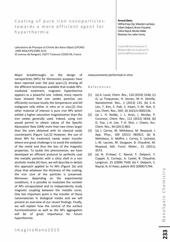
I m a g i n e N a n o 2 0 1 5
Na
no
Sp
ain
Ch
em
ist
ry
23
3
C o a t i n g o f p u r e i r o n n a n o p a r t i c l e s :
t o w a r d s a m o r e e f f i c i e n t a g e n t f o r
h y p e r t h e r m i a
Laboratoire de Physique et Chimie des Nano-Objets (LPCNO)
UMR INSA/UPS/CNRS 5215
35 avenue de Rangueil, 31077 Toulouse CEDEX 04, France
Major breakthroughs on the design of
nanoparticles (NPs) for theranostic purposes have
been reported over the past years.[1] Among all
the different techniques available that enable NPs-
mediated treatment, magnetic hyperthermia
appears as a powerful one. Indeed, many reports
have showed that iron oxides particles can
efficiently increase locally the temperature and kill
malignant cells either in vitro or in vivo.[2] One
other material of interest is pure iron NPs which
exhibit a higher saturation magnetization than the
iron oxides generally used. Indeed, using iron
would permit to obtain values of the Specific
Absorption Rate (SAR) more than two times larger
than the ones obtained with its classical oxide
counterparts (Figure 1a).[3] However, the use of
these NPs for treatment needs water transfer
where one great challenge is to avoid the oxidation
of the metal and thus the loss of the magnetic
properties. To tackle this phenomenon, we have
developed an efficient protocol to perfectly coat
the metallic particles with a silica shell in a non
alcoholic media.[4] Here, we will describe in details
this approach applied to Fe NPs (Figure 1b) and
show that whatever the thickness of the coating,
the iron core of the particles is preserved.
Moreover, depending on the experimental
conditions, it is possible to modulate the number
of NPs encapsulated and to independently study
magnetic coupling between the metallic cores.
One last important point is the transfer of these
nanomaterials in biological media and we will
present an overview of our recent findings. Finally,
we will explain how the control of the surface
functionalization as well as the NPs aggregation
will be of great importance for future
hyperthermia
measurements performed in vitro.
R e f e r e n c e s
[1] (a) A. Louie, Chem. Rev., 110 (2010) 3146; (c)
Q. Le Trequesser, H. Seznec, M.-H. Delville,
Nanotechnol. Rev., 2 (2013) 125. (b) E.-K.
Lim, T. Kim, S. Paik, S. Haam, Y.-M. Huh, K.
Lee, Chem. Rev., DOI: 10.1021/cr300213b.
[2] (a) L. H. Reddy, J. L. Arias, J. Nicolas, P.
Couvreur, Chem. Rev., 112 (2012) 5818; (b)
D. Yoo, J.-H. Lee, T.-H. Shin, J. Cheon, Acc.
Chem. Res., 44 (2011) 863.
[3] (a) J. Carrey, M. Mehdaoui, M. Respaud, J.
App. Phys., 109 (2011) 083921; (b) B.
Mehdaoui, A. Meffre, J. Carrey, S. Lachaize,
L.-M. Lacroix, M. Gougeon, B. Chaudret, M.
Respaud, Adv. Funct. Mater., 21 (2011),
4573.
[4] (a) N. El-Hawi, C. Nayral, F. Delpech, Y.
Coppel, A. Cornejo, A. Castel, B. Chaudret,
Langmuir, 25 (2009) 7540; (b) F. Delpech, C.
Nayral, N. El-Hawi, patent WO 2009071794.
Arnaud Glaria,
Wilfried Sojo Ojo, Sébastien Lachaize,
Fabien Delpech, Bruno Chaudret,
Céline Nayral, Nicolas Hallali,
Reasmey Tan, Julian Carrey
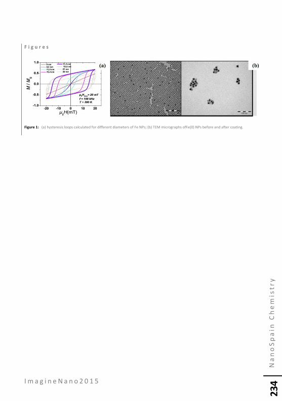
I m a g i n e N a n o 2 0 1 5
Na
no
Sp
ain
Ch
em
ist
ry
23
4
F i g u r e s
Figure 1: (a) hysteresis loops calculated for different diameters of Fe NPs; (b) TEM micrographs ofFe(0) NPs before and after coating.

I m a g i n e N a n o 2 0 1 5
Na
no
Sp
ain
Ch
em
ist
ry
23
5
A d v a n c e s i n o n - s u r f a c e s y n t h e s i s
The NanoSciences Group, CEMES-CNRS, 29 Rue Marvig 31055 Toulouse,
France
In less than a decade, on-surface synthesis by
covalent coupling of reactive precursors adsorbed
on metallic, semi-conducting or insulating films has
emerged as a powerful approach for the
fabrication of novel molecular architectures with
potential applications in nanoelectronics,
optoelectronics and other fields where new low-
dimensional materials with tailored properties are
needed [1 , 2].
Using this bottom-up route, atomically precise
grapheme nanoribbons,
polyphthalocyanines films, metal
coordination frameworks,
porous metal networks,
superhoneycomb frameworks,
etc. have been synthesized.
We will introduce current
developments in this field such
as new reactions, mechanisms,
optimization of the syntheses, semi-conducting
surfaces and perspectives [2].
Recent advances of thermally or photochemically
activated coupling reactions on bulk insulators that
have opened new avenues for molecular
electronics and the fabrication of molecular logic
gates will also be presented.
R e f e r e n c e s
[1] G.Franc and A.Gourdon, Phys. Chem. Chem.
Phys. 13, (2011)14283–14292.
[2] J. Méndez, M. Francisca López and José A.
Martín-Gago, Chem. Soc. Rev. 40, (2011) 4578-
4590.
[3] “On-surface chemistry”in “Advances in Atom
and Single Molecule Machines”, Springer
Series Ed. A. Gourdon (2016) In the press.
[4] R. Lindner, P. Rahe, M. Kittelmann, A.
Gourdon, R. Bechstein, and A.Kühnle, Angew.
Chem. Int. Ed. Engl. 53, (2014) 7952-7955
F i g u r e s
Figure 1: Surface controlled polymerization of a C60 monolayer on
calcite [3]
André Gourdon

I m a g i n e N a n o 2 0 1 5
Na
no
Sp
ain
Ch
em
ist
ry
23
6
L i g h t - c o n t r o l l e d s e l f - a s s e m b l y o f n o n -
p h o t o r e s p o n s i v e n a n o p a r t i c l e s
Department of Organic Chemistry, Weizmann Institute of Science,
Rehovot 76100, Israel
The ability to reversibly guide the assembly of
nanosized objects with external stimuli, in
particular light, is of fundamental importance, and
it contributes to the development of applications
as diverse as nanofabrication [1] and controlled
drug delivery [2]. However, all systems described
to date are based on nanoparticles that are
inherently photoresponsive, which makes their
preparation cumbersome, and can significantly
hamper their performance [3]. Here, we describe a
conceptually new methodology to reversibly
assemble nanoparticles using light, which does not
require that the particles be functionalized with
light-sensitive ligands. Our strategy is based on the
use of a photoswitchable medium that responds to
light in such a way that it modulates the
interparticle interactions. Nanoparticle assembly
proceeds quantitatively and without apparent
fatigue in solution as well as in gels. Exposing the
gels to light in a spatially controlled manner
allowed us to draw images that spontaneously
disappeared after a specific period of time.
R e f e r e n c e s
[1] Nie, Z. H.; Petukhova, A.; Kumacheva, E. Nat.
Nanotech. 5 (2010), 15.
[2] Sun, C.; Lee, J. S. H.; Zhang, M. Q. Adv. Drug
Deliv. Rev. 60 (2008), 1252.
[3] Klajn, R.; Stoddart, J. F.; Grzybowski, B. A.
Chem. Soc. Rev. 39 (2010), 2203.
Rafal Klajn

I m a g i n e N a n o 2 0 1 5
Na
no
Sp
ain
Ch
em
ist
ry
23
7
H y b r i d i n o r g a n i c - ( b i o ) o r g a n i c
m a t e r i a l s t h r o u g h m o l e c u l a r l e v e l
m o d i f i c a t i o n w i t h v a p o r - p h a s e
i n f i l t r a t i o n 1CIC nanoGUNE, 20018 Donostia-San Sebastian,Spain
2Centrode Física de Materiales, Material PhysicsCenter, 20018
Donostia-San Sebastian, Spain 3IKERBASQUE, Basque Foundation for Science, 48011 Bilbao, Spain
Polymeric materials of various types are
anticipated being the most important building
blocks for future applications. The reasons lie in
their established processes for mass production in
various shapes, mechanical flexibility for easy
handling, compatibility for roll-to-roll production
processes, versatility in functionalization, etc.
While for many applications synthetic polymers
are still without alternative, manyapproaches seek
for a sustainable substitute, whenever suitability is
given.
Cellulose represents the most abundant
biopolymers on Earth and is the fundamental
building block of plants and their subsequent
products such as paper and cotton. Furthermore
recent and significant interest has been expressed
in using cellulose based materials in a wide variety
of applications, in everything from
supercapacitors, batteries, and solar cells, to
advanced functional filters in waste water
treatment, and even wearable electronics. Several
techniques have been proposed for the
functionalization of these next generation
materials including, sol-gel, CVD, etc.However, one
of the most promising techniques is atomic layer
deposition (ALD).ALD is a similar, though
chemically distinct, form of CVD that allows low
temperature deposition, often below 100°C,
monolayer material growth, and extreme
conformality over even the most stringent
geometries. A recent modification to ALD, termed
vapor phase metal infiltration, allows for molecular
scale modification of a variety of biological and
syntheticsubstrates and scaffolds including; spider
silk, collagen, porphyrins, and
polytetrafluoroethylene (PTFE) towards and
entirely new class of hybrid materials. As well
asamore detailed understanding of the reaction
between these organic substrates and the metal-
organic precursors commonly used in standard
ALD processes.
Here we report the modification of a variety of
polymers, including spider silk, collagen, PTFE,
Kevlar, cellulose and cotton with common ALD
precursors, trimethyl aluminum and diethyl zinc.
Our findings show that the precursors induce
small, but important changes to the polymer upon
chemical interaction and that each precursorhas
different potential reaction pathways. For
characterization a variety of methods have been
applied, including FTIR, XRD, NMR, XPSand Raman
spectroscopy. We also discuss how these small
molecular scale changes lead to large changes in
the bulk mechanical properties of the substrates as
studied through uniaxial tensile testing. These
experiments point at the possibility of using this
infiltration method to alter the properties of the
materials by hybridizing inorganic ceramics with a
polymeric substrate.
K.E. Gregorczyk1, M. Garcia
1,
I. Azpitarte1, D. Pickup
2, C. Rogero
2,
and M. Knez1,3
I m a g i n e N a n o 2 0 1 5
Na
no
Sp
ain
Ch
em
ist
ry
23
8
P r o t e o l y t i c d i g e s t i o n o f b o v i n e
s u b m a x i l l a r y m u c i n ( B S M ) a n d i t s
i m p a c t s o n a d s o r p t i o n a n d l u b r i c i t y a t
a h y d r o p h o b i c s u r f a c e
1Technical University of Denmark, Department of Mechanical Engineering, DK-2800
Kgs. Lyngby, Denmark, 2Enzyme and Protein Chemistry, Department of Systems Biology, Technical University
of Denmark, DK-2800 Kgs. Lyngby, Denmark
Mucin is the major constituent of the mucous
secretions that cover epithelial surfaces exposed
to the environment in human/animals. The
primary function of mucous gels is known to
provide protection to epithelial surfaces from
invasive microbes and physical insults by forming a
lubricating layer. About 50 to 80% of the molecular
weight of mucin is attributed from post-
translational N- and O-linked glycosidic
modifications. The ability of the glycosidic
modifications to retain water at the epithelial
surface facilitates lubrication. N- and C-terminal
interactions and also entanglement of the
glycosidic modifications lead to a viscoelastic
material that offers excellent lubrication
properties [1-4]. Since mucins are composed of
various biochemical functional moieties, it is
expected that biochemical treatments of mucins
lead to alteration in the structure, conformation,
capabilities to adsorb onto engineering material
surfaces, and consequently lubricity. In this study,
proteolytic digestion on bovine submaxillary mucin
(BSM) and its impacts on the size, structure,
surface adsorption, and lubricating properties
were studied. Two proteases with distinctly
different cleavage specificities, namely trypsin and
pepsin, were employed. SDS-PAGE analysis using
two staining methods showed that only the
unglycosylated terminal regions of BSM were
degraded by the proteases and the central,
glycosylated regions remain nearly unaffected. Size
exclusion chromatography (SEC) and dynamic light
scattering (DLS) studies indicated that tryptic
digestion mainly led to the reduction in size,
whereas pepsin digestion rather led to the
increase in size of BSM. Less complete cleavage of
terminal peptides by pepsin and subsequent
aggregation between BSMs were thought to be
responsible for the increased size. Far-UV circular
dichroism (CD) spectra of the protease-treated
BSMs showed a slight change in the secondary
structure owing to the removal of terminal
domains, but the overall random coil structural
conformation by the central glycosylated regions
remained dominant and essentially unchanged.
Surface adsorption properties as characterized by
optical waveguide lightmode spectroscopy (OWLS)
showed that tryptic and pepsin digestion of BSM
resulted in a decrease and a slight increase in the
adsorbed mass onto a hydrophobic surface
(polydimethylsiloxane (PDMS)), respectively,
compared to intact BSM. This is related to the
partial preservation of peptide residues after
pepsin digestion as confirmed by SEC and DLS
studies. Despite a contrast in the adsorbed amount
of the protease-treated BSMs onto the PDMS
surface, both proteases substantially deteriorated
the lubricating capabilities of BSM at the self-
mated sliding interface of PDMS. The present
study supports the notion that the terminal
domains of BSM are critical to the adsorption and
lubricating properties of BSM at hydrophobic
interfaces.
R e f e r e n c e s
[1] J.B. Madsen, K.I. Pakkanen, L. Duelund, B.
Svensson, M. Abou Hachem, S. Lee, Prep.
Biochem. Biotech, 45 (2015) 84-99.
[2] N. Nikogeorgos, J.B. Madsen, S. Lee, Coll. Surf.
B: Biointerfaces, 122 (2014) 760-766.
[3] J. Sotres, J.B. Madsen, T. Arnebrand, S. Lee, J
Coll. Interf. Sci. 428 (2014), 242-250.
[4] N. Nikogeorgos, P. Efler, A.B. Kayitmazer, . S.
Lee, Soft Matter 11 (2015), 489-498
Seunghwan Lee,1
Jan Busk Madsen,1 Birte Svensson,
2
Maher Abou Hachem2

I m a g i n e N a n o 2 0 1 5
Na
no
Sp
ain
Ch
em
ist
ry
23
9
M u l t i d i m e n s i o n a l c h a r a c t e r i z t i o n o f
G r a p h e n e a t u l t r a l o w t e m p e r a t u r e s
Rachel and Selim Benin School of Engineering and Applied Science, The Hebrew
University of Jerusalem and 2Nanonics Imaging Ltd, Jerusalem, Israel
(www.nanonics.co.il)
It is a challenge to study 2D materials, such as
Graphene, MoS2, WeSe2, etc. at temperatures
down to 10oK when one considers the wide variety
of physical phenomena that have to be applied to
get a full picture of the functionality of these
materials. A variety of properties of these 2D
materials are important to understand at low
temperature including their chemistry (Raman),
structure, nanoscale photoconductivity, electrical
and thermal properties, and near-field optical. The
ability to simultaneously measure these properties
is especially important so that correlations and
interactions between these properties at these low
temperatures can be understood. All of these
phenomena are common not only to 2D materials
but also to carbon nanotubes and related
nanomaterials.
This presentation will describe the development of
cryogenic multiple SPM probe instrumentation to
probe this variety of properties of graphene and
other 2D materials. The system that will be
described has a completely free optical axis from
above and below that is not obscured by electrical
or other probes. This design permits on-line AFM-
Raman and Tip Enhanced NanoRaman Scattering
(TERS). With such a system we have investigated
graphene and HfO2 using multiprobe electrical,
Kelvin probe, NSOM and on-line Raman. The
results have yielded new insights into the chemical
changes that are correlated to the electrical
conductivity.
Aaron Lewis, Oleg Zinoviev,
Anatoly Komissar, Eran Maayan
and David Lewis

I m a g i n e N a n o 2 0 1 5
Na
no
Sp
ain
Ch
em
ist
ry
24
0
H i g h l y S y m m e t r i c M u l t i d e n t a t e
L i g a n d s f o r C a t a l y s i s a n d F u n c t i o n a l
M a t e r i a l s Dipartimento Scienze Chimiche, Università di Padova, Via Marzolo 1,
35131, Padova, Italy
The use of modular, multidentate ligands is one of
the current trends in catalyst design. Advantages
include the high stability of the corresponding
metal complexes, which often allows low catalyst
concentrations without loss of catalyst integrity.
Secondly, a nearly complete filling of all
coordination sites of the metal by a single ligand
reduces the chances of formation of multimeric
and often undefined metal-species under catalytic
conditions. The presence of only a single
catalytically active species greatly facilitates
mechanistic studies and catalyst optimization. In
the last years our group has been involved in the
study of early transition metal complexes with
triphenolate ligands and their application in
catalysis.[1,2]
In this communication, we will report on most
recent results related to the effective post
modifications of the ligand backbones that allow
obtaining supramolecular hybrid functional
systems with dimensions spanning from single
molecules to much larger aggregates. In particular,
the synthesis and characterization of novel
systems bearing multiple ion-TAGs, gelator,
fluorescent or organic radical residues will be
described together with preliminary results of
applications in catalysis and functional materials
R e f e r e n c e s
[1] G. Licini, M. Mba, C. Zonta, Dalton Trans.27,
(2009) 5265; M. Mba, C. Zonta, G. Licini
(2014) “Coordination chemistry and
applications of nitrilotris (N-
methylenephenoxy)-metal complexes” in
Patai’s Chemistry of Functional Groups,
edited by I. Marek. John Wiley & Sons, Ltd:
Chichester, UK.
[2] C. Zonta, G. Licini Chem. Eur. J., 29, (2013)
9438 and reference therein
F i g u r e s
Giulia Licini

I m a g i n e N a n o 2 0 1 5
Na
no
Sp
ain
Ch
em
ist
ry
24
1
C o v a l e n t g r a f t i n g e f f e c t s o n t h e
t h e r m a l p r o p e r t i e s o f r e n e w a b l e
P o l y ( L - l a c t i d e ) / c e l l u l o s e n a n o c r y s t a l
n a n o c o m p o s i t e s
1 Macromolecular Chemistry Research Group. Dept. of Physical Chemistry. Faculty of
Science and Technology. University of the Basque Country (UPV/EHU), Leioa 48940,
Spain. 2Basque Center for Materials, Applications and Nanostructures (BCMaterials), Parque
Tecnológico de Bizkaia, Ed. 500, Derio 48160, Spain.
Poly(L-lactide) (PLLA) is a semicrystalline
thermoplastic which belongs to a biocompatible,
biodegradable and bioresorbable polymers. PLLA
also fulfills many requirements of the traditional
non-biodegradable packaging materials and it is
therefore considered of great value from an
ecological point of view due to its biobased
character. Nonetheless, there are several aspects
such as its slow crystal growth rate, its marked
physical aging when used in ambient conditions
and its poor thermal stability which limit the use of
PLLA as a commodity plastic [1].
Nanocomposite approach could be viewed as an
efficient strategy to overcome the aforementioned
drawbacks. In accordance with the 12 Principles of
Green Chemistry [2], which underline the basis to
develop ecologically friendly materials, in this work
fully renewable PLLA nanocomposites have been
obtained. Among all the available naturally-
occurring nanoreinforcements, the rod-like
cellulose nanocrystals (CNC) are of special interest
due to their outstanding mechanical properties,
low density, low cost and its huge potential for
chemical modification. Unfortunately, its strong
hydrogen self-association behaviour in nonpolar
systems makes CNC difficult to disperse, reducing
their efficiency as reinforcing phase. In this sense,
grafting-from approach has been carried out with
the aim of improving the interfacial adhesion and
CNC dispersion within the polymer matrix. PLLA
chains are initiated from the surface hydroxyl
groups of CNC by a surface-initiated ring opening
polymerization (SI-ROP) [3].
Results show the crystallization rate is increased by
1.7-5 times in presence cellulose nanocrystals.
Additionally, structural relaxation kinetics of PLLA
chains has been drastically reduced by 53% and
27% with the addition of neat and grafted CNC
respectively. Those results suggest that neat CNC
reduce structural relaxation of bulk material to a
greater extent than grafted CNC because of the
reduction of the available PLLA/CNC interfaces
given by SI-ROP process. The thermal degradation
activation energy (E) determined from
thermogavrimetric analysis reveal a reduction on
the thermal stability when in presence of CNC-g-
PLLA, while raw CNC slightly increases the thermal
stability of PLLA. Those results confirm that the
presence of residual catalyst in CNC-g-PLLA plays a
pivotal role in the thermal degradation behavior of
nanocomposites. In this framework, the
improvement of the SI-ROP process would be the
next important step towards the development of
renewable materials with enhanced functional
properties.
R e f e r e n c e s
[1] E Lizundia, JR Sarasua, Macromolecular
Symposia 321 (2012) 118.
[2] PT Anastas, JC Warner, Green Chemistry:
Theory and Practice; Oxford University Press,
148 (1998).
[3] A Dufresne, Materials Today, 13 (2013) 220.
E. Lizundia1,
J. L. Vilas2, L. M. León
1

I m a g i n e N a n o 2 0 1 5
Na
no
Sp
ain
Ch
em
ist
ry
24
2
F i g u r e s
Figure 1: Scheme showing surface-initiated ROP of L-lactide (L-LA) to obtain CNC-g-PLLA+(Sn(Oct)2).

I m a g i n e N a n o 2 0 1 5
Na
no
Sp
ain
Ch
em
ist
ry
24
3
N o v e l S o l i d P h a s e s b y S e l f - A s s e m b l i n g
o f N a n o c l u s t e r s
1Kimika Fakultatea, Euskal Herriko Unibertsitatea (UPV/EHU) and Donostia
International Physics Center (DIPC), PK 1072, 20080 Donostia, Euskadi (Spain)
The theoretical search for novel polymorphs of
inorganic compounds have increased significatively
in the last years. One of the routes to build such
compounds is the so-called nanocluster
assembling, where nanometer-sized structures are
used as building blocks for the formation of 3D
periodic systems. Hollow cage-like structures are
ideal candidates for such assembling, resembling
the case of carbon fullerenes in fullerites.
In this work we focus on the assembling of bare
and endohedrally doped hollow nanoclusters of II-
VI materials, concretely, ZniSi and CdiSi, (i=12,16)
which were predicted to be
the global minima. The
considered dopant atoms
were several alkali metals,
halogens and transition
metals [1-3].
Different polymorphs were
characterized for all cases
[4,5]. Most of them were
stable towards vibration. In addition to phonon
calculations, quantum molecular dynamics
simulations, E vs V calculations were carried out in
order to provide some theoretical evidence of the
metastability of these compounds. In Figure 1, one
of the characterized metastable structure, FAU, is
shown.
R e f e r e n c e s
[1] E. Jimenez-Izal, J. M. Azpiroz, R. Gupta, J. M.
Matxain, J. M. Ugalde, J. Mol. Model. 20,
(2014) 2227.
[2] E. Jimenez-Izal, J. M. Matxain, M. Piris, J. M.
Ugalde, Comput. 1 (2013) 31.
[3] E. Jimenez-Izal, J. M. Matxain, M. Piris, J. M.
Ugalde, J. Phys.l Che. C 115, (2011) 7829.
[4] E. Jimenez-Izal, J. M. Matxain, M. Piris, J. M.
Ugalde, Phys. Chem. Chem. Phys. 14 (2012)
9676.
[5] J. M. Matxain, M. Piris, X. Lopez, J. M. Ugalde,
Chem. Eur. J. 15 (2009) 5138.
F i g u r e s
Figure 1: Characterized metastable FAU polymorph build by
Cd12S12 clusters.
Jon M. Matxain1
I m a g i n e N a n o 2 0 1 5
Na
no
Sp
ain
Ch
em
ist
ry
24
4
L i p i d n a n o p a r t i c l e s a s d e l i v e r y v e h i c l e
f o r b i o - m a c r o m o l e c u l e s
1Univ. Grenoble Alpes, Grenoble, F-38000, France;
2CEA, LETI MINATEC, Technologies for Healthcare and Biology Division, 17 rue des
martyrs, 38054 Grenoble Cedex 9, France 3Institut Albert Bonniot - UJF/INSERM U823, Rond-point de la Chantourne,
38042 Grenoble Cedex 9, France.
Nanomedicine, the application of nanotechnology
to medicine, is a growing field for decades. Several
nanoparticles are already on the market, especially
for tumour diagnosis or therapy. Their applications
are based on their ability to reach the tumour
tissue due to the well-known “enhanced
permeability and retention” (EPR) effect where
they can accumulate locally in the tumour and
increase thus the efficiency of their contents. Most
of these drugs are hydrophobic small molecule
compounds whereas new therapeutic strategies in
development are basedon larger molecules from
biological origin such as peptides, proteins or
nucleic acids. Novel nanoparticle formulations are
now highly anticipated for delivery of these bio-
macromolecules, in particular for applications
beyond cancer therapy. We designed lipid
nanoparticles able to deliver either nucleic acids,
or antigen proteins. A panel of chemical strategies
have been explored for loading the bio-
macromolecules into/onto the particles, ranging
from simple electrostatic interaction to covalent
grafting by using modified polymers. The resulting
particles presented not only a high colloidal
stability, but also a good safety profile. Moreover,
their efficacy for the concerned applications were
improved either to transfect nucleic acids into cells
or to elicit immune responses in mice whenever
the protein antigens are coupled to the
nanoparticles. Further preclinical evaluation of
these particles containing bio-macromolecules in
different animal models is now ongoing and will
contribute to their successful clinical translation.
Jessica Morlieras1,2
, Alan Hibbitts1,2
,
Thomas Courant1,2
, Emilie Bayon1,2
,
Hei Lanne Reynaud3,Christian
Villiers3, Mathilde Menneteau
1,2,
Patrice Marche3
and Fabrice Navarro1,2

I m a g i n e N a n o 2 0 1 5
Na
no
Sp
ain
Ch
em
ist
ry
24
5
T h e E q u i v a l e n t C i r c u i t s o f M o l e c u l a r
T u n n e l J u n c t i o n s
Chemistry Depart of the National University of Singapore
Department of Chemistry, 3 Science Drive 3, Singapore 117543
Molecular junctions of the form of electrode–
SAM–electrode(SAM=self-assembled monolayer)
are appealing because of their potential of
inducing, and controlling, electronic function at the
nanometer length scales.[1,2]Understanding the
nature of the molecule-electrode contacts in these
two-terminal junctions is crucial but it is mostly
poorly understood.[3]The reason is the electrical
properties of electrode–SAM–electrode junctions
are usually studied by two-terminal DC
measurements which only determine the total
current(impeded by all components of the
junction) as a function of applied bias. Hence,
these methods do not distinguish the contributions
of each component (the SAM, the electrodes, and
the two SAM–electrode interfaces)to the
measured current and are not suitable to measure
the dielectric response.
Recently we showed that impedance spectroscopy
makes it possible to isolate the contribution of
each component in the junctions to the total
impedance of EGaIn based junctions(Figure
1).[4,5]Here I will present that temperature
dependent and potentiodynamic impedance
spectroscopy make it possible to elucidate the bias
and temperature dependency of each circuit
component(contact resistance, SAM resistance,
and the capacitance of the SAM)of two-terminal
SAM-based junctions, unlike DC measurements,
independently from each other. We found that the
metal–electrode contact resistance is independent
of the temperature or applied bias and more than
4 orders of magnitude smaller than the thinnest
SAM measured, the thin conductive oxide layer
plays an insignificant role. We also find that by
introducing large polarizable atoms the dielectric
response can be engineered at the molecular level.
We believe that impedance spectroscopy as a
function of temperature and applied bias is a
useful and complementary tool to DC
measurements to elucidate how each component
of two-terminal SAM-based junctions impedes
charge transfer and it opens the door to
investigate dielectric response in 2-terminal
junctions at the molecular scale.
R e f e r e n c e s
[1] Nerngchanmnong, N.; Yuan, L.; Qi, D. C.;
Jiang, L.; Thompson, D.; Nijhuis, C. A. Nature
Nanotechnol.2013, 8, 113.
[2] Tan, S. F., Wu, L., Yang, K. L. W., Bai, P.,
Bosman, M., Nijhuis, C. A. Science, 2014, 343,
1496.
[3] Yuan, L.; Nerngchamnong, N.; Li, J.; Qi, D.-C.;
Hamoudi, H.; del Barco, E.; Roemer, M.;
Sriramula, R. K.; Thompson, D.; Damien
Thompson; Nijhuis, C. ANat. Commun.2015,
6, 6324.
[4] Wan, A.; Jiang, L.; Suchand Sangeeth, C. S.;
Nijhuis, C. A. Adv. Funct. Mater.201424,
4442.
[5] Suchand, S.S.C.; Wang, A.; Nijhuis, C.A. J. Am.
Chem. Soc.2014, 136, 11134–11144. Heitzer,
H. M.; Marks, T.J.;Ratner,M.A. ACS Nano,
2014, 8, 12587.
Christian A. Nijhuis
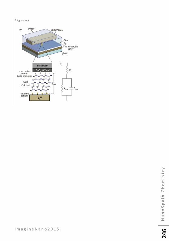
I m a g i n e N a n o 2 0 1 5
Na
no
Sp
ain
Ch
em
ist
ry
24
6
F i g u r e s

I m a g i n e N a n o 2 0 1 5
Na
no
Sp
ain
Ch
em
ist
ry
24
7
P r o t e i n a n d P e p t i d e C h e m i s t r y f o r
N a n o t e c h n o l o g y : B i o m i n e r a l i z a t i o n ,
C r y s t a l l i z a t i o n , P a t t e r n i n g a n d S e l f -
o r g a n i z a t i o n
1CIC nanoGUNE, 20018, Donostia-San Sebastian, Basque Country, Spain
2Universidad del Pais Vasco (UPV/EHU), 48940, Leioa, Basque Country, Spain
3Ikerbasque, Basque Foundation for Science, 48011, Bilbao, Basque Country, Spain
In biology, a huge number of protein and peptide
molecules established self-organizing systems with
sophisticated abilities, for example, detection of
light by our eyes, and detection of sound by our
ears. Therefore, our world can utilize such
biomolecules to develop more complex structures
for nanotechnology. On the way, we have
developed fabrication methods for inorganic NPs
and the assembly of the NPs, based on structure
and function of proteins and peptides
Biomineralization is one of the processes to build
bio-inorganic materials such as bone and teeth.
Some proteins can generate inorganic material
through specific aminoacid sequences,distributed
in protein structures, which enable us to use them
as bio-cargos for NPs .For example, the cage shape
protein Dps (DNA binding protein in starved cell,
diameter: 12 nm) can form metal oxide NPs with in
its cavity (diameter 5 nm)by assembling iron ions
and nucleating NPs at specific sites[1].The NP
species can be changed by designing the synthesis
solution, allowing for the fabrication of artificial
NPs. There are many types of cage-shaped
proteins in nature, such as ferritin and virus
capsids (Fig.1).In addition, tube-shaped viruses
such as TMV (Tobacco Mosaic Virus, inner
diameter: 4nm) can be used to fabricate rod-
shaped in organic NPs. Many types NPs and rods
have been fabricated in such cavities.
NPs containing bio-cargo scan self-assemble into
two-or three-dimensional crystals through protein-
protein interactions based on typical crystallization
techniques [2].In addition, the patterning of NPs
can be optimized with bio-cargos functionalized
using specific peptides. Peptides with certain
biochemical functions can recognize the surface of
specific inorganic materials [3]. A bio-cargo that is
functionalized with such a peptide can be
patterned on a surface of a target material. These
protein and peptide techniques have been utilized
to develop a range of devices [3].
In this talk, we will also show how to design self-
organization systems through bio-cargo structures,
and affinity peptides to fabricate complex NP
structures.
R e f e r e n c e s
[1] Mitsuhiro Okuda, et al. NanoSpain Bio&Med,
ImagineNano, (2015) poster.
[2] Mitsuhiro Okuda et al. Chem commun, 46
(2010) 8797.
[3] K.-I. Sano, et al. Langmuir, 29 (2013) 12483.
F i g u r e s
Figure 1.Schematics of apoferritin (a) viewed from the four fold
symmetry axis. (b) shows the cavity.(c)Schematic drawing of Dps.
(d) Schematic drawing of CCMV.
Mitsuhiro Okuda1,3
, Kornelius Zeth2,3
and Alexander Bittner1,3

I m a g i n e N a n o 2 0 1 5
Na
no
Sp
ain
Ch
em
ist
ry
24
8
T h e Q u e s t f o r C h a r g e T r a n s p o r t i n
s i n g l e A d s o r b e d L o n g D N A - B a s e d
M o l e c u l e s
Institute of Chemistry and Center for Nanoscience and Nanotechnology
The Hebrew University of Jerusalem, 91904 Israel
DNA and DNA-based polymers have been at the
focus of molecular electronics owing to their
programmable structural versatility. The variability
in the measured molecules and experimental
setups, caused largely by the contact problem, has
produced a wide range of partial or seemingly
contradictory results, highlighting the challenge to
transport significant current through individual
DNA-based molecules. A well-controlled
experiment that would provide clear insight into
the charge transport mechanism through a single
long molecule deposited on a hard substrate has
never been accomplished. In this lecture I will
report on detailed and reproducible charge
transport in G4-DNA, adsorbed on a mica
substrate. Using a novel benchmark process for
testing molecular conductance in single polymer
wires, we observed currents of tens to over 100 pA
in many G4-DNA molecules over distances ranging
from tens to over 100 nm, compatible with a long-
range thermal hopping between multi-tetrad
segments. With this report, we answer a long-
standing question about the ability of individual
polymers to transport significant current over long
distances when adsorbed a hard substrate, and its
mechanism. These results may re-ignite the
interest in DNA-based wires and devices towards a
practical implementation of these wires in
programmable circuits.
R e f e r e n c e s
[1] "Direct measurement of electrical transport
through DNA molecules", Danny Porath,
Alexey Bezryadin, Simon de Vries and Cees
Dekker, Nature 403, 635 (2000).
[2] "Charge Transport in DNA-based Devices",
Danny Porath, Rosa Di Felice and Gianaurelio
Cuniberti, Topics in Current Chemistry Vol.
237, pp. 183-228 Ed. Gary Shuster. Springer
Verlag, 2004.
[3] “Direct Measurement of Electrical Transport
Through Single DNA Molecules of Complex
Sequence”, Hezy Cohen, Claude Nogues, Ron
Naaman and Danny Porath, PNAS 102, 11589
(2005).
[4] “Long Monomolecular G4-DNA Nanowires”,
Alexander Kotlyar, Nataly Borovok, Tatiana
Molotsky, Hezy Cohen, Errez Shapir and Danny
Porath, Advanced Materials 17, 1901 (2005).
[5] “Electrical characterization of self-assembled
single- and double-stranded DNA monolayers
using conductive AFM”, Hezy Cohen et al.,
Faraday Discussions 131, 367 (2006).
[6] “High-Resolution STM Imaging of Novel
Poly(G)-Poly(C)DNA Molecules”, Errez Shapir,
Hezy Cohen, Natalia Borovok, Alexander B.
Kotlyar and Danny Porath, J. Phys. Chem. B
110, 4430 (2006).
[7] "Polarizability of G4-DNA Observed by
Electrostatic Force Microscopy
Measurements", Hezy Cohen et al., Nano
Letters 7(4), 981 (2007).
[8] “Electronic structure of single DNA molecules
resolved by transverse scanning tunneling
spectroscopy”, Errez Shapir et al., Nature
Materials 7, 68 (2008).
[9] “A DNA sequence scanned”, Danny Porath,
Nature Nanotechnology 4, 476 (2009).
[10] “The Electronic Structure of G4-DNA by
Scanning Tunneling Spectroscopy”, Errez
Shapir, et.al., J. Phys. Chem. C 114, 22079
(2010).
Danny Porath

I m a g i n e N a n o 2 0 1 5
Na
no
Sp
ain
Ch
em
ist
ry
24
9
[11] “Energy gap reduction in DNA by
complexation with metal ions”, Errez Shapir,
G. Brancolini, Tatiana Molotsky, Alexander B.
Kotlyar, Rosa Di Felice, and Danny Porath,
Advanced Maerials 23, 4290 (2011).
[12] "Quasi 3D imaging of DNA-gold nanoparticle
tetrahedral structures", Avigail Stern, Dvir
Rotem, Inna Popov and Danny Porath, J. Phys.
Cond. Mat. 24, 164203 (2012).
[13] "Comparative electrostatic force microscopy
of tetra- and intra-molecular G4-DNA", Gideon
I. Livshits, Jamal Ghabboun, Natalia Borovok,
Alexander B. Kotlyar, Danny Porath, Advanced
materials 26, 4981 (2014).
[14] "Long-range charge transport in single G4-DNA
molecules", Gideon I. Livshits et. al., Nature
Nanotechnology 9, 1040 (2014).
F i g u r e s
I m a g i n e N a n o 2 0 1 5
Na
no
Sp
ain
Ch
em
ist
ry
25
0
R e c e n t p r o g r e s s o n p a t c h y
n a n o p a r t i c l e s a n d t h e i r d i r e c t i o n a l
b o n d i n g
1 CNRS, Univ. Bordeaux, CRPP, UPR 8641, F-33600 Pessac, France.
2Univ. Bordeaux, CNRS, ISM, UMR 5255, F-33405 Talence, France
3CNRS, Univ. Bordeaux, ICMCB, UPR 9048, F-33600 Pessac, France
Compared to standard fabrication methods based
on top-down approaches such as optical
lithography, colloidal self-assembly offers the
potential for easier fabrication and manipulation
of nano-and microstructures, especially in three
dimensions. In most cases, these building blocks
may not naturally assemble into any desired
structures. One emerging approach to confer
colloidal particles predetermined “instructions” for
assembly is to decorate the surface of the particles
with “sticky patches” made, for example, of
synthetic organic or biological molecules. This
strategy draws its inspiration in part from biology,
where the precision of self-assembled structures
such as viruses and organelles originates in the
selectivity of the interactions between their
constituents. In this talk, we report on a new route
to synthesize patchy nanoparticles with a
controlled number of patches or dimples as well as
on their potential use as building blocks for the
elaboration of new supracolloids with unusual
morphology and optical properties.
The so-patchy particles were derived from colloidal
molecules [1] made of a central silica
coresurrounded by a precise number, n, of
polystyrene satellite nodules [2,3].We succeeded
in promoting the growth of the silica core of these
colloidal molecules. While growing, the silica
surface conforms to the shape of the PS nodules.
After functionalization of the inter-nodule surface
area and dissolution of the polystyrene nodules,
homogeneous batches of silica particles with n
well-located patches at their surface can be
produced in large quantities [4]. The patchy
character of the silica particles was evidenced by
TEM characterization (see Figure). The controlled
assembly of patchy nanoparticles offers the unique
capability of creating new supraparticles [5]or
superlattice structures. We will present some
recent results on the self-assembly of the
multivalent silica nanoparticles.
These patchy particles can also be used for
creating new nano-objects suitable for many
applications such as sensing, metamaterials,
photonics, etc. For example, they can be used to
elaborate nanocages of noble metal with a
controlled number of holes
R e f e r e n c e s
[1] E. Duguet, A. Désert, A. Perro and S. Ravaine,
Chem. Soc.Rev.40(2011) 941
[2] A. Perro, E. Duguet, O. Lambert, J. C. Taveau,
E. Bourgea-Lami and S. Ravaine, Angew.
Chem.,Int. Ed.48(2009) 361.
[3] A. Désert, I. Chaduc, S. Fouilloux, J.C. Taveau,
O. Lambert, M. Lansalot, E. Bourgeat-Lami, A.
Thill, O. Spalla, S. Ravaine and E. Duguet,
Polym. Chem.3(2012)1130
[4] A. Désert, C. Hubert, Z. Fu, L. Moulet, J.
Majimel, P. Barboteau, A. Thill, M. Lansalot,
E. Bourgeat-Lami, E. Duguet and S. Ravaine,
Angew. Chem. Int. Ed.52 (2013)11068.
[5] C. Hubert, C. Chomette, A. Désert, M. Sun, M.
Treguer-Delapierre, S. Mornet, A. Perro, E.
Duguet and S.Ravaine, Faraday Discussions,
2015, DOI: 10.1039/C4FD00241E.
Serge Ravaine1, Céline Hubert
1,2,
Cyril Chomette3, Anthony Désert
3,
Adeline Perro-Marre2,
StéphaneMornet3, MonaTréguer-
Delapierre3, Etienne Duguet
3

I m a g i n e N a n o 2 0 1 5
Na
no
Sp
ain
Ch
em
ist
ry
25
1
F i g u r e s
Figure:TEM images of a) silica particles surrounded by 4 polystyrene satellite nodules, b) silica particles with 4 dimples and c) a dimpled silica
particle regioselectively decorated with gold nanoparticles [4]
I m a g i n e N a n o 2 0 1 5
Na
no
Sp
ain
Ch
em
ist
ry
25
2
S e n s i n g M o l e c u l e s a n d T e m p e r a t u r e a t
t h e N a n o s c a l e
University of Aveiro, Department of Chemistry
CICECO-Aveiro Institute of Materials, 3810-193 Aveiro, Portugal
In this talk I shall review some of the work carried
out in Aveiro in the last 6 years, or so, on the
design, synthesis and characterisation of
lanthanide (Ln) -bearing nanostructures for sensing
small molecules and temperature. Selected
examples of (i) nanoporous metal-organic
frameworks and silicates, and (ii) gold and Ln
oxides nanoparticles systems will be given.
Nanoporous metal-organic frameworks (MOFs) are
crystalline materials consisting of metal ions
bridged by organic linkers and exhibiting porosity
reminiscent of zeolites. Ln3+-organic frameworks
are very promising materials for tackling the
challenges in engineering of luminescent centres,
also presenting much potential as multifunctional
systems, combining light emission with properties
such as microporosity, magnetism, chirality,
molecule and ion sensing, catalysis and activity as
multimodal imaging contrast agents [1]. Only 10%
or so of MOFs are effectively nanoporous,
exhibiting zeolite-type behaviour, and
photoluminescent. The combination of porosity
and light emission allows the design of intriguing
new types of chemical species and temperature
sensors, which I shall highlight here [2-6].
In general, the thermal stability of MOFs is limited
and materials such as silicates present interesting
alternatives for certain applications. We have
recently reported a new Ln silicate orthorhombic
system, Na[(Gd1-aEua)SiO4], exhibiting
uncommon photoluminescence properties due to
structural disorder and a phase transition. This
system constitutes the first example of a
ratiometric thermometer based on a Ln3+ silicate,
particularly sensitive at cryogenic temperatures
(<100 K) [7].
While the use of plasmonic nanoparticles as
sources of heat have attracted much interest in
the last decade, research into ratiometric
nanothermometers with high-spatial resolution is
comparatively new. Suitable nanoplatforms
integrating heaters and thermometers, however,
have not been realized, despite their great
potential in nanophotonics and biomedicine. In
this talk I shall report a step forward towards
assessing the local temperature of laser-excited
gold nanostructures using an all-in-one
nanoplatform comprising (Gd,Yb,Er)2O3 nanorods
(thermometers, NR) that were surface-decorated
with gold nanoparticles (heaters, AuNPs) [8].
R e f e r e n c e s
[1] Rocha J., Carlos L. D., Paz F. A. A., Ananias D.,
Chem. Soc. Rev. 2011, 40, 926-940.
[2] Shi F. N., Cunha-Silva L., Ferreira R. A. S.,
Mafra L., Trindade T., Carlos L. D., Paz F. A. A.,
Rocha, J., J. Am. Chem. Soc. 2008, 130, 150-
167.
[3] Harbuzaru B. V., Corma A., Rey F., Atienzar P.,
Jordá J. L., García H., Ananias D., Carlos L. D.,
Rocha J., Angew. Chem. Int. Ed. 2008, 47,
1080-1083.
[4] Harbuzaru B. V., Corma A., Rey F., Jordá J. L.,
Ananias D., Carlos L. D., Rocha J., Angew.
Chem. Intl. Ed., 2009, 48, 6476-6479.
[5] Cadiau A., Brites C. D. S., Costa P. M. F. J.,
Ferreira R. A. S., Rocha J., Carlos L. D., ACS
Nano 2013, 7, 7213-7218.
[6] Abdelhameed R. M., Carlos L. D., Silva A.,
Rocha J., Chem. Commun. 2013, 49, (2013),
5019- 5021.
[7] Ananias, D., Almeida Paz, F. A., Yufit, D. S.,
Carlos, L. D., Rocha, J., J. Am. Chem. Soc.,
http://dx.doi.org/10.1021/ja512745y.
[8] 1) Debasu, M. L., Ananias, D., Pastoriza-
Santos, I., Liz-Marzan, L. M., Rocha, J., Carlos
L. D., Adv. Mater. 2013, 35, 4868-4874.
João Rocha
http://www.ciceco.ua.pt/jr

I m a g i n e N a n o 2 0 1 5
Na
no
Sp
ain
Ch
em
ist
ry
25
3
M e c h a n i c a l p r o p e r t i e s o f z i r c o n i u m
d i o x i d e a n d s i l i c o n n i t r i d e c o m p o s i t e s
Department of Metallurgical and Materials Engineering, Istanbul
Technical University, 34469 Maslak, Istanbul, Turkey
In this study, the mechanical properties of ZrO2-
Si3N4 composites containing 3.12 mass% MgO as a
stabilizer sintered at 1600˚C for 4 hr in a nitrogen
atmosphere has been investigated. XRD phase
analysis showed addition of Si3N4 destabilized
tetragonal zirconia phase and caused the
formation of monoclinic zirconia phase, also
zirconium oxide nitride phase was formed in the
sample with 10 and 15 mass% Si3N4 [1]. SEM
microstructure revealed that the grain size of the
specimens decreased with increasing content of
Si3N4. EDS analysis displays magnesium content
increased in the grain boundaries with adding
Si3N4. The results indicated that ZrO2 containing 10
and 15 mass% Si3N4 were performed higher
hardness values than stabilized zirconia[2]. The
room temperature mechanical properties of
flexural strength decreased with 5 mass% Si3N4
then increased with increasing Si3N4 content.
R e f e r e n c e s
[1] S. Berendts, M. Lerch, Journal of Crystal
Growth, 336 (2011) 106–111.
[2] S. Chockalingam, V. R.W. Amarakoon, Journal
of the Ceramic Society of Japan, 116 [6]
(2008) 700-705.
F i g u r e s
Sina Sadigh Akbari
Serdar Ozgen
I m a g i n e N a n o 2 0 1 5
Na
no
Sp
ain
Ch
em
ist
ry
25
4
B i o s y n t h e s i s o f S i l v e r N a n o p a r t i c l e s
a n d i t s A p p l i c a t i o n i n t h e R e m o v a l o f
M e r c u r y ( I I ) f r o m W a t e r
1Department of Earth Science, King Fahd University of Petroleum and minerals,
Dhahran 31261, Saudi Arabia 2Department of Chemistry, King Fahd University of Petroleum and minerals, Dhahran
31261, Saudi Arabia
The synthesis of nanoparticle using chemical
sources is gradually being replaced by bio-
synthesized nanoparticle to alleviate
environmental concerns posed by chemically
synthesized nanoparticle. Biosynthesized
nanoparticle continues to gain prominence in
various applications including water treatment.
This study is aimed at exploiting the amalgam
relationship between mercury and silver to
remove mercury from water samples. Local plant
leaves; Aloe vera and Basil are utilized in
synthesizing nanoparticles. They both showed
silver nitrate reduction capabilities to form silver
nanoparticles which were confirmed by UV-Visible
analysis. The biosynthesized nanoparticles were
characterized using Scanning Electron Microscopy
(SEM) and X-ray Diffraction (XRD). Mercury
removal was further carried out using porous
membranes functionalized silver nanoparticle
membrane filter and the analysis of mercury was
performed using cold vapour atomic fluorescence
spectroscopy.
R e f e r e n c e s
[1] I. Bhatt and B. N. Tripathi, Chemosphere, vol.
82, no. 3, Jan. (2011) pp. 308–17.
[2] B. Nowack and T. D. Bucheli, Environ. Pollut.,
vol. 150, no. 1, Nov. (2007) pp. 5–22.
[3] D. Ashok, Int. Res. J. Pharm., vol. 3, no. 2,
(2012) pp. 169–173.
[4] T. Yordanova, P. Vasileva, I. Karadjova, and D.
Nihtianova, Analyst, vol. 139, no. Mar. (2014)
6, pp. 1532–40.
[5] E. Bernalte, C. Marín Sánchez, and E. Pinilla
Gil, Anal. Chim. Acta, vol. 689, no. 1, Mar.
(2011) pp. 60–4.
[6] N. E. Selin, Annu. Rev. Environ. Resour., vol.
34, no. 1, Nov. (2009) pp. 43–63.
[7] D. K. Tiwari, J. Behari, and P. Sen, Water Res.,
vol. 3, no. 3, (2008) pp. 417–433.
[8] K. Leopold, M. Foulkes, and P. Worsfold,
Anal. Chim. Acta, vol. 663, no. 2, Mar. (2010)
pp. 127–38.
[9] K. Tyagi, J. Toxicol. Environ. Heal. Sci., vol. 5,
no. 9, Sep. (2013) pp. 172–177.
[10] E. K. Elumalai, T. N. V. K. V Prasad, J.
Hemachandran, and S. V. Therasa, J. of
Pharmaceutical Sci. Res., vol. 2, no. 9, (2010)
pp. 549–554.
[11] M. Vanaja, G. Gnanajobitha, K. Paulkumar, S.
Rajeshkumar, C. Malarkodi, and G.
Annadurai, J. Nanostructure Chem., vol. 3,
no. 1, (2013) p. 17.
1Salawu Adio Omobayo,
2Basheer Chanbsha

I m a g i n e N a n o 2 0 1 5
Na
no
Sp
ain
Ch
em
ist
ry
25
5
F i g u r e s
Figure 2: From left to right, Mixture of silver nitrate and plant
extract at 0, 15 and 30 minutes respectively.
Figure 3: UV- visible spectra of effect of time on the formation of
nanoparticles.
Figure 4: UV – Visible spectra of effect of broth concentration on
formation of AgNP.
Figure 5: UV- visible spectrum of the effect of different precursor
concentration on nanoparticles formed.
Figure 7: Effect of pH on formation of AgNP.
Figure 8: Biosynthesized AgNP at 2mM, 25oC, 1:25 broth
concentration, 20 minutes and pH 10.
Figure 10: SEM image of biosynthesized AgNP.
Figure 11: SEM image of biosynthesized AgNP.
Figure 12: Reaction of AgNP with 100pm mercury solution.
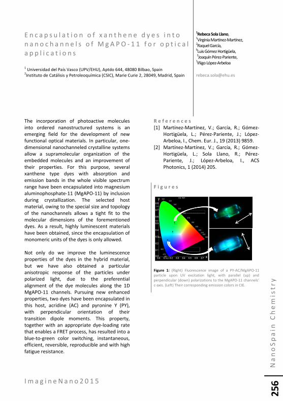
I m a g i n e N a n o 2 0 1 5
Na
no
Sp
ain
Ch
em
ist
ry
25
6
E n c a p s u l a t i o n o f x a n t h e n e d y e s i n t o
n a n o c h a n n e l s o f M g A P O - 1 1 f o r o p t i c a l
a p p l i c a t i o n s
1 Universidad del País Vasco (UPV/EHU), Aptdo 644, 48080 Bilbao, Spain
2Instituto de Catálisis y Petroleoquímica (CSIC), Marie Curie 2, 28049, Madrid, Spain
The incorporation of photoactive molecules
into ordered nanostructured systems is an
emerging field for the development of new
functional optical materials. In particular, one-
dimensional nanochanneled crystalline systems
allow a supramolecular organization of the
embedded molecules and an improvement of
their properties. For this purpose, several
xanthene type dyes with absorption and
emission bands in the whole visible spectrum
range have been encapsulated into magnesium
aluminophosphate-11 (MgAPO-11) by inclusion
during crystallization. The selected host
material, owing to the special size and topology
of the nanochannels allows a tight fit to the
molecular dimensions of the forementioned
dyes. As a result, highly luminescent materials
have been obtained, since the encapsulation of
monomeric units of the dyes is only allowed.
Not only do we improve the luminescence
properties of the dyes in the hybrid material,
but we have also obtained a particular
anisotropic response of the particles under
polarized light, due to the preferential
alignment of the dye molecules along the 1D
MgAPO-11 channels. Pursuing new enhanced
properties, two dyes have been encapsulated in
this host, acridine (AC) and pyronine Y (PY),
with perpendicular orientation of their
transition dipole moments. This property,
together with an appropriate dye-loading rate
that enables a FRET process, has resulted into a
blue-to-green color switching, instantaneous,
efficient, reversible, reproducible and with high
fatigue resistance.
R e f e r e n c e s
[1] Martínez-Martínez, V.; García, R.; Gómez-
Hortigüela, L.; Pérez-Pariente, J.; López-
Arbeloa, I., Chem. Eur. J., 19 (2013) 9859.
[2] Martínez-Martínez, V.; García, R.; Gómez-
Hortigüela, L.; Sola Llano, R.; Pérez-
Pariente, J.; López-Arbeloa, I., ACS
Photonics, 1 (2014) 205.
F i g u r e s
Figure 1: (Right) Fluorescence image of a PY-AC/MgAPO-11
particle upon UV excitation light, with parallel (up) and
perpendicular (down) polarizations to the MgAPO-11 channels’
c-axis. (Left) Their corresponding emission colors in CIE.
1Rebeca Sola Llano,
1Virginia Martínez-Martínez,
2Raquel García,
bLuis Gómez Hortigüela,
2Joaquín Pérez-Pariente,
1Iñigo López-Arbeloa

I m a g i n e N a n o 2 0 1 5
Na
no
Sp
ain
Ch
em
ist
ry
25
7
P h t h a l o c y a n i n e s a s c o m p o n e n t s o f
p h o t o v o l t a i c a n d a r t i f i c i a l
p h o t o s y n t h e t i c s y s t e m s
Organic Chemistry Department, Autonoma University of Madrid, Cantoblanco, Madrid,
28049, Spain and IMDEA Nanoscience, Cantoblanco, 28049-Madrid, Spain
Porphyrinoids are employed as components of
photovoltaic and artificial photosynthetic devices.
However, synthetic porphyrin analogues such as
phthalocyanines [1-3] have the advantage, as
photon harvesters, of exhibiting very high
extinction coefficients in a wavelength range that
extends to around 700 nm, where the maximum of
the solar photon flux occurs. Consequently, Pcs
have emerged as excellent light harvesting
antennas for incorporation into donor-acceptor
systems, mainly in connection with carbon
nanostructures as acceptor moieties.
Phthalocyanines (Pcs) constitute also promising
dyes as DSCphotosensitizers. [4]
On the other hand, Subphthalocyanines (SubPcs)
[5,6] are the lowest homologues of
phthalocyanines. Their pi-electron aromatic core
along with their non-planar cone-shaped structure
make them attractive compounds with singular
chemical and physical properties.
Subphthalocyanines are currently emerging as
excellent chromophoric systems for studying
electron and excitation transfer processes with
applications in photovoltaic devices.
During this talk an overview of the results obtained
by our group in Madrid will be given.
R e f e r e n c e s
[1] De la Torre, G.; Claessens, C.G.; Torres, T
Chem. Commun. 2007, 2000-2015.
[2] Martínez-Díaz, M. D.; de la Torre, G.; Torres,
T. Chem. Commun. 2010, 46, 7090-7108.
[3] Bottari, G.; de la Torre, G.; Guldi, D.M.;
Torres, T. Chem. Rev. 2010, 110, 6768– 6816.
[4] Ragoussi, M.E.; Cid, J.J.; Yum, J.H.; de la
Torre, G.; Di Censo, D.; Graetzel, M.;
Nazeeruddin, M.K.; Torres, T. Angew. Chem.
Int. Ed. Eng. 2012, 51, 4375 –4378.
[5] Claessens, C. G.; González-Rodríguez, D.;
Rodríguez-Morgade, M. S.; Medina, A.;
Torres, T. Chem. Rev., 2014,114, 2192-2277.
[6] Verreet, B.; Cheyns, D.; Heremans, P.;
Stesmans, A.;Zango, G.; Claessens, C. G.;
Torres, T.; Rand, B. P. Adv. Energy
Mater.2014, 4,(8) 201301413.
T. Torres, L. Tejerina , B.Kuhn,
W. A. Borzecka, D. P. Medina,
M. Medel, M.-E. Ragoussi, M. Ince,
E. Fazio, N. Bill, O. Trukhina,

I m a g i n e N a n o 2 0 1 5
Na
no
Sp
ain
Ch
em
ist
ry
25
8
A d j u s t i n g M e t a l O x i d e P h o t o c a t a l y s i s
u s i n g O r g a n i c - I n o r g a n i c H y b r i d F i l m s
O b t a i n e d b y M o l e c u l a r L a y e r
D e p o s i t i o n
Institute of Chemistry and the Center for Nanoscience and Nanotechnology
Metal Oxides (MOs) are used for numerous
applications including catalysis, sensing, photonics,
optoelectronic devices, renewable energy,
electrochemistry and more. MOs exhibit a unique
combination of properties including their high
chemical and physical stability, durability, rich
surface reactivity, catalytic and photocatalytic
functions. MO photocatalytic properties and
performance is typically optimized by control over
the crystalline phases, incorporation of impurities
in the MO lattice, also commonly termed doping,
formation of noble metal-MOs hybrids, and more.
In particular, the photocatalytic performance of
TiO2 thin films is widely studied with well
established understanding of the roles of grain
size, phase composition (anatase vs. rutile),
supporting substrate, and deposition conditions.
Recent studies highlight the importance of non-
stoichiometric oxides for tuning and optimizing the
reactivity and performances of MO catalysts.
Specifically for MOs, oxygen vacancies (OVs) are
important structural defect that alter the reactivity
of MOs by introduction of new electronic states
within the band gap (BG). In addition, OV often
function as adsorption sites for Lewis acids and
bases making them surface active sites for
heterogeneous catalysis. OV design offers
additional valuable handles for optimizing MO
electronic structure further to control over the
crystalline phase and impurity doping. One of the
most widely studied MOs in the context of OV is
non-stoichiometric Titania, with deviation from
ideal oxide stoichiometry. The electronic structure,
charge transport, and surface properties of TiO2-δ
are closely related to the details of the defects and
OV.
Here we demonstrate the use of hybrid organic-
inorganic thin obtained by molecular layer
deposition films for attaining oxygen-deficient
Titania and tuning of the photoctalytic properties
of the films. The decomposition of the organic
components and formation of the carbon-rich
oxide offers control over the resulting oxide
electronic properties. Ti-EG films annealed at 650
oC exhibit superior reactivity for degradation of
organic molecules while Ti-EG films annealed at
520 oC yield the direct photoctalytic production of
hydrogen peroxide (H2O2).1,2
Both systems exhibit
activities that are not typically attainable by Titania
owing to the adjustable electronic structure of
annealed Ti-EG films.
R e f e r e n c e s
[1] Ishchuk et al, ACS Nano, 2012, (8), pp 7263–
7269
[2] Kaynan et al, J Mat Chem A, 2014, (2), pp
13822-13826
Roie Yerushalmi
http://chem.ch.huji.ac.il/~roie/

I m a g i n e N a n o 2 0 1 5
Na
no
Sp
ain
Ch
em
ist
ry
25
9
2 D M a t e r i a l s b a s e d o n C o v a l e n t
O r g a n i c F r a m e w o r k s
1Departamento de Química Inorgánica, Universidad Autónoma de Madrid, 28049
Madrid (Spain). 2
Departamento de Química Organica. Fac. de Ciencias Químicas. Universidad
Complutense de Madrid. Avda. Complutense s/n. 28040 Madrid (Spain). 3
CNR-IMM, Instituto per la Microelettronica e Microsistemi, via P. Gobetti 101, I-40129
Bologna (Italy). 4
Instituto Madrileño de Estudios Avanzados en Nanociencia (IMDEA Nanociencia),
Cantoblanco, 28049 Madrid (Spain).
Rational design of Covalent Organic Frameworks
(COFs) is an emerging subject with potential
implications from basic to applied sciences.1 These
porous materials are constructed by assembling
organic building blocks, containing diverse
functionalities, by strong covalent bonds. Thus, for
COF based materials are envisioned diverse
applications, such as gas storage, adsorption,
optoelectronics and catalysis. However, current
synthetic methods, together with COFs’ limited
processability, restrict massive production and
applications.
In this talk, I will summarized our most recent
results on liquid phase exfoliation of several types
of COFs to isolated few layers. I will focus on
different COFs going from well-known boronate
ester-linked networks2 to polyacetylenic porous
3
and polyimines layered organic frameworks. I will
show a simple procedure to produce laminar
imine-based COFs with interesting physico-
chemical properties.4 Different procedures to
process and structure these materials as very
stable gels (xerogels, aerogels,..) and transparent
films will be presented. Finally, I will show some
possibilities to pattern these materials on several
substrates using ink-jet printer and wet
lithography techniques.
R e f e r e n c e s
[1] Berlanga, I.; Ruiz-Gonzalez, M. L.; Gonzalez-
Calbet, J. M.; Fierro, J. L. G.; Mas-Balleste, R.;
Zamora, F. Small 2011, 7, 1207.
[2] Berlanga, I.; Mas-Balleste, R.; Zamora, F. Chem
Commun 2012, 48, 7976.
[3] Zamora, F.; Mas-Balleste, R.; Rodriguez, D.;
Segura, J. L.; de la Peña, A. Method for the
synthesis of Covalent Organic Frameworks.
PCT/ES2014/070621. 2013.
F i g u r e s
Félix Zamora1,4
,
Alejandro de la Peña Ruigómez1,2
,
David Rodríguez San-Miguel1,4
,
Fabiola Licio3, Ruben Mas-Ballesté
1,
José Luis Segura2

I m a g i n e N a n o 2 0 1 5
Na
no
Sp
ain
Ch
em
ist
ry
26
0
S y n t h e s i s o f F u n c t i o n a l i z e d N a n o
Z e o l i t e a n d Z e o l i t i c I m i d a z o l a t e
F r a m e w o r k C r y s t a l s
1Department of Physics, Aberystwyth University, Aberystwyth SY23 3BZ, UK
2Shanghai Key Laboratory of Modern Metallurgy and Materials Processing, Shanghai
University, Shanghai 200072, China 3College of Chemistry, Liaoning University, Shenyang 110031, China
Zeolite and zeolitic imidazolate framework (ZIF)
crystals have a characteristic cage-like structure,
which are the ideal candidates for building host-
guest material systems. The nano zeolites and
nano ZIFs have a shorter diffusion channel and a
larger surface area than the regular ones.They are
functional materials or raw materials for producing
other advanced materials. Nano zeolites are
prepared by microwave hydrothermal synthesis
method in our experiments. Comparing with
conventional hydrothermal synthesis method,
microwave heating significantly reduces the
reaction time. Also, the microwave energy directly
interacts with the reactant molecules, which
ensures the internal and external of the sample is
adequately heated to eliminate the temperature
gradient, leaving a uniform heating system. Apart
from these, the advantages of microwave
synthesis such as mild conditions, low energy
consumption, fast reaction rate, uniform and small
grain size contribute to achieve a fast, energy
saving and continuous method for manufacturing
functional glass. The other synthetic method of the
zeolitic crystals is using the so called “reverse
crystallization mechanism” [1,2]. The initial gel of is
prepared using a method in the literature [3].
Functional cores then can be wrapped by the gel.
The functional ions of the core can be well
protected during the surface-to-core growth and
thus the functional zeolitic core-shell structures
can be prepared without a complex procedure.
The obtained product materials are characterized
using transmission electron microscopy, scanning
electron microscopy, cryogenic temperature
transmission electron microscopy, X-ray
diffraction, thermo gravimetric analyzer, solid
state NMR, FTIR, and N2 adsorption–desorption
analysis.
R e f e r e n c e s
[1] Wuzong Zhou, Adv. Mater, 22(2010) 3086–
3092.
[2] Xueying Chen, Minghua Qiao, Songhai Xie,
Kangnian Fan, Wuzong Zhou, and Heyong He,
J. AM. CHEM. SOC, 129(2007) 13305-13312.
[3] R.W. Thompson, K.C. Franklin, in: H. Robson,
K.P. Lillerud (Eds.), Verified Synthesis of
Zeolitic Materials, Elsevier, Amsterdam, 2001,
p.156.
F i g u r e s
Figure 1: Illustration of the reverse crystallization mechanism..
Zhongfu Zhou1,2
Qingqing Sun2,3
, Jingfeng Wang2
Fang Guo3, George Neville Greaves
1
I m a g i n e N a n o 2 0 1 5
Na
no
Sp
ain
Ch
em
ist
ry
26
1
E l e c t r o c h e m i c a l , p h o t o e l e c t r o c h e m i c a l
a n d p h o t o c a t a l y t i c p r o p e r t i e s o f
a n a t a s e w i t h e x p o s e d ( 0 0 1 ) f a c e t s
1 J. Heyrovský Institute of Physical Chemistry, v.v.i., Academy of Sciences of the Czech
Republic, Dolejskova 3, 18223 Prague 8, Czech 2Institute of Inorganic Chemistry of the AS CR, v.v.i. CZ−250 68 Husinec-Rez 1001,
Czech Republic
In general, the catalytic activity of inorganic
(nano)crystals is governed not only by their surface
composition but also by the physicochemical
properties of their exposed surfaces, which are
related to their surface atomic arrangement and
coordination. A typical example is titanium dioxide
(TiO2), which has promising energy and
environmental applications. For example, (001)
facets of anatase TiO2 are considered to be more
reactive than (101). Both (001) and (010) facets are
called “high-energy” or “reactive” ones, and they
show interesting activity in catalysis and
photocatalysis [1].
Anatase (001) for our study was prepared by a
commonly used hydrolysis of Ti butoxide in the
presence hydrofluoric acid followed by
hydrothermal treatment in autoclave. Its
electrochemical behavior was studied by cyclic
voltammetry of Li insertion and
chronoamperometry [2]. Both methods proved its
higher activity toward Li insertion compared to
that of anatase (101).
Nanocrystalline TiO2 (anatase) in two different
crystal morphologies exposing mainly the (001) or
(101) crystal faces was employed as a photoanode
material in dye sensitized solar cells. The (001) face
adsorbs smaller amount of the used dye sensitizer
(C101) but provides larger open circuit voltage
(Uoc) of the solar cell. Among other possible
factors, the negative shift of flatband potential is
suggested to be responsible for the observed
enhancement of Uoc. The flatband potential of
both anatase (001) and anatase (101) was
determined by spectroelectrochemical
measurement of thin film electrodes at gradually
decreasing potentials from 0 V to -1.2 or 1.4 V vs
SCE. Anatase (001) exhibited the negative shift of
absorbance/potential profiles as compared that of
anatase (101).
High-resolution FT-IR spectroscopy was used to
study the kinetics of oxygen mobility between
gaseous isotopically labeled C18
O2 and solid phase
Ti16
O2 nanocrystalline anatase (001) [3]. Analysis of
the isotopic composition of the gases produced
has revealed that anatase (001) calcinated at
temperatures under 500 °C is a very weakly
reactive material and exhibits a low exchange
mobility of oxygen atoms between the gas phase
molecules of CO2 and the TiO2 lattice. Isotope
exchange is blocked by both residual HF adsorbed
onto the TiO2 surface and TiOF2 impurities. The
presence of TiOF2 was confirmed by electron
diffraction (TEM) and by X-ray diffraction, and to
the best of our knowledge, its presence in
moderately calcined anatase (001) prepared by the
standard procedure is here reported for the first
time. However, the anatase (001) sample became
slightly active after annealing at temperatures
greater than 500 °C and upon UV illumination.
Nevertheless, the effective rate constant is still
3.45 times lower than that observed for the
spontaneous exchange between C18
O2 and anatase
(101) material calcinated at 500 °C. Obviously, the
release of HF adsorbed on the surface of
moderately calcined anatase (001) and the
decomposition of TiOF2 impurity are complete at
temperatures higher than 500 °C.
Acknowledgements: This work was supported by
the Grant Agency of the Czech Republic (No.
P108/12/0814) and by the Ministry of Education,
Youth and Sports of the Czech Republic (LD 13060,
COST CM1104).
Marketa Zukalova1, Barbora
Laskova1, Martin Ferus
1, Mariana
Klementová2, Svatopluk Civiš
1 and
Ladislav Kavan1
marketa.zukalova@jh-
inst.cas.cz

I m a g i n e N a n o 2 0 1 5
Na
no
Sp
ain
Ch
em
ist
ry
26
2
R e f e r e n c e s
[1] Laskova, B.; Zukalova, M.; Kavan, L.; Chou, A.;
Liska, P.; Wei, Z.; Bin, L.; Kubat, P.; Ghadiri, E.;
Moser, J. E.; Gratzel, M. Journal of Solid State
Electrochemistry 2012, 16, (9), 2993-3001.
[2] Bousa, M.; Laskova, B.; Zukalova, M.;
Prochazka, J.; Chou, A.; Kavan, L. Journal of the
Electrochemical Society 2010, 157, (10),
A1108-A1112.
[3] Ferus, M.; Kavan, L.; Zukalová, M.; Zukal, A.;
Klementová, M.; Civiš, S. The Journal of
Physical Chemistry C 2014, 118, (46), 26845-
26850.

NanoS pa in
Tox ico logy
201 5


I m a g i n e N a n o 2 0 1 5
Na
no
Sp
ain
To
xic
olo
gy
26
5
I n d e x
N a n o S p a i n T o x i c o l o g y 2 0 1 5
C o n t r i b u t i o n s
A l p h a b e t i c a l O r d e r
K : K e y n o t e / O : O r a l Page
Araque, Eva (ITENE, Spain)
Environmental toxicity evaluation of PET-Ag new polymeric nanocomposites with multitrophic
bioassays batteries
O 267
Blasco, Julian (ICMAN-CSIC, Spain)
Behavior and toxicity of metallic nanoparticles: from freshwater to saltwate K 268
Caballero Diaz, Encarnacion (University of Cordoba, Spain)
Nanotoxicity: gold nanoparticles under study O 269
Cajaraville, Miren P. (UPV/EHU, Spain)
An integrated multispecies two-tiered approach for the environmental risk assessment of nanomaterials: a
case study with Ag NPs
K 271
De Lapuente, Joaquin (Univ. of Barcelona, Spain)
An approach in product regulation and substances in nanotechnologies K 273
Domat, Maidá (ITENE, Spain)
Effectiveness of N95 Disposable Particulate Respirators and FPP3 Half Mask Respirators against target NMs
for the pigment and inks industry
O 274
Duroudier, Nerea (University of the Basque Country, Spain)
Molecular and cellular responses of mussels Mytilus galloprovincialis fed with the microalgae Isochrysis
galbana exposed to PVP/PEI-coated silver nanoparticles at different seasons
O 276
Freese, Christian (University Medical Center Mainz, Germany)
Prediction of the effects of nanoparticles on humans: Impact of amorphous silica nanoparticles on
various complex in vitro organ models
O 277
Garcia-Velasco, Nerea (University of the Basque Country, Spain)
Toxicity screening of AgNPs and integrative assessment of soil health through biomarker responses in
Eisenia fetida earthworm at different levels of biological organization
O 279
Jimeno, Alba (UPV/EHU, Spain)
Routes of internalisation and subcellular distribution patterns of metal-bearing nanoparticles in mussel,
Mytilus galloprovincialis, as a function of nanoparticle characteristics
O 281
Lacave, Jose Maria (University of the Basque Country, Spain)
Nanotoxicogenomics: transcription profiling for the assessment of nanomaterials toxicity mechanisms O 282
Navas, Jose M. (INIA, Spain)
Mechanisms of toxic action of manufactured nanomaterials unraveled by means of in vitro systems K 284
Rallo, Roberto (URV, Spain)
In silico nanotoxicology: development and validation of nano-QSARs K -
Rodea Palomares, Ismael (Universidad Autónoma de Madrid, Spain)
Colloidal Stability has a crucial role for nanomaterials toxicity testing in-vitro: nZVI-algae colloidal
system as case study
O 286
Rosal, Roberto (Universidad de Alcalá, Spain)
Internalization and toxicity of amine and hydroxyl terminated poly(amidoamine) dendrimers to
photosynthetic microorganisms
O 287
Sabbioni, Enrico (ECSIN, VenetoNanotech&SIN, Italy)
10 years of nanotoxicology research- what have we learned? K 288
Suarez Merino, Blanca (Fundación GAIKER, Spain)
Towards a harmonized Safety Assessment of Nanomaterials O 289
Vaquero, Celina (TECNALIA, Spain)
Safe manufacturing and occupational exposure to nano-TiO2 O 290


I m a g i n e N a n o 2 0 1 5
Na
no
Sp
ain
To
xic
olo
gy
26
7
E n v i r o n m e n t a l t o x i c i t y e v a l u a t i o n o f
P E T - A g n e w p o l y m e r i c n a n o c o m p o s i t e s
w i t h m u l t i t r o p h i c b i o a s s a y s b a t t e r i e s
1 Instituto Tecnológico del Embalaje, Transporte y Logística. Albert Einstein, 1. Paterna
(Spain) 2 Xenobiotics, S.L. Parc Científic Universitat de València. C/ Catedrático Agustín
Escardino, nº 9. Paterna ( Spain)
In the packaging industry, silver NPs have
attractive proprieties that make them appropriate
for being combined with PET, the most commonly
used polymer in this sector. Nevertheless, silver
NPs have a potential ecotoxicity that could limit
the use of PET-silver composite.
The characteristics of Sivler NPs, freshly made and
weathered composite were analyzed. PET-Ag
ecotoxicity was evaluated in organisms from
different food chain levels and it was compared to
Ag NPs ecotoxicity.
The composites possessed around 4 % of NPs
stably and uniformly scattered in the polymeric
matrix. ZnO NPs turned out to be extremely toxic
to Pseudokirchneriella subcapitata and toxic to
Daphnia magna and Brachionus plicatilis. PET-Ag
was not toxic to any of the organisms, and its
weathered form only presented a moderate
toxicity to P. subcapitata.
A c k n o w l e d g e m e n t s
This research is supported by the European Project
‘NanoSafePack’, a collaborative project funded
under the ‘Research For SME Association, SME-
2011-2’ Theme of the European Commission's 7th
Framework Programme, managed by REA-
Research Executive Agency ([FP7/2007-2013]
[FP7/2007-2011]) under Grant Agreement No.
286362
T a b l e
Table 1: Ecotoxicity test conducted
Eva Araque1, Ana Guillem
1, Carlos
Fito, Oscar Andreu2
I m a g i n e N a n o 2 0 1 5
Na
no
Sp
ain
To
xic
olo
gy
26
8
B e h a v i o r a n d t o x i c i t y o f m e t a l l i c
n a n o p a r t i c l e s : f r o m f r e s h w a t e r t o
s a l t w a t e r
Instituto de Ciencias Marinas de Andalucía (CSIC). Campus Río San Pedro
11510 Puerto Real(Cádiz). Spain2I
The increasing use of nanomaterials in industrial
applications for the last decade implies an increase
of the concern about potential toxic effects of
released engineered nanoparticles to the
environment. In fact, aquatic ecosystems are the
main receptors of chemical pollution, including
nanoparticles. Surface waters and, to a greater
extent, oceans, will be the final receptors for all
wasted NPs (Fabrega et al., 2011; Gong et al.,
2011; Whiteley et al., 2013). The transition from
freshwater to estuarine and marine ecosystems
represents drastic changes in ionic strength,
organic matter and other physicochemical
properties, which affect to particle propertiesand
their fate and behavior. Nevertheless, knowledge
about the effects and the mechanisms of toxicity
of the different NPs on the aquatic and, over all,
marine biota is quite far away to be complete
(Boxall et al.; 2007; Baun et al., 2008;
Chinnapongse etal., 2011; Walters et al., 2014).
Toxicity of metallic nanoparticles to aquatic
organisms seems to be related to the physical and
chemical properties of those nanoparticles as well
as their behavior in aquatic media where
dissolution, aggregation and agglomeration
processes occur. These ones affect to metal
bioavailability. In this study a review of fate,
behavior and toxicity of metallic nanoparticles is
carried out taken in account the differences
between fresh and marine environment with
special emphasis on phytoplankton.
R e f e r e n c e s
[1] 1. Baun, A.; Hartmann, N.B.; Grieger, K.D.
& Kusk, K.O. Ecotoxicology, 17 (2008) 387-395.
[2] Boxall, A.B.A.; Tiede, K. & Chaudhry, Q.
Nanomedicine, 2(6) (2007) 919-927.
[3] Chinnapongse, S.L.; MacCuspie, R.I. & Hackley,
V.A. 2011. Science of the Total Environment,
409(12) (2011) 2443-2450.
[4] Fabrega, J., Luoma, S.N., Tyler, C.R., Galloway,
T.S., Lead, J.R. Environment International,
37(2) (2011) 517-531.
[5] Gong, N.; Shao, K.; Feng, W.; Lin, Z.; Liang, C. &
Sun, Y. Chemosphere, 83 (2011) 510-516.
[6] Walters, C.R.; Pool, E.J. & Somerset, V.S..
Journal of Environmental Science and Health,
Part A, 49 (2014) 1588-1601.
[7] Whiteley, C.M.; Valle, M.D.; Jones, K.C. &
Sweetman, A.J. Environmental Sciences:
Processes and Impacts, 15(11) (2013) 2050-
2058.
A c k n o w l e d g e m e n t s
This work has been funded by the projects PE2011-
RNM-7812 Junta Andalucía and CTM2012-38720-
C03-03 Plan Nacional Investigación (MINECO)
Julián Blasco, Ignacio Moreno-
Garrido, Marta Sendra, Sara Pérez,
Moritz Volland, Chiara Trombini,Luis
M. Lubián, Miriam Hampel, Antonio
Tovar

I m a g i n e N a n o 2 0 1 5
Na
no
Sp
ain
To
xic
olo
gy
26
9
Nanotoxicity: gold nanoparticles under study
Department of Analytical Chemistry, University of Córdoba, Annex “Marie Curie”
building, Campus de Rabanales, Córdoba, Spain
The outstanding properties of nanoparticles along
with their widespread use in consumer and
industrial products have aroused global concern
for the consequences of their interaction with
biological systems in toxicological terms. In this
regard, nanoparticles with applications in
Biomedicine field, such as gold nanoparticles
(AuNPs), require necessarily an exhaustive
investigation on their possible adverse effects and
how these can be alleviated.
Toxicity arising from nanoparticles is directly
related to their ability for cellular internalization.
Different mechanisms have been established to
explain the cellular uptake of nanoparticles, most
of which involve endocytic processes [1]. It should
be noted that each type of nanoparticle exhibits a
preferred internalization pathway which is mainly
determined by its physicochemical properties
including surface chemistry, size and shape. As far
as surface chemistry is concerned, there are many
examples in literature that associate the toxicity
derived from AuNPs with the surfactant located on
their surface and used for their synthesis and
stabilization, in particular, CTAB [2]. On the other
hand, positively charged AuNPs are likely to exhibit
a greater cellular uptake as a consequence of their
favored electrostatic interactions with negatively
charged cell membrane [3]. Size-dependent
toxicity of AuNPs has been also confirmed in
several works where smaller AuNPs were more
efficiently internalized than larger ones and
therefore, caused a greater cytotoxicity [4]. As
regards to nanoparticle shape, different cellular
responses were reported for cells exposed to gold
nanorods or gold nanospheres [5].
Once internalized and stored, AuNPs can induce
harmful effects on cells principally due to their
catalytic ability. It has described that AuNPs
damage the DNA as a consequence of their strong
affinity for DNA grooves, which have negative
environment [6]. The endogenous production of
reactive oxygen species (ROS) and the depletion of
natural intracellular antioxidants represent other
important mechanisms of toxicity induced by
AuNPs, which may disturb the equilibrium
between antioxidant and oxidant intracellular
processes. ROS can be produced directly by the
AuNPs themselves as a result of their surface
reactivity, or degradation of their coating shell or
inorganic core with the consequent leakage of free
ions to the intracellular environment. Indirectly,
AuNPs may also interact with intracellular
organelles and biomolecules following the
activation of oxidative stress response pathways.
Moreover, protein and polyunsaturated fatty acid
oxidation are other secondary effects derived from
oxidative stress, and lead to mitochondrial
alterations (e.g. increased membrane
permeability) that ultimately prompt cell death.
Lipid membrane thinning effects or alterations on
protein conformation or activity are other
potential toxicity mechanisms.
Methods for AuNP toxicity assessment include
both in vitro and in vivo studies. However, the vast
majority of the currently performed assays are in
vitro and only allow examining the effects at
cellular level. The scenario for evaluation of
nanoparticle toxicity becomes even more complex
when other additional influential factors come into
play. In this respect, nanoparticles tend to
aggregate in contact with cell media thus
modifying their physicochemical properties and
ultimately, their degree of interaction with cells.
Different cell lines and culture media are other
determinants that can modify the resulting toxicity
Encarnación Caballero Díaz,
Miguel Valcárcel Cases

I m a g i n e N a n o 2 0 1 5
Na
no
Sp
ain
To
xic
olo
gy
27
0
even when the same nanoparticles are considered.
In addition, interferences between AuNPs and
some cytotoxicity assays have been also reported
what definitely complicate the interpretation of
the obtained results. Consequently, considerable
efforts have to be made to overcome the
limitations found in the currently available
evaluation methods..
R e f e r e n c e s
[1] H. Kettiger, A. Schipanski, P. Wick, J. Huwyler,
Int. J. Nanomed. 8 (2013) 3255.
[2] M. Alkilany, P.K. Nagaria, C.R. Hexel, T.J.
Shaw, C.J. Murphy, M.D. Wyatt, Small 5
(2009)701.
[3] T.S. Hauck, A.A. Ghazani, W.C.W. Chan, Small
4 (2008) 153.
[4] B.D. Chithrani, W.C.W. Chan, Nano Lett. 7
(2007) 1542.
[5] N.M. Schaeublin, L.K. Braydich-Stolle, E.I.
Maurer, K. Park, R.I. MacCuspie, A.R.M.
Nabiul-Afrooz, R.A. Vaia, N.B. Saleh, S.M.
Hussain, Langmuir 28 (2012) 3248.
[6] P. Rivera Gil, D. Huhn, L.L. del Mercato, D.
Sasse, W.J. Parak, Pharmacol. Res. 62 (2010)
115.

I m a g i n e N a n o 2 0 1 5
Na
no
Sp
ain
To
xic
olo
gy
27
1
A n i n t e g r a t e d m u l t i s p e c i e s t w o - t i e r e d
a p p r o a c h f o r t h e e n v i r o n m e n t a l r i s k
a s s e s s m e n t o f n a n o m a t e r i a l s : a c a s e
s t u d y w i t h A g N P s
CBET Research Group, Dept. Zoology and Animal Cell Biology; Faculty of Science and
Technology and Research Centre for Experimental Marine Biology and Biotechnology
PIE, University of the Basque Country UPV/EHU, Basque Country, Spain
Due to the great increase in the use of
nanomaterials for a variety of biomedical,
domestic and industrial applications, the input of
nanoparticles (NPs) and other nanomaterials in the
aquatic environment is expected to rise in the
following years. In spite of this, there is only
limited information on the fate, distribution and
toxicity of NPs to aquatic organisms. The aims of
our study were to investigate the bioavailability of
metal bearing NPs in mussels Mytilus
galloprovincialis and zebrafish Danio rerio and to
determine the possible adverse effects of NPs in
comparison to bulk and ionic forms on the same
target organisms. For this, a two-tiered strategy
was developed combining both in vitro and in vivo
approaches. In vitro techniques provide a quick
and reproducible tool for the screening of NP
toxicity. In tier 1, cytotoxicity of a variety of NPs
(Au, ZnO, SiO2, TiO2, CdS, Ag and CuO) at a wide
range of concentrations was tested in isolated
mussel hemocytes and gill cells and LC50s were
calculated. In tier 2, sublethal concentrations
below the LC25 were selected to investigate in
vitro uptake and reactivity of NPs and to discover
putative mechanisms of toxicity in both cell types.
In vivo studies with mussels comprised short-term
(1-3 d) experiments to determine bioavailability
and lysosomal membrane stability as a general
indicator of health (tier 1) and medium-term (21 d)
experiments to assess adverse effects using a
battery of molecular, cellular and tissue-level
biomarkers (tier 2). Similarly, studies in zebrafish
started with short-term embryo toxicity tests (tier
1) followed by 21 d experiments (tier 2) in case
significant toxicity was found in tier 1. Results
allowed to classify studied NPs based on their
toxicity to mussel cells in vitro and to zebrafish
embryos. Overall, NP toxicity depended on their
physico-chemical properties and their behaviour in
exposure media. Maltose-coated Ag NPs of 20 nm
resulted the most toxic NPs tested in the two
model organisms. At sublethal concentrations, Ag
NPs increased ROS production and induced
antioxidant enzyme activity, increased DNA
damage and activated lysosomal acid phosphatase
activity and multixenobiotic resistance MXR
transport activity in mussel cells. Further, Ag NPs
decreased Na-K-ATPase activity in gill cells and
affected the actin cytoskeleton in hemocytes.
Exposure to the ionic form of Ag produced similar
effects, although at a higher magnitude, suggesting
that observed responses were due at least in part
to dissolved Ag. Exceptionally, the stimulatory
effect on hemocyte phagocytic activity was
nanoparticle specific. In agreement, in in vivo
experiments with mussels exposed to the same
NPs, Ag was accumulated significantly in soft
tissues, being localized mainly in the endo -
lysosomal system at the subcellular level. This was
associated to a significant reduction in lysosomal
membrane stability and altered the structure of
the digestive gland as a result of massive digestive
cell loss. Accordingly, Ag NPs were highly toxic to
developing zebrafish embryos, causing mortality or
a variety of severe malformations at lower
exposure concentrations. Exposure of adult
zebrafish to the same Ag NPs resulted in Ag
internalization that lead to an array of sublethal
effects from changes in liver transcriptome to gill
histopathologies. Obtained data may contribute to
the risk assessment of nanomaterials in the
aquatic environment.the currently available
evaluation methods.
A c k n o w l e d g e m e n t s
Funded by EU 7th FP (NanoReTox CP-FP 214478-2),
Cost action Enter ES1205, Spanish Ministry
M.P. Cajaraville, A. Katsumiti, A.
Jimeno- Romero, J.M. Lacave, I.
Marigómez, M. Soto and A. Orbea

I m a g i n e N a n o 2 0 1 5
Na
no
Sp
ain
To
xic
olo
gy
27
2
(NanoCancer CTM2009-13477 and
Nanosilveromics MAT2012-39372), Basque
Governmen (consolidated research group IT810-
13and SaiotekS-PE13UN142) and University of the
Basque Country (UFI 11/37). Thanks are due to Dr.
D Gilliland (JRC, Ispra) for characterization of Ag
NPs.

I m a g i n e N a n o 2 0 1 5
Na
no
Sp
ain
To
xic
olo
gy
27
3
A n a p p r o a c h i n p r o d u c t r e g u l a t i o n a n d
s u b s t a n c e s i n n a n o t e c h n o l o g i e s
Unit of Experimental Toxicology and Ecotoxicology; CERETOX; Barcelona Science Park;
c/ Baldiri i Reixac 10-12; 08028 Barcelona, Spain
Nanotechnologies hold enormous potential to
revolutionise the field of cosmetic, medicine,
medical devices, electronics, biomaterials energy
production, and consumer products through
manifold applications. In the field of biomedicine,
for example, cost-effective tissue engineering or
the creation of bespoke implant, target delivery
and bioavailability of existing or new medical
substances are rapidly improving. In field of
diagnostic, the sensitivity and specificity of rapid
detection processes using lab-on-a-chip divise are
also improving.
These improvements are raising questions about
safety in short and long term of nanoscale
materials. Scientists are debating the current and
the future implications of nanotechnologies in our
life. This has caused an increase of the scientific
literature in the field of nanoscience, and the
emergence of new journals on the subject. At the
same time many countries are increasing public
and private budgets invested in research,
development and innovation on manufactured
nanomaterials.
The authorities should ensure the safety to
humans and the environment due to increasing
production of nanomaterials that has occurred in
recent years and what may go as far in the future.
Some countries are launching strategic programs
on safety evaluation and risk assessment of
manufactured nanomaterials. This is the case of
the Organisation for Economic Co-operation and
Development (OECD) that develops programs to
assist in the implementation of national policies.
Other Organizations as Environment Pollutant
Agency (EPA) are in the same way, and both are
working together in some aspects. Currently many
advances have been achieved in the field of
regulation and more work is being done towards a
safer nanotechnology every day.
F i g u r e s
Figure 1: http://www.nanotech-now.com/news.cgi?story_id=36306
de Lapuente J, Miles V.,
González-Linares J., Ramos-López D.
and Serret J
I m a g i n e N a n o 2 0 1 5
Na
no
Sp
ain
To
xic
olo
gy
27
4
E f f e c t i v e n e s s o f N 9 5 D i s p o s a b l e
P a r t i c u l a t e R e s p i r a t o r s a n d F P P 3 H a l f
M a s k R e s p i r a t o r s a g a i n s t t a r g e t N M s
f o r t h e p i g m e n t a n d i n k s i n d u s t r y
1 Instituto Tecnológico del Embalaje, Transporte y Logística. Albert Einstein, 1. Paterna
(Spain) 2 Flemish institute for technological research. Boeretang 200, 2400 Mol, Bélgica (Spain)
In the particular case of the pigment, ink and paint
industry, the use of engineered nanoparticles
(ENPs), have a great potential for new applications,
leading to products with new or enhanced
properties, and opening new market
opportunities. Consequently, many promising
applications emerge nowadays, based on the use
of ENPs such as Fe3O4, TiO2 or ZnO or quantum
dots (QDs).
Along with the benefits, there is an on-going
debate about their potential effects on human
health or the environment, considering as a key
issue the potential adverse effects of ENPs on
workers upon inhalation. In this sense, it has been
demonstrated that ENPs can become airborne
during common industrial activities, some of them
related with the production of nano-pigments
and/or nano-inks. These airborne particles,
including nanoparticles and ultrafine particles may
enter into the human respiratory tract via
inhalation.
Considering the growing production of
nanoparticles to develop high-tech applications,
there is an urgent need to define adequate risk
management measures to mitigate and control the
exposure. A first step to protect workers is to
enhance the knowledge on the effectiveness of
current risk management measures, including
personal protective equipment (PPE) and
engineering controls (OC).
A complete evaluation of the effectiveness of
common RMMs against ENPs at the workplace has
being carried out under the scope of the FP7
project NanoMICEX (NMP4-SL-2012-280713) and
the LIFE+ Project NanoRISK (LIFE12/ENV/ES/178).
We present here the results encountered during
the evalaution of the protection factor (APF) and
leakage efficacy effectivness of two different types
of respirators, including a N95 Disposable
Particulate Respirator and a FPP 3 reusable half
mask respirator. The selected RMMs were
evaluated in the testing chamber designed and
developed by ITENE. A picture of the testing
chamber and the Sheffield head employed during
the test are depicted in figure 1.
The experimental protection factor was defined by
the ratio between the number concentration of
particles upside the protective device (Cupstream)
and the concentration within that device
(Cdownstream). The concentrations upstream
were measured by means of a Philips Nanotracer,
which detects particles below 300 nm and an
Optical Particle Sizer (OPS-TSI), which detects
particles up to 10 microns. Downstream the
particles where detected by means of a CPS
System (CPC model 9007 – TSI). To conduct the
tests with our target ENPs, it was necessary to use
a powder aerosolizer, in this case, the Naneum
powder aerolizer PA100.
Average penetration levels for the two different
masks were between 26 and 2%., with a minimum
penetration level for the Reusable Half Mask
respirator. The results showed significative
differences in the penetration factor for the
models studied. It shall be noted also that the PF
characterized are higher than the recommended
5%, which means that none of the mask tested are
effective enough against ENPs.
Maidá Domat1, Enrique de la Cruz*
1,
Carlos Fito1, Jaime Gonzalez, Evelien
Frinjs2

I m a g i n e N a n o 2 0 1 5
Na
no
Sp
ain
To
xic
olo
gy
27
5
F i g u r e s
Figure 1: Sheffield head (Courtesy of the INSHT) and the Aerosol Testing Chamber developed by ITENE
I m a g i n e N a n o 2 0 1 5
Na
no
Sp
ain
To
xic
olo
gy
27
6
M o l e c u l a r a n d c e l l u l a r r e s p o n s e s o f
m u s s e l s M y t i l u s g a l l o p r o v i n c i a l i s f e d
w i t h t h e m i c r o a l g a e I s o c h r y s i s
g a l b a n a e x p o s e d t o P V P / P E I - c o a t e d
s i l v e r n a n o p a r t i c l e s a t d i f f e r e n t
s e a s o n s 1
CBET Research Group, Science and Technology Faculty and Plentzia Marine Station,
University of the Basque Country (UPV/EHU), Basque Country, Spain 2
Univ. Bordeaux, UMR 5805 EPOC, Allée Geoffroy St Hilaire, 33615 Pessac Cedex,
France
Bivalve mollusks have been identified as an
important target group for nanoparticle (NP)
toxicity because they are filter-feeding organisms
able to uptake and process particles of different
sizes. Several studies have been carried out in
mussels exposed to NPs via water; however, there
is scarce information on the effects of NPs
ingested through the diet, especially at
environmentally relevant concentrations. Further,
the potential influence of season on mussel´s
responses to NPs has not been explored. Silver NPs
(Ag NPs) are being increasingly used due to their
antimicrobial properties and therefore, concerns
about their potential input and hazards in aquatic
ecosystems are growing. Thus, with the aim of
determining molecular and cellular responses to
Ag NP exposure in mussels Mytilus
galloprovincialis, dietary exposure experiments
were performed both in autumn and in spring.
Mussels were fed daily with the microalgae
Isochrysis galbana previously exposed for 24 h to
two different doses of PVP-PEI coated 5 nm Ag
NPs: a dose of 1 μg Ag/L of Ag NPs close to
estimated environmental levels and a higher dose
of 10 μg/L Ag NPs. After 24 h of exposure, Ag
concentration was measured in algae by ICP-MS
while TEM and SEM analysis were performed in
order to study NP fate. After 1, 7 and 21 days of
mussel dietary exposure, total Ag concentration
was measured in mussel soft tissues by ICP-MS and
Ag deposits were measured at the light microscope
after autometallography and localized by TEM
followed by X-ray microanalysis. Microarray
studies were performed to get a specific gene
expression signature. Lysosomal membrane
stability was measured in digestive cells as a
general indicator of health status and genotoxic
effects were assessed in hemocytes by Comet
assay and the micronucleus test. Chemical analysis
showed that microalgae exposed to 10 μg/L Ag
NPs significantly accumulated Ag after 24 h. By
TEM, electron dense deposits were observed
between the scales and the membrane of
microalgae and inside cells, indicating
internalization of Ag NPs in algae. Mussels fed with
exposed microalgae significantly accumulated Ag
after 7 and 21 days in both seasons. Regarding
genotoxic effects, DNA strand breaks increased
significantly along the 21 days in spring and
micronuclei frequency showed an increasing trend
after 1 and 7 days of exposure to 1 μg/L Ag NPs in
spring and to 10 μg/L in both seasons. Thus, PVP-
PEI coated 5 nm Ag NPs were successfully
transferred from algae to mussels and caused
significant alterations in mussels.
A c k n o w l e d g e m e n t s
Spanish MINECO (MAT2012-39372), Basque
Government (SAIOTEK SPE13UN142 and GIC IT810-
13), UPV/EHU (UFI11/37 and PhD fellowship to
N.D.) and French Ministry of Higher Education and
Research (PhD fellowship to M.M.)
Nerea Duroudier1, Alberto
Katsumiti1, Alba Jimeno-Romero
1,
Leire Basarte1, Mathilde Mikolaczyk
2,
Jörg Schäfer2, Eider Bilbao
1 and
Miren P. Cajaraville1

I m a g i n e N a n o 2 0 1 5
Na
no
Sp
ain
To
xic
olo
gy
27
7
P r e d i c t i o n o f t h e e f f e c t s o f
n a n o p a r t i c l e s o n h u m a n s : I m p a c t o f
a m o r p h o u s s i l i c a n a n o p a r t i c l e s o n
v a r i o u s c o m p l e x i n v i t r o o r g a n m o d e l s
REPAIR-lab, Institute of Pathology, University Medical Center of the Johannes
Gutenberg University Mainz, Mainz, Germany
Nanoparticle-cell interactions have been
investigated since years and their evaluation in
terms of health and safety is of essential
importance. However, effects on single cells are
not reflecting the effects on organs or even living
organisms. A sophisticated approach to analyse
and predict their impact on humans much more
precisely is the use of complex in vitro multiculture
systems. These model systems have many
advantages since it is known that cell
communication could play a pivotal role in the
effect of NPs to organs (inflammatory response,
cell stress, etc.) [1]. In principal, two main concerns
of nanoparticles exposure should be considered in
detail and can be summarized as following: (1)
Uptake routes of nanoparticles into the body (lung,
skin, intestine) and (2) the impact on organs (e.g.
brain). Thus, we decided to utilize our expertise in
the development of complex cell culture model
systems (coand triple-cultures under standard and
air-liquid-interface conditions) simulating the
major physiological barriers for the investigation of
the effects of nanoparticles and nanoparticle-cell
interactions [2-4].
We started our examinations with amorphous
silica nanoparticles of different sizes (30nm, 70nm)
and various surface modifications (carboxy-,
amino, hydroxyl groups) and used these particles
as model nanoparticles due to the monodispersity,
good fluorescent properties and standardized
synthesis procedures.
Our aim was not to compare the different model
systems but to generate as much data as possible
to predict how those nanoparticles could affect
living organisms.
The results show that silica particles regardless
which size (30nm or 70nm) or surface modification
did not overcome the stratum corneum of the skin.
Histological analysis indicated that the
nanoparticles stacked to the stratum corneum but
did not interact with viable keratinocytes. In
contrast, bronchial epithelial cells internalized all
kinds of nanoparticles. However, the amounts of
nanoparticles that were internalized and located in
the perinuclear region were different dependent
from their surface modification. Moreover it could
be demonstrated that a smaller size of the
particles allowed a transcytosis across the
epithelial cell layer following an interaction with
fibroblasts. In addition to that we also investigated
the effect of the particles on the blood-brain
barrier that is one of the tightest barriers in our
body and protects the brain from xenobiotic and
endobiotic substances by expressing tight
junctions and ABC efflux transporters. The results
indicated that the barrier built by endothelial cells
is not affected and that the nanoparticles did not
induce an expression of pro-inflammatory
mediators in endothelial cells even the particles
have been internalized.
This study shows that highly complex in vitro
barrier models represent an excellent tool to
assess the impact of nanoparticles on animals or
humans more precisely. More detailed
experiments will furthermore enable the
examination of the effects and functionality of
nanoparticles designed for medical applications
(drug delivery, improved imaging, etc.).
R e f e r e n c e s
[1] Kasper J, Hermanns MI, Bantz C, Maskos M,
Stauber R, Pohl C, Unger RE, Kirkpatrick
Christian Freese, Verena Grützner,
Laura Anspach, Jennifer Kasper,
Ronald E. Unger, C. James Kirkpatrick

I m a g i n e N a n o 2 0 1 5
Na
no
Sp
ain
To
xic
olo
gy
27
8
JC.:Inflammatory and cytotoxic responses of
an alveolar-capillary coculture model to silica
nanoparticles: comparison with conventional
monocultures. 2011. Part Fibre Toxicol. 8(1):6.
doi: 10.1186/1743-8977-8-6.
[2] Freese C, Reinhardt S, Hefner G, Unger RE,
Kirkpatrick CJ, Endres K.: A novel blood-brain
barrier co-culture system for drug targeting of
Alzheimer's disease: establishment by using
acitretin as a model drug. 2014. PLoS One.
9(3):e91003. doi:
10.1371/journal.pone.0091003. eCollection
2014.
[3] Hermanns MI, Fuchs S, Bock M, Wenzel K,
Mayer E, Kehe K, Bittinger F, Kirkpatrick CJ.:
Primary human coculture model of alveolo-
capillary unit to study mechanisms of injury to
peripheral lung. 2009. Cell Tissue Res.
336(1):91-105. doi: 10.1007/s00441-008-
0750-1.
[4] Pohl C, Hermanns MI, Uboldi C, Bock M, Fuchs
S, Dei-Anang J, Mayer E, Kehe K, Kummer
W,Kirkpatrick CJ. 2009. Barrier functions and
paracellular integrity in human cell culture
models of theproximal respiratory unit. 2009
Eur J Pharm Biopharm. 72(2):339-49. doi:
10.1016/j.ejpb.2008.07.012.
I m a g i n e N a n o 2 0 1 5
Na
no
Sp
ain
To
xic
olo
gy
27
9
T o x i c i t y s c r e e n i n g o f A g N P s a n d
i n t e g r a t i v e a s s e s s m e n t o f s o i l h e a l t h
t h r o u g h b i o m a r k e r r e s p o n s e s i n
E i s e n i a f e t i d a e a r t h w o r m a t d i f f e r e n t
l e v e l s o f b i o l o g i c a l o r g a n i z a t i o n
CBET Research Group, Dept. Zoology and Animal Cell Biology; Research Centre for
Experimental Marine Biology & Biotechnology PiE-UPV/EHU, Univ. Basque Country
UPV/EHU, Basque Country, Spain
In recent years the number of applications and
products containing silver nanoparticles (AgNP)
has widely increased, mainly due to the
antimicrobial properties of silver, thus their release
into different environmental compartments such
as soil is already occurring. The major source of
AgNP deposition onto soil is currently though the
disposal of wastewater treatments plant sludge
(after land application of the sludge or incineration
and posterior deposition) which could modify the
terrestrial community. However, the hazards of
nanosized silver in soils are poorly investigated
despite the great complexity of soil matrix and the
potential interactions of its components with
pollutants. Besides, little is known about the
effects of AgNPs on organisms inhabiting soils.
Earthworms have been broadly used for soil health
assessment due to their pivotal role in the soil and
their quick and measurable responses after
exposures to pollutants. Soil health can be
assessed measuring these responses in model
organisms at different levels of biological
organization. Recently, in vitro assays with primary
cultures of earthworm immune cells,
coelomocytes, have been set up as rapid tools for
toxicity assessment of chemicals. At organism-
level, as earthworms are able to take up chemicals
from soil ingestion as well as from soil pore water,
through the outer skin, the Paper Contact Toxicity
Test (OECD-207) is an initial screening method to
identify toxic substances and to obtain relevant
toxicity data (LC50 and EC50). Such screening
reflects dermal contact exposure while the
Artificial Soil Toxicity Test (OECD-207) gives a more
representative toxicity data after earthworm
exposure though soils. Regarding population-level,
the Earthworm Reproduction Test (OECD-222) is
designed to be used for assessing the effects of
chemicals in soil on the reproductive output. The
aims of this work were (a) to determine the
toxicity profile of AgNPs with responses achieved
at different levels of biological organization, cell-
level biomarkers and viability test (Neutral Red
Uptake -NRU- and Calcein-AM Viability assays)
combined with organism and population level
bioassays performed with the aid of Standard
Toxicity Tests (OECD-207 and 222) and (b) to
establish toxicity threshold of AgNPs which will be
helpful to obtain an integrative view of the
biological responses in Eisenia fetida earthworms.
For that purpose, at cell-level, coelomocytes
extruded from E. fetida were maintained in
primary cultures and exposed to PVP-PEI coated
Ag-NP (5.5±2 nm, water dispersed) in
concentrations ranging 0-100 mg/l, and to PVP-PEI
coating agent separately (0.0001-10,4 mg/l) for 24
h. After exposure NRU and Calcein-AM cytotoxicity
and viability assays, and flow cytometric analyses
were applied in order to decipher coelomocyte
subpopulation dynamics and their sensitivity
against AgNPs. For the Paper Contact toxicity test
E. fetida earthworms were exposed to PVP-PEI
coated Ag-NPs and to PVP-PEI agent as well, in a
range of concentrations (0-200 μg/cm2). After 48 h
mortality and weight loss were assessed,
morphological alterations in the digestive tract and
in the epidermis were addressed after Alcian Blue
staining, and Ag concentrations were quantified by
ICP-MS in earthworm tissues. In the Artificial soil
test, earthworms were maintained in OECD
standard soils spiked with 0-500 mg AgNP/kg for 3
and 14 days. Complementarily NRU and Calcein-
AM Viability tests were performed in
coelomocytes extruded from exposed earthworms,
autometallography was applied on fixed tissue
sections (5 μm) to address the distribution of Ag in
tissues, and Ag concentrations in soils and tissues
were quantified by ICP-MS. Effects on
Garcia-Velasco N., Irizar A.,
Gandariasbeitia M.,
Urionabarrenetxea E., Soto M.
I m a g i n e N a n o 2 0 1 5
Na
no
Sp
ain
To
xic
olo
gy
28
0
reproduction were assessed after 8 weeks by
counting the number of cocoons (hatched/no-
hatched) and juveniles present in the soils. PVP-PEI
appeared not to be cytotoxic while coated AgNPs
exerted an initial stress at low doses and severe
toxicity at highest concentrations as revealed NRU
and Calcein AM assays. In addition, a clear
difference in the sensitivity of the cell-types was
detected. Paper Contact test revealed a LC50 of
346.5 ppm Ag-NP and Artificial Soil test of 144.2
mg Ag-NP/kg. Histological and histochemical
analyses proved that the primary uptake of AgNPs
was via soil ingestion. A decrease in the number of
viable cells occurred after 3 d of exposure to 50 mg
Ag-NP/kg and after 14 d to 5 mg Ag-NP/kg.
Reproduction was severely impaired at high Ag-NP
doses. All measurements were integrated in the
Integrated Biomarker Response (IBR) index. In
conclusion, the combination of in vitro test with
the Standard Toxicity Tests was useful to establish
AgNPs toxicity thresholds and thus this approach
can be used for assessing the potential risks of
AgNPs in soils. The IBR provided complementary
information concerning the mechanisms of
biological response to AgNP exposure.
R e f e r e n c e s
[1] Earthworm, Acute Toxicity Tests-207. OECD
guideline for testing of chemicals. 1984.
[2] Earthworm Reproduction Test (Eisenia fetida /
Eisenia andrei)-222. OECD guideline for testing
of chemicals. 2004.
A c k n o w l e d g e m e n t s
Basque Government (Cons. Res. Groups; IT810-13),
Univ. Basque Country (UFI 11/37) and Spanish
MINECO (Nanosilveromics Project, MAT2012-
39372).
I m a g i n e N a n o 2 0 1 5
Na
no
Sp
ain
To
xic
olo
gy
28
1
R o u t e s o f i n t e r n a l i s a t i o n a n d
s u b c e l l u l a r d i s t r i b u t i o n p a t t e r n s o f
m e t a l - b e a r i n g n a n o p a r t i c l e s i n
m u s s e l , M y t i l u s g a l l o p r o v i n c i a l i s , a s a
f u n c t i o n o f n a n o p a r t i c l e
c h a r a c t e r i s t i c s 1 CBET Research Group, Dept. Zoology and Animal Cell Biology, Science and Technology
Faculty and Plentzia Marine Station, University of the Basque Country (UPV/EHU) Spain 2 Centre for Ultrastructural Imaging, Guy’s Campus, King’s College London. London, UK
The aim of the present investigation is to
contribute to the understanding of internalisation
and subcellular distribution of metal-bearing
nanoparticles (NPs) in different cell compartments
within the digestive gland of the marine mussel
Mytilus galloprovincialis depending on NP physico-
chemical characteristics (size, additives, solubility,
dispersion). At the subcellular level, transmission
electron microscopy (TEM) and X-ray microanalysis
were applied after in vivo short-term exposure (3
d) of mussels to different concentrations of NPs
(TiO2, ZnO, Au, Ag andCdS QDs -quantum dots-) of
different sizes either with or without additives
such as citrate, maltose or the surfactant DSLS.
Small NPs (5-20 nm: Au5-Cit; Ag20-Mal) produced
small aggregates (15-25 nm) and mid-sized
aggregates (25-40 nm) that were readily
incorporated via phagocytosis and endocytosis,
respectively, into the digestive cell endo-lysosomal
system. The internalisation of large NPs (>40 nm:
Au40-Cit; Ag40-Mal; Ag90-Mal) in digestive cell
lysosomes was less marked, most likely because
only individual NPs followed the endocytic route.
After exposure to TiO2, Au and Ag NPs and CdS
QDs, electron-dense particles were observed in the
lumen of the digestive diverticula, associated to
cell debris (e.g., within heterolysosomes and
residual bodies). Whilst TiO2 and Au NPs and CdS
QDs remained apparently unchanged after being
processed within the acidic endo-lysosomal system
of the digestive cells, the size of Ag NPs was
reduced in the heterolysosomes, which has been
interpreted as the result of a partial dissolution of
internalised NPs. Unlike in the former cases,
electron-dense particles resembling NPs were not
clearly observed in the case of ZnO NP exposures,
except some scant electron-dense particles that
were only occasionally found in the lumen of the
digestive gland diverticula and the stomach, and in
the blood sinuses. It seems plausible that ZnO NPs
are rapidly dissolved. As a whole, the subcellular
distribution of metal-bearing NPs is seemingly
dependent on their size and solubility (this latter
being affected by the presence of additives); which
determine the uptake mechanisms in digestive
cells (e.g. endocytosis), their fate in the endo-
lysosomal system and the mode of release from
digestive cells.
A c k n o w l e d g e m e n t s
This work was funded by EU 7th FP (NanoReTox
project, CP-FP 214478-2), Spanish Ministry
(NanoCancer project CTM2009-13477 and
NanoSilverOmics project MAT2012-39372), Basque
Government (consolidated research group IT810-
13) and University of the Basque Country (UFI
11/37, and predoctoral fellowship to A. J-R).
Alba Jimeno-Romero1, Alice
Warley2, Miren P. Cajaraville
1, Manu
Soto1, Ionan Marigómez1

I m a g i n e N a n o 2 0 1 5
Na
no
Sp
ain
To
xic
olo
gy
28
2
N a n o t o x i c o g e n o m i c s : t r a n s c r i p t i o n
p r o f i l i n g f o r t h e a s s e s s m e n t o f
n a n o m a t e r i a l s t o x i c i t y m e c h a n i s m s
CBET Research group, Dept. of Zoology and Animal Cell Biology; Research Centre for
Experimental Marine Biology and Biotechnology PIE, University of Basque Country
(UPV/EHU). Sarriena z/g, E-48940, Leioa, Basque Country, Spain.
Recent studies show that certain nanomaterials
(NMs) are toxic to living organisms, both in in vitro
and in vivo studies. Main common mechanisms of
toxicity, such as immunotoxicity, inflammation and
increased production of oxygen reactive species
which, in turn, provoke oxidative stress, have been
already demonstrated for NMs. Nevertheless,
specific mechanisms for different materials and
key properties (i.e., solubility, size, shape)
influencing toxicity remain to be elucidated.
Toxicogenomics is a high throughput tool to
investigate the molecular and cellular mechanisms
of action of chemicals and other environmental
stressors, including NMs, on biological systems,
predicting toxicity before any functional damages,
and allows classification of materials based on
signatures of gene expression [1].In this work, we
studied the transcriptomic response in the liver of
adult zebrafish (Danio rerio) exposed to 10 μg
metal/L of CuO nanoparticles (NPs) of ~100 nm,
maltose-coated Ag NPs of 20 nm and CdS quantum
dots (QDs) of 3.5-4 nm, as well as to their ionic
counterparts (CuCl2, AgNO3 or CdCl2). After 3 and
21 days of exposure, the liver of 20 males was
dissected out and a microarray study was
performed using the Agilent technology Zebrafish
(v3), 4x44k Gene Expression Microarray.
Copper exposures caused a weak effect on liver
transcriptome compared to the response elicited
by silver and cadmium compounds. CuO NPs
differentially regulated 69 transcripts (LIMMA
adjusted p<0.05 value) after 3 days of exposure
while ionic copper significantly altered the
expression of 30 transcripts after 21 days of
exposure. Most of the GO terms (9 out of the 11)
were shared in both treatments. General terms
involving basic biological processes, such as
“cellular process”, “single organism process”,
“metabolic process”, “biological regulation” and
“responses to stimulus” appeared enriched.
Sequences related to “rhythmic process” were
only regulated after 3 weeks of exposure to ionic
copper. Exposure to silver for 3 days significantly
regulated 243 different genes (Ag NPs) or 399
genes (ionic silver). After 21 days, the opposite
trend was found: ionic silver regulated 265
transcripts and Ag NPs altered 990 different genes.
At 3 days, ionic silver produced a strong
disturbance of the energetic metabolism, inducing
fatty acid catabolism, biosynthesis of unsatured
fatty acids and peroxisome proliferator activated
receptor signaling pathway and inhibiting
glycolysis, among others. All these alterations did
not remain after 21 days. Exposure for 3 days to Ag
NPs inhibited steroid biosynthesis and induced
fatty acid catabolism and several amino acids
catabolism. After 21 days, pentose phosphate
pathway, ether lipid metabolism, most of the
amino acids metabolism and many ribosomal
proteins were up-regulated. CdS QDs significantly
regulated 9 and 3638 genes after 3 and 21 days,
respectively, while the ionic form regulated 37 and
11224 genes. Both cadmium forms up-regulated
RNA degradation related biological processes after
21 days. In addition, ionic cadmium altered the
DNA repair metabolism and down-regulated the
carboxylic acid, alcohol and glycerol metabolic
José M. Lacave, Unai Vicario-Parés,
Eider Bilbao, Miren P. Cajaraville,
Amaia Orbea*
I m a g i n e N a n o 2 0 1 5
Na
no
Sp
ain
To
xic
olo
gy
28
3
processes and amino acid and derivative metabolic
processes, among others. QDs exposure inhibited
actin cytoskeleton including focal adhesions and
metabolism of carbohydrates and some amino
acids, among others.
Overall, these results show distinct gene
transcription signatures for the three metals, being
the non-essential metals, silver and cadmium,
those eliciting the strongest response in the
zebrafish liver. Copper only altered general
biological processes. In addition, transcription
profiles distinguished metal forms (NP versus ionic
form) and exposure times (3 versus 21 days),
appearing as an useful tool to unveil nano-specific
mechanisms of toxicity.
R e f e r e n c e s
Funded by EU 7th FP (CP-FP 214478-2), Spanish
MICINN and MINECO (CTM2009-13477 and
MAT2012-39372), UPV/EHU (UFI 11/37), and
Basque Government (IT810-13). Technical and
human support provided by the UPV/EHU SGiker is
acknowledged.
R e f e r e n c e s
[1] Zhou T, Chou J, Watkins PB, Kaufmann WK. In:
Molecular, Clinical and Environmental
Toxicology. Vol 1: Molecular Toxicology. Ed.
Luch A. 2009. Birkhäuser Verlag/Switzerland.
Pp 325-366

I m a g i n e N a n o 2 0 1 5
Na
no
Sp
ain
To
xic
olo
gy
28
4
M e c h a n i s m s o f t o x i c a c t i o n o f
m a n u f a c t u r e d n a n o m a t e r i a l s
u n r a v e l e d b y m e a n s o f i n v i t r o
s y s t e m s
INIA (National Institute for Agricultural and Food Research and Technology)
Dpt. of Environment; Ctra de la Coruña Km 7.5; E-28040 Madrid
Over the last decade, an increasing number of
manufactured nanomaterials (MNs) have been
incorporated into new products or processes. As a
result, the risk of release of these nanomaterials to
the environment is rising. However, nowadays
there are analytical deficits that limit our
capabilities to determine actual levels of exposure
to these new substances. In addition, and although
new information about the toxicity of MNs is
released continuously, there is an important lack
of knowledge in relation to the hazard posed by
nanoparticles (NPs) to organisms. As a result the
risk assessment of these materials suffers of
important constraints. Establishing the
mechanisms of toxic action of MNs at the
organismal, tissue and cellular level is essential to
better understanding their possible long-term
effects necessary for an appropriate hazard
assessment. Taking this into account we have done
an important effort trying to unravel the
mechanisms underlying the toxicity of a number of
MNs to cells maintained in vitro. Most of our work
has been performed with fish cells cell lines, but
mammalian and human cell lines were also used as
a reference. Suspensions of MNs were obtained in
culture medium and characterized through a
variety of techniques including dynamic light
scattering (DLS; to determine frequency size
distribution), transmission and scanning electron
microscopy (TEM and SEM respectively; to
establish frequency size distribution and shape)
and inductively coupled plasma mass spectrometry
(ICP-MS; to measure actual exposure
concentrations) among others. Cytotoxicity was
assessed through a number of techniques and the
possible interference of the NPs with the readouts
was estimated. In addition, levels of glutathione
(GSH and GSST) and enzyme measurements gave
important information about oxidative stress. By
means of centrifugation or ultracentrifugation we
were able to retire NPs obtaining the ionic
fractions of the suspensions. The use of electron
microscopy allowed observing the internalization
of MNs into cells and their interaction with plasma
membrane and with cellular organelles. We have
been able to set up a methodology for observing
through three different measurements performed
simultaneously in the same plate possible
disturbances on the plasma membrane, on
lysosome functioning and on cellular metabolism.
These approaches allowed us to estimate the
contribution to the toxicity of the ionic fractions of
the suspensions and to observe, with some
exceptions, a limited toxicity of the particulated
fraction. We reported also important variations in
the toxicity of different forms of the same MN,
variations that were difficult to relate with
particular properties (as shape or size). We studied
in depth the mechanisms of internalization of
some MNs considering the possibility that they can
influence the toxicity of other substances present
in the medium or that they could have some
applications if used as carriers. Graphene
nanoplatelets exhibited a very particular behavior,
with nanoplatelets causing toxicity only at high
concentrations and being present in the cytoplasm
without surrounding membranes. Co-exposure
experiments have allowed obtaining very
important information. For instance, it has been
evidenced that graphene could facilitate the
entrance of environmental contaminants into the
cells increasing toxicity. Coincubation of CuNPs and
ZnONPs also provoked striking synergistic toxicity,
probably due to a mutual interaction of these MNs
potentiating the entrance of particles and ions into
the cells until unbearable levels. These
Jose Maria Navas

I m a g i n e N a n o 2 0 1 5
Na
no
Sp
ain
To
xic
olo
gy
28
5
experiments also permitted to establish some
limitations to the oxidative stress paradigm applied
to MNs. In this case, the simultaneous exposure to
CuNPs causing an increase in reactive oxygen
species (and therefore in oxidative stress) and of
substances triggering the cellular defenses against
oxidative stress and provoking a reduction of ROS
levels did not lead to a simultaneous decrease in
toxicity.

I m a g i n e N a n o 2 0 1 5
Na
no
Sp
ain
To
xic
olo
gy
28
6
C o l l o i d a l S t a b i l i t y h a s a c r u c i a l r o l e
f o r n a n o m a t e r i a l s t o x i c i t y t e s t i n g i n -
v i t r o : n Z V I - a l g a e c o l l o i d a l s y s t e m a s
c a s e s t u d y
1:Departamento de Biología, Facultad de Ciencias, Universidad Autónoma de Madrid,
Cantoblanco, E-28049 Madrid, Spain. 2:
Departamento de Ingeniería Química, Universidad de Alcalá, E-28871, Alcalá de
Henares, Madrid, Spain. 3:Department of Environmental Engineering Sciences, University of Florida, Gainesville,
Florida, USA
Aggregation is one among those parameters
focusing the attention in Nanotoxicology due to its
methodological implications [1, 2]. Aggregation is a
physical symptom of a more general
physicochemical condition of colloidal particles,
that is, colloidal stability. A destabilized colloidal
system may tend to reduce its net surface energy
by self-aggregation, but also by hetero-aggregation
which may involve biological interfaces. In this
regards, colloidal stability may have an important
role as driver of ENM bioactivity. In the present
study, a physical speciation phenomenon of nZVI
nanoparticles, we called colloidal singularity [3],
was found when generating a dose gradient of
zero-valent iron nanoparticles (nZVI) in algal
culture medium. The colloidal singularity consisted
of an exceptionally stable ENM suspension with
particles in their primary size (4 - 12 nm) occurring
within a tight dose range (0.1-0.5 mg/L). Outside
this range, nZVI suspensions aggregated.
Interestingly, nZVI exhibited toxicity to the algal
model organism, except in the 0.1-0.5 mg/L dose
range. Stability analyses, TEM images and FTIR
revealed that nZVI toxicity was mediated by nZVI-
alga interaction, and that the increased colloidal
stability of nZVI suspensions in the 0.1-0.5 mg/L
dose range prevented nZVI-algae interaction and
subsequent toxicity. Furthermore, in-situ
destabilization of this particular suspension using a
classical flocculating agent Al2(SO4)3 resulted in
toxicity. These observations demonstrate that
colloidal stability has a major role in nZVI toxicity
and that may be carefully taken in to account
when performing safety assessment of
nanomaterials beyond the initial considerations for
stock sample preparation.
R e f e r e n c e s
[1] Handy, R. D.; Cornelis, G.; Fernandes, T.;
Tsyusko, O.; Decho, A.; Sabo-Attwood, T.;
Metcalfe, C.; Steevens, J. A.; Klaine, S. J.;
Koelmans, A. A.; Horne, N., Environ Toxicol
Chem (2012), 31 (1), 15-31. DOI
10.1002/etc.706.
[2] Schrurs, F.; Lison, D., Nat Nanotechnol (2012),
7 (9), 546-8. DOI nnano.2012.148
[pii]10.1038/nnano.2012.148.
[3] Gonzalo, S.; Llaneza, V.; Pulido-Reyes, G.;
Fernandez-Pinas, F.; Bonzongo, J. C.; Leganes,
F.; Rosal, R.; Garcia-Calvo, E.; Rodea-
Palomares, I., PloS one (2014), 9 (10),
e109645. DOI 10.1371/journal.pone.0109645.
Rodea-Palomares, I1,2
, Pulido-Reyes,
G1. Gonzalo S.
2, Llaneza V.
1,2,3,
Fernández-Piñas F.1, Bonzongo J.C.
3,
Leganés F.1 & Rosal R.2

I m a g i n e N a n o 2 0 1 5
Na
no
Sp
ain
To
xic
olo
gy
28
7
I n t e r n a l i z a t i o n a n d t o x i c i t y o f a m i n e
a n d h y d r o x y l t e r m i n a t e d
p o l y ( a m i d o a m i n e ) d e n d r i m e r s t o
p h o t o s y n t h e t i c m i c r o o r g a n i s m s
1
Department of Chemical Engineering, University of Alcalá, E-28871, Alcalá de
Henares, Madrid, Spain 2
Advanced Study Institute of Madrid, IMDEA-Agua, Parque Científico Tecnológico, E-
28805, Alcalá de Henares, Madrid, Spain 3 Department of Biology, Universidad Autónoma de Madrid. 28049 Madrid, Spain.
Poly(amidoamine) (PAMAM) dendrimers are
hyper-branched polymers with uniform size,
defined molecular weight, large internal cavities
and a high number of surface groups that make
them particularly suitable for a number of
biomedical and technological applications [1]. It
has been found that surface functionalization is
the main factor modulating the toxicity of
dendrimers to mammalian cells lines, but their
effects for aquatic microorganisms is still largely
unknown [2]. We are presenting results on the
effect of generation G2, G3 and G4 amine-
terminated (–NH2) and hydroxyl terminated (-OH)
PAMAM dendrimers towards the green alga
Chlamydomonas reindhartii and the
cyanobacterium Anabaena PCC7120.
We studied the internalization of dendrimers using
PAMAM-Alexa Fluor 488 conjugates and their toxic
effect by tracking the inhibition of growth rate and
the formation of reactive oxygen species (ROS)
revealed by the fluorescent dyes 2',7'-
dichlorofluorescein diacetate and C4-BODIPY®.
Fluorescence studies were performed by flow
cytometry and confocal microscopy. Ultrastructure
alterations were studied by transmission electron
microscopy (TEM). We also report a
physicochemical characterization of PAMAM
dendrimers in culture media based on size
distribution obtained using dynamic light
scattering and zeta potential measured via
electrophoretic light scattering.
All amine-terminated and the G4 hydroxyl-
terminated dendrimers significantly inhibited the
growth of both microorganisms, the effect on the
green alga being higher. Expressing concentrations
in terms of molarity, it was observed a higher
toxicity for growing dendrimer generation. We also
detected a hormetic effect for hydroxyl-
terminated dendrimers at low concentrations.
Cationic PAMAM dendrimers were largely and
quickly internalized in both organisms showing a
diffuse distribution in cyanobacteria and affecting
mitochondria in algal cells.
All cationic dendrimers and G4-OH significantly
increased the formation of ROS in both organisms.
ROS formation was not related with the
chloroplast or photosynthetic membranes.
Significantly, photosystem II photochemistry was
not affected. ROS damage resulted in cytoplasm
disorganization and cell deformities and were
associated in the green alga to lipid peroxidation in
mitochondria. In the cyanobacterium we also
observed intense ROS formation, cell wall and
membrane disruption and loss of cytoplasmic
contents.
These results warn against the generalization of
the use of dendrimers which may pose significant
risk for the environment and particularly for
primary producers which are determinant for the
health of natural ecosystems. Hydroxyl-
functionalized molecules, still bearing a positive
charge, have also been shown toxic for
photosynthetic organisms.
R e f e r e n c e s
[1] S. Svenson, D.A. Tomalia, Dendrimers in
biomedical applications—reflections on the
field, Adv. Drug Deliv. Rev. 57 (2005) 2106-
2129.
[2] K. Jain, P. Kesharwani, U. Gupta, N.K. Jain.
Dendrimer toxicity: Let's meet the challenge.
Int J Pharm, 394 (2010) 122-142.
Roberto Rosal1,2
, Ismael Rodea-
Palomares1,3
, Soledad Gonzalo1,
Francisco Leganés3, Francisca
Fernández-Piñas3

I m a g i n e N a n o 2 0 1 5
Na
no
Sp
ain
To
xic
olo
gy
28
8
1 0 y e a r s o f n a n o t o x i c o l o g y r e s e a r c h -
w h a t h a v e w e l e a r n e d ?
CeSI, Aging Research Center, ‘‘G. d’Annunzio’’ University Foundation, Via Colle dell’Ara,
66100 Chieti, Italy;
LASA, University of Milan and INFN-Milan, via F.lli Cervi 201, 20090 Segrate,Milan, Italy
Nanotechnology, the science of a few billionths of
a meter, is today one of the fastest growing fields
in engineering. The feverish development of
engineered nanomaterials (NM) represents an
evolving revolutionary technology that has the
potential to have an impact on an incredible
number of industries, markets and areas of our
life. Unfortunately, in spite of the great excitement
about the potential benefits offered by
nanotechnology a huge health and safety
questions remain unsolved, and toxicological
evidences are emerging to fear that NM could
have undesirable health effects, leading the
scientific community to severe controversy
without reaching a consensus about the heal th
safety of NM. In this context, in 2004 a new
emerging discipline, nanotoxicology, has become a
new frontier in NM toxicology relevant to
workplace, general environment and consumer
safety [1]. However, the issue of nanotoxicology is
more complicated than previously thought and
proactive multidisciplinary research is an urgent
need for a mechanistic understanding of the
interaction of NM with biological systems.
Although in the last 10 years many positive lessons
have been learnt more gaps and uncertainties than
certainties are still existing, and few findings are
conclusive about the nature and extent of the
hazards of NM. In addition, the comparison of the
results at international level can be done only with
great difficulty and the interpretation of the
biological effects cannot be done with the
necessary severity.
This presentation highlights shadows and lights
emerged from the last 10 years of nanotoxicology
research, focusing on selected areas of emerging
toxicology-based challenges presented by NM:
physicochemical characterization (role of size,
shape, agglomeration, surface area, crystallinity,
porosity, surface modification characteristics in
understanding and assessing material toxicity);
metabolic pathways (uptake, translocation to
other tissues, intracellular trafficking in relation to
NM toxicity); biointeraction and biological
responses (corona effect, inflammation and
oxidative stress, systemic effects, genotoxicity and
carcinogenicity, interaction with the immune
system).
Although many advances have been made in
improving the design of studies carried out to
evaluate NM toxicity, and in developing suitable
testing strategies to assess NM safety the scientific
knowledge is still inadequate for a risk assessment
of NM, and at present NM can not be considered
neither “angels” nor “demons”
R e f e r e n c e s
[1] Donaldson K, Stone V, Tran CL, Kreyling W,
Borm PJ. (2004) Nanotoxicology, Occup
Environ Med 61:727–728.
E. Sabbioni

I m a g i n e N a n o 2 0 1 5
Na
no
Sp
ain
To
xic
olo
gy
28
9
T o w a r d s a h a r m o n i z e d S a f e t y
A s s e s s m e n t o f N a n o m a t e r i a l s
GAIKER Technology Center, Parque Tecnológico de Zamudio Ed. 202
48170, Zamudio, Vizcaya, Spain
Traditional toxicology´s main concern is to study
the adverse effects of chemicals on a given set of
known cytological, physiological and
morphological parameters. However, these set of
well defined studies do not take into account the
special nature of nanomaterials, such as their small
size, aggregation capacity and reactivity. These
new properties may be able to alter the absorption
and transport capacity of nanomaterials across
membranes. There is also a potential for
nanomaterials to accumulate in organs, enter into
blood circulation or even cross the placental-foetal
barrier.
One main objective of the European Project
“NANoREG” is to produce a set of high quality
toxicity data from a selection of industrially
relevant nanomaterials with the aim to speed
nanomaterial toxicity assessment. To achieve this
aim the proposed strategy is two-fold; on one
hand a set of standard in vitro toxicity protocols
will be duly reviewed and adapted to the
particulars of nanomaterials if necessary based on
previous experiences from other initiatives and the
Pharma industry. On the other hand, in vitro
technologies will be challenged with a direct and
unique comparison to in vivo data. In this regard,
complex inhalation toxicity models have been
included as a way to simulate inhalation toxicity in
vitro. The final aim of this exercise being to assess
the potential of in vitro models to predict
nanotoxicity, speeding, in this way, nanomaterial
toxicity assessment. Currently, an initial
harmonization step has taken place focusing
mainly on cell lines, dosage, incubation times,
exposure mechanisms and detection techniques
and covering mainly intestine, liver, lung and the
immune system.
Our strategy aims at the core of engineered
nanomaterial development, assisting in
nanomaterial design by providing a fast and
reliable evaluation of nanomaterial toxicity in the
same fashion as any other conventional drugs are
assessed for toxicity at their preclinical stage.
R e f e r e n c e s
[1] Domínguez A, Suarez-Merino B, Goni-de-Cerio
F. Nanoparticles and blood-brain barrier: the
key to central nervous system diseases. J of
Nanoscience and Nanotech. 14: 766-779.
2014.
[2] Goñi-de-Cerio F, Mariani V, Cohen D, Madi L,
Thevenot J, Oliviera H, Uboldi C, Giudetti G, et
al. Biocompatibility study of two diblock
copolymeric nanoparticles for biomedical
applications by in vitro toxicity testing. J
Nanoparticle Res. 11: 1-17. 2013.
[3] Errico C, Goñi-de-Cerio F, Alderighi1 M, Ferri1
M, Suarez-Merino B, Soroka Y, Frušic-Zlotkin
M and Chiellini F. Retinyl palmitate–loaded
poly(lactide-co-glycolide) nanoparticles for the
topical treatment of skin diseases. Journal of
Bioactive and Compatible Polymers 27(6) 604-
620. 2012.
Blanca Suarez-Merino, Carol
Aristimuño, Felipe Goñi de Cerio,
Pedro Heredia

I m a g i n e N a n o 2 0 1 5
Na
no
Sp
ain
To
xic
olo
gy
29
0
S a f e m a n u f a c t u r i n g a n d o c c u p a t i o n a l
e x p o s u r e t o n a n o - T i O 2
F i r s t e x p e r i e n c e s i n f o u n d r y a n d s t e e l
m e t a l s e c t o r 1
Tecnalia, Leonardo Da Vinci, 11, Miñano, Spain 2 University of the Basque Country,Alameda de Urquijo s/n, Bilbao, Spain
3 Bostlan S.A., Mungia, Spain;
4 Gerdau I+D,Basauri, Spain
5 Tekniker, Eibar, Spain
6 Nanobaske, PT de San Sebastián, Spain
The growth of new products and industrial
processes based on nanotechnology has raised
issues about occupational exposure. This work
presents the measurements of occupational
exposure (inhalation and dermal) to nano-TiO2 that
have been done in three case studies covering the
life cycle of nano enable products for the foundry
and steel sector. It has been done inside the EHS-
Advance project funded by the Basque
Government (http://www.ehsadvance.com/).
The measurements have been done in industrial
work environments and include processes of
nanopowder manipulation, cold compressing,
development of tablets of nano-TiO2 and their final
incorporation in a steel ingot in a steel making
factory.
The exposure assessment strategy (inhalation)
followed NIOSH (Bulletin 63) (NIOSH, 2011).
Samples at the personal breathing zone have been
collected for off-line ICP-MS and SEM/EDX
analysis. Simultaneously, the aerosols released in
the activities have been characterized using on-line
devices following the tiered approach established
by Asbach et al. (2012).Occupational exposure
limit used for nano-TiO2 are 0.3 mg/cm3 (NIOSH,
2011). The method to measure dermal exposure is
inspired on ISO/TR 14294, specifically we have
used a removal technique (wipe sampling);
currently there is no limit value available for
dermal exposure to nano-objects.
The results showed that the occupational exposure
to nano-TiO2 was below the selected OEL for all
scenarios measured. On the other side, the
characterization of the aerosol released during the
different processes presented difficulties in some
scenarios due to the strong influence of
background in industrial environments (advanced
statistical analysis is currently being performed).
Finally the data on dermal exposure showed very
low concentration on the hands of the operators,
which may be due to residual contamination
during sampling.
These results contribute to the design and
adaptation of safe industrial processes developing
nanoenable products for this sector. This study
also has allowed the development of resources for
the EHS Advance initiative
R e f e r e n c e s
[1] NIOSH (2011) Occupational Exposure to
Titanium Dioxide. Current intelligence bulletin
63.
[2] Asbach C. et al. (2012) NANOGEM: Standard
Operation Procedures. Federal Ministry of
Educationand Research.
[3] ISO/TR 14294 (2011) Workplace atmospheres
— Measurement of dermal exposure —
Principlesand methods.
Vaquero C.1, López de Ipiña
JML. 1, Gutierrez-Cañas C.
2,
Arrabal M. 3, Idoyaga Z.
4,
Blanco M. 5, Martínez A.
6

PPM
201 5


I m a g i n e N a n o 2 0 1 5
PP
M
29
3
I n d e x P P M 2 0 1 5 C o n t r i b u t i o n s A l p h a b e t i c a l O r d e r
K : K e y n o t e / O : O r a l Page
Acuna, Guillermo (TU Braunschweig, Germany) DNA-origami structures for nanophotonics
O 295
Ahopelto, Jouni (VTT, Finland) Silicon Nanomembranes for Phononics
K 296
Banin, Uri (The Hebrew University of Jerusalem, Israel) Dimensionality Matters: Dimensionality Effects on Optoelectronic Behavior of Semiconductor Nanocrystals
K 297
Barbry, Marc (CFM-MPC, Centro Mixto CSIC-UPV/EHU , Spain) First-principles calculation of plasmonic resonances and electric field enhancement in metal-cluster dimers
O 298
Belobrov, Peter I (MOLPIT, Siberian Federal University, Russia) Experimental proofs of collective electron states and their localization into porous composites from nanodiamond and pyrocarbon
O 299
Consoli, Antonio (Instituto de Ciencia de Materiales de Madrid, Spain) Spectral characterization of mutually coupled random lasers
O 300
Cox, Joel (ICFO – The Institute of Photonic Sciences, Spain) Nonlinear Graphene Plasmonics
O 301
Cuevas, Juan Carlos (UAM, Spain) Near-field radiative heat transfer at the nanoscale
K 302
Dapuzzo, Fausto (University of Rome "Sapienza", Italy) THz and Mid-Infrared Plasmonic Excitation in 3D Nanoporous Graphene
O 303
Dekorsy, Thomas (Universitaet Konstanz, Germany) Coherent acoustic excitations in magnetic shape memory alloys
K 304
de Vega Esteban, Sandra (The Institute of Photonic Sciences (ICFO), Spain) Plasmonics in atomically flat gold structures
O 305
De Wilde, Yannick (ESPCI Paris Tech-CNRS, France) Near-field investigation of the electromagnetic local density of states
K 305A
Donadio, Davide (MPI for Polymer Research, Germany) Hierarchical nanostructured materials for phonon control and thermoelectric applications
K 306
Dorozhkin, Pavel (NT-MDT, Russia) Light Emitting Semiconductor Nanostructures Studied by SNOM
O 307
Espinha , André (Instituto de Ciencia de Materiales de Madrid, Spain) Engineering light transport in titania-doped multifunctional elastomers
O 308
Fernandez, Victor (Universidad Autónoma de Madrid, Spain) Radiative heat transfer through nanometer-size gaps
O 309
García de Abajo, Javier (ICFO, Spain) Plasmons in nanographene and other atomic scale systems
K 310
Garcia-Martin, Antonio (IMM-CNM/CSIC, Spain) Magneto-optical activity in interacting magnetoplasmonic nanodisks
O 311
Gnauck, Peter (Carl Zeiss Microscopy, Germany) Towards Sub-10 nm Nanofabrication of Plasmonic and Graphene Devices using Multiple Electron and Ion Beams
O 312
Jiménez-Solano, Alberto (CSIC, Spain) Fine tuning of the emission properties of nano-emitters in multilayered structures by deterministic control of their local photonic environment
O 314
Kavan, Ladislav (J. Heyrovsky Institute of Physical Chemistry, Czech Republic) Nanocrystalline Diamond Electrode for Dye-Sensitized Solar Cells
O 315

I m a g i n e N a n o 2 0 1 5
PP
M
29
4
K : K e y n o t e / O : O r a l Page
Lodewijks, Kristof (Chalmers University of Technology, Sweden) Magnetoplasmonic design rules for active magneto-optics
O 316
López-Tejeira, Fernando (Universidad de Zaragoza, Spain) 1D Line Current Model for Plasmonic Half-Wave Antennas: From Nanorods to Nanocarrots
O 318
Maasilta, Ilari (University of Jyväskylä, Finland) Low temperature thermal properties of two-dimensional phononic crystals
K 319
Martinez, Alejandro (Universitat Politècnica de València, Spain) Synthesis and measurement of polarization states with silicon nanoantennas
O 320
Martinez Saavedra, Jose Ramon (ICFO, Spain) Probing nanographene phonons with electron energy-loss spectroscopy
O 321
Marzari, Nicola (EPFL, Switzerland) Engineering electrical wires in honeycomb lattices
K 322
Montesdeoca Cárdenes, Denise (Instituto de Ciencia de Materiales de Madrid, Spain) Fast fabrication of photonic glasses achieved by pressure
O 323
Pariente, Jose Angel (Instituto de Ciencia de Materiales de Madrid ICMM – CSIC, Spain) Fine control transition from photonic crystals to photonic glasses
O 324
Paltiel, Yossi (The Hebrew University, Israel) Chiral molecules based nano spintronics
K 325
Perros, Elodie (ESPCI - CNRS - Institut Langevin, France) Characterization of subwavelength spatial correlations in near-field speckle patterns
O 326
Pineider, Francesco (University of Florence & INSTM, Italy) Circular magnetoplasmonic modes in noble metal and hybrid nanoparticles
O 327
Rakovich, Yury (Centro de Fisica de Materiales CSIC-UPV/EHU, Spain) Upconversion of Photoluminescence in II-VI Nanocrystals:Feasibility of Anti-Stokes Cooling
K 328
Ruello, Pascal (Université du Maine, France) Ultrafast light-induced coherent phonons in condensed matter
K 329
Sarriugarte, Paulo (CIC nanoGUNE, Spain) Near-Field Mapping of Extremely Confined(λ0/310) IR Modes on FIB Fabricated Transmission Lines
O 330
Sarusi, Gabby (Ben-Gurion University, Israel) Infrared to Visible Integrated Up-Conversion Imaging Device using Nano-Plasmonic and Nano-Structures Absorber
K 331
Schliesser, Albert (Niels Bohr Inst / Copenhagen University, Denmark) Nanomechanical membranes as transducers for classical and quantum signals
K 331A
Silveiro, Iván (ICFO- Institut de Ciencies Fotoniques, Spain) Quantum nonlocal effects in individual and interacting graphene nanoribbons
O 332
Sotomayor Torres, Clivia M. (ICN2, Spain) Acoustic phonon Propagation in 1D and 2_D silicon-based Phononic Crystals
K 333
Tappura, Kirsi (VTT Technical Research Centre of Finland, Finland) Periodic plasmonic nanostructures for enhanced light absorption in silicon
O 334
Tserkezis, Christos (Donostia Internatioal Physics Center and Centro de Fisica de Materiales CSIC-UPV/EHU, Spain) Controlling the optical properties of ultranarrow plasmonic nanoparticle-on-mirror cavities
O 335
Vavassori, Paolo (CICnanoGUNE, Spain) Magneto-Plasmonic nanoantennas based metamaterials
K 336
Volz, Sebastian (Ecole Centrale Paris-CNRS, France) Phonon Mediated Heat transfer in Vacuum
K 337

I m a g i n e N a n o 2 0 1 5
PP
M
2
95
D N A - o r i g a m i s t r u c t u r e s f o r n a n o p h o t o n i c s TU Braunschweig, Institute of Physical and Theoretical Chemistry, Hans-Sommer-Str. 10, Braunschweig, Germany
In this presentation, we will show how the DNA-Origami technique [1] can be introduced for plasmonic and photonic applications. Firstly, we employ DNA-Origami as a platform where metallic nanoparticles as well as single organic fluorophores can be organized with nanometer precision in three dimensions. With these hybrid structures we initially study the nanoparticle-fluorophore interaction in terms of the distance-dependent fluorescence quenching [2] and angular dependence around the nanoparticle [3]. Based on these findings, we build highly efficient nano-antennas (figure a) based on 100 nm gold dimers which are able to strongly focus light into the sub-wavelength region where the fluorophore is positioned and produce a fluorescence enhancement of more than two orders of magnitude [4]. Using this highly confined excitation field we were able to perform single molecule measurements in solution at concentrations as high as 500 nM [5] close to the biologically relevant range (>1μM). Additionally, we report on a controlled increment of the radiative rate of organic dyes in the vicinity of gold nanoparticles with the consequent increment in the number of total emitted photons [6,7]. Finally we will discuss how DNA-Origami can also improve the occupation of other photonic structures, the zeromode waveguides (ZMWs). These structures, which consist of small holes in aluminum films can serve as ultra-small observation volumes for single-molecule spectroscopy at high, biologically relevant concentrations and are commercially used for real-time DNA sequencing [8]. To benefit from the single-molecule approach, each ZMW should be filled with one target molecule which is not possible with stochastic immobilization schemes by adapting the concentration and incubation time. We present DNA origami nano-adapters that by size exclusion allow placing of exactly one molecule per ZMW (figure b). The DNA origami nano-adapters thus overcome Poissonian statistics of molecule positioning [9] and furthermore improve the photophysical homogeneity of the immobilized fluorescent dyes [10].
R e f e r e n c e s
[1] P. W. Rothemund, Nature 440, (2006) 297. [2] G. P. Acuna et al., ACS Nano 6, (2012) 3189. [3] F. Möller, P. Holzmeister, T. Sen, G. P. Acuna
and P. Tinnefeld, Nanophotonics 2, (2013) 167.
[4] G. P. Acuna et al., Science 338, (2012) 506. [5] G. P. Acuna et al., Journal of Biomedical Optics
18, (2013) 065001. [6] J. Pellegrotti et al., Nano Letters 14, (2014)
2831. [7] P. Holzmeister, E. Pibiri, J.J. Schmied, T. Sen, G.
P. Acuna and P. Tinnefeld, Nat. Comm. 5, (2014) 5356.
[8] Eid J et al., Science 323, (2009) 133. [9] E. Pibiri, P. Holzmeister, B. Lalkens, G.P. Acuna
and P. Tinnefeld, Nano Letters 14, (2014) 3499.
[10] Heucke S et al., Nano Letters. 14, ( 2014) 391. F i g u r e s
Guillermo Acuna, Enrico Pibiri, Anastasiya Puchkova, Phil Holzmeister, Birka Lalkens and Philip Tinnefeld

I m a g i n e N a n o 2 0 1 5
PP
M
2
96
S i l i c o n N a n o m e m b r a n e s f o r P h o n o n i c s 1 VTT Technical Research Centre of Finland Ltd, Tietotie 3, Espoo, Finland 2 ICN2 – Catalan Institute of Nanoscience and Nanotechnology, Campus UAB, 08193 Bellaterra, Spain
Heat dissipation in nanoelectronics devices, optimization of thermoelectric generators and development of optomechanical couplers, among others, call for understanding the behaviour of phonons in low dimensional structures. Silicon nanomembranes provide a tool to investigate experimentally the confinement of acoustic phonons and the effects on phonon dispersion and phonon propagation. [1-5] Microelectronics fabrication processes enable realisation of large area ultra-thin membranes with thickness down to a few nanometres and with well controlled strain and doping. In this talk we will discuss the challenges in the fabrication of the silicon membranes and show results of the effects arising from the acoustic phonon confinement.
R e f e r e n c e s
[1] C. M. Sotomayor Torres, A. Zwick, F. Poinsotte, J.
Groenen, M. Prunnila, J. Ahopelto, A. Mlayah and V. Paillard, physica status solidi (c) 1 (2004) 2609.
[2] A. Shchepetov, M. Prunnila F. Alzina, L. Schneider, J. Cuffe, H. Jiang, E-I Kauppinen, C.M Sotomayor Torres, J. Ahopelto, Ultra-thin free-standing single crystalline silicon membranes with strain control, Appl. Phys. Lett. 102 (2013) 192108.
[3] J. Cuffe, E. Chavez, A. Shchepetov, P.-O. Chapuis, E. H. El Boudouti, F. Alzina, T. Kehoe, J. Gomis-Bresco, D. Dudek, Y. Pennec, B. Djafari-Rouhani, M. Prunnila, J. Ahopelto and C. M. Sotomayor Torres, Nano Letters 12 (2012) 3569.
[4] E. Chávez-Ángel, J. S. Reparaz, J. Gomis-Bresco, M. R. Wagner, J. Cuffe, B. Graczykowski, A. Shchepetov, H. Jiang, M. Prunnila, J. Ahopelto, F. Alzina, and C. M. Sotomayor Torres, APL Materials 2 (2014) 012113.
[5] B. Graczykowski, J. Gomis-Bresco, F. Alzina, J. S. Reparaz, A. Shchepetov, M. Prunnila, J. Ahopelto and C. M. Sotomayor Torres, New Journal of Physics 16 (2014) 073024.
F i g u r e s
Figure 1: Schematics of a free-standing silicon membrane fabricated from a SOI wafer. The silicon nitride layer on top of the Si membrane is used to tune the strain in the membrane.
Figure 2: Top view optical image of a 6 nm thick membrane with 0.3 % tensile strain. The cross-sectional structure is shown in Fig. 1.
A. Shchepetov1, B. Graczykowski2, F. Alzina2, J. S. Reparaz2, C.M Sotomayor Torres2, M. Prunnila1, J. Ahopelto
1

I m a g i n e N a n o 2 0 1 5
PP
M
2
97
D i m e n s i o n a l i t y M a t t e r s : D i m e n s i o n a l i t y E f f e c t s o n O p t o e l e c t r o n i c B e h a v i o r o f S e m i c o n d u c t o r N a n o c r y s t a l s Institute of Chemistry and the Center for Nanoscience and Nanotechnology, The Hebrew University of Jerusalem, Jerusalem 91904, Israel Studying the transition of properties of nanostructures as they develop from the zero-dimensional to the one-dimensional regime is significant for unravelling the modifications that occur in the electronic structure of the particle as its length to width aspect ratio is increased. Such understanding can lead to better design and control of the particle properties, with relevance for a wide range of technological applications. The ongoing improvements in the control of shape and morphology of nanoparticles in colloidal synthesis, which allows forming structures of similar composition but of different dimensionalities and shapes, open the way for probing such dimensionality effects. We will present several effects involving the 0D to 1D transition in colloidal nano heterostructures of different morphologies including “sphere in a sphere”, “sphere in a rod” and “rod in a rod”. In addition, a recently discovered new architecture of “nanorod couples” will be introduced.
Both ensemble and single particle based measurements were used to decipher these effects providing complementary viewpoints. The first dimensionality related aspect involves the modification of emission and absorption polarizations, as the dimensionality of the particles and of their cores changes. The second aspect relates to the function of these nanocrystals as donors in energy transfer processes to multiple dye molecules bound on their surfaces and functioning as acceptors (see schematic of the FRET process in the figure below). We will show how the dimensionality of the particles’ core and shell affects the donor’s time dependent survival probability, as well as the behavior of FRET to multiple acceptors on single particle level. The opportunity to tailor the systems dimensionality with multiple acceptors on the surface results in enhanced FRET efficiencies with relevance for optical, sensing and energy funneling applications.
F i g u r e s
Figure 1: Schematic representation of energy transfer processes between different core/shell semiconductor nanocrystals and multiple dye acceptors on their surface.
Uri Banin

I m a g i n e N a n o 2 0 1 5
PP
M
2
98
F i r s t - p r i n c i p l e s c a l c u l a t i o n o f p l a s m o n i c r e s o n a n c e s a n d e l e c t r i c f i e l d e n h a n c e m e n t i n m e t a l - c l u s t e r d i m e r s 1 CFM-MPC, Centro Mixto CSIC-UPV/EHU, Paseo Manuel de Lardizabal 5, San Sebastian, Spain 2 Donostia International Physics Center (DIPC), Paseo Manuel de Lardizabal 4, San Sebastian, Spain 3 Collisions Atomiques et Moleculaires, UMR CNRS-Université Paris-Sud 8625, Bt. 351 Université Paris-Sud, 91405 Orsay Cedex, France
Recent progress in fabrication of nanodevices has made possible the production of nanoobjects of controlled composition and shape down to atomic precision. Metallic clusters of Ag, Cu, Au have been used to amplify Raman spectroscopy signal [1]. One of the mechanism that leads to amplification of Raman signal is the enhancement of the electromagnetic field in the nanoscale [2]. Namely, if a metal cluster locates in the vicinity of a molecule, then the electromagnetic field induced by the cluster response can be much larger than the driving laser field.
In this work, we present an ab-initio study of the polarizability and electric field enhancement in the vicinity of metal cluster dimers. The approach is based on time-dependent density functional theory (TDDFT) because only TDDFT offers a feasible quantum-mechanical description for systems of several hundred of atoms. TDDFT reproduces the basic features of experimental absorption spectra and it allows to examine the spatial- and frequency-dependence of the field enhancement in nano-cavities of different sizes and shapes [3].
For our calculations, we employ an original implementation of TDDFT in the linear response regime [4]. This implementation is optimized for utilizing locality of operators in order to construct an algorithm of low computational complexity. Our TDDFT code is interfaced with SIESTA: an efficient density functional theory implementation [5]. The low complexity algorithms employed in SIESTA and in our TDDFT code made possible to address electric field enhancement between sodium cluster dimers composed of several hundreds of atoms. We perform a detailed analysis of the density change and the induced electric field
distribution. From the calculations, we demonstrate that the atomic structure plays a crucial role for the absorption cross-section and the electric field enhancement, especially for small dimer separations. In the Figure 1, we show the electric field enhancement and the polarizability for a 2xNa380 dimer.
R e f e r e n c e s
[1] H. Kneipp, K. Kneipp, M. Moskovits, Surface-
Enhanced Raman Scattering, Springer (2006). [2] K. Li, M. Stockman, D. Bergman, Phys. Rev.
Lett. 91 (2003) 227402. [3] J. H. Li, M. Hayashi, G. Guo, Phys. Rev. B 88
(2013) 155437. [4] P. Koval, D. Foerster and O. Coulaud, J. Chem.
Theory Comput., 9 (2010) 2654-2668. [5] J.M.Soler, E.Artacho, J.D.Gale, A.Garcia,
J.Junquera, P.Ordejon, D.Sanchez-Portal, J. Phys.: Condens. Matter 14 (2002) 2745-2779.
F i g u r e s
Figure 1: Left panel shows the electric field enhancement for the face to face geometry of Na380 dimers. Right panel shows the corresponding contour plot of the polarizability as function of separation distance d and frequency. The green dot marks parameters at which the electric field enhancement is plotted on the right panel.
M. Barbry1, P. Koval1,2,
F. Marchesin1,2, R. Esteban1,2, A. G. Borisov3, J. Aizpurua2, D. Sanchez-Portal1,2

I m a g i n e N a n o 2 0 1 5
PP
M
2
99
E x p e r i m e n t a l p r o o f s o f c o l l e c t i v e e l e c t r o n s t a t e s a n d t h e i r l o c a l i z a t i o n i n t o p o r o u s c o m p o s i t e s f r o m n a n o d i a m o n d a n d p y r o c a r b o n 1 Kirensky Institute of Physics & Institute of Biophysics SB RAS, Krasnoyarsk, Russia 2 Central Research Institute for Materials, 91014 St Petersburg, Russia 3 MOLPIT, Siberian Federal University, 660041 Krasnoyarsk, Russia
The results of experimental research of NDC composite from nanodiamond and pyrocarbon (graphene flakes) [1-6] shown that NDC has 3D skeleton with fractal dimension 1.95 2.14. NDC is solid and bulk semiconductor with porous structure (fig.1a), its electrical conductivity, band structure, X-ray diffraction pattern, Raman, IR, Auger, XPS etc. properties depend from γ = mass ratio of sp2/sp3 phases. The calculation of collective electronic states in nanodiamond by DFT method [7] showed the existence of three distinct classes of states: collective bonding states; surface-localized non-bonding conductive Tamm states and subsurface-localized bonding states. The good agreement of experiments (fig.1.a-d) and theory [7] allows us to conclude that NDC is new family of magnetic semiconductors with the controlled band structure and T-spins transport are same to the one from topological insulators.
R e f e r e n c e s
[1] SK Gordeev, PI Belobrov, NI Kiselev et al. Mat
Res Soc Proc 638 (2001) F18.4. [2] PI Belobrov, SK Gordeev, EA Petrakovskaya,
OV Falaleev. Doklady Physics 46 (2001) 459. [3] J Peng, S Bulcock, PI Belobrov, LA Bursill. Int J
Modern Phys B15 (2001) 4071. [4] SK Gordeev, RF Konopleva, VA Chekanov et al.
Phys Solid State 55 (2013) 1480. [5] NI Kiselev, DA Velikanov, SB Korchagina et al.
Rus J Gen Chem 83 (2013) 2173. [6] SP Belyaev, SK Gordeev, VA Chekanov et al.
Phys Solid State 56 (2014) 152. [7] IA Denisov, AA Zimin, LA Bursill, PI Belobrov. J SibFU Math&Phys, 7 (2014) 35; arXiv:1307.4633.
F i g u r e s
Figure 1: a) structure of NDC; b) coding of samples by ratio of sp2/sp3 phases; c) magnetic susceptibility; d) semiconducting properties from electrical conductivity (are confirmed by band gap from IR spectra).
P I Belobrov1, N I Kiselev1, S B
Korchagina2, E A Petrakovskaya1, A S Krylov1, D A Balaev1, I A Denisov3, E V Eremin1, N P Shestakov1, A A Zimin3, N V Volkov1, S K Gordeev2

I m a g i n e N a n o 2 0 1 5
PP
M
3
00
S p e c t r a l c h a r a c t e r i z a t i o n o f m u t u a l l y c o u p l e d r a n d o m l a s e r s Instituto de Ciencia de Materiales de Madrid (ICMM, CSIC) Calle Sor Juana Inés de la Cruz 3, 28049 Madrid, Spain
Random lasers are very attractive devices both for photonics applications, due to their ease of fabrication, and for basic research on the physics of light-matter interaction [1]. So far, theoretical and experimental approaches have focused on a single resonator, where the cavity is defined by the ensemble of scattering centers or by the pump spatial extension. However, as for standard lasers, random resonators can be coupled together by mutual injection of light. By shaping the spatial beam of the pump source [2, 3] we succeeded in exciting two random resonators simultaneously, thus inducing strong mutual coupling. Surprisingly, we observe that the same frequencies are activated in different resonators [4]. This is in contrast to what would be expected because, given the pumping conditions, the spectral signature of a random laser is intrinsically unique, as it is related to the random spatial distribution of the scattering centers in its cavity. We perform spectral measurements and spatial characterization of the emission from a coupled pair of random resonators and observe strong mode competition as a function of the pumping conditions and coupling strength. Extending the reported results to a network of coupled random lasers could open the way to a complete new field of applications.
R e f e r e n c e s
[1] D. S. Wiersma “The physics and applications of
random lasers” Nature Physics 4, 359 - 367 (2008)
[2] M. Leonetti, Cefe Lopez “Active subnanometer spectral control of a random laser” Appl. Phys. Lett. 102, 071105 (2013)
[3] M. Leonetti et al. “The mode-locking transition of random lasers” Nature Photonics 5, 615–617 (2011)
[4] Consoli et al. in preparation (2015).
F i g u r e s
Antonio Consoli, Cefe López

I m a g i n e N a n o 2 0 1 5
PP
M
3
01
N o n l i n e a r G r a p h e n e P l a s m o n i c s 1 ICFO-Institut de Ciencies Fotoniques, Mediterranean Technology Park, 08860 Castelldefels, Spain 2 ICREA-Institució Catalana de Recerca i Estudis Avançats, Passeig Lluís Companys 23, 08010 Barcelona, Spain
Nonlinear optical processes host a wide range of applications in nanophotonics, including all-optical signal processing, ultrafast switching, and sensing, all of which are inhibited by the inherently weak nonlinear optical susceptibilities found in conventional materials. Noble metal nanoparticles can help overcome this limitation on the nanoscale, as they enhance optical nonlinearities through the strong electromagnetic field concentration enabled by localized plasmons. Due to plasmonic enhancement, noble metal nanoparticles have demonstrated nonlinear frequency conversion with the highest recorded efficiencies per volume [1], and are generally regarded as the best available nonlinear materials. Compared to noble metals, doped graphene nanostructures support plasmon excitations that couple more strongly with light, possess longer lifetimes, and are electrically tunable [2]. Here we show that nonlinear optical processes, including second- and third-harmonic generation, sum and difference frequency generation, and four-wave mixing, can be realized in small, doped graphene nanoislands with extraordinarily high efficiencies, surpassing those of noble metal nanoparticles with much greater size by several orders of magnitude. We model the optical response of these nanoislands using rigorous quantum mechanical simulations, taking into account significant contributions from nonlocal and finite-size effects. Due to quantum effects, a graphene nanoisland is capable of supporting multiple plasmon resonances, facilitating strong nonlinear frequency conversion for illumination with light of one or more incident frequencies that target these plasmons.
R e f e r e n c e s
[1] M. Kauranen and A. V. Zayats, Nat. Photon. 6
(2012) 737. [2] F. J. García de Abajo, ACS Photon. 1 (2014)
135.
F i g u r e s
Figure 1: Wave mixing in graphene nanoislands: (a) Illustration of a triangular graphene nanoisland illuminated by multifrequency collinear light pulses. (b) Spectral density of the induced dipole moment under excitation by light polarized along a direction parallel (upper panel) or perpendicular (middle panel) to one of the nanotriangle sides. The filled curves show the spectra produced by individual pulses of central frequency ω1 (red) or ω2 (green), while the black curves show the response when these pulses are applied simultaneously. The linear absorption cross-section of the nanoisland, which reveals the presence of multiple plasmonic resonances with electrical doping, is presented in the lower panel.
Joel D. Cox1 and
F. Javier García de Abajo1,2

I m a g i n e N a n o 2 0 1 5
PP
M
3
02
N e a r - f i e l d r a d i a t i v e h e a t t r a n s f e r a t t h e n a n o s c a l e 1 Departamento de Física Teórica de la Materia Condensada and Condensed Matter Physics Center (IFIMAC), Universidad Autónoma de Madrid, Madrid, 28049, Spain 2 Department of Mechanical Engineering, University of Michigan, Ann Arbor, USA
Radiative heat transfer between objects at different temperatures is of fundamental importance in applications such as energy conversion, thermal management, lithography, data storage, and thermal microscopy [1,2]. It was predicted long ago that when the separation between objects is smaller than the thermal wavelength, which is of the order of 10 μm at room temperature, the radiative heat transfer can be greatly enhanced due to the contribution of evanescent waves (or photon tunneling) [3]. In recent years, different experimental studies have confirmed this long-standing theoretical prediction. However, in spite of this progress, there are still many basic open questions in the context of near-field radiative heat transfer. In this talk, I will review our recent theoretical and experiment efforts to shed new light on this fundamental problem. In particular, I will discuss the following two basic issues: (i) the enhanced near-field radiative heat transfer using polar dielectric thin films [4] and (ii) the radiative heat transfer in the extreme near-field regime when objects are separated by nanometer-size distances [5].
R e f e r e n c e s
[1] S. Basu, Z. M. Zhang, and C. J. Fu, Int. J. Energy
Res. 33 (2009). [2] D. G. Cahill et al., Appl. Phys. Rev. 1 (2014)
011305. [3] D. Polder and M. Van Hove, Phys. Rev. B 4
(1971) 3303. [4] B. Song, Y. Ganjeh, S. Sada, D. Thompson, A.
Fiorino, V. Fernández-Hurtado, J. Feist, F. J. García-Vidal, J. C. Cuevas, P. Reddy, E. Meyhofer, to appear in Nature Nanotechnology (2015).
[5] K. Kim, V. Fernandez-Hurtado, B. Song, W. Lee, W. Jeong, J. Feist, F. J. García-Vidal, J. C. Cuevas, E. Meyhofer and P. Reddy, in preparation.
F i g u r e s
Figure 1: (a) Schematic diagram of a scanning thermal microscopy probe. (b) Numerical simulation of the radiative thermal conductance between an AFM tip and a flat substrate made of both SiO2 and platinum.
J.C. Cuevas1, V. Fernández-
Hurtado1, J. Feist1, F. J. Garcia-Vidal1, B. Song2, Y. Ganjeh2, S. Sada2, D. Thompson2, A. Fiorino2, K. Kim2, W. Lee2, W. Jeong2, E. Meyhofer2 and P. Reddy2
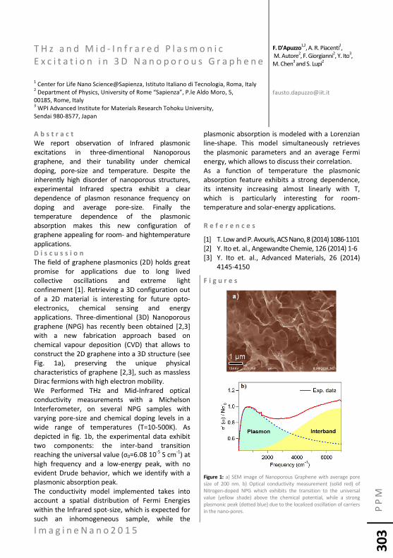
I m a g i n e N a n o 2 0 1 5
PP
M
3
03
T H z a n d M i d - I n f r a r e d P l a s m o n i c E x c i t a t i o n i n 3 D N a n o p o r o u s G r a p h e n e 1 Center for Life Nano Science@Sapienza, Istituto Italiano di Tecnologia, Roma, Italy 2 Department of Physics, University of Rome “Sapienza”, P.le Aldo Moro, 5, 00185, Rome, Italy 3 WPI Advanced Institute for Materials Research Tohoku University, Sendai 980-8577, Japan
A b s t r a c t
We report observation of Infrared plasmonic excitations in three-dimentional Nanoporous graphene, and their tunability under chemical doping, pore-size and temperature. Despite the inherently high disorder of nanoporous structures, experimental Infrared spectra exhibit a clear dependence of plasmon resonance frequency on doping and average pore-size. Finally the temperature dependence of the plasmonic absorption makes this new configuration of graphene appealing for room- and hightemperature applications. D i s c u s s i o n
The field of graphene plasmonics (2D) holds great promise for applications due to long lived collective oscillations and extreme light confinement [1]. Retrieving a 3D configuration out of a 2D material is interesting for future opto-electronics, chemical sensing and energy applications. Three-dimentional (3D) Nanoporous graphene (NPG) has recently been obtained [2,3] with a new fabrication approach based on chemical vapour deposition (CVD) that allows to construct the 2D graphene into a 3D structure (see Fig. 1a), preserving the unique physical characteristics of graphene [2,3], such as massless Dirac fermions with high electron mobility. We Performed THz and Mid-Infrared optical conductivity measurements with a Michelson Interferometer, on several NPG samples with varying pore-size and chemical doping levels in a wide range of temperatures (T=10-500K). As depicted in fig. 1b, the experimental data exhibit two components: the inter-band transition reaching the universal value (σ0=6.08 10-5 S cm-1) at high frequency and a low-energy peak, with no evident Drude behavior, which we identify with a plasmonic absorption peak. The conductivity model implemented takes into account a spatial distribution of Fermi Energies within the Infrared spot-size, which is expected for such an inhomogeneous sample, while the
plasmonic absorption is modeled with a Lorenzian line-shape. This model simultaneously retrieves the plasmonic parameters and an average Fermi energy, which allows to discuss their correlation. As a function of temperature the plasmonic absorption feature exhibits a strong dependence, its intensity increasing almost linearly with T, which is particularly interesting for room-temperature and solar-energy applications.
R e f e r e n c e s
[1] T. Low and P. Avouris, ACS Nano, 8 (2014) 1086-1101 [2] Y. Ito et. al., Angewandte Chemie, 126 (2014) 1-6 [3] Y. Ito et. al., Advanced Materials, 26 (2014)
4145-4150
F i g u r e s
Figure 1: a) SEM image of Nanoporous Graphene with average pore size of 200 nm. b) Optical conductivity measurement (solid red) of Nitrogen-doped NPG which exhibits the transition to the universal value (yellow shade) above the chemical potential, while a strong plasmonic peak (dotted blue) due to the localized oscillation of carriers in the nano-pores.
F. D'Apuzzo1,2, A. R. Piacenti2,
M. Autore2, F. Giorgianni2, Y. Ito3, M. Chen3 and S. Lupi2

I m a g i n e N a n o 2 0 1 5
PP
M
3
04
C o h e r e n t a c o u s t i c e x c i t a t i o n s i n m a g n e t i c s h a p e m e m o r y a l l o y s University Konstanz, Department of Physics, Box M700, 78457 Konstanz, Germany
Excitation with femtosecond laser pulses allow to investigate the elastic properties of new material in the time domain [1]. Here we report on the time-domain investigation of magnetic shape memory alloys [2]. Ferromagnetic Ni-Mn-Ga alloys undergo a martensitic phase transition with little hysteresis, which enables the material to exhibit the shape memory effect. The large interest in applications arising from the large magnetic-field-induced strain in the material has led to intensive research about the microscopic origins of its structural phase transition. The martensitic lattice modulation has recently been described as an adaptive phase, constructed by micro-twinning of tetragonal martensitic unit cells. In contrast, a harmonic modulation and a charge density wave (CDW) ground state were proposed, supported by the observation of phonon anomalies in the austenite phase, the opening of a pseudogap and collective excitations. Here we present ultrafast pump-probe measurements, which are sensitive to both zone-folded acoustic modes in a superstructure and collective excitations in strongly correlated systems.
We observe a mode at THz frequency in the martensite phase, which is strongly influenced by temperature and by the doping with cobalt, implying a strong electron-phonon coupling. The following co-workers contributed to this work: Martin Schubert, Hanjo Schäfer, Jan Mayer, Mike Hettich, Aleksej Laptev, Moritz Merklein, Chuan He, Martin Grossmann, Oliver Ristow, Jure Demsar, Mikhail Fonin, Yuansu Luo, Konrad Samwer, and Vitalyi Gusev.
R e f e r e n c e s
[1] Special issue Ultrafast Acoustics. Edited by E.
Péronne and B. Perrin, Ultrasonics 56, 1-171 (2015). [2] M. Schubert et al., submitted.
F i g u r e s
Figure 1: left: Time domain pump probe traces of NiMnGa shape memory alloy. Right: Extracted oscillations frequencies of NiMnGa and Co-doped NiMnGa for temperatures below the martensite-austenite phase transition temperature.
Thomas Dekorsy

I m a g i n e N a n o 2 0 1 5
PP
M
3
05
P l a s m o n i c s i n a t o m i c a l l y f l a t g o l d s t r u c t u r e s 1 ICFO Institut de Ciències Fotòniques, Mediterranean Technology Park, 08860 Castelldefels (Barcelona), Spain 2 ICREA-Institució Catalana de Recerca i Estudis Avançats, Passeig Lluís Companys 23, 08010 (Barcelona), Spain
Plasmons in atomically thin gold structures have been experimentally observed over the past decade, in particular for atomic gold wires formed at the steps of Si(557) when it is decorated with a low-coverage gold layer [1 - 4]. The observation of plasmons in these systems has been carried out using electron energy-loss spectroscopy, as they are ultra-confined, so that their coupling to light is too weak to be observed. Stimulated by these results, we theoretically study finite-length atomically thin nanowires and nanoribbons. Our purpose is to increase the coupling to light in order to use these structures as atomic-scale plasmonic units. As a first step we revisit experimental data of plasmons in infinitely long atomic gold wires and fit them to both classical and quantum-mechanical models based on the dielectric theory and the random-phase approximation, respectively. These models fit the plasmon dispersion relation extremely well for reasonable choices of parameters. We then calculate absorption cross section of finite nanowires (see Fig. 1). We predict absorptivities of ~5% for arrays of nanorods on the Si(557) surface and ~22% in vacuum. Higher unity-order cross sections are obtained for wires of finite lateral size in the atomic-scale range. Our results pave the way towards the use of atomic-scale gold structures for nanophotonics. R e f e r e n c e s
[1] K. N. Altmann et al., Phys. Rev. B, 64, 035406 (2001). [2] J. N. Crain et al., Phys. Rev. B, 69, 125401 (2004). [3] T. Nagao et al., Phys. Rev. Lett., 97, 116802 (2006). [4] T. Nagao et al., Sci. Technol. Adv. Mater., 11, 054506
(2010).
F i g u r e s
Figure 1: (a) Spectra of the absorption cross section of nanorods of
radius a = 0.1888 nm and different lengths L for light incident with its electric along the rod axis, as obtained from the boundary-element method. (b). Light frequency at the cross section maximum (left vertical axis) and maximum value of the cross section (right axis) for
rods supported on different substrates (characterized by ε) as a function of the ratio between nanorod length and radius.
! ! "! # ! "$ ! "$# ! "% ! "%# ! "&
!
! "#
$
$"#
%
%"#
!'(')%"#*
%&#$!%!&!
#')+, *
$ / $ p
L2a
(a) (b)
! " #" $" %" &""
! '"
"
"(")
"(&
"(&)
"(!
"(! )
"(*
"(! )
"()
"(+)
&
&(! )
&()
,-./#'0!"!1
$/2/&
$/2/!
$/2/&!
$/2/&
$/2/!
$/2/&!
% /
%p
(b)
S. de Vega1and
F. Javier García de Abajo1,2
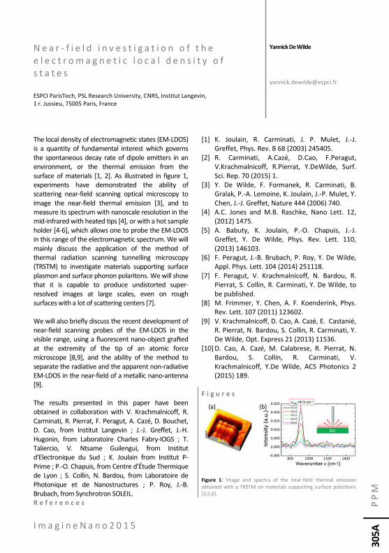
I m a g i n e N a n o 2 0 1 5
PP
M
30
5A
N e a r - f i e l d i n v e s t i g a t i o n o f t h e e l e c t r o m a g n e t i c l o c a l d e n s i t y o f s t a t e s ESPCI ParisTech, PSL Research University, CNRS, Institut Langevin, 1 r. Jussieu, 75005 Paris, France The local density of electromagnetic states (EM-LDOS) is a quantity of fundamental interest which governs the spontaneous decay rate of dipole emitters in an environment, or the thermal emission from the surface of materials [1, 2]. As illustrated in figure 1, experiments have demonstrated the ability of scattering near-field scanning optical microscopy to image the near-field thermal emission [3], and to measure its spectrum with nanoscale resolution in the mid-infrared with heated tips [4], or with a hot sample holder [4-6], which allows one to probe the EM-LDOS in this range of the electromagnetic spectrum. We will mainly discuss the application of the method of thermal radiation scanning tunnelling microscopy (TRSTM) to investigate materials supporting surface plasmon and surface phonon polaritons. We will show that it is capable to produce undistorted super-resolved images at large scales, even on rough surfaces with a lot of scattering centers [7]. We will also briefly discuss the recent development of near-field scanning probes of the EM-LDOS in the visible range, using a fluorescent nano-object grafted at the extremity of the tip of an atomic force microscope [8,9], and the ability of the method to separate the radiative and the apparent non-radiative EM-LDOS in the near-field of a metallic nano-antenna [9]. The results presented in this paper have been obtained in collaboration with V. Krachmalnicoff, R. Carminati, R. Pierrat, F. Peragut, A. Cazé, D. Bouchet, D. Cao, from Institut Langevin ; J.-J. Greffet, J.-H. Hugonin, from Laboratoire Charles Fabry-IOGS ; T. Taliercio, V. Ntsame Guilengui, from Institut d'Electronique du Sud ; K. Joulain from Institut P-Prime ; P.-O. Chapuis, from Centre d’Étude Thermique de Lyon ; S. Collin, N. Bardou, from Laboratoire de Photonique et de Nanostructures ; P. Roy, J.-B. Brubach, from Synchrotron SOLEIL. R e f e r e n c e s
[1] K. Joulain, R. Carminati, J. P. Mulet, J.-J. Greffet, Phys. Rev. B 68 (2003) 245405.
[2] R. Carminati, A.Cazé, D.Cao, F.Peragut, V.Krachmalnicoff, R.Pierrat, Y.DeWilde, Surf. Sci. Rep. 70 (2015) 1.
[3] Y. De Wilde, F. Formanek, R. Carminati, B. Gralak, P.-A. Lemoine, K. Joulain, J.-P. Mulet, Y. Chen, J.-J. Greffet, Nature 444 (2006) 740.
[4] A.C. Jones and M.B. Raschke, Nano Lett. 12, (2012) 1475.
[5] A. Babuty, K. Joulain, P.-O. Chapuis, J.-J. Greffet, Y. De Wilde, Phys. Rev. Lett. 110, (2013) 146103.
[6] F. Peragut, J.-B. Brubach, P. Roy, Y. De Wilde, Appl. Phys. Lett. 104 (2014) 251118.
[7] F. Peragut, V. Krachmalnicoff, N. Bardou, R. Pierrat, S. Collin, R. Carminati, Y. De Wilde, to be published.
[8] M. Frimmer, Y. Chen, A. F. Koenderink, Phys. Rev. Lett. 107 (2011) 123602.
[9] . ra hma ni o , . Cao, . Ca , . Castani , R. Pierrat, N. Bardou, S. Collin, R. Carminati, Y. De Wilde, Opt. Express 21 (2013) 11536.
[10] . Cao, . Ca , M. Calabrese, R. Pierrat, N. Bardou, S. Collin, R. Carminati, V. Krachmalnicoff, Y.De Wilde, ACS Photonics 2 (2015) 189.
F i g u r e s
Figure 1: Image and spectra of the near-field thermal emission obtained with a TRSTM on materials supporting surface polaritons [3,5,6].
Yannick De Wilde

I m a g i n e N a n o 2 0 1 5
PP
M
3
06
H i e r a r c h i c a l n a n o s t r u c t u r e d m a t e r i a l s f o r p h o n o n c o n t r o l a n d t h e r m o e l e c t r i c a p p l i c a t i o n s 1 Max Planck Institute for Polymer Research, Mainz, Germany 2 Universidad do Rio Grande do Norte, Natal, Brazil 3 Cardiff University, School of Chemistry, Cardiff, UK 4 Donostia International Physics Center, San Sebastian, Spain 5 IKERBASQUE: Basque Foundation for Science, Bilbao, Spain
Among the possible routes proposed to design materials with tailored phononic and thermal properties hierarchical nanostructuring displays a vast potential, especially for thermoelectric energy conversion, with unprecedented efficiency ]1]. In fact, introducing different types of phonon scatterers , from the atomic scale to the nano- and meso-scale leads to an effective reduction of the thermal conductivity of materials. Here we propose, by means of atomistic simulations, two different way to exploit the hierarchical nanostructuring, to improve the thermoelectric performance of bulk PbSe and of ultra-thin Silicon membranes. In the case of PbSe we propose an effective way of generating a broad distribution of grains (Fig.1) that scatter phonons over the whole frequency spectrum. For Si membranes, we elucidate the role of dimensionality reduction, alloying and surface nanopatterning [2] in tuning their phonon dispersion relations and thermal conductivity.
For both systems we provide a detailed mechanistic explanation of the effect of nanostructuring on phonon transport, proposing design rules and fabrication processes for enhanced thermoelectric performances. This work is partially supported by the EU, under the FP7-FET-ENERGY project MERGING (Grant No. 309150). R e f e r e n c e s
[1] Biswas, K.; He, J.; Blum, I. D.; Wu, C.-I.; Hogan, T. P.;
Seidman, D. N.; Dravid, V. P.; Kanatzidis, M. G. High-Performance Bulk Thermoelectrics with All-Scale Hierarchical Architectures. Nature 2012, 489, 414–418.
[2] Davis, B. L.; Hussein, M. I. Nanophononic Metamaterial: Thermal Conductivity Reduction by Local Resonance. Phys. Rev. Lett. 2014, 112, 055505.
F i g u r e s
Figure 1: Different scales of grain size distributions in PbSe
S. Neogi1, D. Selli1, C. Mangold1, L.F.C. Pereira2, S. Leoni3, D. Donadio
1,4,5

I m a g i n e N a n o 2 0 1 5
PP
M
3
07
L i g h t E m i t t i n g S e m i c o n d u c t o r N a n o s t r u c t u r e s S t u d i e d b y S N O M 1 NT-MDT Co., 100 Zelenograd, Moscow, 124482 Russia 2 Ioffe Institute, 26 Polytechnicheskaya, Saint Petersburg, 194021 Russia 3 National Research University ITMO, 47 Kronverkskii, Saint Petersburg, 197101 Russia 4 University Notre Dame, Notre Dame, IN 46556 USA
We review our recent SNOM studies on semiconductor laser, quantum dots and quantum microdisks in near-IR spectral region.
The near- and the far-field distributions of propagating light modes from a high-power laser diode were studied by aperture SNOM in XYZ-mapping regime. Diode laser has a line shape 100 µm-aperture and emits in the range 1073-1075 nm. Simple modeling of 3D light emission distribution was also performed and compared with experimental results. The simulated distributions were consistent with the experiment and permitted clarification of the configuration of the transverse modes of the laser. On the emitting facet, in the near-field, an asymmetric distribution of the radiation was revealed, which manifests the mixing of the odd and even (1st and 2nd) modes. 3D light emission distribution measured by SNOM is compared to that measured by a confocal microscope using objectives with different numerical aperture. Resolution and light collection limits of classical confocal microscopy are explicitly demonstrated.
Photoluminescence (PL) of self assembled InP/GaInP quantum dots (QDs) of different sizes from 10 to 200 nm were studied. Illumination-collection regime was used (excitation and emission collection through the same SNOM aperture). Hyperspectral SNOM photoluminescence maps resolving individual QDs could be easily obtained. PL spectra of individual QDs (with emission at 700-780 nm) were measured; spectral differences between QDs of different sizes were studied. Initial fluorescence lifetime imaging SNOM measurements were also performed.
Configuration with far field side excitation under the SNOM cantilever probe and collection through SNOM aperture was applied to investigate whispering-gallery modes distribution in a semiconductor microdisk resonator of 2 µm diameter containing InP/GaInP QDs. Fine structure of optical whispering gallery (circular) and Fabry
Perot (radial) modes were identified both spectrally and spatially. On the image below shown simultaneously obtained topography (a), distribution of selected peak intensity (753-757 nm range) (b) corresponds to a whispering-mode distribution in the resonator. Typical near-field microdisk spectrum is shown on the image (c).
R e f e r e n c e s
[1] A. V. Ankudinov, M. L. Yanul, S. O. Slipchenko, A. V. Shelaev, P. S. Dorozhkin, A. A. Podoskin, and I. S. Tarasov, Optics Express, 22, pp. 26438-26448 (2014)
[2] Y. Chu, A. M. Mintairov, Y. He, J. L. Merz, N. A. Kalyuzhnyy, V. M. Lantratov, S. A. Mintairov, Physics Letters A, 373, 1185 (2009).
F i g u r e s
a) b)
c)
Figure 1: a) Microdisc AFM topography; b) 753-757 nm peak intensity; c) SNOM spectrum of whispering-gallery modes.
A.V. Shelaev1, A.V. Ankudinov2,3, A.M. Mintairov2,4, S.O. Slipchenko2, and P.S. Dorozhkin
1

I m a g i n e N a n o 2 0 1 5
PP
M
3
08
E n g i n e e r i n g l i g h t t r a n s p o r t i n t i t a n i a -d o p e d m u l t i f u n c t i o n a l e l a s t o m e r s 1 Instituto de Ciencia de Materiales de Madrid (ICMM, CSIC), Calle Sor Juana Inés de la Cruz 3, 28049 Madrid, Spain 2 Hospital Nacional de Parapléjicos, Finca de la Peraleda s/n, 45071 Toledo, Spain
Composites incorporating an optically functional phase embedded in polymeric matrices are a platform of choice for the development of optical systems such as flexible, transparency preserving materials with high refractive index [1]. In these cases, the size of the fillers is usually much smaller than light wavelength, so that scattering is minimized. To facilitate the high refractive index, titania nanoparticles are frequently selected [2]. On the other turn, the Mie regime is reached if the size of the particles is of the order of the wavelength, situation in which the scattering is significantly enhanced. Due to multiple scattering [3], light transport on those media becomes diffusive.
Important advances have been realized in the materials community in search for multifunctional features impacting the performance of systems and devices and, in this sense, photonics is not an exception. As an example, we recently reported the possibility of programming the lattice parameter of a two dimensional photonic crystal [4] by making use of multifunctional shape memory polymers [5]. While well-ordered structures are essential in photonic crystals, disordered materials, presenting diffusive transport, may be also extremely interesting [6] and they have proven impact on applications such as random lasers or imaging through opaque media.
In this work [7], we fabricated elastomeric composites by embedding titania particles with an average size of ca. 230 nm in a shape memory polymer belonging to the family of polydiolcitrates. As shown by modulated differential scanning calorimetry, these composites displayed a melting transition in range with previous reports [8], which is responsible for the physical switching mechanism originating the shape memory effect. Depending on the temperature or on the concentration of fillers, the proposed materials may be highly translucent or opaque. The light transport, specifically the transport mean free
path, was characterized using coherent backscattering measurements and shown to depend on the amount of titania incorporated.
The reported composites may find application as a new kind of actuators or as part of novel programmable materials for exploring new avenues in photonics.
Acknowledgements: This work was partially supported by EU FP7 NoE Nanophotonics4Energy grant No. 248855, the Spanish MICINN project MAT2012–31659 (SAMAP), and Comunidad de Madrid S2009/MAT-1756 (PHAMA) program. A.E. was supported by the FPI Ph.D. program from the MICINN. M.C.S. acknowledges Instituto de Salud Carlos III - MINECO for a Miguel Servet contract (CP13-00060).
R e f e r e n c e s
[1] L. Beecroft, C. Ober, Chemistry of Materials, 9
(1997) 1302. [2] A. Chandra, L. Turng, S. Gong, D. C. Hall, D. F.
Caulfield, Polymer Composites, 28 (2007) 241. [3] B. Van Der Mark, M. P. Van Albada, A.
Lagendijk, Physical Review B, 37 (1988) 3575. [4] A. Espinha, M. C. Serrano, A. Blanco, C. López,
Advanced Optical Materials, 2 (2014) 516. [5] M. Behl, M. Razzaq, A. Lendlein, Advanced
Materials, 22 (2010) 3388. [6] D. S. Wiersma, Nature Photonics, 7 (2013) 188. [7] A. Espinha et al. Submitted (2015). [8] M. C. Serrano, L. Carbajal, G. Ameer, Advanced
Materials, 23 (2011) 2211.
André Espinha1,
María Concepción Serrano2, Álvaro Blanco1, Cefe López1

I m a g i n e N a n o 2 0 1 5
PP
M
3
09
R a d i a t i v e h e a t t r a n s f e r t h r o u g h n a n o m e t e r - s i z e g a p s 1 Departamento de Física Teórica de la Materia Condensada and Condensed Matter Physics Center (IFIMAC), Universidad Autónoma de Madrid, Madrid, 28049, Spain 2 Department of Mechanical Engineering, University of Michigan, Ann Arbor, USA
One of the central open problems in nanoscience is the study of the heat transport in nanoscale devices, which has remained largely unexplored due to experimental challenges. In this context, a key issue is the understanding of the heat transfer via thermal radiation between systems separated by nanometer-size gaps. In this extreme regime, the electromagnetic near-field is expected to give rise to a dramatic enhancement of the radiative heat transfer, something that has only be quantitatively verified for gaps on the order of 20-30 nm [1]. In this work, we present a combined experimental and theoretical study of the radiative heat transfer in the extreme near-field regime (gaps of 1-10 nm). From the experimental side, we performed systematic studies using AFM-based scanning probes with integrated nanoscale thermocouples [2], which were coated with dielectrics (SiO2 or SiNx). Our experiments of heat transport between the scanning probes and a flat substrate coated with dielectrics, performed in an ultra-high vacuum environment, confirm that heat transport is dramatically enhanced in the near-field. To understand our experimental results, we investigated these near-field enhancements within the framework of the theory of fluctuational electrodynamics [3]. To be precise, we performed extensive numerical simulations making use of a combination of a fluctuating-surface-current formulation of radiative heat transfer with the boundary element method [4,5]. Such a combination allows us describing realistic geometries for our tip-sample setups. Our theoretical results are in good agreement with the measured heat flows between both dielectric and metallic surfaces, which establishes the validity of fluctuational electrodynamics in modeling near-field heat transport all the way to nanometer-size separations.
R e f e r e n c e s
[1] S. Basu, Z. M. Zhang, and C. J. Fu, Int. J. Energy Res. 33 (2009) 1203.
[2] W. Lee, K. Kim, W. Jeong, L.A. Zotti, F. Pauly, J.C. Cuevas, and P. Reddy, Nature 498 (2013) 209.
[3] K. Joulain, J.P. Mullet, F. Marquier, R. Carminati, and J.J. Greffet, Surf. Sci. Rep. 57 (2005) 59.
[4] A. W. Rodriguez, M. T. H. Reid, and S. G. Johnson, Phys. Rev. B 86 (2012) 220302(R).
[5] A. W. Rodriguez, M. T. H. Reid, and S. G. Johnson, Phys. Rev. B 88 (2013) 054305.
F i g u r e s
a
b
Figure 1: a Schematic diagram of the experimental setup. The AFM probes incorporate a thermocouple, made by a spherical Au/Cr junction with a diameter of 200 nm. b Numerical simulation of the spatially resolved heat transfer between a tip and a plate made of silica and separated by a distance of 1 nm. The radius of the tip is 225 nm. The color scale is logarithmic, showing the radiative heat transfer enhancement in the extreme near-field.
V. Fernández Hurtado1, K. Kim2,
B. Song2, W. Lee2, W. Jeong2, J. Feist1, F. J. Garcia-Vidal1, J. C. Cuevas1, E. Meyhofer2 and P. Reddy2
I m a g i n e N a n o 2 0 1 5
PP
M
3
10
P l a s m o n s i n n a n o g r a p h e n e a n d o t h e r a t o m i c s c a l e s y s t e m s ICFO-The Institute of Photonic Sciences Mediterranean Technology Park 08860 Castelldefels (Barcelona), Spain We will review recent advances in the control and understanding of plasmons in systems that have atomic dimensions along one or more directions. In particular, we will discuss plasmons in graphene, carbon nanotubes, and fullerenes, as well as thin metal layers and molecules such as polycyclic aromatic hydrocarbons. A simple, powerful, analytical eigenmode expansion formalism will be reviewed in the electrostatic limit, along with tutorial examples of application to the understanding of plasmons in these systems, including the derivation of approximate expressions for the plasmon frequencies and wave functions. Intrinsic advantages of plasmons in atomic-scale systems will be also discussed, and in particular, their large electrical tunability, their strong nonlinear response, and the possibility of reaching quantum strong coupling.
F. Javier García de Abajo
I m a g i n e N a n o 2 0 1 5
PP
M
3
11
M a g n e t o - o p t i c a l a c t i v i t y i n i n t e r a c t i n g m a g n e t o p l a s m o n i c n a n o d i s k s 1 IMM-Instituto de Microelectrónica de Madrid (CNM-CSIC), Tres Cantos, Madrid, Spain 2 Departamento de Física de la Materia Condensada, UAM, Madrid, Spain 3 Instituto de Estructura de la Materia, CSIC, Madrid, Spain
Metal-dielectric plasmonic nanodisks show a rich optical behaviour with the appearance of two modes of magnetic and electric dipolar character due to the interaction between the disks. These modes couple to the incident light in a different way, giving rise to regions with low and high optical extinction, respectively. Moreover, the insertion of a ferromagnetic component inside the structure introduces magneto-optical activity in the system[1]. As a consequence, metal-dielectric magnetoplasmonic nanodisks exhibit a rich optical and MO spectral phenomenology. It has previously been shown that, in Au/Co/Au nanodisks where a SiO2 layer is inserted, it is possible to obtain nanodisk configurations for which low optical absorption and large MO activity occur at the same spectral range. This is basically achieved by an adequate positioning of the dielectric component within the structure [2]. Here we present our study on the influence that the dielectric spacer thickness has on the interaction between the disks, and as a consequence, on the optical and MO properties of such structures [3,4]. The structures consist of a pure Au nanodisk separated by a SiO2 spacer from a MO component constituted by a 4nmAu/2nmCo multilayer nanodisk, which exhibits perpendicular magnetic anisotropy, reducing the required magnetic field to achieve saturation in polar configuration. It will be shown that these structures exhibit the expected magnetic and electric dipolar modes, both in the optical and MO spectra. The position of the magnetic-like mode strongly depends on the SiO2 thickness, while that of the electric like one remains basically unaltered. As the SiO2 thickness is increased, the strength of the MO activity of the magnetic-like dipolar mode increases much more strongly than the corresponding extinction peak. On the other hand, the MO activity of the electric-like mode decreases
as the SiO2 thickness increases, while the corresponding extinction peak remains nearly unaffected. R e f e r e n c e s
[1] G. Armelles, et al., Adv. Opt. Mat. 1, 10 (2013). [2] J.C. Banthí et al., Adv. Mater. 24, OP36 (2012). [3] G. Armelles, et al., Optics Express 21, 27356 (2013). [4] N. de Sousa et al., Phys. Rev. B 89, 205419 (2014).
Gaspar Armelles1, Alfonso Cebollada1, Fernando García1, María Ujué González1, David Meneses1, Nuno de Sousa2, Luis S. Froufe-Pérez3 and Antonio García-Martín
1
I m a g i n e N a n o 2 0 1 5
PP
M
3
12
T o w a r d s S u b - 1 0 n m N a n o f a b r i c a t i o n o f P l a s m o n i c a n d G r a p h e n e D e v i c e s u s i n g M u l t i p l e E l e c t r o n a n d I o n B e a m s Carl Zeiss Microscopy, Carl Zeiss Str. 56, Oberkochen, Germany Direct write focused ion beam (FIB) machining represents the quickest, most flexible method to fabricate nano-devices for prototyping and research applications. The use of a FIB combined with SEM allows for immediate inspection and refinement steps in the patterning, assuring the desired fidelity. This technology has thus found wide-spread use in fields such as photonics, nano-fluidics, TEM sample preparation, integrated circuit modification, and MEMS. Conventional gallium FIB based on the liquid metal ion source (LMIS) has many notable drawbacks which include the lower limit for feature sizes that can be achieved and Ga implantation. As an illustrative example of machining over multiple length scales, we show here an example of a double bowtie plasmonic device, inspired by the work of Zhang [1] and co-workers. The device consists of four equilateral triangles patterned into 17 nm thick Au films by electron beam lithography. These elements face into one another giving a shape like two crossed bowties. The dimensions of the device are critical to determine the resonant wavelength. The requirements are that the triangles have a side length of approximately 85 nm, with a radius of curvature of 10 nm at the vertices, and a gap between the points of the triangles of about 30 nm. The gaps are varied to alter the plasmonic response of the device. To date, lithographic methods are necessary to form such small objects since traditional Ga FIB does not have the requisite machining precision. The Carl Zeiss ORION NanoFab allows these devices to be made by direct write using three different ion species and completely obviating the need for lithographic processing. The critical dimension can in fact be reduced even further. A three step approach was used to fabricate a double bowtie structure in a 100 nm thick gold film on a glass substrate2. During the first step, Ga FIB is used to open up a 1 µm square window into the film, while leaving behind a square island 200 nm wide in the center as shown in Figure 1. Gallium was used for this first step because it has a sputtering yield 120X higher than He and 4X
higher than Ne (30 keV; as predicted by TRIM3 [2] simulations). The Ga FIB is also capable of higher total beam current for faster material removal of larger volumes. The second step consisted of using the neon beam in the gas field ion source to machine slits in the island which form a cross as demonstrated in Figure 2. Sputtering with Ne avoids Ga contamination into the critical area around the bowtie, yet still provides a 30x speed advantage over helium milling. The sidewall angle of the created features is 82⁰, but this could be improved with trimming by helium, which has shown, in the work by Scipioni et al.43 with sidewall angles of 88⁰. Finally, helium ion milling is utilized to separate the four triangular elements as represented in Figure 3. A top-down view of the completed device is presented in Figure 4. The active area of the device had never been exposed to the Ga beam. The fact that the results can be inspected immediately in-situ, using helium ion microscopy (HIM), also provides the quick feedback and process control that traditional FIB-SEM affords. Extremely tight dimensions can be maintained in the most critical area. Figure 5 shows the center of the bowtie structure. The image has been filtered to highlight the edges for measurement purposes. (We do note a small amount of residual material in the gap). The distance between the triangle vertices is 10 nm (line drawn on image), and the radius of curvature of the vertices is also 5 nm (circle drawn on image). R e f e r e n c e s
[1] Z. Zhang, et al., Nano Letters, 9, 4505 (2009) [2] J Notte, “Charged Particle Microscopy: Why Mass
Matters”, Microscopy Today, 20(5), 16-22 (2012). [3] http://www.srim.org/ [4] Larry Scipioni, et al., J. Vac. Sci. Technol. B 28(6),
C6P18 (2010)
Peter Gnauck

I m a g i n e N a n o 2 0 1 5
PP
M
3
13
F i g u r e s
Figure 1: A 200 nm island of 100 nm thick Au on glass created by Ga FIB milling. Helium ion imaging.
Figure 2: Machining of island with neon beam to form arms of double bow tie structure. Helium ion imaging
Figure 4: Top down image of final device. Helium ion imaging.
Figure 5: Edge-enhanced HIM image of center 100 nm area of double bow tie structure. Line drawn on image is 10 nm. Circle has radius of 5 nm.
I m a g i n e N a n o 2 0 1 5
PP
M
3
14
F i n e t u n i n g o f t h e e m i s s i o n p r o p e r t i e s o f n a n o - e m i t t e r s i n m u l t i l a y e r e d s t r u c t u r e s b y d e t e r m i n i s t i c c o n t r o l o f t h e i r l o c a l p h o t o n i c e n v i r o n m e n t Multifunctional Optical Materials Group. Instituto de Ciencia de Materiales de Sevilla. Consejo Superior de Investigaciones Científicas-Universidad de Sevilla. Sevilla, Spain Porous nanostructured photonic materials in the shape of periodic multilayers have demonstrated their potential in different fields ranging from photovoltaics[1] to sensing[2]. On the one hand their porosity makes it feasible to infiltrate them with an electrolyte or a polymeric matrix (which allows their use in dye sensitized solar cells or as flexible films[3]). On the other, the possibility of controlling their refractive index profile via their porosity or the choice of materials, strongly affects the way light is transported or generated within them. When applications dealing with light absorption or emission are considered, knowledge on how the local density of states (LDOS) is distributed within them is mandatory[4] in order to realize a judicious design which maximizes light matter interaction. In order to do so, access to a photonic probe which senses the LDOS at different spatial positions is desired. Such probe must have reduced dimensions (in order to achieve a high spatial resolution in the mapping of the LDOS) and should lend itself to be incorporated in the fabrication procedure in such a manner that its spatial position within the sample can be controlled. In this work we report a detailed study of how dye doped polystyrene nanospheres constitute an effective LDOS probe to study its distribution within nanostructured photonic media. Nanospheres with a diameter of 25 nm are incorporated in the fabrication procedure of nanostructured photonic multilayers (through a combination of spin and dip-coating with suspensions of oxide nanoparticles) in such a way that the high optical quality of the fabricated structure is maintained. Introducing the polymeric spheres at different stages of the fabrication process allows placing them at several positions of the structured sample. A combined use of photoluminescence spectroscopy and time resolved measurements are used to optically characterize the samples. While the former shows
how depending on the probe position its PL intensity can be enhanced or suppressed, the latter allows to probe the LDOS changes within the sample, monitored via changes in its lifetime. We demonstrate how information on the local photonic environment can be retrieved with a spatial resolution of 25 nm (provided by the probe size) and relative changes in the decay rates as small as ca. 1%, evidencing the possibility of exerting a fine deterministic control on the photonic surroundings of an emitter. R e f e r e n c e s
[1] C. López-López, S. Colodrero, M. E. Calvo and H. Míguez, Energy Environ. Sci., 23 (2013), 2805.
[2] A. Jiménez-Solano, C. López-López, O. Sánchez-Sobrado, J. M. Luque, M. E. Calvo, C. Fernández-López, A. Sánchez-Iglesias, L. M. Liz-Marzán and H. Míguez. Langmuir, 28 (2012), 9161.
[3] J. R. Castro-Smirnov, M. E. Calvo and H. Míguez, Adv. Funct.Mater, 23, (2013), 2805.
[4] N. Danz, R. Waldhäusl, A. Bräuer and R. Kowarschik, J. Opt. Soc. Am. B, 19 (2010), 412.
F i g u r e s
Alberto Jiménez-Solano, Juan F. Galisteo-López and Hernán Míguez

I m a g i n e N a n o 2 0 1 5
PP
M
3
15
N a n o c r y s t a l l i n e D i a m o n d E l e c t r o d e f o r D y e - S e n s i t i z e d S o l a r C e l l s 1 J. Heyrovský Institute of Physical Chemistry, v.v.i., Academy of Sciences of the Czech Republic, Prague, Czech Republic 2 Institute of Physics, v.v.i., Academy of Sciences of the Czech Republic, Prague, Czech Republic 3 Institute of Organic Chemistry and Biochemistry, v.v.i. Academy of Sciences of the Czech Republic, Prague , Czech Republic. 4 IMEC, IMOMEC Division, University Campus Hasselt, Diepenbeek, Belgium The B-doped nanocrystalline diamond (BDD) can be considered as a promising alternative of p-NiO in photocathode in dye-sensitized solar cells (DSCs). Diamond films are attractive by their excellent chemical and electrochemically stability, optical transparency and favorable electrical properties. The electrochemical inertness of BDD is beneficial in view of the corrosive nature of certain electrolyte solutions used in DSCs. Nanocrystalline boron doped diamond films were grown by a microwave plasma enhanced chemical vapor deposition.[1,2] Electrochemical impedance spectroscopy provided the flatband potentials and concentrations of acceptors, which relate to the B-concentrations from the neutron depth profiling. Electrochemical cleaning of the surface from sp2 carbon impurities was demonstrated by Raman spectroscopy.[1] Spectral sensitization of the nanodiamond surface was carried out by anchoring of dyes like 4-(bis-4-[5-(2,2-dicyano-vinyl)-thiophene-2-yl]-phenyl-amino)-benzoic acid (P1 from Dyenamo AB). In a two-step procedure, polyethyleneimine is adsorbed on hydrogenated diamond surface and subsequently modified with P1. The sensitized diamond exhibits stable cathodic photocurrents under visible light illumination in aqueous electrolyte solution with dimethylviologen serving as electron mediator.[3] In spite of the simplicity of the surface sensitization protocol, the photoelectrochemical performance is similar or better compared to that of other sensitized diamond electrodes which were reported in previous studies (2008-14).[4] Acknowledgment. This work was supported by the Grant Agency of the Czech Republic (contract No. 13-31783S).
R e f e r e n c e s
[1] Z. Vlckova-Zivcova, O. Frank, V. Petrak et al., Electrochim.Acta 18, 518 (2013).
[2] P. Ascheulov, J. Sebera, A. Kovalenko et al., Eur.Phys.J.B 86, 443 (2013).
[3] H. Krysova, Z. Vlckova-Zivcova, J. Barton et al., Phys.Chem.Chem.Phys. DOI: 10.1039/C4CP04148H, (2014).
[4] S. W. Yeap, D. Bevk, X. Liu et al., RCS Adv. 4, 42044 (2014).
F i g u r e s
L. Kavan1; Z. Vlckova-Zivcova1; H.
Krysova1; V. Petrak2; J. Barton3; P. Cigler3; M. Nesladek4

I m a g i n e N a n o 2 0 1 5
PP
M
3
16
M a g n e t o p l a s m o n i c d e s i g n r u l e s f o r a c t i v e m a g n e t o - o p t i c s 1 Chalmers University of Technology, 41296 Gothenburg, Sweden 2 CIC nanoGUNE Consolider, 20018 Donostia-San Sebastian, Spain 3 K.N. Toosi University of Technology, Tehran 16314, Iran 4 University of Gothenburg, 41296 Gothenburg, Sweden 5 IKERBASQUE, Basque Foundation for Science, 48011, Bilbao, Spain Magnetoplasmonics offers a versatile smart toolbox in the quest for actively tunable metasurfaces. Here we present design rules for metasurfaces based on magnetoplasmonic nanoantennas that allow for advanced control of light polarization states. Magneto-optical materials are often used to control the polarization state of propagating waves in integrated optical circuits. The polarization control originates from the off-diagonal terms in the dielectric tensor of these materials that can be activated by applying an external magnetic field. This gives rise to tunable non-reciprocal propagation of the light waves, an effect that has been intensively studied in optical insulators. Similar effects can be obtained in magnetoplasmonic nanoantennas, where the localized near-field enhancement at the plasmon resonance amplifies the intrinsic magneto-optical effects and allows tailoring it by means of the nanoantenna design. Here we derive simple design rules that can be exploited for fully 3D magnetoplasmonic nanoantennas in order to obtain magnetically tunable active metasurfaces. We investigated the magnetoplasmonic response of 2D and 3D nanoantennas in all three conventional magneto-optical Kerr effect (MOKE) geometries, namely longitudinal (L), polar (P) and transversal (T). In the former two cases, the polarization state of a transmitted wave is changed, resulting in a Kerr rotation and ellipticity, while in the latter case the intensity is modulated by the applied magnetic field. In figure 1 we illustrate the broadband tunability of the Kerr response for different orientations of elliptical nanoantennas that support three mutually orthogonal plasmon modes. The magnitude of the modulation and its sign can be predicted based on the polarizabilities of the nanostructures along their different symmetry axes, as illustrated by the formulas 1-3.
For the selected case (incident angle 25°) we can observe how the magnitude of the Kerr signal scales according to the design rules in equation 1-3. Irrespective of the Kerr configuration, the largest signals are obtained when two plasmon modes in the numerator exhibit a simultaneous resonant behaviour (see vectors in a, black and red lines in panel b, equations 1). For non-perpendicular incidence, two plasmon modes are directly excited by the incident wave (αxx and αzz), while the third one can be activated through the spin-orbit interaction (αyy) for the L- and P-configurations. In the T-MOKE case both the directly excited plasmon modes (αxx and αzz) are coupled by the spin-orbit interaction, allowing unprecedented and versatile H-modulated control of the light intensity. R e f e r e n c e s
[1] N. Maccaferri et al., Opt. Express 21, (2013) 9875-9889
[2] K. Lodewijks, N. Maccaferri et al., Nano Lett. 14 (2014), DOI: 10.1021/nl504166n
Kristof Lodewijks1, Nicolò
Maccaferri2, Tavakol Pakizeh3, Randy K. Dumas4, Irina Zubritskaya1, Johan Åkerman4, Paolo Vavassori2,5, Alexandre Dmitriev1
[email protected] www.kristoflodewijks.be

I m a g i n e N a n o 2 0 1 5
PP
M
3
17
F i g u r e s
L-MOKE ∝αSOαyyαzz sinγ
αxx cos2γ +αzzsin
2γ
(1)
P-MOKE ∝αSOαyyαxx cosγ
αxx cos2 γ +αzz sin
2 γ
(2)
T-MOKE ∝αzz
αxx
tanγtanγ +αSOαxx
1+αSOαzz tanγ
(3)
Figure 1: Calculated MOKE signals [1, 2] for p-polarized light in different 3D nanoellipses (a) and different Kerr geometries. (b) Longitudinal, (c) Polar and (d) Transversal. Equations 1-3 show the scaling of MOKE signals for the respective geometries with the polarizabilities along the symmetry axes of the nanoantennas and the incident angle γ

I m a g i n e N a n o 2 0 1 5
PP
M
3
18
1 D L i n e C u r r e n t M o d e l f o r P l a s m o n i c H a l f - W a v e A n t e n n a s : F r o m N a n o r o d s t o N a n o c a r r o t s 1 Universidad de Zaragoza, EINA, María de Luna 3, 50018 Zaragoza, Spain 2 Data Storage Institute (A-STAR), 5 Engineering Drive I, 117608, Singapore 3 Instituto de Estructura de la Materia (IEM-CSIC), Serrano 121, 28006 Madrid, Spain Metallic nanorods constitute the plasmonic analogue to classical half-wave dipole antennas. These structures show spectral lines of distinctly different shapes in their optical extinction cross-section under near-normal plane wave illumination that are originated by the interaction of longitudinal surface plasmon resonances. In our previous works [1, 2], we have shown that plasmon resonances of odd mode parity present Fano interference in the scattering cross-section, resulting in asymmetric spectral lines. Contrarily, modes with even parity appear as symmetric Lorentzian lines. In order to describe the emergence of either constructive or destructive mode interference, we also proposed a semi-analytical 1D line current model that directly explains the mode-parity dependence of the Fano-like interference. Now, we extend our model to nanorods with variable geometrical cross-section so that it enables us to describe the optical response of recently reported asymmetric silver "nanocarrot" structures [3].
R e f e r e n c e s
[1] F. López-Tejeira et al., New Journal of Physics, 14 (2012) 023035.
[2] N. Verellen et al., Nano Letters, 14 (2014) 2322. [3] H. Liang et al., Journal of the American Chemical
Society,135 (2013) 9616.
F. López-Tejeira1, R. Paniagua-
Domínguez2 and J.A. Sánchez-Gil3
I m a g i n e N a n o 2 0 1 5
PP
M
3
19
L o w t e m p e r a t u r e t h e r m a l p r o p e r t i e s o f t w o - d i m e n s i o n a l p h o n o n i c c r y s t a l s Nanoscience Center, Department of Physics, P.O. Box 35, University of Jyväskylä, FI-40014, Finland Controlling thermal properties in the nanoscale has become more and more relevant in recent years, in light of the strong push to develop novel energy harvesting techniques based on thermoelectricity, the need to improve the heat dissipation out of semiconductor devices, and the push to increase the sensitivity of bolometric radiation detectors [1]. A lot of research has lately focused on lowering phonon thermal conductivity using nanoscale structuring of materials to increase scattering. On the other hand, much less attention has been given to controlling phonon thermal conductance by engineering the phonon dispersion relations, in other words the phonon ‘band structure’. Dispersion relations determine both the group velocity and the density of states, and therefore directly influence thermal conduction. Many of the phonons involved in thermal conduction actually have wavelengths much larger than the atomic lattice constant [1], and thus, by structuring material at some longer length scale, phonons with wavelengths around that length will undergo strong coherent Bragg interference. If this extra structuring is periodic, the devices are called phononic crystals [2], with strongly modified band structure, density of states and group velocity for long wavelength phonons. This modification is expected to be extremely strong in the low-temperature limit, where thermal wavelengths can be of the order of 1 µm and where incoherent phonon-phonon and phonon-impurity scattering is negligible. Here, we discuss this line of approach for controlling thermal conduction [3] and present our recent experimental and computational studies in two-dimensional phononic crystals (PnCs) at sub-Kelvin temperatures. A typical sample consists of a periodic array of holes etched into a 0.5 µm thick silicon nitride membrane. We compared the results of two PnCs with different periodicities to an uncut membrane sample and observed a strong reduction of thermal conductance up to a factor of 30, with a concurrent change in the temperature dependence, agreeing quantitatively with our numerical
computation based on finite element method (FEM) simulations of the modified dispersion relations of the PnC devices. As our calculation of the thermal conduction was performed in the fully ballistic limit, we draw the conclusion that coherent, interference-based phonon band structure modification is behind the observations and thus phonon thermal conduction can be controlled by using the wave-properties of phonons, instead of just the particle (scattering) properties. R e f e r e n c e s
[1] I. J. Maasilta and A. Minnich, Phys. Today 67, 285-290 (2014)
[2] Y. Pennec, J. O.Vasseur, B. Djafari-Rouhani, L. Dobrzynski, P. Deymier, Surf. Sci. Rep. 65, 229–291 (2010).
[3] N. Zen, T. A. Puurtinen, T. J. Isotalo, S. Chaudhuri, and I. J. Maasilta, Nat. Commun. 5, 3435 (2014).
I. J. Maasilta

I m a g i n e N a n o 2 0 1 5
PP
M
3
20
S y n t h e s i s a n d m e a s u r e m e n t o f p o l a r i z a t i o n s t a t e s w i t h s i l i c o n n a n o a n t e n n a s 1 Nanophotonics Technology Center, Universitat Politècnica de València, Camino de Vera s/n, 46022, Valencia, Spain 2 Department of Physics, King’s College London, Strand, London WC2R 2LS, UK
It has been recently shown that the polarization of the source exciting a guided wave via near-field coupling plays a key role in determining the propagation direction of the guided way. This way, point dipoles exhibiting circularly polarization are converted into guided waves so that opposite excitation spins result in counter-propagating guided waves. This powerful concept, firstly demonstrated in plasmonics for visible light [1], can also be applied to other wavelengths and photonic platforms. For instance, it can be implemented in a silicon photonics integrated platform working at telecom wavelengths by inserting a dielectric scatterer (or nanoantenna), which performs as the exciting element, placed in the close proximity of a silicon waveguide. In [2], we used such a concept to demonstrate experimentally at telecom wavelengths that a silicon microdisk nanoantenna can resolve the handedness (or spin) of a circularly polarized light beam (see Fig. 1(a)). If a rectangular nanoantenna is employed (see Fig. 1(b)), linearly polarized photons will be directed towards one side or the waveguide or the opposite one depending on its polarization angle. This enables sorting linearly polarized photons with ideally infinite contrast ratio in a very simple way and with an extremely compact structure [3]. By reciprocity, the silicon nanoantenna-waveguide can also be used to radiate photons with a tailored polarization. This way, in [2] we demonstrated the ability of radiating circularly polarized photons by the microdisk nanoantenna, being the handedness determined by the choice of the feeding waveguide. More importantly, by feeding the nanoantenna simultaneously by its both sides, it becomes feasible to generate compound polarization states [4]. This way, we have demonstrated theoretically and experimentally that any polarization state on the Poincaré sphere can be generated from a single nanoantenna [4]. Finally, by properly combining the different nanoantennas, it is possible to detect the (this is, all the Stokes parameters) in a single measurements. This would lead to a very compact integrated photonic circuit that could dynamically
determine the complete polarization state of an impinging plane wave, which could find application in polarimetry, spectrometry or high-speed optical communications.
R e f e r e n c e s
[1] F. J. Rodríguez-Fortuño et al., 340 (2013), 328. [2] F. Rodríguez-Fortuño et al., ACS Photonics 1 (2014), 762. [3] F. J. Rodríguez-Fortuño et al., Opt. Lett. 39
(2014), 1394. [4] F. J. Rodríguez-Fortuño et al., Laser Photonics Rev. 8
(2014), L27–L31. F i g u r e s
(a)
(b) (c)
Figure 1: Silicon nanoantennas for managing polarization. (a) A silicon microdisk coupled to two waveguides sorts opposite spins of an incoming wave into opposite waveguides; (b) A rectangular silicon nanoantenna can be used to sort linearly polarized photons; (c) By feeding the nanoantenna by its both sides, the polarization of the emitted light can be properly tailored.
Alejandro Martínez1, Alba
Espinosa-Soria1, Sara Mas1, Amadeu Griol1, Francisco J. Rodríguez Fortuño2
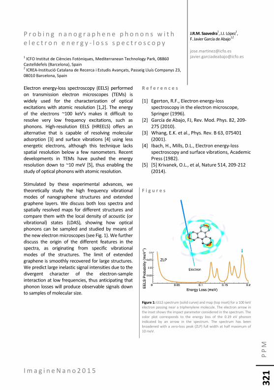
I m a g i n e N a n o 2 0 1 5
PP
M
3
21
P r o b i n g n a n o g r a p h e n e p h o n o n s w i t h e l e c t r o n e n e r g y - l o s s s p e c t r o s c o p y 1 ICFO Institut de Ciències Fotòniques, Mediterranean Technology Park, 08860 Castelldefels (Barcelona), Spain 2 ICREA-Institució Catalana de Recerca i Estudis Avançats, Passeig Lluís Companys 23, 08010 Barcelona, Spain
Electron energy-loss spectroscopy (EELS) performed on transmission electron microscopes (TEMs) is widely used for the characterization of optical excitations with atomic resolution [1,2]. The energy of the electrons ~100 keV's makes it difficult to resolve very low frequency excitations, such as phonons. High-resolution EELS (HREELS) offers an alternative that is capable of resolving molecular adsorption [3] and surface vibrations [4] using less energetic electrons, although this technique lacks spatial resolution below a few nanometers. Recent developments in TEMs have pushed the energy resolution down to ~10 meV [5], thus enabling the study of optical phonons with atomic resolution. Stimulated by these experimental advances, we theoretically study the high frequency vibrational modes of nanographene structures and extended graphene layers. We discuss both loss spectra and spatially resolved maps for different structures and compare them with the local density of acoustic (or vibrational) states (LDAS), showing how optical phonons can be sampled and studied by means of the new electron microscopes (see Fig. 1). We further discuss the origin of the different features in the spectra, as originating from specific vibrational modes of the structures. The limit of extended graphene is smoothly recovered for large structures. We predict large inelastic signal intensities due to the divergent character of the electron-sample interaction at low frequencies, thus anticipating that phonon losses will produce observable signals down to samples of molecular size.
R e f e r e n c e s
[1] Egerton, R.F., Electron energy-loss
spectroscopy in the electron microscope, Springer (1996).
[2] García de Abajo, FJ, Rev. Mod. Phys. 82, 209-275 (2010).
[3] Whang, E.K. et al., Phys. Rev. B 63, 075401 (2001).
[4] Ibach, H., Mills, D.L., Electron energy-loss spectroscopy and surface vibrations, Academic Press (1982).
[5] [5] Krivanek, O.L., et al, Nature 514, 209-212 (2014).
F i g u r e s
Figure 1: EELS spectrum (solid curve) and map (top inset) for a 100 keV electron passing near a triphenylene molecule. The electron arrow in the inset shows the impact parameter considered in the spectrum. The color plot corresponds to the energy loss of the 0.19 eV phonon indicated by an arrow in the spectrum. The spectrum has been broadened with a zero-loss peak (ZLP) full width at half maximum of 10 meV.
J.R.M. Saavedra1, J.J. López1,
F. Javier García de Abajo1,2
I m a g i n e N a n o 2 0 1 5
PP
M
3
22
E n g i n e e r i n g e l e c t r i c a l w i r e s i n h o n e y c o m b l a t t i c e s Theory and Simulation of Materials (THEOS) and National Center for Computational Design and Discovery of Novel Materials (MARVEL) Ecole Polytechnique Federale de Lausanne, Switzerland Unprecedented and fascinating phenomena have been recently observed at oxide interfaces between centrosymmetric cubic materials, where polar discontinuities can give rise to polarization charges and electric fields that drive a metal-insulator transition and the appearance of a two-dimensional electron gas. Lower dimensional analogues are possible, and honeycomb lattices offer a fertile playground thanks to their versatility and the extensive on-going experimental efforts in graphene and related materials. Here we suggest different realistic pathways to engineer polar discontinuities in honeycomb lattices, and support these su gestions with extensive first-principles calculations. Several approaches are dis- cussed, based on (i) nanoribbons, where a polar discontinuity against the vacuum emerges, and (ii) functionalizations, where covalent ligands are used to engineer polar discontinuities by selective or total functionalization of the parent systems. All the cases considered have the potential to deliver innovative applications in ultra-thin and flexible solar-energy devices and in micro- and nano-electronics.
Marco Gibertini, Giovanni Pizzi, and Nicola Marzari

I m a g i n e N a n o 2 0 1 5
PP
M
3
23
F a s t f a b r i c a t i o n o f p h o t o n i c g l a s s e s a c h i e v e d b y p r e s s u r e Instituto de Ciencia de Materiales de Madrid ICMM-CSIC c/Sor Juana Inés de la Cruz, 3, Cantoblanco, 28049 Madrid, Spain Photonic random structures presenting multiple light scattering have been of great interest in the last few years [1] and their fabrication has led to the development of new and sophisticated fabrication methods. In these systems, important fundamental phenomena such as Anderson localization of light might take place [2]. Further, polymeric photonic glasses have recently demonstrated resonant light transport [3] in which random lasing can be controlled [4]. Here we show a new method to prepare photonic glasses from different colloidal suspensions (SiO2, Polystyrene, or PMMA) in a very fast way. Starting from raw materials in powder form (as synthesized or purchased) we propose a method for fabricating high quality photonic glasses in minutes, by applying pressure [5]. Our studies on how monodisperse building blocks pack open a new window to understand light behavior in complex optical media. Further, this work might provide deeper knowledge on random granular media at the nanoscale [6]. R e f e r e n c e s
[1] D. S. Wiersma, Nat. Phot. 7 (2013) 188. [2] D. S. Wiersma, P. Bartolini, A. Lagendijk, and R.
Righini, Nat. Phot. 390 (1997) 671–673. [3] P. D. García, R. Sapienza, Á. Blanco, and C.
López, Adv. Mater. 19 (2007) 2597. [4] S. Gottardo, R. Sapienza, P.D. García, Á.
Blanco, D. S. Wiersma, and C. López, Nat. Phot. 2 (2008) 429.
[5] D. Montesdeoca et al. submitted (2015). [6] Y.Kallus, S. Torquato, Ph. Rev. E, 90 (2014)
022114.
F i g u r e s
Figure 1: Resonant total transmission for silica photonic glasses composed of spheres with 920 nm in diameter, for different applied pressures (up). Scanning electron microscopy images and optical image of a silica photonic glass for an applied pressure of 6t (460 MPa) (bottom).
Denise Montesdeoca, Andre Espinha, F. Bayat, Carlos Pecharroman, Cefe Lopez, and Alvaro Blanco
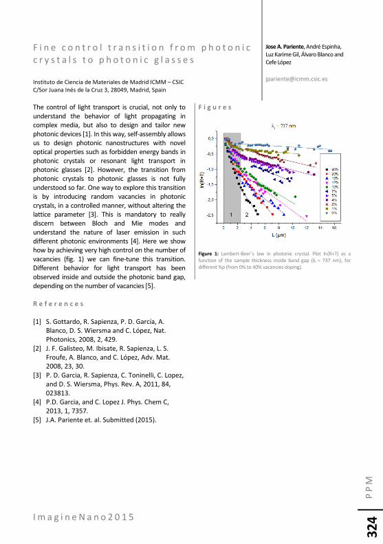
I m a g i n e N a n o 2 0 1 5
PP
M
3
24
F i n e c o n t r o l t r a n s i t i o n f r o m p h o t o n i c c r y s t a l s t o p h o t o n i c g l a s s e s Instituto de Ciencia de Materiales de Madrid ICMM – CSIC C/Sor Juana Inés de la Cruz 3, 28049, Madrid, Spain The control of light transport is crucial, not only to understand the behavior of light propagating in complex media, but also to design and tailor new photonic devices [1]. In this way, self-assembly allows us to design photonic nanostructures with novel optical properties such as forbidden energy bands in photonic crystals or resonant light transport in photonic glasses [2]. However, the transition from photonic crystals to photonic glasses is not fully understood so far. One way to explore this transition is by introducing random vacancies in photonic crystals, in a controlled manner, without altering the lattice parameter [3]. This is mandatory to really discern between Bloch and Mie modes and understand the nature of laser emission in such different photonic environments [4]. Here we show how by achieving very high control on the number of vacancies (fig. 1) we can fine-tune this transition. Different behavior for light transport has been observed inside and outside the photonic band gap, depending on the number of vacancies [5]. R e f e r e n c e s
[1] S. Gottardo, R. Sapienza, P. D. García, A.
Blanco, D. S. Wiersma and C. López, Nat. Photonics, 2008, 2, 429.
[2] J. F. Galisteo, M. Ibisate, R. Sapienza, L. S. Froufe, A. Blanco, and C. López, Adv. Mat. 2008, 23, 30.
[3] P. D. Garcia, R. Sapienza, C. Toninelli, C. Lopez, and D. S. Wiersma, Phys. Rev. A, 2011, 84, 023813.
[4] P.D. Garcia, and C. Lopez J. Phys. Chem C, 2013, 1, 7357.
[5] J.A. Pariente et. al. Submitted (2015).
F i g u r e s
Figure 1: Lambert-Beer´s law in photonic crystal. Plot ln(R+T) as a function of the sample thickness inside band gap (λi = 737 nm), for different %ρ (from 0% to 40% vacancies doping).
Jose A. Pariente, André Espinha, Luz Karime Gil, Álvaro Blanco and Cefe López

I m a g i n e N a n o 2 0 1 5
PP
M
3
25
C h i r a l m o l e c u l e s b a s e d n a n o s p i n t r o n i c s Applied physics department, Center for nano science and nano technology, The Hebrew university Israel With the increasing demand for miniaturization, nano-structures are likely to become the primary components of future integrated circuits. Different approaches are being pursued towards achieving efficient electronics, among which are spin electronics devices (spintronics). In principle, the application of spintronics should result in reducing the power consumption of electronic devices. A new, promising, effective approach for spintronics has emerged using spin selectivity in electron transport through chiral molecules, termed Chiral-Induced Spin Selectivity (CISS). Recently, by utilizing this effect we demonstrated a magnet less spin based magnetic memory [1]. The presented technology has the potential to overcome the limitations of other magnetic-based memory technologies to allow fabricating inexpensive, high-density universal memory-on-chip devices. Another option is to achieve local spin-based magnetization generated optically at ambient temperatures, as well as local charge separation using a slightly different configuration [2].
R e f e r e n c e s
[1] O. Ben Dor, S. Yochelis, S. P. Mathew, R.
Naaman, and Y. Paltiel A chiral-based magnetic memory device without a permanent magnet Nature Communications 4, 2256 Highlighted in Nature Nanotechnology: "A memory device with a twist" 7.8.2013 http://www.natureasia.com/en/research/highlight/8613
[2] O. Ben Dor, N. Morali, S. Yochelis and Y. Paltiel Local Light-Induced Magnetization Using Nanodots and Chiral Molecules; Nano Letters (2014).
Yossi Paltiel

I m a g i n e N a n o 2 0 1 5
PP
M
3
26
C h a r a c t e r i z a t i o n o f s u b w a v e l e n g t h s p a t i a l c o r r e l a t i o n s i n n e a r - f i e l d s p e c k l e p a t t e r n s 1 ESPCI ParisTech, PSL Research University, CNRS, Institut Langevin, 1 rue Jussieu, F-75238, Paris, France 2 Sorbonne Universités, UPMC Univ. Paris 06, UMR 7588, Institut des NanoSciences de Paris,F-75005 Paris, France 2 CNRS, UMR 7588, Institut des NanoSciences de Paris, F-75005 Paris, France
The characterization of statistical properties of speckle patterns outside a disordered sample can provide useful information either on the microscopic structure of the medium [1,2] either on the distance between point sources embedded in the medium [3].
The non-universality character of speckles spatial correlations in the near-field (i.e. at distances < λ from the sample surface) has recently studied in experimental [5] and in theoretical works [1,4] where it has been shown that the ultimate spatial extension of the field correlation function could depend on the disordered structure of the medium. Moreover the reduced size of speckle spatial correlations in the near field represents an important potential for techniques of imaging, focusing and wavefront control in disordered media [6], since their spatial resolution is influenced by the speckle spot size.
We will show experimental results on spatial characterization of visible speckle patterns obtained by scanning near field optical microscopy (SNOM) on different volume-disordered dielectric samples. We recorded the spatial intensity distribution of the speckle patterns with subwavelength resolution at variable distances z from the surface of the medium, in a range which spans continuously from z<λ to z>λ. We have then been able to measure the speckles size in the different regimes and in particular we have been able to show the transition between the non-universal near-field character to the universal far-field behavior. R e f e r e n c e s
[1] R. Carminati, Phys. Rev. A 81, (2010), 053804. [2] A. Dogariu and R. Carminati, Phys. Rep. (to be
published). [3] R. Carminati, G. Cwilich, L.S. Froufe-Pérez, and
J.J. Saenz, arXiv:1407.5222v3 [4] A. Cazé, R. Pierrat, and R. Carminati . Rev. A
82, (2010), 043823.
[5] A. Apostol and A. Dogariu, Phys. Rev. Lett. 91, (2003) 093901; Opt. Lett. 235 (2004), 29.
[6] R. L. Weaver and O. I. Lobkis, Phys. Rev. Lett. 87, (2001) 134301 ; E. Larose et al., Geophysics 71, (2006) S11. J-H. Park, C. Park, H-S. Yu, J. Park, S. Han, J. Shin, S-H. Ko, K-T. Nam, Y-H. Cho, and YK. Park., Nature Photonics 7, (2013), 454.
F i g u r e s
A)
B)
Figure 1: Intensity pattern recorded by SNOM (150 nm aperture) at A) 100 nm and B) 6 μm from the surface of a disordered sample made of silica spheres with average diameter of ~ 400 nm. Illuminating laser at λ=633 nm.
Valentina Parigi1 , Elodie Perros1,
Agnès Maitre2, Valentina Krachmalnicoff1, Yannick De Wilde1, Rémi Carminati1

I m a g i n e N a n o 2 0 1 5
PP
M
3
27
C i r c u l a r m a g n e t o p l a s m o n i c m o d e s i n n o b l e m e t a l a n d h y b r i d n a n o p a r t i c l e s 1 Department of Chemistry, University of Florence & INSTM, 50019 Florence, Italy 2 CNR-ISTM Padova, 35131 Padova, Italy 3 CNR-INO-UOS Firenze LENS, Via N. Carrara 1, 50019 Sesto Fiorentino (FI), ITALY 4 CNR-IMEM, 43124 Parma, Italy 5 Department of Physics, University of Florence, 50019 Florence, Italy 6 Department of Physics, University of Padova, I-35131 Padova, Italy 7 CNR- ICCOM Sesto Fiorentino, 50019 Florence, Italy The controlled and reversible modification of the optical response of plasmonic systems, -active plasmonics- is a highly prized goal in today's research in materials science and nano-optics, due to an attractive potential for high-tech applications, from ultrasensitive refractometric sensing, to switchable plasmonic optical circuits. Magnetoplasmonics is the branch of active plasmonics that uses a magnetic field to influence surface plasmon resonance. [1] Currently, great efforts are being devoted to fully understanding the nature and effect of such interaction, with the ultimate goal of increasing its magnitude through rational design. I will show how ordinary gold nanoparticles' optical properties are modified by the magnetic field and describe the origin of such magnetoplasmonic behavior. [2] Magneto-optical spectroscopy proved an invaluable tool to study this effect, and to give an experimental comparison to theoretical model: using a circular base to describe plasmons in fact, it is possible to relate the experimental behavior to a simple and elegant quantitative model. However, the effect of the magnetic field on non-magnetic plasmonic materials –such as gold or silver– is rather small: building on our understanding of the phenomenon, in order to try and boost this effect we have been working on colloidal hybrid nano-architectures in which a magnetic moiety flanks the plasmonic one. Using a combined approach with the aid of magnetometry and magneto-optics at high magnetic field, we investigated several routes to design magnetic-plasmonic hybrid nanoparticles containing gold and iron oxides with different geometries, exhibiting different levels of conjugation, thus a variable extent of interaction of the magnetic and plasmonic functions. We found that the chemical composition of the magnetic part critically affects the synergy of the two moieties; this finding paves the
way to a largely rational design of material candidates for magnetoplasmonics. This work has been financed by the Italian MIUR through FIRB projects “NanoPlasMag” (RBFR10OAI0) and “Rete ItalNanoNet” (RBPR05JH2P), by the EC through FP7-214107-2 NANOMAGMA, FP7-NMP4-LA-2008-213631 NANOTHER and ERC Advanced Grant “MolNanoMas” (267746), and by Fondazione Cariplo through Project No. 2010-0612. R e f e r e n c e s
[1] G. Armelles, A. Cebollada, A. Garcia-Martin &
M. U. Gonzalez. “Magnetoplasmonics: Combining Magnetic and Plasmonic Functionalities” Advanced Optical Materials (1):10-35, 2013.
[2] F. Pineider et al. “Circular Magnetoplasmonic Modes in Gold Nanoparticles” Nano Letters (13):4785-4789, 2013.
F i g u r e s
F. Pineider1,2, V. Bonanni1,
G. Campo1,3, C. de Julián Fernández4, G. Mattei5, M. Gurioli6, C. Sangregorio1,7

I m a g i n e N a n o 2 0 1 5
PP
M
3
28
U p c o n v e r s i o n o f P h o t o l u m i n e s c e n c e i n I I - V I N a n o c r y s t a l s : F e a s i b i l i t y o f A n t i - S t o k e s C o o l i n g 1 Centro de Física de Materiales (CFM/MPC)(CSIC/UPV/EHU), Donostia International Physics Center (DIPC), Manuel de Lardizabal 5, Donostia-San Sebastian and IKERBASQUE, Basque Foundation for Science, Bilbao, Spain 2 Centro de Física, Universidade do Minho, Campus de Gualtar, Braga 4710-057, Portugal
Highly luminescent semiconductor nanocrystals (NCs) possess a number of interesting and important properties that are tunable thanks to their size-dependent discrete electronic spectra characteristic of quantum dots (QDs). One of such properties is the up-converted photoluminescence (PL), i.e. the emission of photons with energy higher than that of the exciting photons. It is of great interest for applications in multi-colour displays, bio-imaging systems, unconventional lasers and solid-state optical refrigeration devices. In this work, we consider the thermally activated photoluminescence up-conversion, also known as anti-Stokes photoluminescence (ASPL), where the additional energy comes from the phonon bath. ASPL has been observed in a variety of systems including ensembles of NCs of several semiconductor materials, such as CdSe, CdTe and CdSe/ZnS core/shell nanoparticles [1]. In order to observe the PL up-conversion, the sample must be excited at the lower limit of its absorption spectrum [1]. The anti-Stokes shift can reach 0.2-0.3 eV and the ASPL intensity increases linearly with excitation power and strongly rises with temperature. We will present recent experimental results and the theory of this effect, based on the QDs polaron effect [2] and explaining, all the principal features of the ASPL in colloidal solutions of QDs. The proposed ASPL mechanism includes (i) polaron-mediated up-conversion by one optical phonon energy in single QDs, and (ii) cascade re-absorption and re-emission processes involving several QDs of successively smaller sizes within the sample, leading to the experimentally observed large anti-Stokes spectral shifts. The results obtained by our Monte-Carlo simulations based on the model outlined above, reproduce all the experimentally observed ASPL trends in ensembles of QDs and are being extended to layers of closely packed QDs [2]. The agreement
with the experimental data confirms the validity of the proposed mechanism and provides predictive power for the ASPL applications. We shall discuss in detail feasibility of one of such applications - the use of semiconductor QDs for optical cooling [1], [3]. R e f e r e n c e s
[1] Y.P. Rakovich, J.F. Donegan, M.I. Vasilevskiy,
A.L. Rogach, Phys. Stat. Sol. (a) 206 (2009) 2497
[2] J. R. Santos, M. I. Vasilevskiy, and S. A. Filonovich, Phys. Rev. B 78, 245422 (2008).
[3] Y. Ninez-Fernandes, M. Vasilevskiy, in: Cadmium Telluride Quantum Dots: Advances and Applications, ed. By J.F. Donagan, Y.P. Rakovich (Pan Stanford, 2014), p.1-22
F i g u r e s
Figure 1: Temperature dependence of the ASPL in CdSe QDs (left) and Schematics of anti-Stokes optical cooling (right)
Yury P. Rakovich1,
M.I. Vasilevskiy2

I m a g i n e N a n o 2 0 1 5
PP
M
3
29
U l t r a f a s t l i g h t - i n d u c e d c o h e r e n t p h o n o n s i n c o n d e n s e d m a t t e r 1 Institut des Molécules et Matériaux du Mans IMMM UMR 6283 CNRS/Université du Maine, France 2 Laboratoire Structures Propriétés et Modélisation des Soldies UMR 8580 CNRS/Ecole Centrale Paris, France 3 Laboratoire d’Acoustique LAUM, UMR 6613 CNRS/Université du Maine, France 4 A. Chelkowski Institute of Physics, University of Silesia, Poland
In this keynote, we discuss the electron/phonon interactions in correlated solids such as piezoelectric semiconductors (GaAs), multiferroic BiFeO3 (BFO), or topological insulators Bi2Te3 (BT). The understanding of the electron/phonon interactions is crucial for transport properties applications of these materials when used in nanodevices where a large simultaneous confinement of electrons and phonons exist. The investigations are carried out in the time-domain thanks to a femtosecond lasers setup following a traditional pump and probe scheme (Fig. 1). The ultrafast laser action provides the opportunity to control the hot electrons population and then offers the possibility to investigate how these electrons interact with other particles. We discuss different mechanisms of coupling such as the deformation potential, the inverse piezoelectricity effect or the thermoelasticity [1]. New insights on the fundamental processes of electron/phonon interactions are then captured in correlated solids such as BFO or BT [2-4]. R e f e r e n c e s
[1] Physical Mechanism of generation of coherent
acoustic phonons by ultrafast laser action, P. Ruello, V. Gusev, Ultrasonics, Review Paper (invited), (2014). doi:10.1016/j.ultras.2014.06.004
[2] Photoexcitation of gigahertz longitudinal and shear acoustic waves in BiFeO3 multiferroic single crystal, P. Ruello, T. Pezeril, V. Avanesyan, G. Vaudel, V. Gusev, I.C. Infante, B. Dkhil, Appl. Phys. Lett. 100, 212906 (2012).
[3] Giant ultrafast photo-induced shear strain in ferroelectric BiFeO3, M. Lejman, G. Vaudel, I.C. Infante, P. Gemeiner, V. Gusev, B. Dkhil, P. Ruello, Nature Comm. 5, 4301 (2014).
[4] Laser generation of hypersound by a terahertz photo-Dember electric field in a piezoelectric GaAs semiconductor, G Vaudel, T Pezeril, A Lomonosov, M Lejman, P Ruello, V Gusev, Phys. Rev. B 90 (1), 014302 (2014)
F i g u r e s
Figure 1: (left) principle of a pump-probe scheme realiszed on a polycrystalline BFO sample. (right) Time-domain Brillouin detection of LA and TA modes in multiferroci BFO [3].
M. Lejman1, I.C Infante2 , G. Vaudel1, P. Gemeiner2, T. Pezeril1, V. Gusev3, B. Dkhil2, K. Balin4, R. Rapacz4, A. Nowak4, M. Weiss4, J. Szade4, P. Ruello
1

I m a g i n e N a n o 2 0 1 5
PP
M
3
30
N e a r - F i e l d M a p p i n g o f E x t r e m e l y C o n f i n e d ( λ 0 / 3 1 0 ) I R M o d e s o n F I B F a b r i c a t e d T r a n s m i s s i o n L i n e s 1 CIC nanoGUNE, 20018 Donostia – San Sebastian, Basque Country, Spain 2 IKERBASQUE, Basque Foundation for Science, 48011 Bilbao, Basque Country, Spain 3 CIC nanoGUNE and EHU/UPV, 20018 Donostia – San Sebastian, Basque Country, Spain
Metal antennas and transmission lines (TL) are common devices for receiving and transporting signals in the radiofrequency regime. It has been demonstrated that by reducing the size down to the micrometer range, these devices can be operated at infrared frequencies (~30 THz) [1-3]. Here we demonstrate that functional infrared TLs with gap widths down to 25 nm can be fabricated by Gallium Focused Ion Beam (FIB) milling of gold films on CaF2 substrates [1]. Interferometric and polarization-resolved near-field microscopy [4] is applied to map in real space the propagation of the TL modes. For the first time, we measured the strongly confined fields of a propagating TL mode by mapping the s-polarized scattered field. Imaging TLs with 25 nm gap width we experimentally demonstrate an infrared mode with diameter of Dm = 42 nm (λ0/220), which intriguingly, shows a propagation length of about Lm = 8 μm. Interestingly, this is more than two orders of magnitude larger than the mode diameter, Lm/Dm = 190. Applying combined Gallium and Helium FIB milling, we fabricated infrared TLs with single-digit nanoscale gap widths. Imaging a TL with 5 nm gap width we experimentally demonstrate an infrared mode with a diameter of only Dm = 30 nm (λ0/310) and a propagation length of about Lm = 4 μm (Fig. 1). Numerical calculations predict significant propagation distances (≈3 μm) for even smaller gaps down to 1 nm width. TLs comprising such nanoscale wire-separation could become highly valuable building blocks for ultra-sensitive mid-infrared sensing, spectroscopy and nanoimaging applications.
R e f e r e n c e s
[1] P. Sarriugarte et al., ACS Photonics, 1 (2014) 604-
611. [2] M. Schnell et al., Nature Photonics, 5 (2011) 283-
287. [3] P. Sarriugarte et al., Optics Communications, 285
(2012) 3378-3382. [4] M. Schnell et al., Nano Letters, 10 (2010) 3524. F i g u r e s
Figure 1: Near-field imaging of a transmission line (TL) with a 5 nm gap. (a) Experimental near-field image showing the real part, Re(Ep). (b) Experimental near-field amplitude image |Es| superposed on the SEM image (grey color). (c) Numerically calculated mode profile. (d) Near-field amplitude |Es| perpendicular to the TL extracted along the dashed lines in (b,c) (dots: experimental data, line: calculation), revealing an infrared mode diameter of only 30 nm. Imaging wavelength was λ0 = 9.3 μm.
P. Sarriugarte1, M. Schnell1,
A. Chuvilin1,2 and R. Hillenbrand2,3

I m a g i n e N a n o 2 0 1 5
PP
M
3
31
I n f r a r e d t o V i s i b l e I n t e g r a t e d U p -C o n v e r s i o n I m a g i n g D e v i c e u s i n g N a n o - P l a s m o n i c a n d N a n o - S t r u c t u r e s A b s o r b e r Electrooptics Engineering Department and Isle Katz Center for Nanoscience and Nanotechnology Ben Gurion University of the Negev, Beer-Sheva, Israel Infrared to visible up-conversion is of a real importance in-order to have a cheap light weight device, there are several group that are still investigating such phenomenon.[1] Here we report the concept and the progress of a Israel national nanotechnology initiative Focal Technology Area (FTA) project aimed to develop an integrated up-conversion device that will directly convert short-wavelength infrared (SWIR 1400-1800 nanometer wavelength) SWIR image into visible image via a thin layer (less than thickness of 1μm) composed of several nanometers thick multi-layers films (few hundred nanometers thick each). The first sub-layer is the detection layer that absorbs the SWIR photons. This layer is made of few hundred nano-meter thick PbSe nano-columns or nano-spheres having high absorption coefficient due to the large oscillator strength imposed by its quantum size effect that also blue shifted its absorption peak wavelength from 4.3μm of bulk material to around 1.5μm using the nano-columns/spheres structure. Additional absorption in this layer is obtained using surface and localized plasmon enhanced absorption techniques via a pixelated metal layer evaporated on top of the absorption layer that was grown on the heavily doped GaAs substrate which also serve as SWIR window as well as holes blocking layer. The nano-sphere exhibit three dimensional quantum confinement where the nano-columns structure exhibit only two dimensional quantum confinement due to the nanoscale size of the columns diameters but on the other hand have bulk properties along the columns axis (z-direction perpendicular to the substrate) and therefore high mobility of the charge carriers. The photo generated carriers (holes) are drifted by the external applied electric field through nearly lossless carrier transport layer toward an OLED structure grown on top of the pixelated gold layer evaporated on the photosensitive PbSe nano-structure layer. The thickness of the photo sensitive layer is around 300-400nm which allows almost collision free path from the infrared absorption
location in the photosensitive layer trough the electron-hole recombination location in the OLED. This direct flow of the carried in absorption layer allows blur free image emitted from the OLED structures. The OLED structure is based on high efficiency Oligofuran molecules attached to rare-earth metals atoms. In this layer the charge carrier are recombining with electrons injected via a nanowire based transparent cathode, thus giving rise to visible photon emission through this cathode. Any visible photon emitted toward the absorption layer is reflected back by the pixilated gold layer toward the transparent cathode. Alternatively to OLED, the photo-generated carriers are swept toward liquid-crystal spatial light modulator (SLM) device that generate visible light emission where its intensity is proportional to the incoming SWIR light intensity. R e f e r e n c e s
[1] Do Young Kim, Kaushik Roy Choudhury, Jae Woong
Lee, Dong Woo Song, Galileo Sarasqueta and Franky So, Nano Lett. 11, 2109-2113 (2011).
Gabby Sarusi

I m a g i n e N a n o 2 0 1 5
PP
M
33
1A
N a n o m e c h a n i c a l m e m b r a n e s a s t r a n s d u c e r s f o r c l a s s i c a l a n d q u a n t u m s i g n a l s Niels Bohr Institute, Copenhagen, Denmark
A first generation of micro- and nanomechanical systems can now be coupled to modes of an electromagnetic field in a quantum-coherent manner [1,2,3], enabling, e. g., entanglement and interconversion between photons and phonons, and the preparation of mechanical devices in low-entropy quantum states. Using mechanical devices as a coherent transducer between different quantum systems—through appropriate functionalization—has thus become an intriguing, but realistic possibility. In the simplest case, these quantum systems can be different electromagnetic field modes, including microwave and optical fields [4]. Proof of principle transducers operating in a classical regime have recently been realized [5,6,7]. Our approach [6] is based on a high-Q silicon nitride membrane resonator, which is simultaneously coupled to a degenerate radio-frequency resonance circuit, and an optical readout mode. By detecting the phase fluctuations imprinted by the membrane on the optical mode with a quantum-noise limited imprecision, we can optically measure sub-nV signals induced in the RF circuit. The device resides in the strong coupling regime with electromechanical cooperativities exceeding 6000, enabling strong suppression of thermomechanical noise in the transduction cascade. An integrated version of such a device may find applications as a sensitive transducer also for classical fields, e.g. in NMR. A key requirement for the prospect of using mechanical devices as quantum transducers in more complex hybrid systems—involving several electromagnetic modes or spin ensembles [4,8,9]—is the weakest possible coupling of the mechanical mode to a hot thermal bath. I will discuss our progress in the development of such very high-Q mechanical oscillators [10].
R e f e r e n c e s [1] J. D. Teufel et al., Nature 471, 204–208 (2011) [2] J. Chan et al., Nature 478, 89–92 (2011) [3] E. Verhagen et al., Nature 482, 63–67 (2012) [4] L. Tian, Annalen der Physik 527, 1 (2015) [5] J. Bochmann et al., Nature Physics 9, 712
(2013) [6] T. Bagci et al., Nature 107, 81–85 (2014) [7] R. Andrews et al., Nature Physics 10, 321–326
(2014) [8] Sh. Barzanjeh et al., PRL 109,130503 (2012) [9] K. Hammerer et al., PRL 102, 020501 (2009) [10] Y. Tsaturyan et al., Optics Express 22, 203879
(2014)
A. Schliesser

I m a g i n e N a n o 2 0 1 5
PP
M
3
32
Q u a n t u m n o n l o c a l e f f e c t s i n i n d i v i d u a l a n d i n t e r a c t i n g g r a p h e n e n a n o r i b b o n s 1 ICFO Institut de Ciències Fotòniques, Mediterranean Technology Park, 08860 Castelldefels (Barcelona), Spain 2 ICREA-Institució Catalana de Recerca i Estudis Avançats, Passeig Lluís Companys 23, 08010 Barcelona, Spain We show that doped graphene narrow ribbons support near-infrared plasmons with important quantum nonlocal corrections. Remarkably, the removal of single-atom rows from extended graphene is enough to separate ribbons that strongly interact with incident light. We show that highly doped graphene ribbons can support surface plasmons at near-infrared frequencies when their width W is in the nanometer range. We rely on a quantum-mechanical approach to the optical response [1] that allows us to go beyond a classical local description in order to account for nonlocal and quantum finite-size effects. The latter are important for widths below W~10 nm, as revealed by comparison with classical theory [2]. In our work, we assess the magnitude of these effects by comparing classical and quantum-mechanical models to describe graphene plasmons. We also find strong influence of nonlocal effects on the orientation of graphene edges, as well as on the hybridization between ribbon plasmons in dimers and arrays for separations below a few nanometers. Specifically, the orientation of the edges relative to the graphene atomic lattice plays a crucial role, with zigzag edges contributing to damp the plasmons at energies above the Fermi level, due to the participation of electronic edge states. In contrast, armchair ribbons can support well defined plasmons at energies above EF. Remarkably, the removal of a single line of atomic bonds in a ribbon produces a strong plasmon frequency shift, whereas the removal of bonds along an array of lines separated by several nanometers in an extended sheet causes a dramatic increase in the absorption.
R e f e r e n c e s
[1] S. Thongrattanasiri, A. Manjavacas, and F. J. García
de Abajo, ACS Nano 6, 1766 (2012). [2] S. Thongrattanasiri, I. Silveiro, and F. J. García de
Abajo, Appl. Phys. Lett. 100, 201105 (2012). F i g u r e s
Figure 1: We represent the plasmon peak energies of a graphene ribbon dimer (width W = 6 nm, Fermi energy EF = 0.4 eV, and intrinsic damping of 0.02 eV) as a function of the edge-to-edge distance d using classical and quantum-mechanical (for armchair ribbons, AC) models. The left figure shows the nearest separation dmin = 31/2
a0/2 considered for the quantum AC calculations, where a0 = 0.1421 nm is the carbon-carbon bond distance.
I. Silveiro1, J. M. Plaza Ortega1 and
F. Javier García de Abajo1,2

I m a g i n e N a n o 2 0 1 5
PP
M
3
33
A c o u s t i c p h o n o n P r o p a g a t i o n i n 1 D a n d 2 _ D s i l i c o n - b a s e d P h o n o n i c C r y s t a l s 1 ICN2 – Catalan Institute of Nanoscience and Nanotechnology, Campus UAB Bellaterra, Spain 2 ICREA - Institució Catalana de Recerca i Estudis Avançats, Barcelona, Spain We investigate the acoustic phonon propagation in 1D surface and 2D membrane-based phononic crystals by means of Brillouin spectroscopy. The experimental results supported by numerical calculations performed by the finite element method reveal dispersion features such as zone folding, frequency band gaps and 1-, 2-, and 3D localisation. The first studied structure is 1D surface PnC in the form of rectangular-like periodic stripes made on the (001) surface of silicon. Characteristic sizes, such as lattice spacing (300 nm) and stripe height were intended to result in measurable zone folding and phonon confinement in GHz range. In the second type of measured samples we consider two 2D PnCs formed on 250 nm thick Si membrane. A solid-solid PnCs made of a square lattice of Au pillars on the membrane was found to provide an additional feature (besides those of solid-air PnC) based on the local resonances. The obtained results provide novel insight regarding the GHz phonon dynamics in the structures potentially attractive for high-frequency applications and heat transport management R e f e r e n c e s
[1] Y. Pennec, J. O. Vasseur, B. Djafari-Rouhani, L.
Dobrzynski and P. A. Deymier, Surface Science Reports 65 (2010) 229.
[2] B. Graczykowski, M. Sledzinska, N. Kehagias, F. Alzina, J. S. Reparaz and C. M. Sotomayor Torres, Appl. Phys. Lett. 104 (2014) 123108.
[3] C. M. Sotomayor Torres, A. Zwick, F. Poinsotte, J. Groenen, M. Prunnila, J. Ahopelto, A. Mlayah and V. Paillard, Physica status solidi (c) 1 (2004) 2609.
[4] J. Cuffe, E. Chavez, A. Shchepetov, P.-O. Chapuis, E. H. El Boudouti, F. Alzina, T. Kehoe, J. Gomis-Bresco, D. Dudek, Y. Pennec, B. Djafari-Rouhani, M.
Prunnila, J. Ahopelto and C. M. Sotomayor Torres, Nano Letters 12 (2012) 3569.
[5] B. Graczykowski, J. Gomis-Bresco, F. Alzina, J. S. Reparaz, A. Shchepetov, M. Prunnila, J. Ahopelto and C. M. Sotomayor Torres, New Journal of Physics 16 (2014) 073024.
[6] B. Graczykowski, M. Sledzinska, F. Alzina, J. Gomis-Bresco, J. S. Reparaz, M. R. Wagner and C. M. Sotomayor Torres, in press, DOI: 10.1103/PhysRevB.00.005400, Phys. Rev. B (2015).
F i g u r e s
Figure 1: Measured (spheres) and calculated (lines) phonon dispersion of the solid-air PnC (square lattice of air holes in 250 nm thick membrane).
Figure 2: Measured (spheres) and calculated (lines) phonon dispersion of the solid-solid PnC. (square lattice of Au pillars on 250 nm thick membrane).
B. Graczykowski1, M. Sledzinska1, F. Alzina1, J. S. Reparaz1, M. R. Wagner1, J. Gomis-Bresco1, N. Kehagias1 and C. M. Sotomayor Torres 1,2

I m a g i n e N a n o 2 0 1 5
PP
M
3
34
P e r i o d i c p l a s m o n i c n a n o s t r u c t u r e s f o r e n h a n c e d l i g h t a b s o r p t i o n i n s i l i c o n VTT Technical Research Centre of Finland, PO Box 1300, FI-33101 Tampere, Finland Plasmonic nanostructures have been widely studied for enhancing the absorption of light in different solar cell structures [1]. Scattering due to plasmon resonances in the metallic nanostructures or nanoparticles can reduce reflection leading to antireflection effect and significant improvements in the transmission of light into the device. Metallic nanostructures supporting surface plasmons can also confine and guide incident light into sub-wavelength thickness absorber layers, as well as couple it into the waveguide modes, which provides high potential for a significant further improvement in the light absorption in thin active layers in various devices. With appropriate combinations of the different physical phenomena the incoupling ability can be enhanced in the selected wavelength ranges and in others suppressed if wished. In practice, the spectral response of the device can be tuned by adjusting of the plasmonic structures and modifying the device layer geometrics and materials. In the present work, the influence of plasmonic nanostructures on the light absorption in thin film test devices is investigated by computation methods. It is shown that in the specific spectral regions absorption enhancements as high as ten-fold, or even forty-fold, are easily obtained. Selected aspects related to the application of periodic plasmonics nanostructures for light coupling into thin film silicon are highlighted and the physical phenomena responsible for the effect discussed.
R e f e r e n c e s
[1] P. Spinelli, V. E. Ferry, J. van de Groep, M. van Lare,
M.A. Verschuuren, R.E.I Schropp4, H.A. Atwater and A. Polman, J. Optics 14 (2012) 024002.
F i g u r e s
Figure 1: An example of the influence of an array of plasmonic nanoparticles (NP) on the reflectance of a silicon sample: The relative reflectance of the sample with and without nanoparticles is shown.
Kirsi Tappura

I m a g i n e N a n o 2 0 1 5
PP
M
3
35
C o n t r o l l i n g t h e o p t i c a l p r o p e r t i e s o f u l t r a n a r r o w p l a s m o n i c n a n o p a r t i c l e - o n - m i r r o r c a v i t i e s 1 Donostia International Physics Center (DIPC) and Centro de Física de Materiales (CFM) CSIC-UPV/EHU, Donostia-San Sebastián, Spain 2 Nanophotonics Centre, Cavendish Laboratory, Department of Physics, University of Cambridge, Cambridge, United Kingdom
Plasmonic nanoparticles placed on a metallic substrate, separated by a dielectric layer that prevents conductive contact, offer an attractive option to produce ultranarrow nanogaps, owing to their relatively easy fabrication and reproducibility. When such structures are illuminated by a plane wave polarised normally to the substrate, the nanoparticle couples to its mirror image in the metallic film, and longitudinal plasmon modes equivalent to Bonding Dimer Plasmons (BDP) in dimer configurations can be excited. The electromagnetic field is strongly enhanced and localised within the dielectric spacer, forming narrow plasmonic nanocavities.[1] The thickness of the spacer is therefore crucial to control the optical response of the structure. Recent advances in fabrication of two-dimensional semicondutors have opened new pathways for the design of ultranarrow plasmonic cavities. Here we discuss several examples of such nanocomposites, and show how their optical response can be tailored by the appropriate choice of the spacer material or by engineering the nanoparticles. First we show that graphene layers can be exploited as spacers with a controllable, discrete thickness. Reducing the number of graphene layers of the spacer increases the interaction between the nanoparticle and the metallic substrate, leading to the excitation of higher-order BDP modes.[2] Additional control can be provided by laser irradiation of the system, which generates flat facets at the bottom of the nanoparticles and enlarges the width of the plasmonic cavities. For small-area facets the nanoparticle-film interaction is strongly amplified, leading to corresponding redshifts of the BDP modes.[3] As the facets become wider, additional, transverse modes, similar to those observed in optical patch antennas, can also be excited. The dependence of these modes on facet width and their interaction with the BDP modes provides a rich chart of modal interplay. Finally, self-assembled monolayers of organic molecules can be used as
spacers to control the wavelength of the BDP modes. By mixing conductive and non-conductive molecules it is possible to create conductive junctions which allow charge transfer between the nanoparticle and the metallic film, leading to the screening and blueshift of the main BDP mode. This shift of the modes can be further controlled by the fraction of conductive molecules comprising the spacer.[4] The ability to manipulate light-matter interactions in narrow plasmonic gaps, as shown here, opens the path to probe complex optoelectronic processes and access atomic-scale photochemistry. R e f e r e n c e s
[1] J.J. Mock, R.T. Hill, A. Degiron, S. Zauscher, A. Chilkoti, and D.R. Smith, Nano Lett., 8 (2008) 2245.
[2] J. Mertens, A.L. Eiden, D.O Sigle, F. Huang, A. Lombardo, Z. Sun, R.S. Sundaram, A. Colli, C. Tserkezis, J. Aizpurua, S. Milana, A.C. Ferrari, and J.J. Baumberg, Nano Lett., 13 (2013) 5033.
[3] D.O. Sigle, J. Mertens, L.O. Herrmann, R.W. Bowman, S. Ithurria, B. Dubertret, Y. Shi, H.Y. Yang, C. Tserkezis, J. Aizpurua, and J.J. Baumberg, submitted.
[4] F. Benz, C. Tserkezis, L.O. Herrmann, B. de Nijs, A. Sanders, D.O. Sigle, L. Pukenas, S.D. Evans, J. Aizpurua, and J.J. Baumberg, submitted.
F i g u r e s
Figure 1: Schematic representation of a faceted gold nanoparticle on a gold film, separated by a semiconductor spacer. The structure is illuminated by a plane wave polarised normally to the substrate.
Christos Tserkezis1, Daniel O. Sigle2,
Jan Mertens2, Lars O. Herrmann2, Felix Benz2, Bart de Nijs2, Rubén Esteban1, Jeremy J. Baumberg2, and Javier Aizpurua1

I m a g i n e N a n o 2 0 1 5
PP
M
3
36
M a g n e t o - p l a s m o n i c n a n o a n t e n n a s b a s e d m e t a m a t e r i a l s CIC nanoGUNE, 20018 San Sebastian and IKERBASQUE Basque Foundation for Science, 48011 Bilbao(Spain)
The rapidly developing field of magneto-plasmonics merges the concepts from plasmonics and magnetism to realize novel and unexpected phenomena and functionalities for the manipulation of light at the nanoscale. Ferromagnetic nanoantennas support localized plasmons and exhibit magneto-optical activity under external magnetic fields. In this talk I will show recent advances in the field of magneto-plasmonic nanoantennas, and introduce the fundamentals aspects of the physics underlying their peculiar optical behavior [1-3]. Metamaterials based on magneto-plasmonics nanoantennas open a clear path towards applications to variety of emerging technologies as, e.g., ultrasensitive molecular sensing [4,5] and optical metadevices [6,7]. An overview of potential applications will be briefly presented as an example of the broad scientific and technological perspectives enabled by such multifunctional optical metamaterials. Amongst them, the present talk will focus on the potential of such magneto-plasmonic metamaterials as ultrasensitive sensors for biotechnological applications. Systems allowing label-free molecular detection are expected to have enormous impact on biochemistry and biomedicine, and are therefore subject to intense investigation. We propose an innovative and alternative route based on magneto-plasmonic nanoantennas, which enables radically improved sensitivity, clearly outperforming recently reported plasmon based sensors [4,5]. In particular, we show how designed phase compensation in the electric response of these nanostructures enables them to act as ultrasensitive label-free molecular sensors (see Fig. 1). Most remarkably, we achieved a local surface sensitivity of two orders of magnitude higher than the best values reported for nanoplasmonic sensors. Such sensitivity corresponds to a mass of ~0.8 attog/nanoantenna of polyamide-6.6 (n=1.51), which is representative for a large variety of polymers, peptides and proteins.
R e f e r e n c e s
[1] J. Chen et al. Small 7 (2011) 2341 [2] N. Maccaferri et al., Phys. Rev. Lett. 111 (2013)
167401 [3] N. Maccaferri et al. Opt. Express 21 (2013) 9875 [4] V. Bonanni et al. Nano Lett. 11 (2011) 5333 [5] N. Maccaferri et al., Nature Commun. 6, 6150 (2015) [6] K. Lodewijks et al., Nano Lett. 14 (2014) 77 [7] I. Zubritskaya et al. submitted to Nano Lett. F i g u r e s
Figure 1: Light polarization manipulation enabled by phase compensation in the electric response of a magneto-plasmonic nanoantenna controlled through precise design of the LPRS resonance induced by the magneto-optical activity (MO-LSPR) of the ferromagnetic constituent material (Ni) and exploitation of the effect for ultrasensitive molecular sensing.
P. Vavassori
I m a g i n e N a n o 2 0 1 5
PP
M
3
37
P h o n o n M e d i a t e d H e a t t r a n s f e r i n V a c u u m LaboraLaboratoire d'Energétique Moléculaire et Macroscopique, Combustion, UPR CNRS 288, Ecole Centrale Paris - 92295 Châtenay Malabry – France We tackle the mechanism of radiation at small scales. When the gap distance between two emitting bodies decreases below the Wien's photon wavelength, direct electrostatic interactions between charges yield an exalted heat transfer larger than the one predicted Stefan's Law. We show that the proposed Maxwell equation approach remains limited to gaps larger than about 10nm and we highlight that charge-charge interactions predominate below this distance down to a few Angstroëms [1]. We also prove the existence of a guided radiated heat flux along polar nanowires that can be larger than the one transported through lattice vibrations. This flux can be estimated with the quantum of thermal conductance at ambient temperature [2].
R e f e r e n c e s
[1] S. Xiong, K. Yang, Y.A. Kosevich, Y. Chalopin, R.
D'Agosta, P. Cortona, S.Volz, Classical to quantum transition of heat transfer between two nanoparticles, Phys. Rev. Lett. 112, 114301 (2014)C. van Tiger, Phy. Rev. Lett. 14, 741-755 (1997).
[2] J. Ordonez -Miranda, L. Tranchant, B. Kim, Y. Chalopin, T. Antoni and S. Volz, Quantized Thermal Conductance of Nanowires at Room Temperature due to Surface Phonon-Polaritons, Phys. Rev. Lett., 112, 055901, (2014).
Sebastian Volz


Indust r ia l
Forum
201 5

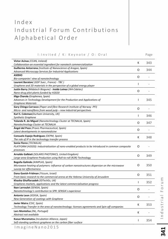
I m a g i n e N a n o 2 0 1 5
Ind
us
tr
ial
Fo
ru
m
34
1
I n d e x
I n d u s t r i a l F o r u m C o n t r i b u t i o n s
A l p h a b e t i c a l O r d e r
I : I n v i t e d / K : K e y n o t e / O : O r a l Page
Victor Acinas (CCAN, Ireland)
Collaboration-an essential ingredient for nanotech commercialization K 343
Guillermo Antorrena (Institute of Nanoscience of Aragon, Spain)
Advanced Microscopy Services for Industrial Applications O 344
ASEBIO Bio-companies' view of nanotechnology
O -
Laurent Baraton( (GDF Suez , France) - TBC )
Graphene and 2D materials in the perspective of a global energy player I -
Justin Barry (Midatech Biogune) - Iraida Loinaz (IK4-Cidetec)
Nano-drug pilot plants funded by H2020 O -
Iñigo Charola (Graphenea, Spain)
Advances in Technology Development for the Production and Applications of
Graphene Materials I 345
Gary Chinga-Carrasco (Paper and fibre Research Institute of Norway -PFI)
Micro- and nanofibres from wood pulp – new industrial perspectives O -
Karl S. Coleman(Durham University, UK)
Synthetic Graphene I 346
Yolanda R. de Miguel (Nanotechnology Cluster at TECNALIA, Spain)
Nanotechnology Cluster at TECNALIA O 347
Ángel del Pozo (Praxis Pharmaceutical, Spain)
Latest developments in nanomedicine O -
Consuelo Espejo Rodriguez (OEPM, Spain)
The role of IP in the technology transfer process K 348
Sonia Florez (TECNALIA)
PLATFORM (H2020): Industrialization of nano-enabled products to be introduced in common composite
processes O -
Arnaldo Galbiati (SOLARIS PHOTONICS, United Kingdom)
Large-area Graphene Production using Roll-to-roll (R2R) Technology O 349
Begoña Galindo (AIMPLAS, Spain)
Microwave heating of polymers: influence of carbon nanostructures dispersion on the microwave
suscep tor effectiveness
O 350
Dana Gavish-Fridman (Yissum, Israel)
From basic research to the commercial arena at the Hebrew University of Jerusalem O 351
Khasha Ghaffarzadeh (IDTechEx, UK)
Graphene-markets, applications and the latest commercialisation progress I 352
Iban Larroulet (SENSIA, Spain)
Nanotechnology's contribution to SPR: SENSIA's experience O -
Antonio Leon (IEDISA, Spain)
New Generation of coatings with Graphene O -
Javier Maira (CSIC, Spain)
Technology Transfer in the area of nanotechnology: licenses agreements and Spin-off companies K 353
Lars Montelius (INL, Portugal)
Abstract not available K -
Kazuo Muramatsu (Incubation Alliance, Japan)
Self-standing synthesis graphene on the carbon fiber surface I 354

I m a g i n e N a n o 2 0 1 5
Ind
us
tr
ial
Fo
ru
m
34
2
I : I n v i t e d / K : K e y n o t e / O : O r a l Page
Cristina Oyón (SPRI, Spain) Nanotechnology and Health in the Basque Country's RIS3 Strategy
O -
Antxon Santamaría (Polymat) Polymers which contain conductive nanoparticles: challenges and hopes for novel (industrial)
applications
O -
Michel Schenker (OMYA) Potential composite applications for pigmented micro- and nano-fibrillated cellulose (MNFC) - an
overview
O -
Ania Servant (NGI-University of Manchester, UK)
The route to Graphene Commercialization I 355
Yoram Shkedi (Melodea Bio-Based Materials) Nano Crystalline Cellulose
O -
Bartolomé Simonet (Carbures) Nanocomposites and the Automotive Sector
O -
Karlheinz Strobl (CVD Equipment Corporation, USA)
Graphene Innovations Drive Nano Material Manufacturing Technologies I 356
Chun-Yun Sung (Lockheed Martin, USA)
Graphene and New 2D Materials: Industry Needs and Commercialization I 357
Nava Swersky Sofer (ICA, Israel)
Abstract not available K -
Ken Teo (Aixtron, UK)
Industry Perspective on Thin Film Graphene Growth I 359
Ashot Ter-Avanessov (OCSiAL Ltd., UK)
Single Wall Carbon Nanotubes Large Scale Production: Bridged the Gap From Lab Potential to
Commercial Reality
I 360
Álvaro Tejado (Tecnalia Research and Innovation)
Introduction to Nanocellulose O -
Laura Toledo (Fundación Argentina de Nanotecnología, Argentina)
Building pillars for NanoTech-transfer in Argentina: networking for acceleration O 361
Iñaki Ugarte (Basque Country Paper Cluster)
The paper sector in the Basque Country O -
Shyam Venkataraman (BASF, Germany)
Performance of graphene materials in energy storage applications I 362

I m a g i n e N a n o 2 0 1 5
Ind
us
tr
ial
Fo
ru
m
3
43
C o l l a b o r a t i o n - a n e s s e n t i a l i n g r e d i e n t
f o r n a n o t e c h c o m m e r c i a l i z a t i o n
CCAN - Collaborative Centre for Applied Nanotechnology
Tyndall National Institute, Cork, & CRANN, TCD, Dublin, Ireland
Europe is a world leader in nanotechnology
research but is lagging behind in its industrial
adoption. More efficient ways to access dispersed
resources and open potential opportunities are
needed for industry to trigger innovative
nanotech-enabled value chains. This will enable
stronger European performance in nano-
commercialization and greater industrial benefit
from nano-enabled products.
This talk presents the experience of CCAN in
designing and implementing a multi-sectoral and
multidisciplinary approach to the translation of
nanotechnology expertise to industry. This
approach has facilitated efficient collaboration by
combining product and market knowledge of
companies with nanotech expertise of research
providers. Furthermore, it has enabled large
enterprises and SMEs to establish, participate and
upgrade their positions in nanotech-enabled value
chains.
To illustrate how effective collaboration between
companies and research providers result in novel
nanotechnology-enabled products and solutions, a
number of examples in the ICT and biomedical
industries will be showcased. The presentation will
conclude with a summary of learnings and
recommendations for nano-commercialization
driven by collaboration.
Victor Acinas

I m a g i n e N a n o 2 0 1 5
Ind
us
tr
ial
Fo
ru
m
3
44
A d v a n c e d M i c r o s c o p y S e r v i c e s f o r
I n d u s t r i a l A p p l i c a t i o n s
Laboratory of Advanced Microscopies
Institute of Nanoscience of Aragon
University of Zaragoza (Spain)
The Invention of Scanning Tunnel Microscope in
1981 was fundamental for the emergence of
nanotechnology. Nowadays nanomaterials are in
the market and their development, production
process and quality control also requires the right
characterization tools. The necessary facilities
usually represent very high cost of investment and
maintenance and require highly qualified and
experienced operators. Therefore it is often a good
alternative for companies to use the services of
advanced analysis offered by some laboratories.
Several key tools for the characterization of
nanomaterials are presented including Electron
and Scanning Probe Microscopies and selected
spectroscopic techniques. In order to illustrate
them, selected examples taken from the
Laboratory of Advanced Microscopies (LMA) will
be shown. We will see how these tools can give us
a deep inside in the characterization of samples as
diverse as nanoparticles, polymeric
nanocomposites, thin films, coatings, graphene,
alloys, membranes or functionalized materials.
LMA represents a nice example of a laboratory in
which top level instruments and the expertise of
the scientists and technical staff involved are
offered to researchers from other public and
private research centers and also to professionals
from industrial sectors. The singularity of this
infrastructure in Nanofabrication and Advanced
Microscopy and the vocation of offering it to the
scientific and technological community has been
recently attested by the Spanish Government ICTS
distinction (Spanish acronym from: Instalación
Científico Técnica Singular).
Guillermo Antorrena

I m a g i n e N a n o 2 0 1 5
Ind
us
tr
ial
Fo
ru
m
3
45
A d v a n c e s i n T e c h n o l o g y D e v e l o p m e n t
f o r t h e P r o d u c t i o n a n d A p p l i c a t i o n s o f
G r a p h e n e M a t e r i a l s
Graphenea, Spain
Graphenes will find many uses in both existing and
new applications. A range of grapheme production
technologies are available but focus on a few
promising platforms will be key to develop
successful applications. This strategy will facilitate
the use and advance the performance of graphene
materials. For graphenes to become successful,
several things need to happen:
• Material must be customized to the
specific application
• Production must be scaled up to match
application needs
• Price must reflect value in use
S p e a k e r B i o g r a p h y
Iñigo Charola is Business Development Director at
Graphenea. He has an extensive experience in
industrial related products at marketing and sales
positions. He started his career at ASSA ABLOY, a
global leader in security products, then as Sales
and Marketing Director at an industrial processes
private company. Before joining Graphenea he is
been working in the Electronic Manufacturing
Services industry as a Sales Director. He holds a
Bachelor’s Degree in Business Administration from
University of Wales, a Master in Marketing and
Sales Management from ESIC and an Executive
MBA from Deusto Business School.
C o m p a n y P r o f i l e
Graphenea is a graphene producer that supplies
high quality graphene materials to leading
companies and research laboratories worldwide.
Graphenea is a company established in 2010 as a
joint venture between private investors and
Repsol. Graphenea has an extensive expertise in
the synthesis, characterization and manipulation of
high quality graphene CVD films. We have
developed our own proprietary technology for the
transfer process. In addition, Graphenea
specializes in the synthesis of graphene oxide (GO)
and rGO.
Iñigo Charola

I m a g i n e N a n o 2 0 1 5
Ind
us
tr
ial
Fo
ru
m
3
46
S y n t h e t i c G r a p h e n e
1 Durham University - Applied Graphene Materials, United Kingdom
Graphene has generated much interest owing to
its exceptional electronic properties and high
mechanical strength. This has enabled new types
of electronic devices and composite materials to
be envisaged. The main problem is the availability
of the material and the difficulties associated with
its synthesis and dispersion. Here I will discuss the
synthesis of graphene using a new simple,
convenient and scalable ‘bottom-up’ to produce
few-layer graphene platelets and discuss
dispersion of graphene in variety of matrices for
applications ranging from paints and coatings to
composite materials.
P r o f e s s o r K a r l C o l e m a n
B i o g r a p h y
is a Professor of Chemistry at Durham University
UK and the founder and Chief Scientific Officer of
Applied Graphene Materials.
His work has been recognised with numerous
awards, including the international Royal Society
of Chemistry Entrepreneur of the Year Award 2011
for his development of intellectual property
around the production of graphene, and the Times
Higher Education Research and Innovation Award
2012. Karl established Applied Graphene Materials
in 2010, which is now listed on the FTSE AIM index.
L i n k s
Prof. Karl Coleman Home Page:
http://www.dur.ac.uk/chemistry/staff/profile/?id=
1329
Applied Graphene Materials
http://www.appliedgraphenematerials.com
Karl Coleman
I m a g i n e N a n o 2 0 1 5
Ind
us
tr
ial
Fo
ru
m
3
47
N a n o t e c h n o l o g y C l u s t e r a t T E C N A L I A
Nanotechnology Cluster Leader, TECNALIA, Parque Tecnológico de Bizkaia,
Calle Geldo, Edificio 700, E-48160 Derio – Bizkaia, Spain
TECNALIA has identified NANOTECHNOLOGY as a
key enabling technology for the development of
new products across a range of industrial sectors
such as Construction, Industry & Transport, Health
and Energy & Environment industries.
At TECNALIA, our approach is to generate
knowledge in nanoscience and nanotechnology,
which can lead to high added value materials and
products, ensuring economic impact and job
creation coming from the resulting
nanotechnology-based industrial applications.
Our R&D activities span the industrial value chain
from nanomaterials (e.g. graphene, nanocellulose,
nanoparticles, nanofibers, etc.) to final nano-based
products; taking into account the environmental,
health and safety (EHS) impacts of
nanotechnology.
Dr. Yolanda de Miguel will present the newly
created NANOTECHNOLOGY CLUSTER at TECNALIA,
describing in detail some of its research activities
and experiences in tech transfer.
F i g u r e s
Yolanda R. de Miguel

I m a g i n e N a n o 2 0 1 5
Ind
us
tr
ial
Fo
ru
m
3
48
T h e r o l e o f I P i n t h e t e c h n o l o g y
t r a n s f e r p r o c e s s
1 OEPM, Spain
The 21st Century has been called the Knowledge
Century in several fora, so, producing Knowledge is
a worldwide spread fact that several types of
organizations (institutions, companies, countries…)
are trying to do better than others. The key is then
what to do with that knowledge? The big question
is, how can that raw knowledge be capitalized for
the benefit of the producer? It is very difficult to
find any technical field where the IPR’s are not
taken into account. Nanotechnology (with its
broad technical coverage) is not different.
Industrial Property Rights have become a
cornerstone of any R&D and Commercial strategy.
In the process of internationalization every
company must prepare a thorough strategy to
make the best out of their investment, any conflict
on IPR’s can weak the project and eventually stop
it. It is no surprise how competing companies fight
their way out into the markets using IPR’s either as
a defensive or attacking weapon. In the
Technology Transfer process, when the knowledge
travels from laboratories to markets IPR’s are
regarded as one of the key elements to accomplish
such journey. IP also brings new perspectives to
R&D as patent protected cross-border
technologies are public, standard, classified and
structured. A better knowledge of IPR’s legal basis
can help to strengthen the companies position in
the market.
Consuelo Espejo Rodriguez

I m a g i n e N a n o 2 0 1 5
Ind
us
tr
ial
Fo
ru
m
3
49
L a r g e - a r e a G r a p h e n e P r o d u c t i o n u s i n g
R o l l - t o - r o l l ( R 2 R ) T e c h n o l o g y
1 SOLARIS PHOTONICS, London, U.K.
2 KINGYOUP OPTRONICS, Taipei, Taiwan (R.O.C)
Only 10 years have passed since Geim and
Novoselov first used adhesive tape to isolate
grapheme from graphite, since then, tens of
graphene manufacturing companies have been
created all over the world, which can produce
small graphene sheets as well as large-area, high-
quality graphene films on an industrial scale
exceeding 400 tonnes and 110,000 m2 per year.
The Chemical Vapor Deposition (CVD) technique
produces high-quality graphene films by the
catalytic decomposition of hydrocarbons on a
metal (for example, Cu, Ni, Pt or alloy) surface at
high temperatures, and the films are then
transferred to transparent substrates such as glass
and polymers by etching away the metal or by
non-destructive electrochemical bubbling for
transparent conductive film (TCF) applications. In
this paper we will present state-of-the-art Roll-to-
roll (R2R) CVD growth and transfer techniques that
have been developed to fabricate large-area
graphene for various applications such as
functional coatings, conductive inks, batteries and
supercapacitors, transparent electrodes in touch
panels, displays and photovoltaic devices as well as
for novel flexible electronic devices.
R e f e r e n c e s
[1] Novoselov, K. S. et al. Science 306, (2004)
666–669.
[2] Zhu, Y. W. et al. Adv. Mater. 22, (2010) 3906–
3924.
[3] Novoselov, K. S. et al. Nature 490, (2012) 192–
2001.
[4] Bonaccorso, F., Sun, Z., Hasan, T. & Ferrari, A.
C. Nature Photon. 4, (2010) 611–622.
[5] LKim, K. S. et al. Nature 457, (2009) 706–710.
[6] Li, X. S. et al. Science 324, (2009) 1312–1314.
[7] Bae, S. et al. Nature Nanotech. 5, (2010) 574–
578.
[8] Kobayashi, T. et al. Appl. Phys. Lett. 102,
(2013) 023112.
[9] Gao, L. B. et al. Nature Commun. 3, (2012)
699.
[10] Dai, B. Y. et al. Nature Commun. 2, (2011) 522.
F i g u r e s
Figure 1: Large-area Graphene production equipment using Roll-to-
roll (R2R) technology.
Arnaldo Galbiati1, James Huang
2

I m a g i n e N a n o 2 0 1 5
Ind
us
tr
ial
Fo
ru
m
3
50
M i c r o w a v e h e a t i n g o f p o l y m e r s :
I n f l u e n c e o f c a r b o n n a n o s t r u c t u r e s
d i s p e r s i o n o n t h e m i c r o w a v e
s u s c e p t o r e f f e c t i v e n e s s
1 AIMPLAS Technological Institute of Polymers, Valencia, Spain
2 Instituto de Tecnología de Materiales, Universidad Politécnica de Valencia, 46022
Valencia, Spain
Microwave technology provides an alternative
methodology to conventional heating of polymers.
Two major effects are responsible for the heating
which results from this interaction: dipolar
polarization and conduction. The microwaves do
not interact with the majority of polymeric
materials due the lack of dipolar moment. For this
reason, additives as heating susceptors can be
used to prepare materials able to absorb
microwaves. These additives are conductive, or
have dielectric properties significantly different
from the polymeric matrix. The electric field will
modify the polymer environment and heating
profiles will be different from the base polymer.
Depending on the nature of the susceptor the
material response to the microwaves can be due
to one specific mechanism or combination of
several of them.
The effectiveness of microwave susceptors
depends on the particle size, shape, concentration,
electrical resistivity and the distribution and
dispersion within the polymeric matrix. The most
widely used and effective susceptors are carbon
structures. Other suitable particles as silicium
carbide, titanium dioxide, metal flakes, zinc oxide
or talc have been tried.
In this work it has been studied the effect of
carbon nanostructures as microwave susceptors
dispersed in a polymeric matrix. Polypropylene
was chosen as matrix due its non-polar nature and
microwave transparency. Thermoplastic
composites were prepared by melt mixing
procedure using a co-rotative twin screw extruder.
The effectiveness of heating process was tested
taking into account critical parameters as
susceptor concentration, microwave source and
dispersion quality. In this way, it is possible to
develop products, based on low energy cost
thermoforming processes, selective welding
surfaces, or carbonous coatings.
Begoña Galindo1 , Adolfo Benedito
1,
Fernando Ramos2 , Enrique
Gimenez2

I m a g i n e N a n o 2 0 1 5
Ind
us
tr
ial
Fo
ru
m
3
51
F r o m b a s i c r e s e a r c h t o t h e c o m m e r c i a l
a r e n a a t t h e H e b r e w U n i v e r s i t y o f
J e r u s a l e m
Yissum, Israel
Nanotechnology-based research at the Hebrew
University was successfully commercialized by
Yissum, the Hebrew University Technology
Transfer Company over the past decades. This talk
will focus on the challenges and models of the
technology transfer work. In other words: how to
bring scientific inventions to the commercial
arena?
Yissum was founded in 1964 to protect and
commercialize the Hebrew University’s intellectual
property. Products based on Hebrew University
technologies that have been commercialized by
Yissum currently generate $2 Billion in annual
sales.
Ranked among the top technology transfer
companies in the world, Yissum has registered
over 8, 0 patents covering 2, 00 inventions; has
licensed out 7 5 technologies and has spun out 9
companies. Yissum’s business partners span the
globe and include companies such as Novartis,
Microsoft, Johnson & Johnson, Merck, Intel, Teva
and many more
Dana Gavish-Fridman

I m a g i n e N a n o 2 0 1 5
Ind
us
tr
ial
Fo
ru
m
3
52
G r a p h e n e - m a r k e t s , a p p l i c a t i o n s a n d
t h e l a t e s t c o m m e r c i a l i s a t i o n p r o g r e s s
1 IDTechEx Ltd, Downing Park, Station Road, Swaffham Bulbeck, Cambridge, CB25
0NW, U.K.
2014 has been an eventful year for the graphene
industry. The first round of commercial
applications has already been announced, and the
industry has witnessed intense investment and
acquisition activity while further companies have
gone public. Despite the high interest, the
valuation of public graphene companies has been
on the decline, returning largely to where they
were at the time of their IPOs.
The graphene community continues to dream up a
steady and divergent pipeline of long-term
applications. Despite this, there is still a lack of the
so-called ‘killer application’ and the suppliers are
pursuing a subsection go-to-market strategy.
We find that today commercial players have more
realistic expectations, showing a convergence of
focus on composite and energy storage
applications and en-mass migration further
downstream to offer intermediary products.
IDTechEx, an independent market research
company focused on emerging technologies, has
been tracking the graphene and carbon nanotube
markets for several years. In this talk, IDTechEx will
outline the following
1- Latest news in the industry including product
announcements, investments/floatations and
acquisitions
2- Latest commercial trends in the graphene
industry
a. Emergence of China
b. Strength of demand in Korea
c. Convergence on battery and composite
applications
d. Migration downstream
3- Production capacity by supplier and the
condition of over-capacity
4- Learning from where carbon nanotubes had
success
a. Electrostatic painting of car parts
b. Fuel systems in cars
c. Battery electrode additives
5- Application pipeline
6- Ten-year segmented market projections
Khasha Ghaffarzadeh, Harry Zervos

I m a g i n e N a n o 2 0 1 5
Ind
us
tr
ial
Fo
ru
m
3
53
T e c h n o l o g y T r a n s f e r i n t h e a r e a o f
n a n o t e c h n o l o g y : l i c e n s e s a g r e e m e n t s
a n d S p i n - o f f c o m p a n i e s
1 Vicepresidencia Adjunta de Transferencia de Conocimiento, Consejo Superior de
Investigaciones Científicas (CSIC), Serrano 142, Madrid, Spain
In the last seven years CSIC has launched a series
of actions whose objective was to take advantage
of the knowledge generated in R&D projects,
through its transfer to industry to bring out high
value products and services to the market [1]. Due
to all this effort CSIC has been able to sign 47
patent license agreements with companies in the
last 4 years for the exploitation of its
nanotechnologies in the market, which represent a
percentage of 17% over the total number of
licenses agreements signed by CSIC in this specific
period. In addition, 16 spin-off companies have
been created based on CSIC nanotechnologies
since 2004.
In this presentation the transferred technologies
will be analyzed in terms of its application in the
industrial sectors. Some specific cases of
nanotechnologies that have been transferred to
the industrial sector will be presented:
incorporation of security components in credit
cards and passports by using invisible nanometer-
thick layer or nanoparticles, remove of toxic
pollutants by using new materials functionalized
with nanoparticles, new equipment for the
fabrication or characterization of nanoparticles,
use of nanocapsules for different applications, new
ways for the fabrication of graphene and graphene
nanocomposites, etc.
This presentation shows how the
nanotechnologies developed in public research
organizations can be implemented in the industry
to introduce new products or services in the
market.
R e f e r e n c e s
[1] Javier Etxabe, Javier Maira y Pedro A. Serena,
Mundonano Vol. 5 n.9 (2012) 31-56.
F i g u r e s
Figure 1: Evolution of the number of CSIC licensed patents in
nanotechnology.
Javier Maira and Javier Etxabe

I m a g i n e N a n o 2 0 1 5
Ind
us
tr
ial
Fo
ru
m
3
54
S e l f - s t a n d i n g s y n t h e s i s g r a p h e n e o n
t h e c a r b o n f i b e r s u r f a c e
1 Incubation Alliance,Inc. 1-2-25-D307, Wadayama-dori, Hyogo-ku, Kobe 6520884
Japan
Graphene has unique characteristics chemically,
biochemically and physically with flat monolayer
2D structure. To put graphene into practical use
taking advantage of these unique properties, it is
required to maintain the self-standing structure
while preventing aggregation, stacking and
adhesion of graphene due to Van der Waals force.
If graphene is stably stacked in multiple layers,
graphite is formed, and advantageous functions of
graphene are lost.
CVD reaction to obtain graphene by calcinations of
raw material derived from phenol resin fiber heat-
treated moderately and the remaining hydrogen
content adjusted under high-pressure and
isotropic gas pressure [1]. H2 and CH4 generated
from the raw materials of calcined resin fiber form
the graphene on the fiber surface without any
catalyst. It is possible to form a few layers of
grapheme showing self-standing structure on all of
carbon fiber surface which is simultaneously
carbonized. In this synthetic process, yarn, woven
cloth, non-woven cloth and other types of resin
fibers are applicable, and graphene formed on the
surface of these fibers have identical self-standing
stable structure.
The self-standing synthesized graphene on the
carbon fiber cloth is directly used for the electrode
of field emission devices [2], secondary batteries
and fuel cells exhibiting unique performance.
R e f e r e n c e s
[1] K. Muramatsu, K. Sutani and M. Toyoda,
Graphene2012 International Conference,
Brussels, Belguim, 2012.4.10-13.
[2] Yusuke Iwai, Kazuo Muramatsu, Shougo
Tsuboi, Atsuo Jyouzuka, Tomonori Nakamura,
Yoshihiro Onizuka and Hidenori Mimura, 2013
Appl. Phys. Express 6 105102
F i g u r e s
Figure 1: Self-standing synthesis graphene on the carbon fiber
surface.
Kazuo Muramatsu
I m a g i n e N a n o 2 0 1 5
Ind
us
tr
ial
Fo
ru
m
3
55
T h e r o u t e t o g r a p h e n e
c o m m e r c i a l i s a t i o n
1 the University of Manchester, U.K.
Graphene - the so called "wonder material" could
change the world with what seems endless
applications and capabilities. Challenges exist in
achieving this commercialisation and a key will be
the creation of partnerships and collaborations to
make these real from structures, to membranes
and electronic applications. The principle of “open
Innovation” together with the critical investments
in the National Graphene Institute and Graphene
Engineering Innovation Centre at The University of
Manchester will provide a world leading centre for
Graphene research and support the development
of applications and business opportunities through
partnerships with industry.
About Ania Servant
After completion of Master of Sciences (MSc.)
from the Ecole Nationale Superieure de Chimie de
Paris (Chimie Paris-Tech), followed by a Master of
Research (MRes.) from Pierre et Marie Curie
University (Paris VI), Ania was awarded a Marie
Curie Fellowship to pursue a PhD training in Queen
Mary University on the development of novel
micro/nanoparticles for catalysis and biomimetic
applications. After completion of her PhD in June
2010, Ania worked as a post-doctoral research
associate for over two years in the Nanomedicine
Lab at UCL School of Pharmacy, under the
supervision of Prof. Kostas Kostarelos,
functionalising carbon nanomaterials including
graphene and carbon nanotubes for biomedical
applications such as novel delivery vectors and
diagnostic agents. In November 2012, she was
awarded of a EPSRC Post-doctoral Fellowship to
pursue her studies for another year in the
Nanomedicine lab on the development of
injectable graphene hydrogel hybrids for on-
demand drug delivery.
From December 2013, Ania works as Knowledge
Exchange fellow for the National Graphene
Institute at the University of Manchester. Her role
aims at generating opportunities for knowledge
exchange between the NGI and
industrial/commercial partners and participating in
the development of a sustainable, long term
knowledge exchange capability within this
institute. As such, Dr. Servant will be involved in
conducting a number of short term applied
projects in partnership with a diverse range of
industrial partners looking to investigate the use of
graphene and its derivatives in a range of
applications. In addition, she will be involved in co-
ordinating larger scale externally funded
knowledge exchange application projects and in
contributing to these projects in collaboration with
colleagues from the School of Materials, Physics,
Computer Science, Bio and Life Sciences, and other
university departments.
Ania Servant
I m a g i n e N a n o 2 0 1 5
Ind
us
tr
ial
Fo
ru
m
3
56
G r a p h e n e I n n o v a t i o n s D r i v e N a n o
M a t e r i a l M a n u f a c t u r i n g T e c h n o l o g i e s
1 CVD Equipment Corporation, 355 S. Technology Drive, Central Islip
New York 11722, USA
Many different processing methods have been
demonstrated over the last 20 year for 1D and 2D
nanomaterial manufacturing. Worldwide interest
over the last 10 years has been focused on
advancing the state of the art and quality of CVD
graphene manufacturing. A wide range of CVD
manufacturing methods and equipment solutions
have been explored and their respective benefits
and drawback analyzed in relation to the quality
and scalability of CVD graphene material.
Worldwide focus in manufacturing processes for
high performance wavelength-division
multiplexing (WDM) filter technology in 1995-2005
advanced the optical thin film coating industry by
developing real time inline optical monitoring
systems. Similarly, CVD graphene manufacturing
processes are the driving force behind recent
innovations in CVD equipment. The knowledge
gained in solving CVD graphene equipment and
processes are often adaptable to advancing the
manufacturing and commercialization of other
nano materials.
We will report here how our CVD graphene
research, processing and equipment innovations
have
inspired a similar advancement in nano material
manufacturing scale-ups in VACNT’s and SiNW’s.
We will also show, by example how challenges in
utilizing Ethanol as a liquid precursor to create a
more reproducible bilayer of CVD graphene
inspired us to enhance our CVDWinPrC™ control
software to provide real time diagnostic feedback
control for all types and sizes of liquid Bubblers. To
do this we developed an online Bubbler fill level
software/hardware solution that determines the
Bubbler fill level accuracy to better than 0.5% and
also measures the Bubbler vapor pickup efficiency
to better than 5%. This and other CVD system tests
are now automated and can be run after hours or
between production runs as desired to make sure
the liquid precursor delivery is reproducible. It also
enables process recipes based on measured
Bubbler efficiencies and can help all CVD processes
that utilize a Bubbler as a precursor source.
Karlheinz Strobl, Mathieu Monville,
Riju Singhal, Samuel Wright
I m a g i n e N a n o 2 0 1 5
Ind
us
tr
ial
Fo
ru
m
3
57
G r a p h e n e a n d N e w 2 D M a t e r i a l s :
I n d u s t r y N e e d s a n d C o m m e r c i a l i z a t i o n
1 Technical Director of Advanced Technologies, Mission, Systems and Training (MST)
199 Borton Landing Road, PO Box 1027 M/S 101-125, Moorestown, NJ 08057-0927
Corporate Engineering and Technology Operation (CETO)
6801 Rockledge Drive, MP 363, Bethesda, MD 20817
Lockheed Martin (LM) is seeking to establish a
multidisciplinary and internationally collaboration
devoted to the design and development of
advanced two-dimensional (2D) layered materials.
The effort will synergistically integrate each LM
business units with academic, research institute,
government and leading national/international
Industries. We will review industrial needs for
defense and IT communities and define
applications in key strategic areas for national
interests in materials, devices and systems.
The successful collaborations between academia,
government and industry will yield opportunities in
nanomaterials, define transformational goals and
impact to nanotechnology. The talk outlines
include:
• Overview Industry Needs
• Review Achievements in Graphene
• New 2D Material Developments
• Outlook / Opportunities in 2D Materials
• Commercialization and Challenges
2D materials exhibit a variety of unique properties
different from bulk that will enhance the
performance of existing technologies and enable
future potentials. The outstanding characteristics
also suggest that these materials could provide
new possibilities in analog and digital electronics,
optoelectronics, multifunctional sensors and
actuators, shielding, energy storage/harvesting,
anticorrosion, oxidation, abrasion, friction,
extreme environmental tolerance,
biocompatibility, and transport properties,
especially with ultrathin scales. However, the
fundamental study of synthesis, integration,
properties, processing techniques and scale-up
ability of these novel material systems is still in
development phases and required for the success
of scientific innovation. The developments of novel
2D materials such as graphene, MoS2, WS2, hBN,
and WSxSe1-x should leverage and ensure close
academic-industrial collaborations. Furthermore,
the cross-cutting knowledge and close industrial
partnership between the equipment
manufacturers, material suppliers, semiconductor
companies, small businesses and large
corporations will result in a unique synergistic
alliance to further exploit the unprecedented
physical properties of 2D nanomaterials and
revolutionize multifunctional technologies. The
pursuits should have the following activities:
performing transformational and application
oriented R&D, developing IPs, establishing low cost
and high quality nanomanufacturing capabilities.
For this effort, LM’s advanced materials and
nanotechnology develop ultimate visions to:
Enable affordable and highly scalable applications
in air, space, on land, at sea with multifunctional
performance superior to conventional materials;
Shift paradigms in multiple industries like energy,
sensing, and computing as well as fundamental
manufacturing; Generate materials-by-design
capabilities for unmatched technological
advantage in our core market, blazing major trails
into multiple adjacent and horizon markets. Our
clear missions are to coordinate and leverage
advanced materials and nanotechnology
development efforts and capabilities to capture
and maintain technological leadership and drive
technology transition consistent with defense
priorities and key promising adjacencies that will
both strengthen our leadership position and
support continuing, cutting-edge research and
development in this domain. The major focus
development areas for novel 2D materials cover
Nanomaterials and Manufacturing (revolutionary
C.Y. (Chun-Yung) Sung

I m a g i n e N a n o 2 0 1 5
Ind
us
tr
ial
Fo
ru
m
3
58
multifunctional structures, enable low-cost
manufacturing); Energy (cables and wiring,
advanced batteries and supercapacitors); Sensors
and Electronics (broad-band infrared sensors,
flexible electronics); Modeling and Advanced
Computations (enable bio-mimetics; computers as
powerful as the brain); Adaptation and Stealth.
We will illustrate the following three approaches:
Advance S&T Discovery -Enable exploration for
new technology development to strengthen our
ability to provide innovative and affordable
solutions into our core products while supporting
technology development for adjacent markets and
business growth; Build Global Technology
Partnerships –Create/build partnerships globally/
across the company to accelerate technology
integration and transition. Reduce risk and
optimize our return on investment through
effective scouting and key university, small
business, and S&T customer relationships; Catalyze
S&T Collaboration Opportunities - Focus on
nanomaterial innovations through strong S&T
Engagements, data analytics and information
milestones to advance game changing
technologies and support technology transition
while sustainably growing our capability of today
and tomorrow.
F i g u r e s

I m a g i n e N a n o 2 0 1 5
Ind
us
tr
ial
Fo
ru
m
3
59
I n d u s t r y P e r s p e c t i v e o n T h i n F i l m
G r a p h e n e G r o w t h
AIXTRON Ltd - Anderson Road, Swavesey, Cambridge, CB24 4FQ, United Kingdom
In the recent years, graphene has attracted the
attention of a considerable number of scientists
from all scientific areas. The unique properties of
this two dimensional material which include, high
carrier mobility, electrical conductivity,
transparency, thermal conductivity and mechanical
strength, make thin film graphene as a prominent
candidate for novel electronic, opto and sensing
applications.
This presentation puts into perspective thin film
graphene growth technology by chemical vapour
deposition and compares it with other depositions
technologies at AIXTRON. We start with examined
the published growth mechanisms for graphene
and use this as the key development drivers for
deposition equipment features.
Growth results are presented from small scale up
to 300mm wafer scale. The use of in-situ growth
monitoring and graphene electronic and opto
device results are also presented.
Finally, three different integration schemes and
value chain opportunities for graphene thin film
production are discussed
Kenneth B. K. Teo

I m a g i n e N a n o 2 0 1 5
Ind
us
tr
ial
Fo
ru
m
3
60
S i n g l e W a l l C a r b o n N a n o t u b e s L a r g e
S c a l e P r o d u c t i o n : B r i d g e d t h e G a p
F r o m L a b P o t e n t i a l t o C o m m e r c i a l
R e a l i t y
OCSiAL Ltd., UK
Carbon nanomaterials, studied by thousands of
researchers and companies around the world,
continue to hold the promise to usher in a new era
of materials technology. The use of SWCNTs could
open the door to fundamental change in many
industries, but there has always been an invincible
obstacle: SWCNTs were only available in small
quantities at sky-high prices, and quality wasn’t
guaranteed.
In 2014 OCSiAl, an international technology firm
headquartered in Luxembourg, unveiled a
breakthrough technology for the production of
single wall carbon nanotubes (‘SWCNTs’), which
enables large scale, commercial production of
SWCNT for the first time. The output, ‘as
produced,’ under the brand name TUBALL, yields
75% and more of top quality SWCNTs, with all
impurities of catalyst particles encapsulated in
carbon shells. The content of free metal particles
does not exceed 1%. Numerous laboratory and
industrial tests proved TUBALL’s ability to serve as
a first universal additive, enhancing mechanical
strength and the thermal and electrical
conductivity of materials, such as composites,
polymers, rubbers, metals, batteries, transparent
conductive films and many others. Significant
improvements in performance of these and other
materials are observed upon the addition of
0.001%-0.1% weight of TUBALL. The commercial
price for TUBALL is 50 times lower than of other
products with similar properties. Potential annual
capacity of OCSiAl production is currently 10
tonnes. This method is easily scalable and capable
of producing an unlimited quantity of SWCNTs at a
very low cost.
With this production volume and ultimately the
quality of the end product, OCSiAl technology is
poised to improve many of the products the world
relies on. OCSiAl helps make nanotechnology
applicable for many companies desperate for a
commercially viable materials innovation.
Ashot Ter-Avanessov

I m a g i n e N a n o 2 0 1 5
Ind
us
tr
ial
Fo
ru
m
3
61
B u i l d i n g p i l l a r s f o r N a n o T e c h - t r a n s f e r
i n A r g e n t i n a : n e t w o r k i n g f o r
a c c e l e r a t i o n
1 FAN, Argentina
Argentinean Nanotechnology Foundation (FAN)
has been working on the basis for innovation since
2007. Traditionally, FAN has carried out activities
to strengthen national innovation processes
through nanotechnology, such as encouraging
scientists to work towards nanotechnology
transfer, stimulating entrepreneurs and
manufacturers through investment, and
accelerating new business providing facilities at its
nano-maker space.
Based on this experience, nowadays, FAN is
coordinating, on behalf of the Ministry of Science,
Technology and Productive Innovation, a national
initiative financed by European Union, to obtain
new nanotech-products and launch them into the
market before December of 2015. For this
purpose, FAN has joint more than 30 entities
(among SMEs companies, national research
centers and European technological centers). FAN
recognizes on Cooperation another substantial
pillar for tech-transfer.
Laura Toledo
I m a g i n e N a n o 2 0 1 5
Ind
us
tr
ial
Fo
ru
m
3
62
P e r f o r m a n c e o f g r a p h e n e m a t e r i a l s i n
e n e r g y s t o r a g e a p p l i c a t i o n s
BASF SE, Ludwigshafen, Germany
In BASF at the Carbon Materials Innovation Center
(CMIC), advanced carbon materials are being
investigated for several potential fields of
application such as electronics, catalysis, and
energy storage and conversion devices. Graphene,
one such advanced and emerging carbon material
has recently spurred strong interest of scientific
research both in academia and industry owing to
its remarkable properties. For example, owing to
its higher electrical conductivity, graphene is
proposed as a new carbon material to replace or
complement traditional carbon black additives in
lithium-ion batteries as well as activated carbon in
supercapacitor devices. Recent results from our
lab using few layers graphene (FLG) in
electrochemical capacitor and lithium ion battery
applications will be presented. In electrochemical
capacitor applications, FLG shows higher power
density and lower energy density compared to the
state of the art activated carbon. In lithium ion
battery applications, addition of FLG materials to
anode formulation containing silicon (Si) anode
slurries leads to improvement in capacity fading.
Finally the talk will present the challenges lie
ahead for the commercialization of FLG to make it
to reality in the near future.
S p e a k e r B i o g r a p h y
Dr. Shyam S. Venkataraman is the Project Manager
in CMIC at BASF SE, Germany. He received his
Bachelor of Technology in Chemical and
Electrochemical Engineering from Central Electro
Chemical Research Institute (CECRI), India (2004),
Master of Science in Analytical Chemistry from
University of North Texas (2007), USA and PhD in
Analytical Chemistry from Clarkson University
(2012), USA. He worked as R&D manager at BASF
Electronic Materials, Taiwan from 2010 to 2012.
Since April 2012, he is leading a team in CMIC
focusing on the preparation of advanced carbon
materials and its application in energy storage and
conversion devices. He has given 20 scientific
presentations, filed 20 patent applications and co-
authored 6 scientific papers in the area of
graphene electrochemistry, copper electro-
deposition and corrosion, formulation of silica and
ceria polishing slurries and wafer cleaning
solutions for hard disk drive and integrated circuits
fabrication.
Shyam S. Venkataraman

E d i t e d b y
Calle Alfonso Gomez, 17, Planta 2 - Loft 16
28037 Madrid – Spain
Email: [email protected]
Web: www.phantomsnet.net


