Freescale SemiconductorApplication Note
© Freescale Semiconductor, Inc., 2009. All rights reserved.
1 IntroductionThis document describes how to initialize and maintain the Real Time Clock (RTC) on the i.MX25. The RTC is a digital clock which can be used to accurately keep track of the current time. Some benefits of having an embedded real time clock include:
• Low power consumption (since the RTC on the i.MX25 can run from a coin cell battery)
• Frees the ARM® core to do tasks other than time keeping
• Continues to keep time even while the i.MX25 is powered down
This application note is intended for non-security customers with non-secure devices. For customers who require security to be enabled, refer to the i.MX258 Security Reference Manual for detailed information on how to use the RTC and DryIce module.
Document Number: AN3874Rev. 0, 06/2009
Contents1. Introduction . . . . . . . . . . . . . . . . . . . . . . . . . . . . . . . . . 12. Real Time Clock . . . . . . . . . . . . . . . . . . . . . . . . . . . . . 23. External Signal Description . . . . . . . . . . . . . . . . . . . . 34. Memory Map and Register Definition . . . . . . . . . . . . 35. Example . . . . . . . . . . . . . . . . . . . . . . . . . . . . . . . . . . 146. Revision History . . . . . . . . . . . . . . . . . . . . . . . . . . . . 16
i.MX25 Real Time Clock (RTC)by Multimedia Applications Division
Freescale Semiconductor, Inc.Austin, TX
i.MX25 Real Time Clock (RTC), Rev. 0
2 Freescale Semiconductor
Real Time Clock
2 Real Time ClockThe RTC on the i.MX25 device is embedded as part of the DryIce module. Even though the DryIce is a security module, the RTC function is still available as part of the i.MX25.
The RTC is a 47-bit time counter which runs from the 32.768 KHz clock source. The 15 least significant bits count the number of clock cycles in each second while the 32 most significant bits count the number of seconds. The RTC also includes a programmable 47-bit clock alarm with an interrupt which can be used as a system wake-up from low power mode or as a general interrupt at a pre-defined time. Additionally the RTC includes a general purpose 32-bit register to allow storing of data during system power down assuming the RTC remains powered by the backup battery (BAT_VDD).
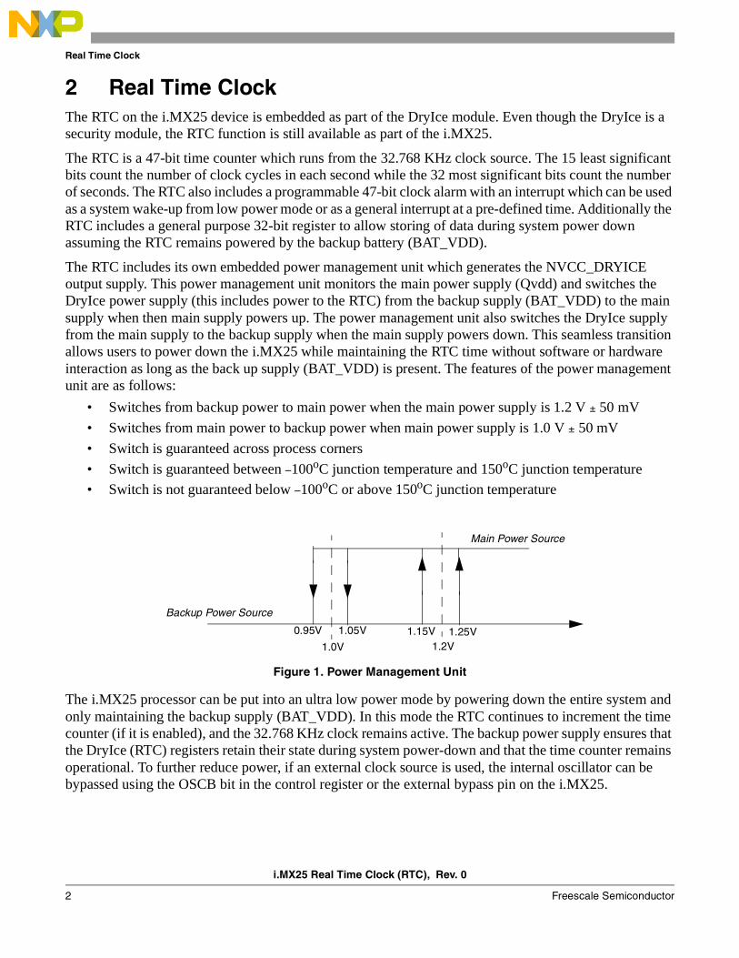
The RTC includes its own embedded power management unit which generates the NVCC_DRYICE output supply. This power management unit monitors the main power supply (Qvdd) and switches the DryIce power supply (this includes power to the RTC) from the backup supply (BAT_VDD) to the main supply when then main supply powers up. The power management unit also switches the DryIce supply from the main supply to the backup supply when the main supply powers down. This seamless transition allows users to power down the i.MX25 while maintaining the RTC time without software or hardware interaction as long as the back up supply (BAT_VDD) is present. The features of the power management unit are as follows:
• Switches from backup power to main power when the main power supply is 1.2 V ± 50 mV
• Switches from main power to backup power when main power supply is 1.0 V ± 50 mV
• Switch is guaranteed across process corners
• Switch is guaranteed between –100oC junction temperature and 150oC junction temperature
• Switch is not guaranteed below –100oC or above 150oC junction temperature
Figure 1. Power Management Unit
The i.MX25 processor can be put into an ultra low power mode by powering down the entire system and only maintaining the backup supply (BAT_VDD). In this mode the RTC continues to increment the time counter (if it is enabled), and the 32.768 KHz clock remains active. The backup power supply ensures that the DryIce (RTC) registers retain their state during system power-down and that the time counter remains operational. To further reduce power, if an external clock source is used, the internal oscillator can be bypassed using the OSCB bit in the control register or the external bypass pin on the i.MX25.
Backup Power Source
Main Power Source
1.0V
1.05V0.95V
1.2V1.25V1.15V

i.MX25 Real Time Clock (RTC), Rev. 0
Freescale Semiconductor 3
External Signal Description
3 External Signal DescriptionThe external signals of the RTC are described in Table 1.
4 Memory Map and Register DefinitionThis section includes the module memory map and detailed descriptions of all of the registers.
4.1 Memory MapTable 2 shows the DryIce (RTC) memory map.
Table 1. Signal Properties
Signal Function I/O Reset
BAT_VDD Backup power supply (core voltage level ) for DryIce I —
NVCC_DRYICE DryIce power supply (core voltage level) after switch O —
NGND_DRYICE DryIce ground I/O —
OSC32K_EXTAL 32.768 KHz crystal input I 0
OSC32K_XTAL Oscillator output to the 32.768 KHz crystal O 0
OSC_BYP Bypass the 32.768 KHz oscillator I 0
Table 2. Block Memory Map
Address Register1
1 Includes short name and long name. In this table, the short name appears in the first column.
Access Reset2 Value
2 Reset refers to DryIce POR.
Section/Page
General Registers
0x53FF_C000 (RTCMR)
RTC Time Counter MSB Register (RTCMR) R/W 0x0000_0000 4.1.2.1/6
0x53FF_C004 (RTCLR)
RTC Time Counter LSB Register (RTCLR) R/W 0x0000_0000 4.1.2.2/7
0x53FF_C008 (RCAMR)
RTC Clock Alarm MSB Register (RCAMR) R/W 0x0000_0000 4.1.2.3/7
0x53FF_C00C (RCALR)
RTC Clock Alarm LSB Register (RCALR) R/W 0x0000_0000 4.1.2.4/8
0x53FF_C010 (DCR)
DryIce Control Register (DCR) R/W 0x0000_0000 4.1.2.5/9
0x53FF_C014 (DSR)
DryIce Status Register (DSR) R/W 0x0000_0001 4.1.2.6/10
0x53FF_C018 (DIER)
DryIce Interrupt Enable Register (DIER) R/W 0x0000_0000 4.1.2.7/12
0x53FF_C03C (DGPR)
DryIce General Purpose Register (DGPR) R/W 0x0000_0000 4.1.2.8/14

i.MX25 Real Time Clock (RTC), Rev. 0
4 Freescale Semiconductor
Memory Map and Register Definition
4.1.1 Register SummaryThe conventions in Figure 2 and Table 3 serve as a key for the register summary and individual register diagrams.
Table 3 provides a key for register figures and tables and the register summary.
Table 4 shows the DryIce register summary.
Alwaysreads 1
1 Alwaysreads 0
0 R/Wbit
BIT Read-only bit
BIT Write-only bit
Write 1to clear
BIT Self-clearbit
0 N/A
BIT w1c BIT
Figure 2. Key to Register Fields
Table 3. Register Conventions
Convention Description
Depending on its placement in the read or write row, indicates that the bit is not readable or not writable.
FIELDNAME Identifies the field. Its presence in the read or write row indicates that it can be read or written.
Register Field Types
R Read only. Writing this bit has no effect.
W Write only.
R/W Standard read/write bit. Only software can change the bit’s value (other than a hardware reset).
rwm A read/write bit that may be modified by a hardware in some fashion other than by a reset.
w1c Write one to clear. A status bit that can be read, and is cleared by writing a one.
Self-clearing bit Writing a one has some effect on the module, but it always reads as zero. (Previously designated slfclr)
Reset Values
0 Resets to zero.
1 Resets to one.
— Undefined at reset.
u Unaffected by reset.
[signal_name] Reset value is determined by polarity of indicated signal.
Table 4. DryIce Register Summary
Name31 30 29 28 27 26 25 24 23 22 21 20 19 18 17 16
15 14 13 12 11 10 9 8 7 6 5 4 3 2 1 0
0x53FF_C000 (RTCMR)
RRTC[47:32]
W
RRTC[31:16]
W

i.MX25 Real Time Clock (RTC), Rev. 0
Freescale Semiconductor 5
Memory Map and Register Definition
0x53FF_C004 (RTCLR)
RRTC[15:1]
0
W
R 0 0 0 0 0 0 0 0 0 0 0 0 0 0 0 0
W
0x53FF_C008 (RCAMR)
RRCA[47:32]
W
RRCA[31:16]
W
0x53FF_C004 (RTCLR)
RRCA[15:1]
0
W
R 0 0 0 0 0 0 0 0 0 0 0 0 0 0 0 0
W
0x53FF_C010 (DCR)
R 0 0 0 0 0 0 0 0 0 0 0 0 0 TCHL
TCSL
FSHLW
R
NSAOSCB
0 0 0 0 0 0 0 0 0
APE TCE
0 0 0
WSWR
0x53FF_C014 (DSR)
R 0 0 0 0 0 0 0 0 0 0 0 EBD 0 0 0 0
W w1c
R 0 0 0 0 0WBF
WNF
WCF
WEF
0 0 CAF 0TCO NVF SVF
W w1c w1c w1c w1c w1c
0x53FF_C018 (DIER)
R 0 0 0 0 0 0 0 0 0 0 0 0 0 0 0 0
W
R 0 0 0 0 0 0 WCIE
WCIE
WEIE
0 0 CAIE
0 TOIE
0 0
W
0x53FF_C03C (DGPR)
RGPR[31:16]
W
RGPR[15:0]
W
Table 4. DryIce Register Summary (continued)
Name31 30 29 28 27 26 25 24 23 22 21 20 19 18 17 16
15 14 13 12 11 10 9 8 7 6 5 4 3 2 1 0

i.MX25 Real Time Clock (RTC), Rev. 0
6 Freescale Semiconductor
Memory Map and Register Definition
4.1.2 Register DescriptionsThis section consists of register descriptions in address order. Each description includes a standard register diagram with an associated figure number. Details of register bit and field function follow the register diagrams, in bit order.
DryIce is a security module and some registers could be set to only be accessible by secure software. However the secure registers are accessible by non-secure software when the Non-Secure Access bit in the DryIce Control Register is set. Therefore it is imperative that the non-secure bit is set when using non-secure applications or non-secure i.MX25 devices to ensure proper RTC operation.
With the exception of the DryIce Interrupt Enable Register and the DryIce Status Register bits [11:8], all DryIce registers are clocked by the 32.768 KHz clock source. This limits the maximum throughput of writes to these registers to once every two 32.768 KHz clock cycles and means that the actual register does not update until the third 32.768 KHz clock cycle after the write is performed. The Write Next Flag, Write Busy Flag and Write Completed Flag (with associated interrupts) can be used to determine when a register write has completed and when the next register write can be performed.
The DryIce Interrupt Enable Register and the DryIce Status Register bits [11:8] are clocked by the peripheral bus clock. These register bits update immediately and writing to the DryIce Interrupt Enable Register does not affect the Write Next Flag, Write Busy Flag or Write Completed Flag. In addition, the Write Busy Flag does not need to be clear to write to the DryIce Interrupt Enable Register.
All register reads complete after three or four peripheral clock cycles, returning the data in the register at the time of the register read. Pending writes to that register are not reflected in the data returned unless the write has completed.
4.1.2.1 RTC Time Counter MSB Register (RTCMR)
The RTC Time Counter MSB Register contains the 32 most significant bits (47:16) of the 47-bit RTC Time Counter. Clocked by a 32.768 KHz clock, this register is effectively a 32-bit seconds counter.
See Figure 3 for illustration of valid bits in the RTC Time Counter MSB Register and Table 5 for description of the bit fields.
0x53FF_C000 (RTCMR) Access: Write/ Read
31 30 29 28 27 26 25 24 23 22 21 20 19 18 17 16
RRTC[47:32]
W
RESET 0 0 0 0 0 0 0 0 0 0 0 0 0 0 0 0
15 14 13 12 11 10 9 8 7 6 5 4 3 2 1 0
RRTC[31:16]
W
RESET 0 0 0 0 0 0 0 0 0 0 0 0 0 0 0 0
Figure 3. RTC Time Counter MSB Register
i.MX25 Real Time Clock (RTC), Rev. 0
Freescale Semiconductor 7
Memory Map and Register Definition
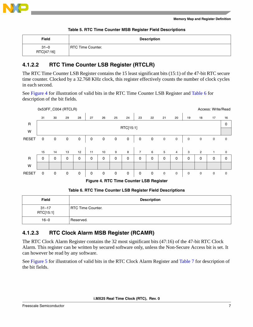
4.1.2.2 RTC Time Counter LSB Register (RTCLR)
The RTC Time Counter LSB Register contains the 15 least significant bits (15:1) of the 47-bit RTC secure time counter. Clocked by a 32.768 KHz clock, this register effectively counts the number of clock cycles in each second.
See Figure 4 for illustration of valid bits in the RTC Time Counter LSB Register and Table 6 for description of the bit fields.
4.1.2.3 RTC Clock Alarm MSB Register (RCAMR)
The RTC Clock Alarm Register contains the 32 most significant bits (47:16) of the 47-bit RTC Clock Alarm. This register can be written by secured software only, unless the Non-Secure Access bit is set. It can however be read by any software.
See Figure 5 for illustration of valid bits in the RTC Clock Alarm Register and Table 7 for description of the bit fields.
Table 5. RTC Time Counter MSB Register Field Descriptions
Field Description
31–0RTC[47:16]
RTC Time Counter.
0x53FF_C004 (RTCLR) Access: Write/Read
31 30 29 28 27 26 25 24 23 22 21 20 19 18 17 16
RRTC[15:1]
0
W
RESET 0 0 0 0 0 0 0 0 0 0 0 0 0 0 0 0
15 14 13 12 11 10 9 8 7 6 5 4 3 2 1 0
R 0 0 0 0 0 0 0 0 0 0 0 0 0 0 0 0
W
RESET 0 0 0 0 0 0 0 0 0 0 0 0 0 0 0 0
Figure 4. RTC Time Counter LSB Register
Table 6. RTC Time Counter LSB Register Field Descriptions
Field Description
31–17 RTC[15:1]
RTC Time Counter.
16–0 Reserved.

i.MX25 Real Time Clock (RTC), Rev. 0
8 Freescale Semiconductor
Memory Map and Register Definition
4.1.2.4 RTC Clock Alarm LSB Register (RCALR)
The RTC Clock Alarm Register contains the 15 least significant bits (15:1) of the 47-bit RTC Clock Alarm. This register can be written by secured software only, unless the Non-Secure Access bit is set. It can however be read by any software.
See Figure 6 for illustration of valid bits in the RTC Clock Alarm Register and Table 8 for description of the bit fields.
0x53FF_C008 (RCAMR) Access: Write/Read
31 30 29 28 27 26 25 24 23 22 21 20 19 18 17 16
RRCA[47:32]
W
RESET 0 0 0 0 0 0 0 0 0 0 0 0 0 0 0 0
15 14 13 12 11 10 9 8 7 6 5 4 3 2 1 0
RRCA[31:16]
W
RESET 0 0 0 0 0 0 0 0 0 0 0 0 0 0 0 0
Figure 5. DryIce Clock Alarm Register
Table 7. DryIce Clock Alarm Register Field Descriptions
Field Description
31–0RCA[47:16]
RTC Clock Alarm.
0x53FF_C00C (RCALR) Access: Write/Read
31 30 29 28 27 26 25 24 23 22 21 20 19 18 17 16
RRCA[15:1]
0
W
RESET 0 0 0 0 0 0 0 0 0 0 0 0 0 0 0 0
15 14 13 12 11 10 9 8 7 6 5 4 3 2 1 0
R 0 0 0 0 0 0 0 0 0 0 0 0 0 0 0 0
W
RESET 0 0 0 0 0 0 0 0 0 0 0 0 0 0 0 0
Figure 6. RTC Clock Alarm Register

i.MX25 Real Time Clock (RTC), Rev. 0
Freescale Semiconductor 9
Memory Map and Register Definition
4.1.2.5 DryIce Control Register (DCR)
The DryIce Control Register (DCR) contains all of the necessary control bits for the DryIce module. This register can only be read or written by secured software, unless the Non-Secure Access bit is set.
See Figure 7 for illustration of valid bits in the DryIce Control Register and Table 9 for description of the bit fields.
Table 8. DryIce Clock Alarm Register Field Descriptions
Field Description
31–0DCA[15:1]
RTC Clock Alarm.
0x53FF_C010 (DCR) Access: Secure read/write
31 30 29 28 27 26 25 24 23 22 21 20 19 18 17 16
R 0 0 0 0 0 0 0 0 0 0 0 0 0TCHL TCSL FSHL
W
RESET 0 0 0 0 0 0 0 0 0 0 0 0 0 0 0 0
15 14 13 12 11 10 9 8 7 6 5 4 3 2 1 0
RNSA
OSCB
0 0 0 0 0 0 0 0 0APE TCE
0 0 0
W SWR
RESET 0 0 0 0 0 0 0 0 0 0 0 0 0 0 0 0
Figure 7. DryIce Control Register
Table 9. DryIce Control Register Field Descriptions
Field Description
31-19 Reserved.
18TCHL
Time Counter Hard Lock. When set, prevents any writes to the RTC Time Counter Registers. Once set, this bit can only be reset by the DryIce POR (including DryIce software reset).
0 Write access is allowed.1 Write access is not allowed.
17TCSL
Time Counter Soft Lock. When set, prevents any writes to the RTC Time Counter Registers. Once set, this bit can only be reset by the DryIce POR or the System POR.
0 Write access is allowed.1 Write access is not allowed.
16FSHL
Failure State Hard Lock. When set, prevents the Non-Valid Flag from being set, preventing DryIce from leaving the Failure state. Once set, this bit can only be reset by the DryIce POR (including DryIce software reset).
0 DryIce can leave Failure state.1 DryIce cannot leave Failure state.
i.MX25 Real Time Clock (RTC), Rev. 0
10 Freescale Semiconductor
Memory Map and Register Definition
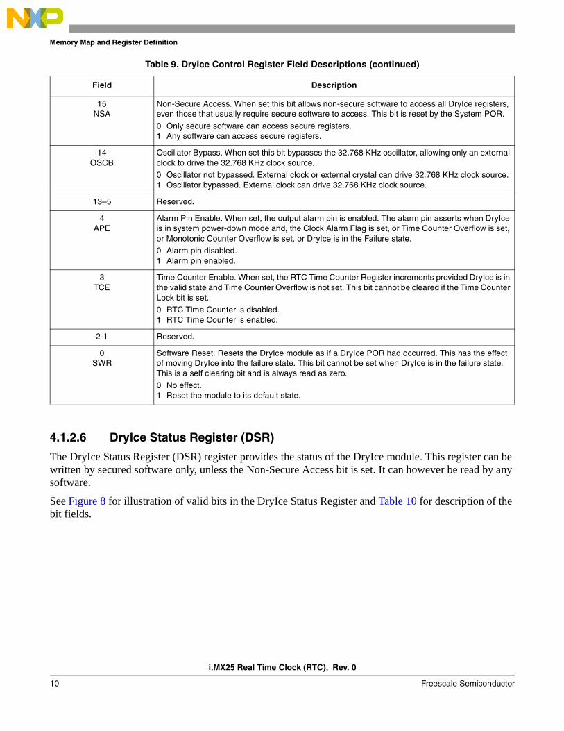
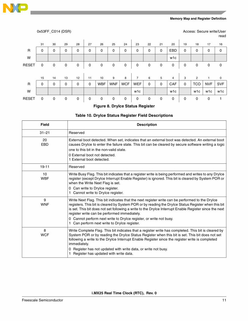
4.1.2.6 DryIce Status Register (DSR)
The DryIce Status Register (DSR) register provides the status of the DryIce module. This register can be written by secured software only, unless the Non-Secure Access bit is set. It can however be read by any software.
See Figure 8 for illustration of valid bits in the DryIce Status Register and Table 10 for description of the bit fields.
15NSA
Non-Secure Access. When set this bit allows non-secure software to access all DryIce registers, even those that usually require secure software to access. This bit is reset by the System POR.
0 Only secure software can access secure registers.1 Any software can access secure registers.
14OSCB
Oscillator Bypass. When set this bit bypasses the 32.768 KHz oscillator, allowing only an external clock to drive the 32.768 KHz clock source.
0 Oscillator not bypassed. External clock or external crystal can drive 32.768 KHz clock source.1 Oscillator bypassed. External clock can drive 32.768 KHz clock source.
13–5 Reserved.
4APE
Alarm Pin Enable. When set, the output alarm pin is enabled. The alarm pin asserts when DryIce is in system power-down mode and, the Clock Alarm Flag is set, or Time Counter Overflow is set, or Monotonic Counter Overflow is set, or DryIce is in the Failure state.
0 Alarm pin disabled.1 Alarm pin enabled.
3TCE
Time Counter Enable. When set, the RTC Time Counter Register increments provided DryIce is in the valid state and Time Counter Overflow is not set. This bit cannot be cleared if the Time Counter Lock bit is set.
0 RTC Time Counter is disabled.1 RTC Time Counter is enabled.
2-1 Reserved.
0SWR
Software Reset. Resets the DryIce module as if a DryIce POR had occurred. This has the effect of moving DryIce into the failure state. This bit cannot be set when DryIce is in the failure state. This is a self clearing bit and is always read as zero.
0 No effect.1 Reset the module to its default state.
Table 9. DryIce Control Register Field Descriptions (continued)
Field Description
i.MX25 Real Time Clock (RTC), Rev. 0
Freescale Semiconductor 11
Memory Map and Register Definition
0x53FF_C014 (DSR) Access: Secure write/Userread
31 30 29 28 27 26 25 24 23 22 21 20 19 18 17 16
R 0 0 0 0 0 0 0 0 0 0 0 EBD 0 0 0 0
W w1c
RESET 0 0 0 0 0 0 0 0 0 0 0 0 0 0 0 0
15 14 13 12 11 10 9 8 7 6 5 4 3 2 1 0
R 0 0 0 0 0 WBF WNF WCF WEF 0 0 CAF 0 TCO NVF SVF
W w1c w1c w1c w1c w1c
RESET 0 0 0 0 0 0 0 0 0 0 0 0 0 0 0 1
Figure 8. DryIce Status Register
Table 10. DryIce Status Register Field Descriptions
Field Description
31–21 Reserved
20EBD
External boot detected. When set, indicates that an external boot was detected. An external boot causes DryIce to enter the failure state. This bit can be cleared by secure software writing a logic
one to this bit in the non-valid state.
0 External boot not detected.1 External boot detected.
19-11 Reserved
10WBF
Write Busy Flag. This bit indicates that a register write is being performed and writes to any DryIce register (except DryIce Interrupt Enable Register) is ignored. This bit is cleared by System POR or when the Write Next Flag is set.
0 Can write to DryIce register.1 Cannot write to DryIce register.
9WNF
Write Next Flag. This bit indicates that the next register write can be performed to the DryIce registers. This bit is cleared by System POR or by reading the DryIce Status Register when this bit is set. This bit does not set following a write to the DryIce Interrupt Enable Register since the next register write can be performed immediately.
0 Cannot perform next write to DryIce register, or write not busy.1 Can perform next write to DryIce register.
8WCF
Write Complete Flag. This bit indicates that a register write has completed. This bit is cleared by System POR or by reading the DryIce Status Register when this bit is set. This bit does not set following a write to the DryIce Interrupt Enable Register since the register write is completed immediately.
0 Register has not updated with write data, or write not busy.1 Register has updated with write data.
i.MX25 Real Time Clock (RTC), Rev. 0
12 Freescale Semiconductor
Memory Map and Register Definition
4.1.2.7 DryIce Interrupt Enable Register (DIER)
The DryIce Interrupt Enable Register is used to enable and disable the DryIce interrupt sources. This register can only written by secured software, unless the Non-Secure Access bit is set. It can be read by any software.
See Figure 9 for illustration of valid bits in the DryIce Interrupt Enable Register and Table 11 for description of the bit fields.
7WEF
Write Error Flag. This bit indicates that a write to one of the registers was cancelled. This can be due to a write that occurs about the same time that DryIce is isolated or a write that occurs about the same time as a System POR. This bit can be cleared by secure software writing a logic one to this bit.
0 All writes completed.1 Write was cancelled.
6-5 Reserved
4CAF
Clock Alarm Flag. This bit sets when the 47-bit DryIce Time Counter Register increments to the value stored in the 47-bit DryIce Clock Alarm Register. This bit can be cleared by secure software writing a logic one to this bit.
0 Alarm has not occurred.1 Alarm has occurred.
3 Reserved
2TCO
Time Counter Overflow. When set, indicates that the Time Counter overflowed. This bit can be cleared by secure software writing a logic one to this bit provided DryIce is in the Valid or Non-Valid state.
0 Time Counter has not overflowed.1 Time Counter has overflowed.
1NVF
Non-Valid Flag. When set, indicates that DryIce is in the Non-Valid state. This bit sets if the Security Violation Flag is set during System POR and the Failure State Hard Lock bit is clear. This bit can be cleared by secure software writing a logic one to this bit.
0 DryIce is in the Valid or Failure state.1 DryIce is in the Non-Valid state.
0SVF
Security Violation Flag. When set, indicates that a security violation has been detected and DryIce has transitioned to the Failure state. If the Non-Valid Flag is also set (which happens following the next System POR), then DryIce has transitioned to the Non-Valid state. This bit can only be cleared if the Non-Valid Flag is set and by secure software writing a logic one to this bit, provided that the security violation is no longer present.
0 DryIce is in the Valid or Non-Valid state.1 Security violation has occurred and DryIce is in the Failure or Non-Valid state.
Table 10. DryIce Status Register Field Descriptions (continued)
Field Description

i.MX25 Real Time Clock (RTC), Rev. 0
Freescale Semiconductor 13
Memory Map and Register Definition
0x53FF_C018 (DIER) Access: Secure read/write
31 30 29 28 27 26 25 24 23 22 21 20 19 18 17 16
R 0 0 0 0 0 0 0 0 0 0 0 0 0 0 0 0
W
RESET 0 0 0 0 0 0 0 0 0 0 0 0 0 0 0 0
15 14 13 12 11 10 9 8 7 6 5 4 3 2 1 0
R 0 0 0 0 0 0WNIE WCIE WEIE
0 0CAIE
0TOIE
0 0
W
RESET 0 0 0 0 0 0 0 0 0 0 0 0 0 0 0 0
Figure 9. DryIce Interrupt Enable Register
Table 11. DryIce Interrupt Enable Register Field Descriptions
Field Description
31–10 Reserved.
9WNIE
Write Next Interrupt Enable. When set, this bit enables the Write Next Flag to generate a DryIce normal interrupt. This bit is reset by System POR.
0 Interrupt is disabled.1 Interrupt is enabled.
8WCIE
Write Complete Interrupt Enable. When set, this bit enables the Write Complete Flag to generate a DryIce normal interrupt. This bit is reset by System POR.
0 Interrupt is disabled.1 Interrupt is enabled.
7WEIE
Write Error Interrupt Enable. When set, this bit enables the Write Error Flag to generate a DryIce normal interrupt. This bit is reset by System POR.
0 Interrupt is disabled.1 Interrupt is enabled.
6-5 Reserved.
4CAIE
Clock Alarm Interrupt Enable. When set, this bit enables the Clock Alarm Flag to generate a DryIce normal interrupt. This bit is reset by System POR.
0 Interrupt is disabled.1 Interrupt is enabled.
3 Reserved
2TOIE
Time Overflow Interrupt Enable. When set, this bit enables the Time Counter Overflow status bit to generate a DryIce security interrupt. This bit is reset by System POR.
0 Interrupt is disabled.1 Interrupt is enabled.
1-0 Reserved.
i.MX25 Real Time Clock (RTC), Rev. 0
14 Freescale Semiconductor
Example
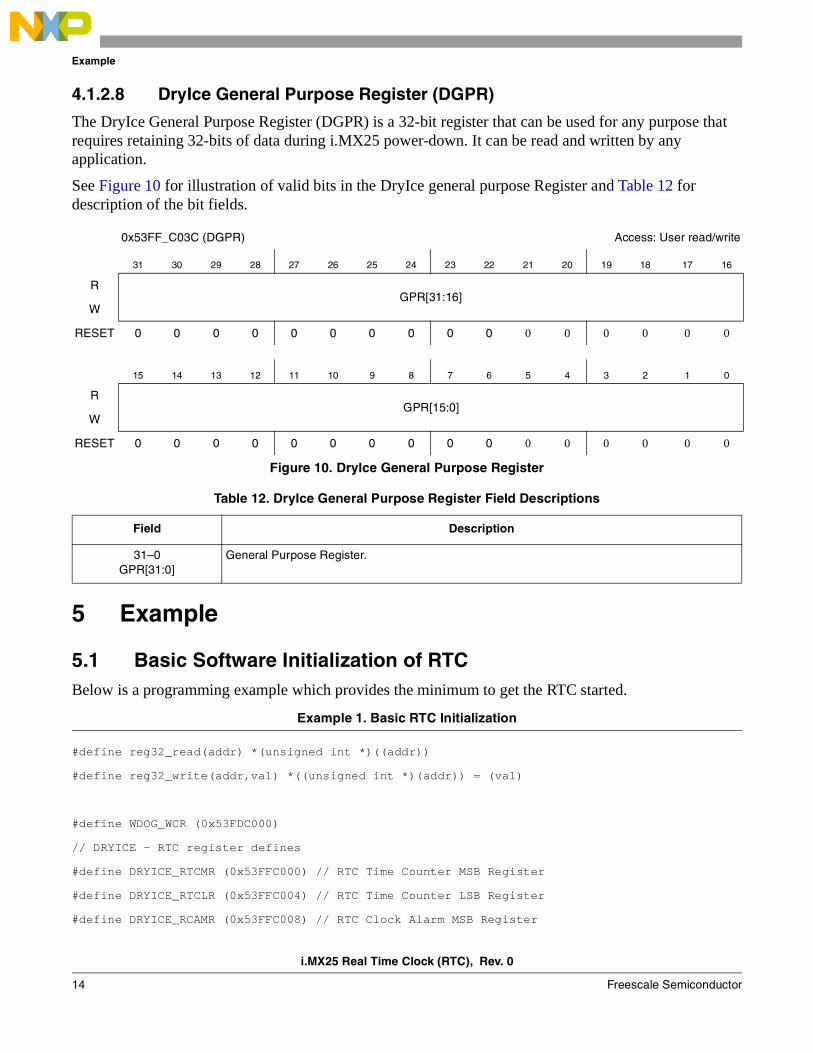
4.1.2.8 DryIce General Purpose Register (DGPR)
The DryIce General Purpose Register (DGPR) is a 32-bit register that can be used for any purpose that requires retaining 32-bits of data during i.MX25 power-down. It can be read and written by any application.
See Figure 10 for illustration of valid bits in the DryIce general purpose Register and Table 12 for description of the bit fields.
5 Example
5.1 Basic Software Initialization of RTCBelow is a programming example which provides the minimum to get the RTC started.
Example 1. Basic RTC Initialization
#define reg32_read(addr) *(unsigned int *)((addr))
#define reg32_write(addr,val) *((unsigned int *)(addr)) = (val)
#define WDOG_WCR (0x53FDC000)
// DRYICE - RTC register defines
#define DRYICE_RTCMR (0x53FFC000) // RTC Time Counter MSB Register
#define DRYICE_RTCLR (0x53FFC004) // RTC Time Counter LSB Register
#define DRYICE_RCAMR (0x53FFC008) // RTC Clock Alarm MSB Register
0x53FF_C03C (DGPR) Access: User read/write
31 30 29 28 27 26 25 24 23 22 21 20 19 18 17 16
RGPR[31:16]
W
RESET 0 0 0 0 0 0 0 0 0 0 0 0 0 0 0 0
15 14 13 12 11 10 9 8 7 6 5 4 3 2 1 0
RGPR[15:0]
W
RESET 0 0 0 0 0 0 0 0 0 0 0 0 0 0 0 0
Figure 10. DryIce General Purpose Register
Table 12. DryIce General Purpose Register Field Descriptions
Field Description
31–0GPR[31:0]
General Purpose Register.

i.MX25 Real Time Clock (RTC), Rev. 0
Freescale Semiconductor 15
Example
#define DRYICE_RCALR (0x53FFC00C) // RTC Clock Alarm LSB Register
#define DRYICE_DCR (0x53FFC010) // DryIce Control Register
#define DRYICE_DSR (0x53FFC014) // DryIce Status Register
#define DRYICE_DIER (0x53FFC018) // DryIce Interrupt Enable Register
#define DRYICE_DGPR (0x53FFC03C) // DryIce General Purpose Register
void reg32_dryice32kdomain_write(unsigned int addr , unsigned int wdata);
void main(void){
int i;
// Disable WDOG
*(unsigned short *)(WDOG_WCR) = 0x0030;
reg32_dryice32kdomain_write(DRYICE_DCR,0x8000); //disable security to allow any register writes
reg32_dryice32kdomain_write(DRYICE_DSR,0x03); // clear any security errors
reg32_dryice32kdomain_write(DRYICE_RTCMR,0x00); // need to write to the RTCMR to get RTC started
reg32_dryice32kdomain_write(DRYICE_DCR,0x8008); // enable the RTC
while(1); //you can now power down i.MX25 if you are supplying BAT_VDD and RTC will keep counting
}
//========Use the following to write to registers on 32kHz clock domain============
void reg32_dryice32kdomain_write(unsigned int addr , unsigned int wdata) {
unsigned int masked_wdata, rdata_tmp;
unsigned int dryice_status;
reg32_write(addr, wdata);
while ((reg32_read(DRYICE_DSR) & 0x200) != 0x200); // this line can be deleted if you are sure that previous 32kHz write operation has finished before this write.
while ((reg32_read(DRYICE_DSR) & 0x100) != 0x100);
reg32_read(DRYICE_DSR);
}

i.MX25 Real Time Clock (RTC), Rev. 0
16 Freescale Semiconductor
Revision History
5.2 Software RestrictionsDryIce has the following software restrictions:
• All DryIce register writes are committed on the third 32.768 KHz clock cycle following the peripheral bus write, except for the DryIce Interrupt Enable Register which takes effect immediately.
• The maximum throughput of register writes (except for DryIce Interrupt Enable Register) is one register write can complete every two 32.768 KHz clock cycles.
• All register write accesses complete with zero wait states due to the DryIce register interface. Subsequent writes are ignored if the Write Busy Flag is set.
• Register read accesses complete with either three or four wait states due to the DryIce register interface.
• All DryIce registers must be written using 32-bit operations, otherwise a bus error is generated.
• Attempting to read or write a DryIce register when DryIce is isolated generates a bus error.
5.3 BAT_VDDThe back-up power supply is powered through the BAT_VDD supply. The range for this supply can be set from 1.15 to 1.55 V. The typical drain on BAT_VDD is under 15 µA. Early characterization on a very small number of samples indicate this value to be much lower at room temperature (at around 6 µA), but a full characterization across a large sample still needs to be done.
There are a number of battery options users can choose from which are widely available on the market today. More specifically there is a wide range of silver oxide (low drain) micro-batteries which fit into the voltage range of BAT_VDD. Based on the mAh capacity of the battery and the low current consumption from BAT_VDD, some batteries are able maintain the RTC for a number of years.
6 Revision History Table 13 provides a revision history for this application note.
Table 13. Document Revision History
Rev.Number
Date Substantive Change(s)
0 06/2009 Initial release

i.MX25 Real Time Clock (RTC), Rev. 0
Freescale Semiconductor 17
Revision History
THIS PAGE INTENTIONALLY LEFT BLANK

i.MX25 Real Time Clock (RTC), Rev. 0
18 Freescale Semiconductor
Revision History
THIS PAGE INTENTIONALLY LEFT BLANK

i.MX25 Real Time Clock (RTC), Rev. 0
Freescale Semiconductor 19
Revision History
THIS PAGE INTENTIONALLY LEFT BLANK

Document Number: AN3874Rev. 006/2009
Information in this document is provided solely to enable system and software
implementers to use Freescale Semiconductor products. There are no express or
implied copyright licenses granted hereunder to design or fabricate any integrated
circuits or integrated circuits based on the information in this document.
Freescale Semiconductor reserves the right to make changes without further notice to
any products herein. Freescale Semiconductor makes no warranty, representation or
guarantee regarding the suitability of its products for any particular purpose, nor does
Freescale Semiconductor assume any liability arising out of the application or use of
any product or circuit, and specifically disclaims any and all liability, including without
limitation consequential or incidental damages. “Typical” parameters which may be
provided in Freescale Semiconductor data sheets and/or specifications can and do
vary in different applications and actual performance may vary over time. All operating
parameters, including “Typicals” must be validated for each customer application by
customer’s technical experts. Freescale Semiconductor does not convey any license
under its patent rights nor the rights of others. Freescale Semiconductor products are
not designed, intended, or authorized for use as components in systems intended for
surgical implant into the body, or other applications intended to support or sustain life,
or for any other application in which the failure of the Freescale Semiconductor product
could create a situation where personal injury or death may occur. Should Buyer
purchase or use Freescale Semiconductor products for any such unintended or
unauthorized application, Buyer shall indemnify and hold Freescale Semiconductor
and its officers, employees, subsidiaries, affiliates, and distributors harmless against all
claims, costs, damages, and expenses, and reasonable attorney fees arising out of,
directly or indirectly, any claim of personal injury or death associated with such
unintended or unauthorized use, even if such claim alleges that Freescale
Semiconductor was negligent regarding the design or manufacture of the part.
How to Reach Us:
Home Page: www.freescale.com
Web Support: http://www.freescale.com/support
USA/Europe or Locations Not Listed: Freescale Semiconductor, Inc.Technical Information Center, EL5162100 East Elliot Road Tempe, Arizona 85284 1-800-521-6274 or+1-480-768-2130www.freescale.com/support
Europe, Middle East, and Africa:Freescale Halbleiter Deutschland GmbHTechnical Information CenterSchatzbogen 781829 Muenchen, Germany+44 1296 380 456 (English) +46 8 52200080 (English)+49 89 92103 559 (German)+33 1 69 35 48 48 (French) www.freescale.com/support
Japan: Freescale Semiconductor Japan Ltd. HeadquartersARCO Tower 15F1-8-1, Shimo-Meguro, Meguro-ku Tokyo 153-0064Japan 0120 191014 or+81 3 5437 [email protected]
Asia/Pacific: Freescale Semiconductor China Ltd. Exchange Building 23FNo. 118 Jianguo RoadChaoyang DistrictBeijing 100022China+86 10 5879 [email protected]
For Literature Requests Only:Freescale Semiconductor
Literature Distribution Center P.O. Box 5405Denver, Colorado 80217 1-800 441-2447 or+1-303-675-2140Fax: +1-303-675-2150LDCForFreescaleSemiconductor
@hibbertgroup.com
Freescale and the Freescale logo are trademarks or registered trademarks of Freescale Semiconductor, Inc. in the U.S. and other countries. ARM is the registered trademark of ARM Limited. All other product or service names are the property of their respective owners.
© Freescale Semiconductor, Inc., 2009. All rights reserved.


