Download - Inel Dothan Proccesor

8/8/2019 Inel Dothan Proccesor
http://slidepdf.com/reader/full/inel-dothan-proccesor 1/65
Document Number: 316908-002
Intel ® P rocessor A100 and A110 on90 nm P rocess w ith 512-KB L2 CacheDatasheet
Ja n u a r y 2 0 0 8
8/8/2019 Inel Dothan Proccesor
http://slidepdf.com/reader/full/inel-dothan-proccesor 2/65
2 Datasheet
IINFORMATION IN THIS DOCUMENT IS PROVIDED IN CONNECTION WITH INTEL ® PRODUCTS. NO LICENSE, EXPRESS OR IMPLIED, BY ESTOPPEL OROTHERWISE, TO ANY INTELLECTUAL PROPERTY RIGHTS IS GRANTED BY THIS DOCUMENT. EXCEPT AS PROVIDED IN INTEL'S TERM S AND CONDITIONSOF SALE FOR SUCH PRODUCTS, INTEL ASSUMES NO LIABILITY WHATSOEVER, AND INTEL DISCLAIMS ANY EXPRESS OR IMPLIED WARRANTY, RELATINGTO SALE AND/OR USE OF INTEL PRODUCTS INCLUDING LIABILITY OR WARRANTIES RELATING TO FITNESS FOR A PARTICULAR PURPOSE,MERCHANTABILITY, OR INFRINGEMENT OF ANY PATENT, COPYRIGHT OR OTHER INTELLECTUAL PROPERTY RIGHT. Intel products are not intended foruse in medical, life saving, life sustaining applications.
Intel may make changes to specifications and product descriptions at any time, without notice.
Designers must not rely on the absence or characteristics of any features or instructions marked “reserved” or “undefined.” Intel reserves these forfuture definition and shall have no responsibility whatsoever for conflicts or incompatibilities arising from future changes to them.
The Intel ® Processor A100 and A110 on 90 nm process with 256-KB L2 cache may contain design defects or errors known as errata which m ay cause theproduct to deviate from published specifications. Current characterized errata are available on request.
Contact your local Intel sales office or your distributor to obtain the lat est specifications and before placing your product order.
Intel processor numbers are not a measure of performance. Processor numbers differentiate features within each processor family, not across differentprocessor families. See http://www.intel.com/products/processor_number for details. Over time processor numbers will incremen t based on changes inclock, speed, cache, FSB, or other features, and increments are not intended to represent proportional or quantitative increases in any particularfeature. Current roadmap processor number progression is not necessarily representative of future roadmaps. See www.intel.com/products/processor_number for details.
Intel ® 64 requires a computer system with a processor, chipset, BIOS, operating system, device drivers, and applications enabled for Intel 64. Processorwill not operate (including 32-bit operation) without an Intel 64-enabled BIOS. Performance will vary depending on your hardware and softwareconfigurations. Seehttp://www.intel.com/technology/intel64/index.htm for more information including details on which processors support Intel 64, orconsult with your system vendor for more information.
Enabling Execute Disable Bit functionality requires a PC with a processor with Execute Disable Bit capability and a supporting operating system. Checkwith your PC manufacturer on whether your system delivers Execute Disable Bit functionality.
Intel, Pentium, MMX, Intel SpeedStep and the Intel logo are trademarks of Intel Corporation in the U. S. and other countries.
*Other names and brands may be claimed as the property of others.
Copyright © 2007 - 2008, Intel Corporation. All rights reserved

8/8/2019 Inel Dothan Proccesor
http://slidepdf.com/reader/full/inel-dothan-proccesor 3/65
Datasheet 3
Contents
1 Introduction ..............................................................................................................71.1 Terminology ............................................... ................................................... ..... 81.2 References .........................................................................................................9
2 Low Pow er Features ................................................. ............................................... 112.1 Clock Control and Low Power States .................................................... ................ 11
2.1.1 Normal State ................................................ ......................................... 112.1.2 AutoHALT Power-Down State ............................................... .................... 112.1.3 Stop-Grant State.................... ................................................... ............. 122.1.4 HALT/Grant Snoop State ............................................. ............................ 122.1.5 Sleep State .................................................. ......................................... 122.1.6 Deep Sleep State ................................................. .................................. 132.1.7 Deeper Sleep State................................................................................. 13
2.2 Enhanced Intel SpeedStep® Technology ......................................................... ..... 142.3 Front Side Bus Low Power Enhancements ............................................................. 142.4 Processor Power Status Indicator (PSI#) Signal..................................................... 15
3 Electrical Specifications ............................................ ............................................... 173.1 Power and Ground Pins ................................................. ..................................... 17
3.1.1 FSB Clock (BCLK[1:0]) and Processor Clocking........................................... 173.2 Voltage Identification .................................................... ..................................... 173.3 Catastrophic Thermal Protection.......................................................................... 193.4 Signal Terminations and Unused Pins .................................................... ............... 193.5 FSB Frequency Select Signals (BSEL[1:0])............................................................ 193.6 FSB Signal Groups........................... ..................................................... ............. 193.7 CMOS Signals .............................................. .................................................... . 203.8 Maximum Ratings................. ..................................................... ........................ 213.9 Processor DC Specifications .................................................. .............................. 21
4 Package Mechanica l Spec if icat ions and Ba ll I n fo rmat ion ......................................... 274.1 Package Information....... ....................................................... ............................ 274.2 Processor Ballout............................................................................................... 294.3 Alphabetical Signals Reference .................................................... ........................ 50
5 Thermal Specifications and Design Considerations ......................................... ......... 595.1 Thermal Specifications .................................................. ..................................... 61
5.1.1 Thermal Diode .................................................. ..................................... 615.1.2 Thermal Diode Offset ................................................ .............................. 625.1.3 Intel ® Thermal Monitor..................................................... ...................... 63
8/8/2019 Inel Dothan Proccesor
http://slidepdf.com/reader/full/inel-dothan-proccesor 4/65
4 Datasheet
Figures1 Clock Control States .............................................. ................................................... 112 Active VCC and I CC Load Line for Processor...................................................................243 Deep Sleep V CC and I CC Load Line for Processor ................................................ ...........24
4 Micro-FCBGA Package ...............................................................................................285 Processor Ballout (Top View, Left Side)........................................................................306 Processor Ballout (top view, right side)........................................................................31
Tables1 References ............................................................................................................... 92 Voltage Identification Definition..................................................................................183 FSB Pin Groups ........................................................................................................204 Processor DC Absolute Maximum Ratings.....................................................................215 Voltage and Current Specifications (3 W processors) .....................................................226 Voltage and Current Specifications (5 W processors) .....................................................237 FSB Differential BCLK Specifications............................................................................258 AGTL+ Signal Group DC Specifications ........................................................................259 CMOS Signal Group DC Specifications..........................................................................2610 Open Drain Signal Group DC Specifications ..................................................................2611 Processor Ballout by Signal Name ...............................................................................3212 Processor Ballout by Ball Number ...............................................................................4113 Signal Description.....................................................................................................5014 Processor Power Specifications (3 W processors) ..........................................................6015 Processor Power Specifications (5 W processors) ..........................................................6116 Thermal Diode Interface ................................................... .........................................6217 Thermal Diode Specification .................................................. .....................................63

8/8/2019 Inel Dothan Proccesor
http://slidepdf.com/reader/full/inel-dothan-proccesor 5/65
Datasheet 5
Revision History
§ §
Revision Description Date
001 • Initial release April 2007
002 • Added a 5 W TDP version of the Intel ® Processor A110. January 2008

8/8/2019 Inel Dothan Proccesor
http://slidepdf.com/reader/full/inel-dothan-proccesor 6/65
6 Datasheet

8/8/2019 Inel Dothan Proccesor
http://slidepdf.com/reader/full/inel-dothan-proccesor 7/65
Datasheet 7
I n t r o d u c t i o n
1 I n t r o d u ct i o n
The Intel® Processors A100 and A110 are based on 90 nm process technologyfeaturing 512-KB L2 cache and 400-MHz front side bus (FSB). The processor is aderivative core based on the Intel® Pentium® M processor architecture that deliversperformance. The The Intel® Processors A100 and A110 are ultra low-power mobileprocessors.
N o t e : Throughout this document, the Intel Processors A100 and A110 on 90 nm process with512-KB L2 cache and 400 MHz FSB will be referred to as “processor”.
This document contains specifications for the Intel Processors A100 and A110.
The following list provides some of the key features on this processor:
• Supports Intel® Architecture with Dynamic Execution
• On-die, primary 32-KB instruction cache and 32-KB write-back data cache
• On-die, 512 KB second level cache with Advanced Transfer Cache Architecture• Way set associativity and ECC (Error Correcting Code) support
• Data Prefetch Logic
• Intel® Streaming SIMD Extensions 2 (Intel® SSE2)
• 400 MHz, source-synchronous FSB
• Advanced power management features including Enhanced Intel SpeedStep®technology
• Micro-FCBGA packaging technology
• Manufactured on Intel’s advanced 90 nanometer process technology with copperinterconnect.
• Support for MMX* technology and Internet Streaming SIMD instructions
• The processor’s data prefetch logic fetches data to the L2 cache before L1 cacherequests occurs, resulting in reduced bus cycle penalties and improvedperformance
• Micro-FCBGA packaging technology, including lead free SLI (second levelinterconnect) technology
• Execute Disable Bit support for enhanced security (available on processors withCPU Signature = 06D8h and recommended for implementation on Intel® 945GUExpress chipset family-based platforms only)
The processor is manufactured on Intel’s advanced 90 nm process technology withcopper interconnect. The processor maintains support for MMX technology and InternetStreaming SIMD instructions and full compatibility with IA-32 software. The on-die,32-KB Level 1 instruction and data caches along with the 512-KB L2 cache withadvanced transfer cache architecture enable significant performance improvement over
existing mobile processors. The processor’s data prefetch logic fetches data to the L2cache before L1 cache requests occurs, resulting in reduced bus cycle penalties andimproved performance.
The streaming Intel SSE2 enable break-through levels of performance in multimediaapplications including 3-D graphics, video decoding/encoding, and speech recognition.The new packed double-precision floating-point instructions enhance performance forapplications that require greater range and precision, including scientific andengineering applications and advanced 3-D geometry techniques, such as ray tracing.
8/8/2019 Inel Dothan Proccesor
http://slidepdf.com/reader/full/inel-dothan-proccesor 8/65
I n t r o d u c t i o n
8 Datasheet
The processor’s 400-MHz FSB uses a split-transaction, deferred reply protocol. The400-MHz FSB uses source-synchronous transfer (SST) of address and data to improveperformance by transferring data four times per bus clock (4X data transfer rate, as inAGP 4X). Along with the 4X data bus, the address bus can deliver addresses two timesper bus clock and is referred to as a “double-clocked” or 2X address bus. Working
together, the 4X data bus and 2X address bus provide a data bus bandwidth of up to3.2 GB/second. The FSB uses Advanced Gunning Transceiver Logic (AGTL+) signalingtechnology, a variant of GTL+ signaling technology with low power enhancements.
The processor features Enhanced Intel SpeedStep technology, which enables real-timedynamic switching between multiple voltage and frequency points. This results inoptimal performance without compromising low power. The processor features the AutoHalt, Stop Grant, Deep Sleep, and Deeper Sleep low power states.
The processor uses surface mount Micro Flip-Chip Ball Grid Array (Micro-FCBGA)package technology.
Intel Processors A100 and A110 with CPU Signature = 06D8h will also include theExecute Disable Bit capability. This feature combined with a support operating systemallows memory to be marked as executable or non executable. If code attempts to runin non-executable memory the processor raises an error to the operating system. Thisfeature can prevent some classes of viruses or worms that exploit buffer overrunvulnerabilities and can thus help improve the overall security of the system. See theIntel® Architecture Software Developer's Manual for more detailed information. Intelwill validate this feature only on Intel 945GU Express chipset family based platformsand recommends customers implement BIOS changes related to this feature, only onIntel 945GU Express chipset family based platforms.
N o t e : The term AGTL+ is used to refer to Assisted GTL+ signalling technology on some Intelprocessors.
1.1 Terminology
Term Definition
#
A “#” symbol after a signal name refers to an active low signal, indicating asignal is in the active state when driven to a low level. For example, whenRESET# is low, a reset has been requested. Conversely, when NMI is high,a nonmaskable interrupt has occurred. In the case of signals where thename does not imply an active state but describes part of a binarysequence (such as address or data ), the “#” symbol implies that the signalis inverted. For example, D[3:0] = “HLHL” refers to a hex ‘A’, and D[3:0]#= “LHLH” also refers to a hex “A” (H= High logic level, L= Low logic level).
Front Side Bus(FSB)
Refers to the interface between the processor and system core logic (alsoknown as the chipset components).

8/8/2019 Inel Dothan Proccesor
http://slidepdf.com/reader/full/inel-dothan-proccesor 9/65
Datasheet 9
I n t r o d u c t i o n
1.2 ReferencesMaterial and concepts available in the following documents may be beneficial whenreading this document.
§ §
Table 1. References
Document Document Number/Location
Intel ® Pentium ® M Processor on 90 nm Process with 2-MB L2 Cache - Specification Update
http://www.intel.com/design/mobile/specupdt/302209.htm
Mobile Intel ® 945 Express Chipset Family Datasheethttp://www.intel.com/design/mobile/datashts/309219.htm
Mobile Intel ® 945 Express Chipset Family Specification Updatehttp://www.intel.com/design/mobile/specupdt/309220.htm
Intel ® 64 and IA-32 Intel Architecture Software Developer's ManualVolume 1: Basic Architecture
http://www.intel.com/products/processor/manuals/
Volume 2A: Instruction Set Reference, A-M
Volume 2B: Instruction Set Reference, N-Z
Volume 3A: System Programming Guide
Volume 3B: System Programming Guide

8/8/2019 Inel Dothan Proccesor
http://slidepdf.com/reader/full/inel-dothan-proccesor 10/65
I n t r o d u c t i o n
10 Datasheet
8/8/2019 Inel Dothan Proccesor
http://slidepdf.com/reader/full/inel-dothan-proccesor 11/65
Datasheet 11
L o w P o w e r F ea t u r e s
2 Lo w Po w er Fea t u r es
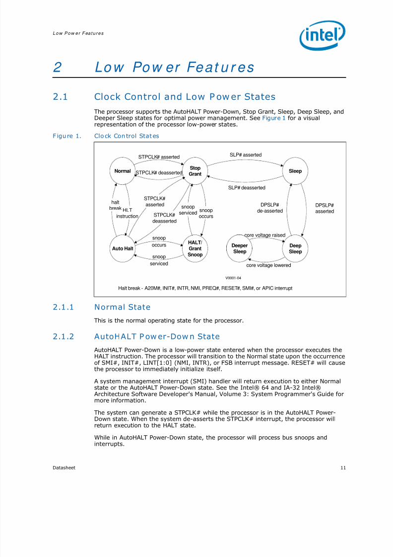
2.1 Clock Control and Low P ow er StatesThe processor supports the AutoHALT Power-Down, Stop Grant, Sleep, Deep Sleep, andDeeper Sleep states for optimal power management. See Figure 1 for a visualrepresentation of the processor low-power states.
2.1.1 Normal State
This is the normal operating state for the processor.
2.1.2 AutoHALT P ow er-Dow n State
AutoHALT Power-Down is a low-power state entered when the processor executes theHALT instruction. The processor will transition to the Normal state upon the occurrenceof SMI#, INIT#, LINT[1:0] (NMI, INTR), or FSB interrupt message. RESET# will causethe processor to immediately initialize itself.
A system management interrupt (SMI) handler will return execution to either Normal
state or the AutoHALT Power-Down state. See the Intel® 64 and IA-32 Intel®Architecture Software Developer's Manual, Volume 3: System Programmer's Guide formore information.
The system can generate a STPCLK# while the processor is in the AutoHALT Power-Down state. When the system de-asserts the STPCLK# interrupt, the processor willreturn execution to the HALT state.
While in AutoHALT Power-Down state, the processor will process bus snoops andinterrupts.
F igu re 1. Clo ck Con trol Stat es
snoopoccurs
StopGrantNormal Sleep
HALT/GrantSnoop
Auto Halt DeepSleep
STPCLK# asserted SLP# asserted
SLP# deasserted
STPCLK# deasserted
snoopserviced
HLTinstruction
snoopserviced snoop
occurs
DPSLP#de-asserted
DPSLP#asserted
STPCLK#asserted
STPCLK#deasserted
haltbreak
V0001-04
core voltage raised
core voltage lowered
Halt break - A20M#, INIT#, INTR, NMI, PREQ#, RESET#, SMI#, or APIC interrupt
DeeperSleep

8/8/2019 Inel Dothan Proccesor
http://slidepdf.com/reader/full/inel-dothan-proccesor 12/65
L o w P o w e r Fe a t u r e s
12 Datasheet
2.1.3 Stop-Grant State
When the STPCLK# pin is asserted, the Stop-Grant state of the processor is entered 20bus clocks after the response phase of the processor-issued Stop Grant Acknowledgespecial bus cycle.
Since the AGTL+ signal pins receive power from the FSB, these pins should not bedriven (allowing the level to return to V CCP ) for minimum power drawn by thetermination resistors in this state. In addition, all other input pins on the FSB should bedriven to the inactive state.
RESET# will cause the processor to immediately initialize itself, but the processor willstay in Stop-Grant state. A transition back to the Normal state will occur with the de-assertion of the STPCLK# signal. When re-entering the Stop-Grant state from the Sleepstate, STPCLK# should be de-asserted ten or more bus clocks after the de-assertion of SLP#.
A transition to the HALT/Grant Snoop state will occur when the processor detects asnoop on the FSB (see Section 2.1.3 ). A transition to the Sleep state (seeSection 2.1.5 ) will occur with the assertion of the SLP# signal.
While in the Stop-Grant State, SMI#, INIT# and LINT[1:0] will be latched by theprocessor, and only serviced when the processor returns to the Normal State. Only oneoccurrence of each event will be recognized upon return to the Normal state.
While in Stop-Grant state, the processor will process snoops on the FSB and it will latchinterrupts delivered on the FSB.
The PBE# signal can be driven when the processor is in Stop-Grant state. PBE# will beasserted if there is any pending interrupt latched within the processor. Pendinginterrupts that are blocked by the EFLAGS.IF bit being clear will still cause assertion of PBE#. Assertion of PBE# indicates to system logic that it should return the processor tothe Normal state.
2.1.4 HALT/ Grant Snoop State
The processor responds to snoop or interrupt transactions on the FSB while in Stop-Grant state or in AutoHALT Power-Down state. During a snoop or interrupt transaction,the processor enters the HALT/Grant Snoop state. The processor will stay in this stateuntil the snoop on the FSB has been serviced (whether by the processor or anotheragent on the FSB) or the interrupt has been latched. After the snoop is serviced or theinterrupt is latched, the processor will return to the Stop-Grant state or AutoHALTPower-Down state, as appropriate.
2.1.5 Sleep State
A low power state in which the processor maintains its context, maintains the phase-locked loop (PLL), and has stopped all internal clocks. The Sleep state can be enteredonly from Stop-Grant state. Once in the Stop-Grant state, the processor will enter theSleep state upon the assertion of the SLP# signal. The SLP# pin should only be
asserted when the processor is in the Stop Grant state. SLP# assertions while theprocessor is not in the Stop-Grant state is out of specification and may result inunapproved operation.
Snoop events that occur while in Sleep State or during a transition into or out of Sleepstate will cause unpredictable behavior.
8/8/2019 Inel Dothan Proccesor
http://slidepdf.com/reader/full/inel-dothan-proccesor 13/65
Datasheet 13
L o w P o w e r F ea t u r e s
In the Sleep state, the processor is incapable of responding to snoop transactions orlatching interrupt signals. No transitions or assertions of signals (with the exception of SLP#, DPSLP# or RESET#) are allowed on the FSB while the processor is in Sleepstate. Any transition on an input signal before the processor has returned to Stop-Grantstate will result in unpredictable behavior.
If RESET# is driven active while the processor is in the Sleep state, and held active asspecified in the RESET# pin specification, then the processor will reset itself, ignoringthe transition through Stop-Grant State. If RESET# is driven active while the processoris in the Sleep State, the SLP# and STPCLK# signals should be de-assertedimmediately after RESET# is asserted to ensure the processor correctly executes thereset sequence.
While in the Sleep state, the processor is capable of entering an even lower powerstate, the Deep Sleep state by asserting the DPSLP# pin (See Section 2.1.6 .). Whilethe processor is in the Sleep state, the SLP# pin must be de-asserted if anotherasynchronous FSB event needs to occur.
2.1.6 Deep Sleep State
Deep Sleep state is a very low power state the processor can enter while maintainingcontext. Deep Sleep state is entered by asserting the DPSLP# pin while in the Sleepstate. BCLK may be stopped during the Deep Sleep state for additional platform levelpower savings.
BCLK stop/restart timings on 945GU chipset-based platforms are as follows:
• Deep Sleep entry - DPSLP# and CPU_STP# are asserted simultaneously. Theplatform clock chip will stop/tristate BCLK within 2 BCLKs ± a few nanoseconds.
• Deep Sleep exit - DPSLP# and CPU_STP# are de-asserted simultaneously. Theplatform clock chip will drive BCLK to differential DC levels within 2-3 ns and startstoggling BCLK 2-6 BCLK periods later.
To re-enter the Sleep state, the DPSLP# pin must be de-asserted. BCLK can berestarted after DPSLP# de-assertion, as described above. A period of 30 microseconds(to allow for PLL stabilization) must occur before the processor can be considered to bein the Sleep State. Once in the Sleep state, the SLP# pin must be de-asserted to re-enter the Stop-Grant state.
While in Deep Sleep state, the processor is incapable of responding to snooptransactions or latching interrupt signals. No transitions of signals are allowed on theFSB while the processor is in Deep Sleep state. Any transition on an input signal beforethe processor has returned to Stop-Grant state will result in unpredictable behavior.
When the processor is in Deep Sleep state, it will not respond to interrupts or snooptransactions.
2.1.7 Deeper Sleep State
The Deeper Sleep state is the lowest power state the processor can enter. This state is
functionally identical to the Deep Sleep state but at a lower core voltage. The controlsignals to the voltage regulator to initiate a transition to the Deeper Sleep state areprovided on the platform.

8/8/2019 Inel Dothan Proccesor
http://slidepdf.com/reader/full/inel-dothan-proccesor 14/65
L o w P o w e r Fe a t u r e s
14 Datasheet
2.2 Enhanced Intel SpeedStep® TechnologyThe processor features Enhanced Intel SpeedStep technology. Unlike previousimplementations of Intel SpeedStep technology, this technology enables the processorto switch between multiple frequency and voltage points instead of two. This will enablesuperior performance with optimal power savings. Switching between states is softwarecontrolled unlike previous implementations where the GHI# pin is used to togglebetween two states. Following are the key features of Enhanced Intel SpeedSteptechnology:
• Multiple voltage/frequency operating points provide optimal performance at thelowest power.
• Voltage/Frequency selection is software controlled by writing to processor MSR’s(Model Specific Registers) thus eliminating chipset dependency.
— If the target frequency is higher than the current frequency, V CC is ramped upby placing a new value on the VID pins and the PLL then locks to the newfrequency.
— If the target frequency is lower than the current frequency, the PLL locks to thenew frequency and the V CC is changed through the VID pin mechanism.
— Software transitions are accepted at any time. If a previous transition is inprogress, the new transition is deferred until its completion.
• The processor controls voltage ramp rates internally to ensure glitch freetransitions.
• Low transition latency and large number of transitions possible per second.
— Processor core (including L2 cache) is unavailable for up to 10 μs during thefrequency transition
— The bus protocol (BNR# mechanism) is used to block snooping
• No bus master arbiter disable required prior to transition and no processor cacheflush necessary.
• Improved Intel ® Thermal Monitor mode.
— When the on-die thermal sensor indicates that the die temperature is too high,the processor can automatically perform a transition to a lower frequency/voltage specified in a software programmable MSR.
— The processor waits for a fixed time period. If the die temperature is down toacceptable levels, an up transition to the previous frequency/voltage pointoccurs.
— An interrupt is generated for the up and down Intel Thermal Monitor transitionsenabling better system level thermal management.
2.3 Front Side Bus Low P ow er EnhancementsThe processor incorporates the following front side bus (processor system bus) lowpower enhancements:
• Dynamic FSB Power Down• BPRI# control for address and control input buffers
• Dynamic On Die Termination disabling
• Low V CCP (I/O termination voltage)

8/8/2019 Inel Dothan Proccesor
http://slidepdf.com/reader/full/inel-dothan-proccesor 15/65
Datasheet 15
L o w P o w e r F ea t u r e s
The processor incorporates the DPWR# signal that controls the data bus input bufferson the processor. The DPWR# signal disables the buffers when not used and activatesthem only when data bus activity occurs, resulting in significant power savings with noperformance impact. BPRI# control also allows the processor address and control inputbuffers to be turned off when the BPRI# signal is inactive. The on-die termination on
the processor FSB buffers is disabled when the signals are driven low, resulting inadditional power savings. The low I/O termination voltage is on a dedicated voltageplane independent of the core voltage, enabling low I/O switching power at al l times.
2.4 P rocessor P ow er Status I ndicator ( PSI #) SignalThe processor incorporates the PSI# signal that is asserted when the processor is in alow power (Deep Sleep or Deeper Sleep) state. This signal is asserted upon Deep Sleepentry and de-asserted upon exit. PSI# can be used to improve the light load efficiencyof the voltage regulator, resulting in platform power savings and extended battery life.PSI# can also be used to simplify voltage regulator designs since it removes the needfor integrated 100 μs timers required to mask the PWRGOOD signal during DeeperSleep transitions. It also helps loosen PWRGOOD monitoring requirements in theDeeper Sleep state.
§ §

8/8/2019 Inel Dothan Proccesor
http://slidepdf.com/reader/full/inel-dothan-proccesor 16/65
L o w P o w e r Fe a t u r e s
16 Datasheet

8/8/2019 Inel Dothan Proccesor
http://slidepdf.com/reader/full/inel-dothan-proccesor 17/65
Datasheet 17
Elec t r i ca l Spec i f i ca t ion s
3 Elect r i ca l Sp eci f i ca t io n s
3.1 Pow er and Ground P insFor clean, on-chip power distribution, the processor has a large number of VCC (power)and VSS (ground) inputs. All power pins must be connected to V CC power planes whileall VSS pins must be connected to system ground planes. Use of multiple power andground planes is recommended to reduce I*R drop. The processor VCC pins must besupplied the voltage determined by the VID (Voltage ID) pins.
3 .1 .1 F SB Cl oc k ( BCL K[ 1:0 ]) an d P r oc es so r Cl oc ki ng
BCLK[1:0] directly controls the system bus interface speed as well as the corefrequency of the processor. As in previous generation processors, the Intel ProcessorA100 and A110 core frequency is a multiple of the BCLK[1:0] frequency. The processoruses a differential clocking implementation.
3.2 Voltage I dentificationThe processor uses six voltage identification pins, VID[5:0], to support automaticselection of power supply voltages. The VID pins for the processor are CMOS outputsdriven by the processor VID circuitry. Table 2 specifies the voltage level correspondingto the state of VID[5:0]. A “1” in this refers to a high-voltage level and a “0” refers tolow-voltage level.

8/8/2019 Inel Dothan Proccesor
http://slidepdf.com/reader/full/inel-dothan-proccesor 18/65
Elec t r i ca l Spec i f i ca t ion s
18 Datasheet
Tab le 2 . Vol ta ge I d en ti fi ca ti on D ef in it io n
VI D VCC(V )
VI D VCC(V )
5 4 3 2 1 0 5 4 3 2 1 00 0 1 0 0 0 1.580 1 0 0 1 0 0 1.132
0 0 1 0 0 1 1.564 1 0 0 1 0 1 1.116
0 0 1 0 1 0 1.548 1 0 0 1 1 0 1.100
0 0 1 0 1 1 1.532 1 0 0 1 1 1 1.084
0 0 1 1 0 0 1.516 1 0 1 0 0 0 1.068
0 0 1 1 0 1 1.500 1 0 1 0 0 1 1.052
0 0 1 1 1 0 1.484 1 0 1 0 1 0 1.036
0 0 1 1 1 1 1.468 1 0 1 0 1 1 1.020
0 1 0 0 0 0 1.452 1 0 1 1 0 0 1.004
0 1 0 0 0 1 1.436 1 0 1 1 0 1 0.9880 1 0 0 1 0 1.420 1 0 1 1 1 0 0.972
0 1 0 0 1 1 1.404 1 0 1 1 1 1 0.956
0 1 0 1 0 0 1.388 1 1 0 0 0 0 0.940
0 1 0 1 0 1 1.372 1 1 0 0 0 1 0.924
0 1 0 1 1 0 1.356 1 1 0 0 1 0 0.908
0 1 0 1 1 1 1.340 1 1 0 0 1 1 0.892
0 1 1 0 0 0 1.324 1 1 0 1 0 0 0.876
0 1 1 0 0 1 1.308 1 1 0 1 0 1 0.860
0 1 1 0 1 0 1.292 1 1 0 1 1 0 0.844
0 1 1 0 1 1 1.276 1 1 0 1 1 1 0.828
0 1 1 1 0 0 1.260 1 1 1 0 0 0 0.812
0 1 1 1 0 1 1.244 1 1 1 0 0 1 0.796
0 1 1 1 1 0 1.228 1 1 1 0 1 0 0.780
0 1 1 1 1 1 1.212 1 1 1 0 1 1 0.764
1 0 0 0 0 0 1.196 1 1 1 1 0 0 0.748
1 0 0 0 0 1 1.180 1 1 1 1 0 1 0.732
1 0 0 0 1 0 1.164 1 1 1 1 1 0 0.716
1 0 0 0 1 1 1.148 1 1 1 1 1 1 0.700
8/8/2019 Inel Dothan Proccesor
http://slidepdf.com/reader/full/inel-dothan-proccesor 19/65
Datasheet 19
Elec t r i ca l Spec i f i ca t ion s
3.3 Catastrophic Thermal P rotectionThe processor supports the THERMTRIP# signal for catastrophic thermal protection. Anexternal thermal sensor should also be used to protect the processor and the systemagainst excessive temperatures. Even with the activation of THERMTRIP#, which haltsall processor internal clocks and activity, leakage current can be high enough such thatthe processor cannot be protected in all conditions without the removal of power to theprocessor. If the external thermal sensor detects a catastrophic processor temperatureof 125°C (maximum), or if the THERMTRIP# signal is asserted, the V CC supply to theprocessor must be turned off within 500 ms to prevent permanent silicon damage dueto thermal runaway.
3.4 Signal Terminations and Unused P insAll RSVD (RESERVED) pins must remain unconnected. Connection of these pins to V CC,VSS , or to any other signal (including each other) can result in component malfunctionor incompatibility with future processors. See Section 4.2 for a pin listing of theprocessor and the location of all RSVD pins.
For reliable operation, always connect unused inputs or bidirectional signals to anappropriate signal level. Unused active low AGTL+ inputs may be left as no connects if AGTL+ termination is provided on the processor silicon. Unused active high inputsshould be connected through a resistor to ground (V SS ). Unused outputs can be leftunconnected.
For details on signal terminations, contact your Intel Field representative.
The TEST1 and TEST2 pins must have a stuffing option connection to V SS separately via1-k Ω, pull-down resistors.
3.5 FSB Frequency Select Signals (BSEL[ 1:0] )These signals are used to select the FSB clock frequency. They should be connected
between the processor and the chipset (G)MCH and clock generator on Intel 945GUExpress chipset family based platforms.
3.6 FSB Signal GroupsTo simplify the following discussion, the FSB signals have been combined into groupsby buffer type. AGTL+ input signals have differential input buffers, which use GTLREFas a reference level. In this document, the term "AGTL+ Input" refers to the AGTL+input group as well as the AGTL+ I/O group when receiving. Similarly, "AGTL+ Output"refers to the AGTL+ output group as well as the AGTL+ I/O group when driving.
With the implementation of a source synchronous data bus comes the need to specifytwo sets of timing parameters. One set is for common clock signals which aredependant upon the rising edge of BCLK0 (ADS#, HIT#, HITM#, etc.) and the second
set is for the source synchronous signals which are relative to their respective strobelines (data and address) as well as the rising edge of BCLK0. Asychronous signals arestill present (A20M#, IGNNE#, etc.) and can become active at any time during theclock cycle. Table 3 identifies which signals are common clock, source synchronous,and asynchronous.

8/8/2019 Inel Dothan Proccesor
http://slidepdf.com/reader/full/inel-dothan-proccesor 20/65
Elec t r i ca l Spec i f i ca t ion s
20 Datasheet
NOTES:1. Refer to Chapter 4 for signal descriptions and termination requirements.2. BPM[2:0}# and PRDY# are AGTL+ output only signals.3. In processor systems where there is no debug port implemented on the system board,
these signals are used to support a debug port interposer. In systems with the debug portimplemented on the system board, these signals are no connects.
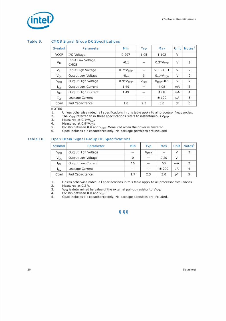
3.7 CMOS SignalsCMOS input signals are shown in Table 3 . Legacy output FERR#, IERR# and other non-AGTL+ signals (THERMTRIP# and PROCHOT#) use Open Drain output buffers. Thesesignals do not have setup or hold time specifications in relation to BCLK[1:0]. However,all of the CMOS signals are required to be asserted for at least three BCLKs in order forthe processor to recognize them. See Section 3.9 for the DC specifications for theCMOS signal groups.
Table 3. FSB P in Groups
Signal Group Type Signals 1
AGTL+ Common ClockInput Synchronousto BCLK[1:0] BPRI#, DEFER#, DPWR#, PREQ#, RESET#,RS[2:0]#, TRDY#
AGTL+ Common Clock I/O Synchronousto BCLK[1:0]
ADS#, BNR#, BPM[3:0]#, BR0#, DBSY#, DRDY#,HIT#, HITM#, LOCK#, PRDY#
AGTL+ SourceSynchronous I/O
Synchronousto assoc.strobe
AGTL+ Strobes Synchronousto BCLK[1:0] ADSTB[1:0]#, DSTBP[3:0]#, DSTBN[3:0]#
CMOS Input Asynchronous A20M#, DPSLP#, IGNNE#, INIT#, LINT0/INTR,LINT1/NMI, PWRGOOD, SMI#, SLP#, STPCLK#
Open Drain Output Asynchronous FERR#, IERR#, PROCHOT#, THERMTRIP#
CMOS Output Asynchronous PSI#, VID[5:0], BSEL[1:0]
CMOS Input Synchronousto TCK TCK, TDI, TMS, TRST#
Open Drain Output Synchronousto TCK TDO
FSB Clock Clock BCLK[1:0], ITP_CLK[1:0] 2
Power/OtherCOMP[3:0], DBR# 2 , GTLREF, RSVD, TEST2,TEST1, THERMDA, THERMDC, VCC, VCCA[3:0],VCCP, VCCQ[1:0], VCC_SENSE, VSS, VSS_SENSE
Signals Associated Strobe
REQ[4:0]#, A[16:3]# ADSTB[0]#
A[31:17]# ADSTB[1]#
D[15:0]#, DINV0# DSTBP0#, DSTBN0#
D[31:16]#, DINV1# DSTBP1#, DSTBN1#
D[47:32]#, DINV2# DSTBP2#, DSTBN2#
D[63:48]#, DINV3# DSTBP3#, DSTBN3#

8/8/2019 Inel Dothan Proccesor
http://slidepdf.com/reader/full/inel-dothan-proccesor 21/65
Datasheet 21
Elec t r i ca l Spec i f i ca t ion s
3.8 Maximum RatingsTable 4 lists the processor’s maximum environmental stress ratings. The processorshould not receive a clock while subjected to these conditions. Functional operatingparameters are listed in the DC tables. Extended exposure to the maximum ratingsmay affect device reliability. Furthermore, although the processor contains protectivecircuitry to resist damage from electro static discharge (ESD), one should always takeprecautions to avoid high static voltages or electric fields.
NOTES:1. This rating applies to any processor pin.2. Contact Intel for storage requirements in excess of one year.
3.9 Processor DC SpecificationsThe processor DC specifications in this section are defined at the processor core (pads)unless noted otherwise. See Table 4.3 for the pin signal definitions and signal pinassignments. The DC specifications for these signals are listed in Table 9 and Table 10 .
Table 5 through Table 10 list the DC specifications for the processor and are valid onlywhile meeting specifications for junction temperature, clock frequency, and inputvoltages. The Highest Frequency mode (HFM) and Lowest Frequency mode (LFM) referto the highest and lowest core operating frequencies supported on the processor. Activemode load line specifications apply in all states except in the Deep Sleep and DeeperSleep states. V CC,BOOT is the default voltage driven by the voltage regulator at powerup in order to set the VID values. Unless specified otherwise, all specifications for theprocessor are at Tjunction = 100°C. Care should be taken to read all notes associatedwith each parameter.
Tab le 4. P ro ce ss or DC A bs ol ut e M ax im um Ra ti ng s
Symbol Parameter Min Max Unit Notes
TSTORAGE Processor storage temperature -40 85 °C 2
VCCAny processor supply voltage withrespect to V SS
-0.3 1.6 V 1
VinAGTL+AGTL+ buffer DC input voltage withrespect to V SS
-0.1 1.6 V 1, 2
VinAsynch_CMOSCMOS buffer DC input voltage withrespect to V SS -0.1 1.6 V 1, 2

8/8/2019 Inel Dothan Proccesor
http://slidepdf.com/reader/full/inel-dothan-proccesor 22/65
Elec t r i ca l Spec i f i ca t ion s
22 Datasheet
NOTES:1. The voltage specifications are assumed to be measured at a via on the motherboard’s
opposite side of the processor’s socket (or BGA) ball with a 100-MHz bandwidthoscilloscope, 1.5-pF maximum probe capacitance, and 1-MOhms minimum impedance.The maximum length of ground wire on the probe should be less than 5 mm. Ensureexternal noise from the system is not coupled in the scope probe.
2. Specified at V CC,STATIC (nominal) under maximum signal loading conditions.3. Specified at the VID voltage.4. Based on simulations and averaged over the duration of any change in current. Specified
by design/characterization at nominal V CC. Not 100% tested.5. Measured at the bulk capacitors on the motherboard.6. Each processor is programmed with a maximum valid voltage identification value (VID),
which is set at manufacturing and can not be altered. Individual maximum VID values arecalibrated during manufacturing such that two processors at the same frequency may havedifferent settings within the VID range. Note that this differs from the VID employed by theprocessor during a power management event (Intel ® Thermal Monitor 2, Enhanced Intel ® SpeedStep Technology, or Enhanced Halt state).
Tab le 5 . Vol tage and Curr en t Spec if icat ions (3 W proces so rs )
Symbol Parameter Min Typ Max Unit Notes
VCCHFM VCC at Highest Frequency Mode (HFM) 0.796 — 0.94 V 6VCCLFM VCC at Lowest Frequency Mode (LFM) 0.796 — 0.94 V 6
VCC,BOOT Default V CC Voltage for Initial Power up 1.14 1.2 1.26 V 1
VCCP AGTL+ Termination Voltage 0.997 1.05 1.102 V 1
VCCA PLL Supply Voltage 1.425 1.5 1.575 V 1
VCCDPRSLP,TR Transient Deeper Sleep Voltage 0.669 0.726 0.783 V 1
VCCDPRSLP,ST Static Deeper Sleep Voltage 0.679 0.726 0.773 V 1
ICC 600 MHz & LFM V CC — — 4.5 A 2
800 MHz & HFM V CC — — 4.8 A
IAH, I SGNT ICC Auto-Halt & Stop-GrantHFM
LFM
— — 2.7
2.5
A 3
ISLP ICC SleepHFMLFM
— — 2.52.4
A 3
IDSLP ICC Deep SleepHFMLFM
— — 2.42.3
A 3
IDPRSLP ICC Deeper Sleep (C4) 0.7 V — — 2.0 A 3
dI CC/DT VCC Power Supply Current Slew Rate — — 0.5 A/ns 4, 5
ICCA ICC for V CCA Supply — — 120 mA
ICCP ICC for V CCP Supply — — 2.5 A
8/8/2019 Inel Dothan Proccesor
http://slidepdf.com/reader/full/inel-dothan-proccesor 23/65
Datasheet 23
Elec t r i ca l Spec i f i ca t ion s
NOTES:1. The voltage specifications are assumed to be measured at a via on the motherboard’s
opposite side of the processor’s socket (or BGA) ball with a 100-MHz bandwidthoscilloscope, 1.5-pF maximum probe capacitance, and 1-MOhms minimum impedance.The maximum length of ground wire on the probe should be less than 5 mm. Ensureexternal noise from the system is not coupled in the scope probe.
2. Specified at V CC,STATIC (nominal) under maximum signal loading conditions.3. Specified at the VID voltage.4. Based on simulations and averaged over the duration of any change in current. Specified
by design/characterization at nominal V CC . Not 100% tested.5. Measured at the bulk capacitors on the motherboard.6. Each processor is programmed with a maximum valid voltage identification value (VID),
which is set at manufacturing and can not be altered. Individual maximum VID values arecalibrated during manufacturing such that two processors at the same frequency may havedifferent settings within the VID range. Note that this differs from the VID employed by theprocessor during a power management event (Intel Thermal Monitor 2, Enhanced IntelSpeedStep Technology, or Enhanced Halt state).
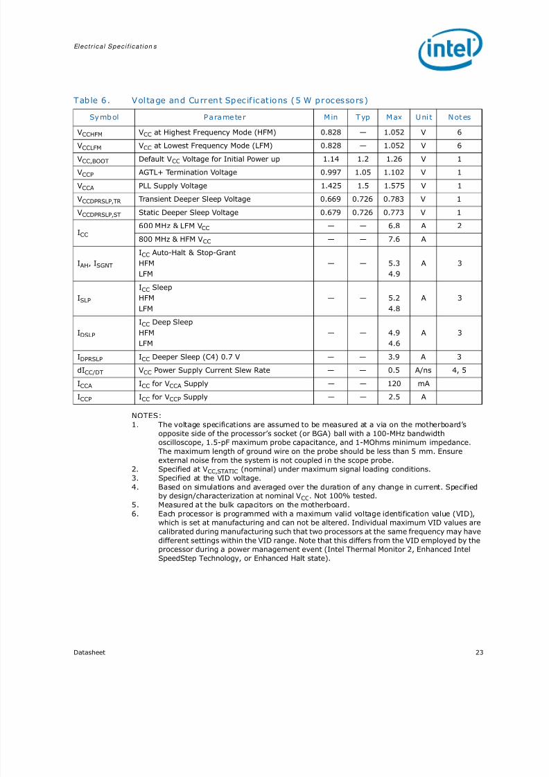
Tab le 6 . Vol tage and Curr en t Spec if icat ions (5 W p roces so rs )
Sy mb ol P a ra me te r M in Typ M ax U ni t N ot es
VCCHFM VCC at Highest Frequency Mode (HFM) 0.828 — 1.052 V 6VCCLFM VCC at Lowest Frequency Mode (LFM) 0.828 — 1.052 V 6
VCC,BOOT Default V CC Voltage for Initial Power up 1.14 1.2 1.26 V 1
VCCP AGTL+ Termination Voltage 0.997 1.05 1.102 V 1
VCCA PLL Supply Voltage 1.425 1.5 1.575 V 1
VCCDPRSLP,TR Transient Deeper Sleep Voltage 0.669 0.726 0.783 V 1
VCCDPRSLP,ST Static Deeper Sleep Voltage 0.679 0.726 0.773 V 1
ICC 600 MHz & LFM V CC — — 6.8 A 2
800 MHz & HFM V CC — — 7.6 A
IAH, I SGNT ICC Auto-Halt & Stop-GrantHFM
LFM
— — 5.3
4.9
A 3
ISLP ICC SleepHFMLFM
— — 5.24.8
A 3
IDSLP ICC Deep SleepHFMLFM
— — 4.94.6
A 3
IDPRSLP ICC Deeper Sleep (C4) 0.7 V — — 3.9 A 3
dI CC/DT VCC Power Supply Current Slew Rate — — 0.5 A/ns 4, 5
ICCA ICC for V CCA Supply — — 120 mA
ICCP ICC for V CCP Supply — — 2.5 A

8/8/2019 Inel Dothan Proccesor
http://slidepdf.com/reader/full/inel-dothan-proccesor 24/65
Elec t r i ca l Spec i f i ca t ion s
24 Datasheet
Figure 2. Active V CC and I CC Load Line for P rocessor
Figure 3. Deep Sleep V CC and I CC Load Line for P rocessor
ICC-CORE m ax{HFM|LFM}
VCC-CORE [V]
+/-1.5% from Nominal =VR Error
VCC-CORE, DC min {HFM|LFM}
VCC-CORE, DC max {HFM|LFM}
VCC-CORE max {HFM|LFM}
VCC-CORE min {HFM|LFM}
10mV= RIPPLE
0
Slope = -4.5mV/A at package
VCC-CORE nom {HFM|LFM}
ICC-CORE max
{HFM|LFM}
VCC-CORE [V]
+/-1.5% from Nominal =VR Error
VCC-CORE, DC min {HFM|LFM}
VCC-CORE, DC max {HFM|LFM}
VCC-CORE max {HFM|LFM}
VCC-CORE min {HFM|LFM}
10mV= RIPPLE
0
Slope = -4.5mV/A at package
VCC-CORE nom {HFM|LFM} – 1.2%
8/8/2019 Inel Dothan Proccesor
http://slidepdf.com/reader/full/inel-dothan-proccesor 25/65
Datasheet 25
Elec t r i ca l Spec i f i ca t ion s
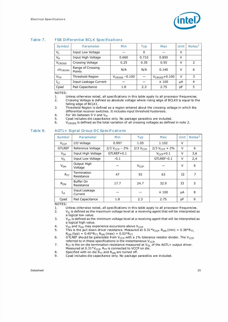
NOTES:1. Unless otherwise noted, all specifications in this table apply to all processor frequencies.2. Crossing Voltage is defined as absolute voltage where rising edge of BCLK0 is equal to the
falling edge of BCLK1.3. Threshold Region is defined as a region entered about the crossing voltage in which the
differential receiver switches. It includes input threshold hysteresis.4. For Vin between 0 V and V H.5. Cpad includes die capacitance only. No package parasitics are included.6. V CROSS is defined as the total variation of all crossing voltages as defined in note 2.
NOTES:1. Unless otherwise noted, all specifications in this table apply to all processor frequencies.2. V IL is defined as the maximum voltage level at a receiving agent that will be interpreted as
a logical low value.3. V IH is defined as the minimum voltage level at a receiving agent that will be interpreted as
a logical high value.4. V IH and V OH may experience excursions above V CCP.5. This is the pull down driver resistance. Measured at 0.31*V CCP. R ON (min) = 0.38*R TT,
RON (typ) = 0.45*R TT, RON (max) = 0.52*R TT.6. GTLREF should be generated from V CCP with a 1% tolerance resistor divider. The V CCP
referred to in these specifications is the instantaneous V CCP.7. R TT is the on-die termination resistance measured at V OL of the AGTL+ output driver.
Measured at 0.31*V CCP. R TT is connected to VCCP on die.8. Specified with on die R TT and R ON are turned off.9. Cpad includes die capacitance only. No package parasitics are included.
Tab le 7. F SB Di ff er en ti al BCL K Sp ec if ica ti on s
Symbol Parameter Min Typ Max Unit Notes 1
VL Input Low Voltage — 0 — V
VH Input High Voltage 0.660 0.710 0.850 V
VCROSS Crossing Voltage 0.25 0.35 0.55 V 2
ΔVCROSSRange of CrossingPoints N/A N/A 0.140 V 6
VTH Threshold Region V CROSS –0.100 — V CROSS +0.100 V 3
ILI Input Leakage Current — — ± 100 µA 4
Cpad Pad Capacitance 1.8 2.3 2.75 pF 5
Tab le 8. A GT L+ Si gn al Gr ou p D C Sp ec if ic at io ns
Symbol Parameter Min Typ Max Unit Notes 1
VCCP I/O Voltage 0.997 1.05 1.102 V
GTLREF Reference Voltage 2/3 V CCP – 2% 2/3 V CCP 2/3 V CCP + 2% V 6
VIH Input High Voltage GTLREF+0.1 V CCP +0.1 V 3,6
VIL Input Low Voltage -0.1 GTLREF–0.1 V 2,4
VOHOutput HighVoltage
— VCCP — V 6
RTTTerminationResistance 47 55 63 Ω 7
RONBuffer OnResistance 17.7 24.7 32.9 Ω 5
ILIInput LeakageCurrent — — ± 100 µA 8
Cpad Pad Capacitance 1.8 2.3 2.75 pF 9
8/8/2019 Inel Dothan Proccesor
http://slidepdf.com/reader/full/inel-dothan-proccesor 26/65
Elec t r i ca l Spec i f i ca t ion s
26 Datasheet
NOTES:
1. Unless otherwise noted, all specifications in this table apply to all processor frequencies.2. The V CCP referred to in these specifications refers to instantaneous V CCP.3. Measured at 0.1*V CCP.4. Measured at 0.9*V CCP.5. For Vin between 0 V and V CCP. Measured when the driver is tristated.6. Cpad includes die capacitance only. No package parasitics are included
1. Unless otherwise noted, all specifications in this table apply to all processor frequencies.2. Measured at 0.2 V.3. V OH is determined by value of the external pull-up resistor to V CCP.4. For Vin between 0 V and V OH .5. Cpad includes die capacitance only. No package parasitics are included.
§ § §
Tab le 9. CM OS Si gn al Gr ou p D C Sp ec if ic at io ns
Symbol Parameter Min Typ Max Unit Notes 1
VCCP I/O Voltage 0.997 1.05 1.102 V
VILInput Low VoltageCMOS
-0.1 — 0.3*V CCP V 2
VIH Input High Voltage 0.7*V CCP — VCCP+0.1 V 2
VOL Output Low Voltage -0.1 0 0.1*V CCP V 2
VOH Output High Voltage 0.9*V CCP VCCP VCCP +0.1 V 2
IOL Output Low Current 1.49 — 4.08 mA 3
IOH Output High Current 1.49 — 4.08 mA 4
ILI Leakage Current — — ± 100 µA 5
Cpad Pad Capacitance 1.0 2.3 3.0 pF 6
Table 10 . Open Drain Signal Group DC Specif ica tions
Symbol Parameter Min Typ Max Unit Notes 1
VOH Output High Voltage — V CCP — V 3
VOL Output Low Voltage 0 — 0.20 V
IOL Output Low Current 16 — 50 mA 2
I LO Leakage Current — — ± 200 µA 4Cpad Pad Capacitance 1.7 2.3 3.0 pF 5

8/8/2019 Inel Dothan Proccesor
http://slidepdf.com/reader/full/inel-dothan-proccesor 27/65
Datasheet 27
Package Mechan ica l Speci f i ca t io ns and Ba l l In fo rm a t ion
4 Pack ag e Mech an ica l Spec i f i ca t i on s and Ba l l I n f o r m a t i o n This chapter contains package mechanical specifications, ballout listing, and signaldescriptions.
4.1 Package InformationThe processor is available in a 663-ball, Micro-FCBGA package. The Micro-FCBGApackage may have capacitors placed in the area surrounding the die. Because the die-side capacitors are electrically conductive, and only slightly shorter than the die height,care should be taken to avoid contacting the capacitors with electrically conductivematerials. Doing so may short the capacitors, and possibly damage the device orrender it inactive. The use of an insulating material between the capacitors and anythermal solution should be considered to prevent capacitor shorting.
The mechanical drawing of the Micro-FCBGA package is shown in Figure 4 .

8/8/2019 Inel Dothan Proccesor
http://slidepdf.com/reader/full/inel-dothan-proccesor 28/65
Package Mechan ica l Spec i f i ca t ions and Ba l l In fo rm a t ion
28 Datasheet
F igu re 4 . M icro-F CBGA P ack age

8/8/2019 Inel Dothan Proccesor
http://slidepdf.com/reader/full/inel-dothan-proccesor 29/65
Datasheet 29
Package Mechan ica l Speci f i ca t io ns and Ba l l In fo rm a t ion
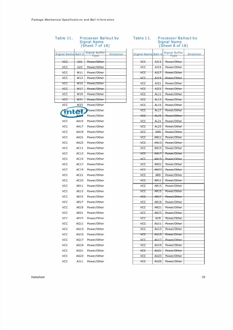
4.2 Processor BalloutFigure 5 and Figure 6 show the ballout from a top view of the package. Table 11 liststhe processor ballout by signal name. Table 12 lists the processor ballout by ballnumber.

8/8/2019 Inel Dothan Proccesor
http://slidepdf.com/reader/full/inel-dothan-proccesor 30/65
Package Mechan ica l Spec i f i ca t ions and Ba l l In fo rm a t ion
30 Datasheet
Figure 5 . P roces so r Bal lout (Top View, Lef t Side )1 2 3 4 5 6 7 8 9 10 11 12 13 14 15
A VSS SMI# SLP# DPSLP# BPM1# RSVD TCK A
B VSS VSS STPCLK# IERR# BPM0# RSVD TDI B
C VSS VCCSENSE VSS VSS VSS VSS VSS VSS C
D TEST1 VSSSENSE RSVD INIT# IGNNE# BPM2# RESET# D
E NMI VSS VSS RSVD A20M# RSVD BPM3# TMS E
F RSVD FERR# PWRGOOD VSS VSS VSS VSS F
G RSVD VSS VSS VSS VCCP VCCP VCCP VCCP G
H RSVD RSVD INTR VCCP VSS VSS VSS H
J RSVD VSS VSS VSS VCCP VCC VCC VCC J
K RSVD RSVD RSVD VCCP VSS VSS VSS K
L LOCK# VSS VSS VSS VCCP VCC VCC VCC L
M BPRI# RS0# RSVD VCCP VSS VSS VSS M
N RS1# VSS VSS VSS VCCP VCC VCC VCC N
P RS2# HIT# VCCP VCCP VSS VSS VSS P
R HITM# VSS VSS VSS VCCP VCC VCC VCC R
T DRDY# BNR# DBSY# VCCP VSS VSS VSS T
UDEFER
# VSS VSS VSS VCCP VCC VCC VCC U
V TRDY# BR0# RSVD VCCP VSS VSS VSS V
W ADS# VSS VSS VSS VCCP VCC VCC VCC W
Y REQ3# A6# RSVD VCCP VSS VSS VSS Y
AA REQ1# VSS VSS VSS VCCP VCC VCC VCC AA
AB A3# A9# A5# VCCP VSS VSS VSS AB
AC REQ0# VSS VSS VSS VCCP VCC VCC VCC AC
AD REQ4# A4# VCCQ1 VCCP VSS VSS VSS AD
AE REQ2# VSS VSS VSS VCCP VCC VCC VCC AE
AF ADSTB0# A14# COMP2 VCCP VSS VSS VSS AF
AG A13# VSS VSS VSS VCCP VCC VCC VCC AG
AH A10# A11# RSVD VCCP VSS VSS VSS AH
AJ A7# VSS VSS VSS VCCP VCC VCC VCC AJ
AK A8# A15# RSVD VCCP VSS VSS VSS AK
AL A12# VSS VSS VSS VCCP VCC VCC VCC AL
AM A16# COMP3 A24# RSVD VSS VSS VSS AM
AN A30# VSS VSS VSS VCC VCC VCC VCC AN
AP A23# A27# A18# RSVD VSS VSS VSS AP
AR A20# VSS VSS VSS VCC VCC VCC VCC AR
AT ADSTB1# A31# A25# RSVD VSS VSS VSS AT
AU A21# VSS VSS VSS VCC VCC VCC VCC AU
AV A26# A28# A19# RSVD VSS VSS VSS AV
AW A22# VSS VSS VSS VCC VCC VCC VCC AW
AY A29# A17# VID1 PSI# VSS VSS VSS AY
BA VSS VID4 VSS VSS VCC VCC VCC VCC BA
BB VSS VID5 VID2 RSVD VSS VSS VSS BB
BC VSS VID3 VID0 VCC VCC VCC VCC BC
1 2 3 4 5 6 7 8 9 10 11 12 13 14 15

8/8/2019 Inel Dothan Proccesor
http://slidepdf.com/reader/full/inel-dothan-proccesor 31/65
Datasheet 31
Package Mechan ica l Speci f i ca t io ns and Ba l l In fo rm a t ion
Figure 6 . P roces so r Bal lout ( top v iew, r ight si de )
16 17 18 19 20 21 22 23 24 25 26 27 28 29 30 31
A BSEL1 BCLK0 THERMDA D2# DSTBN0# D15# VSS A
B RSVD BCLK1 THERMDC D8# DSTBP0# D9# D12# VSS BC VSS VSS VSS VSS VSS VSS VSS VSS C
D TDO BSEL0 THERMTRIP# D0# D6# D4# RSVD D10# D
E TRST# PROCHOT# DPWR# D7# D3# RSVD VSS DINV0# E
F VSS VSS VSS VSS VSS VSS D5# D14# F
G VCCP VCCP VCCP VCCP VCCP D13# VSS D11# G
H VSS VSS VSS VSS VSS VSS D1# D21# H
J VCC VCC VCC VCC VCCP RSVD VSS D17# J
K VSS VSS VSS VSS VSS VSS RSVD D22# K
L VCC VCC VCC VCC VCCP TEST2 VSS D16# L
M VSS VSS VSS VSS VSS VSS VSS D20# M
N VCC VCC VCC VCC VCCP VCCA VSS D25# N
P VSS VSS VSS VSS VSS VSS D29# DSTBN1# P
R VCC VCC VCC VCC VCCP D23# VSS DSTBP1# R
T VSS VSS VSS VSS VSS VSS D18# DINV1# T
U VCC VCC VCC VCC VCCP D31# VSS D19# U
V VSS VSS VSS VSS VSS VSS D26# D24# V
W VCC VCC VCC VCC VCCP D28# VSS D30# W
Y VSS VSS VSS VSS VSS VSS COMP0 D27# Y
AA VCC VCC VCC VCC VCCP VCCQ0 VSS D38# AA
AB VSS VSS VSS VSS VSS VSS COMP1 D41# AB
AC VCC VCC VCC VCC VCCP D34# VSS D37# AC
AD VSS VSS VSS VSS VSS VSS D43# D39# AD
AE VCC VCC VCC VCC VCCP D42# VSS DINV2# AE
AF VSS VSS VSS VSS VSS VSS D32# D44# AF
AG VCC VCC VCC VCC VCCP D33# VSS DSTBN2# AG
AH VSS VSS VSS VSS VSS VSS D47# DSTBP2# AH
AJ VCC VCC VCC VCC VCCP GTLREF VSS D35# AJ
AK VSS VSS VSS VSS VSS VSS D40# D36# AK
AL VCC VCC VCC VCC VCCP RSVD VSS D46# AL
AM VSS VSS VSS VSS VSS VSS RSVD D45# AM
AN VCC VCC VCC VCC VCCP D56# VSS D50# AN
AP VSS VSS VSS VSS VSS VSS D52# D48# AP
AR VCC VCC VCC VCC VCCP D55# VSS D53# AR
AT VSS VSS VSS VSS VSS VSS D54# D57# AT
AU VCC VCC VCC VCC VCC D60# VSS D49# AU
AV VSS VSS VSS VSS VSS VSS D61# D63# AV
AW VCC VCC VCC VCC VCC D59# VSS DSTBP3# AW
AY VSS VSS VSS VSS VSS VSS D62# DSTBN3# AY
BA VCC VCC VCC VCC VCC D51# VSS VSS BA
BB VSS VSS VSS VSS VSS VSS DINV3# VSS BB
BC VCC VCC VCC VCC VCC D58# VSS BC
16 17 18 19 20 21 22 23 24 25 26 27 28 29 30 31

8/8/2019 Inel Dothan Proccesor
http://slidepdf.com/reader/full/inel-dothan-proccesor 32/65
Package Mechan ica l Spec i f i ca t ions and Ba l l In fo rm a t ion
32 Datasheet
Tab le 11 . P ro cess or Bal lo ut bySignal Name(Sheet 1 of 18)
Signal Name Ball # Signal BufferType Direction
A3# AB2 Source Synch Input/Output
A4# AD4 Source Synch Input/Output
A5# AB6 Source Synch Input/Output
A6# Y4 Source Synch Input/Output
A7# AJ1 Source Synch Input/Output
A8# AK2 Source Synch Input/Output
A9# AB4 Source Synch Input/Output
A10# AH2 Source Synch Input/Output
A11# AH4 Source Synch Input/Output
A12# AL1 Source Synch Input/Output
A13# AG1 Source Synch Input/OutputA14# AF4 Source Synch Input/Output
A15# AK4 Source Synch Input/Output
A16# AM2 Source Synch Input/Output
A17# AY4 Source Synch Input/Output
A18# AP6 Source Synch Input/Output
A19# AV6 Source Synch Input/Output
A20# AR1 Source Synch Input/Output
A21# AU1 Source Synch Input/Output
A22# AW1 Source Synch Input/Output
A23# AP2 Source Synch Input/Output
A24# AM6 Source Synch Input/Output
A25# AT6 Source Synch Input/Output
A26# AV2 Source Synch Input/Output
A27# AP4 Source Synch Input/Output
A28# AV4 Source Synch Input/Output
A29# AY2 Source Synch Input/Output
A30# AN1 Source Synch Input/Output
A31# AT4 Source Synch Input/Output
A20M# E9 CMOS Input
ADS# W1 Common Clock Input/Output
ADSTB0# AF2 Source Synch Input/Output
ADSTB1# AT2 Source Synch Input/Output
BCLK0 A19 Bus Clock Input
BCLK1 B18 Bus Clock Input
BNR# T4 Common Clock Input/Output
BPM0# B10 Common Clock Output
BPM1# A11 Common Clock Output
BPM2# D12 Common Clock Output
BPM3# E13 Common Clock Output
BPRI# M2 Common Clock Input
BR0# V4 Common Clock Input/Output
BSEL0 D18 CMOS Output
BSEL1 A17 CMOS Output
COMP0 Y28 Power/Other Input/Output
COMP1 AB28 Power/Other Input/Output
COMP2 AF6 Power/Other Input/Output
COMP3 AM4 Power/Other Input/Output
D0# D22 Source Synch Input/OutputD1# H28 Source Synch Input/Output
D2# A23 Source Synch Input/Output
D3# E25 Source Synch Input/Output
D4# D26 Source Synch Input/Output
D5# F28 Source Synch Input/Output
D6# D24 Source Synch Input/Output
D7# E23 Source Synch Input/Output
D8# B22 Source Synch Input/Output
D9# B26 Source Synch Input/Output
D10# D30 Source Synch Input/Output
D11# G31 Source Synch Input/Output
D12# B28 Source Synch Input/Output
D13# G27 Source Synch Input/Output
D14# F30 Source Synch Input/Output
D15# A27 Source Synch Input/Output
D16# L31 Source Synch Input/Output
D17# J31 Source Synch Input/Output
D18# T28 Source Synch Input/Output
D19# U31 Source Synch Input/Output
D20# M30 Source Synch Input/Output
D21# H30 Source Synch Input/Output
D22# K30 Source Synch Input/Output
D23# R27 Source Synch Input/Output
D24# V30 Source Synch Input/Output
D25# N31 Source Synch Input/Output
D26# V28 Source Synch Input/Output
D27# Y30 Source Synch Input/Output
Tabl e 11. P ro cesso r B al lo ut bySignal Name(Sheet 2 of 18)
Signal Name Ball # Signal BufferType Direction

8/8/2019 Inel Dothan Proccesor
http://slidepdf.com/reader/full/inel-dothan-proccesor 33/65
Package Mechan ica l Speci f i ca t io ns and Ba l l In fo rm a t ion
Datasheet 33
D28# W27 Source Synch Input/Output
D29# P28 Source Synch Input/Output
D30# W31 Source Synch Input/Output
D31# U27 Source Synch Input/Output
D32# AF28 Source Synch Input/Output
D33# AG27 Source Synch Input/Output
D34# AC27 Source Synch Input/Output
D35# AJ31 Source Synch Input/Output
D36# AK30 Source Synch Input/Output
D37# AC31 Source Synch Input/Output
D38# AA31 Source Synch Input/Output
D39# AD30 Source Synch Input/Output
D40# AK28 Source Synch Input/Output
D41# AB30 Source Synch Input/Output
D42# AE27 Source Synch Input/Output
D43# AD28 Source Synch Input/Output
D44# AF30 Source Synch Input/Output
D45# AM30 Source Synch Input/Output
D46# AL31 Source Synch Input/Output
D47# AH28 Source Synch Input/Output
D48# AP30 Source Synch Input/Output
D49# AU31 Source Synch Input/Output
D50# AN31 Source Synch Input/Output
D51# BA27 Source Synch Input/Output
D52# AP28 Source Synch Input/Output
D53# AR31 Source Synch Input/Output
D54# AT28 Source Synch Input/Output
D55# AR27 Source Synch Input/Output
D56# AN27 Source Synch Input/Output
D57# AT30 Source Synch Input/Output
D58# BC27 Source Synch Input/Output
D59# AW27 Source Synch Input/Output
D60# AU27 Source Synch Input/Output
D61# AV28 Source Synch Input/Output
D62# AY28 Source Synch Input/Output
D63# AV30 Source Synch Input/Output
DBSY# T6 Common Clock Input/Output
DEFER# U1 Common Clock Input
Tab le 11 . P roces sor Bal lou t bySignal Name(Sheet 3 of 18)
Signal Name Ball # Signal BufferType Direction
DINV0# E31 Source Synch Input/Output
DINV1# T30 CMOS Input/Output
DINV2# AE31 Source Synch Input/Output
DINV3# BB28 Source Synch Input/Output
DPSLP# A9 CMOS Input
DPWR# E21 Common Clock Input
DRDY# T2 Common Clock Input/Output
DSTBN0# A25 Source Synch Input/Output
DSTBN1# P30 Source Synch Input/Output
DSTBN2# AG31 Source Synch Input /Output
DSTBN3# AY30 Source Synch Input/Output
DSTBP0# B24 Source Synch Input/Output
DSTBP1# R31 Source Synch Input/Output
DSTBP2# AH30 Source Synch Input/Output
DSTBP3# AW31 Source Synch Input /Output
FERR# F4 Open Drain Output
GTLREF AJ27 Power/Other Input
HIT# P4 Common Clock Input/Output
HITM# R1 Common Clock Input/Output
IERR# B8 Open Drain Output
IGNNE# D10 CMOS Input
INIT# D8 CMOS Input
INTR H6
LOCK# L1 Common Clock Input/Output
NMI E1
PROCHOT# E19 Open Drain Output
PSI# AY8 CMOS Output
PWRGOOD F6 CMOS Input
REQ0# AC1 Source Synch Input/Output
REQ1# AA1 Source Synch Input/Output
REQ2# AE1 Source Synch Input/Output
REQ3# Y2 Source Synch Input/Output
REQ4# AD2 Source Synch Input/Output
RESET# D14 Common Clock Input
RS0# M4 Common Clock Input
RS1# N1 Common Clock Input
RS2# P2 Common Clock Input
RSVD A13 Reserved
Tabl e 11. P ro cesso r Ba ll ou t b ySignal Name(Sheet 4 of 18)
Signal Name Ball # Signal BufferType Direction

8/8/2019 Inel Dothan Proccesor
http://slidepdf.com/reader/full/inel-dothan-proccesor 34/65
Package Mechan ica l Spec i f i ca t ions and Ba l l In fo rm a t ion
34 Datasheet
RSVD B12 Reserved
RSVD B16 Reserved
RSVD D6 Reserved
RSVD D28 Reserved
RSVD E7 Reserved
RSVD E11 Reserved
RSVD E27 Reserved
RSVD F2 Reserved
RSVD G1 Reserved
RSVD H2 Reserved
RSVD H4 ReservedRSVD J1 Reserved
RSVD J27 Reserved
RSVD K2 Reserved
RSVD K4 Reserved
RSVD K6 Reserved
RSVD K28 Reserved
RSVD M6 Reserved
RSVD V6 Reserved
RSVD Y6 Reserved
RSVD AH6 Reserved
RSVD AK6 Reserved
RSVD AL27 Reserved
RSVD AM8 Reserved
RSVD AM28 Reserved
RSVD AP8 Reserved
RSVD AT8 Reserved
RSVD AV8 Reserved
RSVD BB8 Reserved
SLP# A7 CMOS Input
SMI# A5 CMOS Input
STPCLK# B6 CMOS Input
TCK A15 CMOS Input
TDI B14 CMOS Input
TDO D16 Open Drain Output
TEST1 D2 Test
TEST2 L27 Test
THERMDA A21 Power/Other
Tab le 11 . P ro cess or Bal lo ut bySignal Name(Sheet 5 of 18)
Signal Name Ball # Signal BufferType Direction
THERMDC B20 Power/Other
THERMTRIP# D20 Open Drain Output
TMS E15 CMOS Input
TRDY# V2 Common Clock Input
TRST# E17 CMOS Input
VCC J11 Power/Other
VCC J13 Power/Other
VCC J15 Power/Other
VCC J17 Power/Other
VCC J19 Power/Other
VCC J21 Power/OtherVCC J23 Power/Other
VCC L11 Power/Other
VCC L13 Power/Other
VCC L15 Power/Other
VCC L17 Power/Other
VCC L19 Power/Other
VCC L21 Power/Other
VCC L23 Power/Other
VCC N11 Power/Other
VCC N13 Power/Other
VCC N15 Power/Other
VCC N17 Power/Other
VCC N19 Power/Other
VCC N21 Power/Other
VCC N23 Power/Other
VCC R11 Power/Other
VCC R13 Power/Other
VCC R15 Power/Other
VCC R17 Power/Other
VCC R19 Power/Other
VCC R21 Power/Other
VCC R23 Power/Other
VCC U11 Power/Other
VCC U13 Power/Other
VCC U15 Power/Other
VCC U17 Power/Other
VCC U19 Power/Other
Tabl e 11. P ro cesso r B al lo ut bySignal Name(Sheet 6 of 18)
Signal Name Ball # Signal BufferType Direction
8/8/2019 Inel Dothan Proccesor
http://slidepdf.com/reader/full/inel-dothan-proccesor 35/65
Package Mechan ica l Speci f i ca t io ns and Ba l l In fo rm a t ion
Datasheet 35
VCC U21 Power/Other
VCC U23 Power/Other
VCC W11 Power/Other
VCC W13 Power/Other
VCC W15 Power/Other
VCC W17 Power/Other
VCC W19 Power/Other
VCC W21 Power/Other
VCC W23 Power/Other
VCC AA11 Power/Other
VCC AA13 Power/Other
VCC AA15 Power/Other
VCC AA17 Power/Other
VCC AA19 Power/Other
VCC AA21 Power/Other
VCC AA23 Power/Other
VCC AC11 Power/Other
VCC AC13 Power/Other
VCC AC15 Power/Other
VCC AC17 Power/Other
VCC AC19 Power/Other
VCC AC21 Power/Other
VCC AC23 Power/Other
VCC AE11 Power/Other
VCC AE13 Power/Other
VCC AE15 Power/Other
VCC AE17 Power/Other
VCC AE19 Power/Other
VCC AE21 Power/Other
VCC AE23 Power/Other
VCC AG11 Power/Other
VCC AG13 Power/Other
VCC AG15 Power/Other
VCC AG17 Power/Other
VCC AG19 Power/Other
VCC AG21 Power/Other
VCC AG23 Power/Other
VCC AJ11 Power/Other
Tab le 11 . P roces sor Bal lou t bySignal Name(Sheet 7 of 18)
Signal Name Ball # Signal BufferType Direction
VCC AJ13 Power/Other
VCC AJ15 Power/Other
VCC AJ17 Power/Other
VCC AJ19 Power/Other
VCC AJ21 Power/Other
VCC AJ23 Power/Other
VCC AL11 Power/Other
VCC AL13 Power/Other
VCC AL15 Power/Other
VCC AL17 Power/Other
VCC AL19 Power/Other
VCC AL21 Power/Other
VCC AL23 Power/Other
VCC AN9 Power/Other
VCC AN11 Power/Other
VCC AN13 Power/Other
VCC AN15 Power/Other
VCC AN17 Power/Other
VCC AN19 Power/Other
VCC AN21 Power/Other
VCC AN23 Power/Other
VCC AR9 Power/Other
VCC AR11 Power/Other
VCC AR13 Power/Other
VCC AR15 Power/Other
VCC AR17 Power/Other
VCC AR19 Power/Other
VCC AR21 Power/Other
VCC AR23 Power/Other
VCC AU9 Power/Other
VCC AU11 Power/Other
VCC AU13 Power/Other
VCC AU15 Power/Other
VCC AU17 Power/Other
VCC AU19 Power/Other
VCC AU21 Power/Other
VCC AU23 Power/Other
VCC AU25 Power/Other
Tabl e 11. P ro cesso r Ba ll ou t b ySignal Name(Sheet 8 of 18)
Signal Name Ball # Signal BufferType Direction

8/8/2019 Inel Dothan Proccesor
http://slidepdf.com/reader/full/inel-dothan-proccesor 36/65
Package Mechan ica l Spec i f i ca t ions and Ba l l In fo rm a t ion
36 Datasheet
VCC AW9 Power/Other
VCC AW11 Power/Other
VCC AW13 Power/Other
VCC AW15 Power/Other
VCC AW17 Power/Other
VCC AW19 Power/Other
VCC AW21 Power/Other
VCC AW23 Power/Other
VCC AW25 Power/Other
VCC BA9 Power/Other
VCC BA11 Power/OtherVCC BA13 Power/Other
VCC BA15 Power/Other
VCC BA17 Power/Other
VCC BA19 Power/Other
VCC BA21 Power/Other
VCC BA23 Power/Other
VCC BA25 Power/Other
VCC BC9 Power/Other
VCC BC11 Power/Other
VCC BC13 Power/Other
VCC BC15 Power/Other
VCC BC17 Power/Other
VCC BC19 Power/Other
VCC BC21 Power/Other
VCC BC23 Power/Other
VCC BC25 Power/Other
VCCA N27 Power/Other
VCCP G9 Power/Other
VCCP G11 Power/Other
VCCP G13 Power/Other
VCCP G15 Power/Other
VCCP G17 Power/Other
VCCP G19 Power/Other
VCCP G21 Power/Other
VCCP G23 Power/Other
VCCP G25 Power/Other
VCCP H8 Power/Other
Tab le 11 . P ro cess or Bal lo ut bySignal Name(Sheet 9 of 18)
Signal Name Ball # Signal BufferType Direction
VCCP J9 Power/Other
VCCP J25 Power/Other
VCCP K8 Power/Other
VCCP L9 Power/Other
VCCP L25 Power/Other
VCCP M8 Power/Other
VCCP N9 Power/Other
VCCP N25 Power/Other
VCCP P6 Power/Other
VCCP P8 Power/Other
VCCP R9 Power/OtherVCCP R25 Power/Other
VCCP T8 Power/Other
VCCP U9 Power/Other
VCCP U25 Power/Other
VCCP V8 Power/Other
VCCP W9 Power/Other
VCCP W25 Power/Other
VCCP Y8 Power/Other
VCCP AA9 Power/Other
VCCP AA25 Power/Other
VCCP AB8 Power/Other
VCCP AC9 Power/Other
VCCP AC25 Power/Other
VCCP AD8 Power/Other
VCCP AE9 Power/Other
VCCP AE25 Power/Other
VCCP AF8 Power/Other
VCCP AG9 Power/Other
VCCP AG25 Power/Other
VCCP AH8 Power/Other
VCCP AJ9 Power/Other
VCCP AJ25 Power/Other
VCCP AK8 Power/Other
VCCP AL9 Power/Other
VCCP AL25 Power/Other
VCCP AN25 Power/Other
VCCP AR25 Power/Other
Tabl e 11. P ro cesso r B al lo ut bySignal Name(Sheet 10 of 18)
Signal Name Ball # Signal BufferType Direction

8/8/2019 Inel Dothan Proccesor
http://slidepdf.com/reader/full/inel-dothan-proccesor 37/65
Package Mechan ica l Speci f i ca t io ns and Ba l l In fo rm a t ion
Datasheet 37
VCCQ0 AA27 Power/Other
VCCQ1 AD6 Power/Other
VCCSENSE C3 Power/Other Output
VID0 BC7 CMOS Output
VID1 AY6 CMOS Output
VID2 BB6 CMOS Output
VID3 BC5 CMOS Output
VID4 BA3 CMOS Output
VID5 BB4 CMOS Output
VSS A3 Power/Other
VSS A29 Power/Other
VSS B2 Power/Other
VSS B4 Power/Other
VSS B30 Power/Other
VSS C1 Power/Other
VSS C5 Power/Other
VSS C7 Power/Other
VSS C9 Power/Other
VSS C11 Power/Other
VSS C13 Power/Other
VSS C15 Power/Other
VSS C17 Power/Other
VSS C19 Power/Other
VSS C21 Power/Other
VSS C23 Power/Other
VSS C25 Power/Other
VSS C27 Power/Other
VSS C29 Power/Other
VSS C31 Power/Other
VSS E3 Power/Other
VSS E5 Power/Other
VSS E29 Power/Other
VSS F8 Power/Other
VSS F10 Power/Other
VSS F12 Power/Other
VSS F14 Power/Other
VSS F16 Power/Other
VSS F18 Power/Other
Tab le 11 . P roces sor Bal lou t bySignal Name(Sheet 11 of 18)
Signal Name Ball # Signal BufferType Direction
VSS F20 Power/Other
VSS F22 Power/Other
VSS F24 Power/Other
VSS F26 Power/Other
VSS G3 Power/Other
VSS G5 Power/Other
VSS G7 Power/Other
VSS G29 Power/Other
VSS H10 Power/Other
VSS H12 Power/Other
VSS H14 Power/Other
VSS H16 Power/Other
VSS H18 Power/Other
VSS H20 Power/Other
VSS H22 Power/Other
VSS H24 Power/Other
VSS H26 Power/Other
VSS J3 Power/Other
VSS J5 Power/Other
VSS J7 Power/Other
VSS J29 Power/Other
VSS K10 Power/Other
VSS K12 Power/Other
VSS K14 Power/Other
VSS K16 Power/Other
VSS K18 Power/Other
VSS K20 Power/Other
VSS K22 Power/Other
VSS K24 Power/Other
VSS K26 Power/Other
VSS L3 Power/Other
VSS L5 Power/Other
VSS L7 Power/Other
VSS L29 Power/Other
VSS M10 Power/Other
VSS M12 Power/Other
VSS M14 Power/Other
VSS M16 Power/Other
Tabl e 11. P ro cesso r Ba ll ou t b ySignal Name(Sheet 12 of 18)
Signal Name Ball # Signal BufferType Direction

8/8/2019 Inel Dothan Proccesor
http://slidepdf.com/reader/full/inel-dothan-proccesor 38/65
Package Mechan ica l Spec i f i ca t ions and Ba l l In fo rm a t ion
38 Datasheet
VSS M18 Power/Other
VSS M20 Power/Other
VSS M22 Power/Other
VSS M24 Power/Other
VSS M26 Power/Other
VSS M28 Power/Other
VSS N3 Power/Other
VSS N5 Power/Other
VSS N7 Power/Other
VSS N29 Power/Other
VSS P10 Power/OtherVSS P12 Power/Other
VSS P14 Power/Other
VSS P16 Power/Other
VSS P18 Power/Other
VSS P20 Power/Other
VSS P22 Power/Other
VSS P24 Power/Other
VSS P26 Power/Other
VSS R3 Power/Other
VSS R5 Power/Other
VSS R7 Power/Other
VSS R29 Power/Other
VSS T10 Power/Other
VSS T12 Power/Other
VSS T14 Power/Other
VSS T16 Power/Other
VSS T18 Power/Other
VSS T20 Power/Other
VSS T22 Power/Other
VSS T24 Power/Other
VSS T26 Power/Other
VSS U3 Power/Other
VSS U5 Power/Other
VSS U7 Power/Other
VSS U29 Power/Other
VSS V10 Power/Other
VSS V12 Power/Other
Tab le 11 . P ro cess or Bal lo ut bySignal Name(Sheet 13 of 18)
Signal Name Ball # Signal BufferType Direction
VSS V14 Power/Other
VSS V16 Power/Other
VSS V18 Power/Other
VSS V20 Power/Other
VSS V22 Power/Other
VSS V24 Power/Other
VSS V26 Power/Other
VSS W3 Power/Other
VSS W5 Power/Other
VSS W7 Power/Other
VSS W29 Power/OtherVSS Y10 Power/Other
VSS Y12 Power/Other
VSS Y14 Power/Other
VSS Y16 Power/Other
VSS Y18 Power/Other
VSS Y20 Power/Other
VSS Y22 Power/Other
VSS Y24 Power/Other
VSS Y26 Power/Other
VSS AA3 Power/Other
VSS AA5 Power/Other
VSS AA7 Power/Other
VSS AA29 Power/Other
VSS AB10 Power/Other
VSS AB12 Power/Other
VSS AB14 Power/Other
VSS AB16 Power/Other
VSS AB18 Power/Other
VSS AB20 Power/Other
VSS AB22 Power/Other
VSS AB24 Power/Other
VSS AB26 Power/Other
VSS AC3 Power/Other
VSS AC5 Power/Other
VSS AC7 Power/Other
VSS AC29 Power/Other
VSS AD10 Power/Other
Tabl e 11. P ro cesso r B al lo ut bySignal Name(Sheet 14 of 18)
Signal Name Ball # Signal BufferType Direction

8/8/2019 Inel Dothan Proccesor
http://slidepdf.com/reader/full/inel-dothan-proccesor 39/65
Package Mechan ica l Speci f i ca t io ns and Ba l l In fo rm a t ion
Datasheet 39
VSS AD12 Power/Other
VSS AD14 Power/Other
VSS AD16 Power/Other
VSS AD18 Power/Other
VSS AD20 Power/Other
VSS AD22 Power/Other
VSS AD24 Power/Other
VSS AD26 Power/Other
VSS AE3 Power/Other
VSS AE5 Power/Other
VSS AE7 Power/Other
VSS AE29 Power/Other
VSS AF10 Power/Other
VSS AF12 Power/Other
VSS AF14 Power/Other
VSS AF16 Power/Other
VSS AF18 Power/Other
VSS AF20 Power/Other
VSS AF22 Power/Other
VSS AF24 Power/Other
VSS AF26 Power/Other
VSS AG3 Power/Other
VSS AG5 Power/Other
VSS AG7 Power/Other
VSS AG29 Power/Other
VSS AH10 Power/Other
VSS AH12 Power/Other
VSS AH14 Power/Other
VSS AH16 Power/Other
VSS AH18 Power/Other
VSS AH20 Power/Other
VSS AH22 Power/Other
VSS AH24 Power/Other
VSS AH26 Power/Other
VSS AJ3 Power/Other
VSS AJ5 Power/Other
VSS AJ7 Power/Other
VSS AJ29 Power/Other
Tab le 11 . P roces sor Bal lou t bySignal Name(Sheet 15 of 18)
Signal Name Ball # Signal BufferType Direction
VSS AK10 Power/Other
VSS AK12 Power/Other
VSS AK14 Power/Other
VSS AK16 Power/Other
VSS AK18 Power/Other
VSS AK20 Power/Other
VSS AK22 Power/Other
VSS AK24 Power/Other
VSS AK26 Power/Other
VSS AL3 Power/Other
VSS AL5 Power/Other
VSS AL7 Power/Other
VSS AL29 Power/Other
VSS AM10 Power/Other
VSS AM12 Power/Other
VSS AM14 Power/Other
VSS AM16 Power/Other
VSS AM18 Power/Other
VSS AM20 Power/Other
VSS AM22 Power/Other
VSS AM24 Power/Other
VSS AM26 Power/Other
VSS AN3 Power/Other
VSS AN5 Power/Other
VSS AN7 Power/Other
VSS AN29 Power/Other
VSS AP10 Power/Other
VSS AP12 Power/Other
VSS AP14 Power/Other
VSS AP16 Power/Other
VSS AP18 Power/Other
VSS AP20 Power/Other
VSS AP22 Power/Other
VSS AP24 Power/Other
VSS AP26 Power/Other
VSS AR3 Power/Other
VSS AR5 Power/Other
VSS AR7 Power/Other
Tabl e 11. P ro cesso r Ba ll ou t b ySignal Name(Sheet 16 of 18)
Signal Name Ball # Signal BufferType Direction

8/8/2019 Inel Dothan Proccesor
http://slidepdf.com/reader/full/inel-dothan-proccesor 40/65
Package Mechan ica l Spec i f i ca t ions and Ba l l In fo rm a t ion
40 Datasheet
VSS AR29 Power/Other
VSS AT10 Power/Other
VSS AT12 Power/Other
VSS AT14 Power/Other
VSS AT16 Power/Other
VSS AT18 Power/Other
VSS AT20 Power/Other
VSS AT22 Power/Other
VSS AT24 Power/Other
VSS AT26 Power/Other
VSS AU3 Power/OtherVSS AU5 Power/Other
VSS AU7 Power/Other
VSS AU29 Power/Other
VSS AV10 Power/Other
VSS AV12 Power/Other
VSS AV14 Power/Other
VSS AV16 Power/Other
VSS AV18 Power/Other
VSS AV20 Power/Other
VSS AV22 Power/Other
VSS AV24 Power/Other
VSS AV26 Power/Other
VSS AW3 Power/Other
VSS AW5 Power/Other
VSS AW7 Power/Other
VSS AW29 Power/Other
VSS AY10 Power/Other
VSS AY12 Power/Other
VSS AY14 Power/Other
VSS AY16 Power/Other
VSS AY18 Power/Other
VSS AY20 Power/Other
VSS AY22 Power/Other
VSS AY24 Power/Other
VSS AY26 Power/Other
VSS BA1 Power/Other
VSS BA5 Power/Other
Tab le 11 . P ro cess or Bal lo ut bySignal Name(Sheet 17 of 18)
Signal Name Ball # Signal BufferType Direction
VSS BA7 Power/Other
VSS BA29 Power/Other
VSS BA31 Power/Other
VSS BB2 Power/Other
VSS BB10 Power/Other
VSS BB12 Power/Other
VSS BB14 Power/Other
VSS BB16 Power/Other
VSS BB18 Power/Other
VSS BB20 Power/Other
VSS BB22 Power/OtherVSS BB24 Power/Other
VSS BB26 Power/Other
VSS BB30 Power/Other
VSS BC3 Power/Other
VSS BC29 Power/Other
VSSSENSE D4 Power/Other Output
Tabl e 11. P ro cesso r B al lo ut bySignal Name(Sheet 18 of 18)
Signal Name Ball # Signal BufferType Direction

8/8/2019 Inel Dothan Proccesor
http://slidepdf.com/reader/full/inel-dothan-proccesor 41/65
Package Mechan ica l Speci f i ca t io ns and Ba l l In fo rm a t ion
Datasheet 41
Tab le 12 . P roces sor Bal lou t byBall Number(Sheet 1 of 18)
Ball # S ignal Name Signal BufferType Direction
A3 VSS Power/Other
A5 SMI# CMOS Input
A7 SLP# CMOS Input
A9 DPSLP# CMOS Input
A11 BPM1# Common Clock Output
A13 RSVD Reserved
A15 TCK CMOS Input
A17 BSEL1 CMOS Output
A19 BCLK0 Bus Clock Input
A21 THERMDA Power/Other
A23 D2# Source Synch Input/Output
A25 DSTBN0# Source Synch Input/Output
A27 D15# Source Synch Input/Output
A29 VSS Power/Other
B2 VSS Power/Other
B4 VSS Power/Other
B6 STPCLK# CMOS Input
B8 IERR# Open Drain Output
B10 BPM0# Common Clock Output
B12 RSVD Reserved
B14 TDI CMOS Input
B16 RSVD Reserved
B18 BCLK1 Bus Clock Input
B20 THERMDC Power/Other
B22 D8# Source Synch Input/Output
B24 DSTBP0# Source Synch Input/Output
B26 D9# Source Synch Input/Output
B28 D12# Source Synch Input/Output
B30 VSS Power/Other
C1 VSS Power/Other
C3 VCCSENSE Power/Other Output
C5 VSS Power/Other
C7 VSS Power/Other
C9 VSS Power/Other
C11 VSS Power/Other
C13 VSS Power/Other
C15 VSS Power/Other
C17 VSS Power/Other
C19 VSS Power/Other
C21 VSS Power/Other
C23 VSS Power/Other
C25 VSS Power/Other
C27 VSS Power/Other
C29 VSS Power/Other
C31 VSS Power/Other
D10 IGNNE# CMOS Input
D12 BPM2# Common Clock Output
D14 RESET# Common Clock Input
D16 TDO Open Drain Output
D18 BSEL0 CMOS Output
D2 TEST1 Test
D4 VSSSENSE Power/Other Output
D6 RSVD Reserved
D8 INIT# CMOS Input
D20 THERMTRIP# Open Drain Output
D22 D0# Source Synch Input/Output
D24 D6# Source Synch Input/Output
D26 D4# Source Synch Input/Output
D28 RSVD Reserved
D30 D10# Source Synch Input/Output
E1 NMI
E3 VSS Power/Other
E5 VSS Power/Other
E7 RSVD Reserved
E9 A20M# CMOS Input
E11 RSVD Reserved
E13 BPM3# Common Clock Output
E15 TMS CMOS Input
E17 TRST# CMOS Input
E19 PROCHOT# Open Drain Output
E21 DPWR# Common Clock Input
E23 D7# Source Synch Input/Output
E25 D3# Source Synch Input/Output
E27 RSVD Reserved
E29 VSS Power/Other
E31 DINV0# Source Synch Input/Output
Tabl e 1 2. P ro cesso r Ba ll ou t b yBall Number(Sheet 2 of 18)
Ball # Signal Name Signal BufferType Direction

8/8/2019 Inel Dothan Proccesor
http://slidepdf.com/reader/full/inel-dothan-proccesor 42/65
Package Mechan ica l Spec i f i ca t ions and Ba l l In fo rm a t ion
42 Datasheet
F2 RSVD Reserved
F4 FERR# Open Drain Output
F6 PWRGOOD CMOS Input
F8 VSS Power/Other
F10 VSS Power/Other
F12 VSS Power/Other
F14 VSS Power/Other
F16 VSS Power/Other
F18 VSS Power/Other
F20 VSS Power/Other
F22 VSS Power/OtherF24 VSS Power/Other
F26 VSS Power/Other
F28 D5# Source Synch Input/Output
F30 D14# Source Synch Input/Output
G1 RSVD Reserved
G3 VSS Power/Other
G5 VSS Power/Other
G7 VSS Power/Other
G9 VCCP Power/Other
G11 VCCP Power/Other
G13 VCCP Power/Other
G15 VCCP Power/Other
G17 VCCP Power/Other
G19 VCCP Power/Other
G21 VCCP Power/Other
G23 VCCP Power/Other
G25 VCCP Power/Other
G27 D13# Source Synch Input/Output
G29 VSS Power/Other
G31 D11# Source Synch Input/Output
H2 RSVD Reserved
H4 RSVD Reserved
H6 INTR
H8 VCCP Power/Other
H10 VSS Power/Other
H12 VSS Power/Other
H14 VSS Power/Other
H16 VSS Power/Other
Tab le 12 . P ro cess or Bal lo ut byBall Number(Sheet 3 of 18)
Ball # Signal Name Signal BufferType Direction
H18 VSS Power/Other
H20 VSS Power/Other
H22 VSS Power/Other
H24 VSS Power/Other
H26 VSS Power/Other
H28 D1# Source Synch Input/Output
H30 D21# Source Synch Input/Output
J1 RSVD Reserved
J3 VSS Power/Other
J5 VSS Power/Other
J7 VSS Power/OtherJ9 VCCP Power/Other
J11 VCC Power/Other
J13 VCC Power/Other
J15 VCC Power/Other
J17 VCC Power/Other
J19 VCC Power/Other
J21 VCC Power/Other
J23 VCC Power/Other
J25 VCCP Power/Other
J27 RSVD Reserved
J29 VSS Power/Other
J31 D17# Source Synch Input/Output
K2 RSVD Reserved
K4 RSVD Reserved
K6 RSVD Reserved
K8 VCCP Power/Other
K10 VSS Power/Other
K12 VSS Power/Other
K14 VSS Power/Other
K16 VSS Power/Other
K18 VSS Power/Other
K20 VSS Power/Other
K22 VSS Power/Other
K24 VSS Power/Other
K26 VSS Power/Other
K28 RSVD Reserved
K30 D22# Source Synch Input/Output
L1 LOCK# Common Clock Input/Output
Tabl e 1 2. P ro cesso r B al lo ut byBall Number(Sheet 4 of 18)
Ball # Signal Name Signal BufferType Direction

8/8/2019 Inel Dothan Proccesor
http://slidepdf.com/reader/full/inel-dothan-proccesor 43/65

8/8/2019 Inel Dothan Proccesor
http://slidepdf.com/reader/full/inel-dothan-proccesor 44/65
Package Mechan ica l Spec i f i ca t ions and Ba l l In fo rm a t ion
44 Datasheet
R31 DSTBP1# Source Synch Input/Output
T2 DRDY# Common Clock Input/Output
T4 BNR# Common Clock Input/Output
T6 DBSY# Common Clock Input/Output
T8 VCCP Power/Other
T10 VSS Power/Other
T12 VSS Power/Other
T14 VSS Power/Other
T16 VSS Power/Other
T18 VSS Power/Other
T20 VSS Power/OtherT22 VSS Power/Other
T24 VSS Power/Other
T26 VSS Power/Other
T28 D18# Source Synch Input/Output
T30 DINV1# CMOS Input/Output
U1 DEFER# Common Clock Input
U3 VSS Power/Other
U5 VSS Power/Other
U7 VSS Power/Other
U9 VCCP Power/Other
U11 VCC Power/Other
U13 VCC Power/Other
U15 VCC Power/Other
U17 VCC Power/Other
U19 VCC Power/Other
U21 VCC Power/Other
U23 VCC Power/Other
U25 VCCP Power/Other
U27 D31# Source Synch Input/Output
U29 VSS Power/Other
U31 D19# Source Synch Input/Output
V2 TRDY# Common Clock Input
V4 BR0# Common Clock Input/Output
V6 RSVD Reserved
V8 VCCP Power/Other
V10 VSS Power/Other
V12 VSS Power/Other
V14 VSS Power/Other
Tab le 12 . P ro cess or Bal lo ut byBall Number(Sheet 7 of 18)
Ball # Signal Name Signal BufferType Direction
V16 VSS Power/Other
V18 VSS Power/Other
V20 VSS Power/Other
V22 VSS Power/Other
V24 VSS Power/Other
V26 VSS Power/Other
V28 D26# Source Synch Input/Output
V30 D24# Source Synch Input/Output
W1 ADS# Common Clock Input/Output
W3 VSS Power/Other
W5 VSS Power/OtherW7 VSS Power/Other
W9 VCCP Power/Other
W11 VCC Power/Other
W13 VCC Power/Other
W15 VCC Power/Other
W17 VCC Power/Other
W19 VCC Power/Other
W21 VCC Power/Other
W23 VCC Power/Other
W25 VCCP Power/Other
W27 D28# Source Synch Input/Output
W29 VSS Power/Other
W31 D30# Source Synch Input/Output
Y2 REQ3# Source Synch Input/Output
Y4 A6# Source Synch Input/Output
Y6 RSVD Reserved
Y8 VCCP Power/Other
Y10 VSS Power/Other
Y12 VSS Power/Other
Y14 VSS Power/Other
Y16 VSS Power/Other
Y18 VSS Power/Other
Y20 VSS Power/Other
Y22 VSS Power/Other
Y24 VSS Power/Other
Y26 VSS Power/Other
Y28 COMP0 Power/Other Input/Output
Y30 D27# Source Synch Input/Output
Tabl e 1 2. P ro cesso r B al lo ut byBall Number(Sheet 8 of 18)
Ball # Signal Name Signal BufferType Direction

8/8/2019 Inel Dothan Proccesor
http://slidepdf.com/reader/full/inel-dothan-proccesor 45/65
Package Mechan ica l Speci f i ca t io ns and Ba l l In fo rm a t ion
Datasheet 45
AA1 REQ1# Source Synch Input/Output
AA3 VSS Power/Other
AA5 VSS Power/Other
AA7 VSS Power/Other
AA9 VCCP Power/Other
AA11 VCC Power/Other
AA13 VCC Power/Other
AA15 VCC Power/Other
AA17 VCC Power/Other
AA19 VCC Power/Other
AA21 VCC Power/Other
AA23 VCC Power/Other
AA25 VCCP Power/Other
AA27 VCCQ0 Power/Other
AA29 VSS Power/Other
AA31 D38# Source Synch Input/Output
AB2 A3# Source Synch Input/Output
AB4 A9# Source Synch Input/Output
AB6 A5# Source Synch Input/Output
AB8 VCCP Power/Other
AB10 VSS Power/Other
AB12 VSS Power/Other
AB14 VSS Power/Other
AB16 VSS Power/Other
AB18 VSS Power/Other
AB20 VSS Power/Other
AB22 VSS Power/Other
AB24 VSS Power/Other
AB26 VSS Power/Other
AB28 COMP1 Power/Other Input/Output
AB30 D41# Source Synch Input/Output
AC1 REQ0# Source Synch Input/Output
AC3 VSS Power/Other
AC5 VSS Power/Other
AC7 VSS Power/Other
AC9 VCCP Power/Other
AC11 VCC Power/Other
AC13 VCC Power/Other
Tab le 12 . P roces sor Bal lou t byBall Number(Sheet 9 of 18)
Ball # S ignal Name Signal BufferType Direction
AC15 VCC Power/Other
AC17 VCC Power/Other
AC19 VCC Power/Other
AC21 VCC Power/Other
AC23 VCC Power/Other
AC25 VCCP Power/Other
AC27 D34# Source Synch Input/Output
AC29 VSS Power/Other
AC31 D37# Source Synch Input/Output
AD10 VSS Power/Other
AD12 VSS Power/Other
AD14 VSS Power/Other
AD16 VSS Power/Other
AD18 VSS Power/Other
AD2 REQ4# Source Synch Input/Output
AD4 A4# Source Synch Input/Output
AD6 VCCQ1 Power/Other
AD8 VCCP Power/Other
AD20 VSS Power/Other
AD22 VSS Power/Other
AD24 VSS Power/Other
AD26 VSS Power/Other
AD28 D43# Source Synch Input/Output
AD30 D39# Source Synch Input/Output
AE1 REQ2# Source Synch Input/Output
AE3 VSS Power/Other
AE5 VSS Power/Other
AE7 VSS Power/Other
AE9 VCCP Power/Other
AE11 VCC Power/Other
AE13 VCC Power/Other
AE15 VCC Power/Other
AE17 VCC Power/Other
AE19 VCC Power/Other
AE21 VCC Power/Other
AE23 VCC Power/Other
AE25 VCCP Power/Other
AE27 D42# Source Synch Input/Output
Tabl e 1 2. P ro cesso r Ba ll ou t b yBall Number(Sheet 10 of 18)
Ball # Signal Name Signal BufferType Direction

8/8/2019 Inel Dothan Proccesor
http://slidepdf.com/reader/full/inel-dothan-proccesor 46/65
Package Mechan ica l Spec i f i ca t ions and Ba l l In fo rm a t ion
46 Datasheet
AE29 VSS Power/Other
AE31 DINV2# Source Synch Input/Output
AF2 ADSTB0# Source Synch Input/Output
AF4 A14# Source Synch Input/Output
AF6 COMP2 Power/Other Input/Output
AF8 VCCP Power/Other
AF10 VSS Power/Other
AF12 VSS Power/Other
AF14 VSS Power/Other
AF16 VSS Power/Other
AF18 VSS Power/OtherAF20 VSS Power/Other
AF22 VSS Power/Other
AF24 VSS Power/Other
AF26 VSS Power/Other
AF28 D32# Source Synch Input/Output
AF30 D44# Source Synch Input/Output
AG1 A13# Source Synch Input/Output
AG3 VSS Power/Other
AG5 VSS Power/Other
AG7 VSS Power/Other
AG9 VCCP Power/Other
AG11 VCC Power/Other
AG13 VCC Power/Other
AG15 VCC Power/Other
AG17 VCC Power/Other
AG19 VCC Power/Other
AG21 VCC Power/Other
AG23 VCC Power/Other
AG25 VCCP Power/Other
AG27 D33# Source Synch Input/Output
AG29 VSS Power/Other
AG31 DSTBN2# Source Synch Input/Output
AH2 A10# Source Synch Input/Output
AH4 A11# Source Synch Input/Output
AH6 RSVD Reserved
AH8 VCCP Power/Other
AH10 VSS Power/Other
AH12 VSS Power/Other
Tab le 12 . P ro cess or Bal lo ut byBall Number(Sheet 11 of 18)
Ball # Signal Name Signal BufferType Direction
AH14 VSS Power/Other
AH16 VSS Power/Other
AH18 VSS Power/Other
AH20 VSS Power/Other
AH22 VSS Power/Other
AH24 VSS Power/Other
AH26 VSS Power/Other
AH28 D47# Source Synch Input/Output
AH30 DSTBP2# Source S ynch Input/Output
AJ1 A7# Source Synch Input/Output
AJ3 VSS Power/OtherAJ5 VSS Power/Other
AJ7 VSS Power/Other
AJ9 VCCP Power/Other
AJ11 VCC Power/Other
AJ13 VCC Power/Other
AJ15 VCC Power/Other
AJ17 VCC Power/Other
AJ19 VCC Power/Other
AJ21 VCC Power/Other
AJ23 VCC Power/Other
AJ25 VCCP Power/Other
AJ27 GTLREF Power/Other Input
AJ29 VSS Power/Other
AJ31 D35# Source Synch Input/Output
AK2 A8# Source Synch Input/Output
AK4 A15# Source Synch Input/Output
AK6 RSVD Reserved
AK8 VCCP Power/Other
AK10 VSS Power/Other
AK12 VSS Power/Other
AK14 VSS Power/Other
AK16 VSS Power/Other
AK18 VSS Power/Other
AK20 VSS Power/Other
AK22 VSS Power/Other
AK24 VSS Power/Other
AK26 VSS Power/Other
AK28 D40# Source Synch Input/Output
Tabl e 1 2. P ro cesso r B al lo ut byBall Number(Sheet 12 of 18)
Ball # Signal Name Signal BufferType Direction
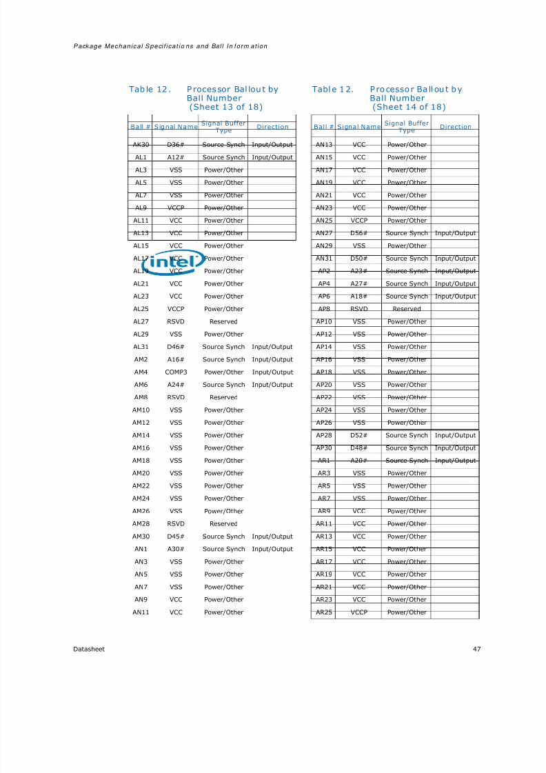
8/8/2019 Inel Dothan Proccesor
http://slidepdf.com/reader/full/inel-dothan-proccesor 47/65
Package Mechan ica l Speci f i ca t io ns and Ba l l In fo rm a t ion
Datasheet 47
AK30 D36# Source Synch Input/Output
AL1 A12# Source Synch Input/Output
AL3 VSS Power/Other
AL5 VSS Power/Other
AL7 VSS Power/Other
AL9 VCCP Power/Other
AL11 VCC Power/Other
AL13 VCC Power/Other
AL15 VCC Power/Other
AL17 VCC Power/Other
AL19 VCC Power/Other
AL21 VCC Power/Other
AL23 VCC Power/Other
AL25 VCCP Power/Other
AL27 RSVD Reserved
AL29 VSS Power/Other
AL31 D46# Source Synch Input/Output
AM2 A16# Source Synch Input/Output
AM4 COMP3 Power/Other Input/Output
AM6 A24# Source Synch Input/Output
AM8 RSVD Reserved
AM10 VSS Power/Other
AM12 VSS Power/Other
AM14 VSS Power/Other
AM16 VSS Power/Other
AM18 VSS Power/Other
AM20 VSS Power/Other
AM22 VSS Power/Other
AM24 VSS Power/Other
AM26 VSS Power/Other
AM28 RSVD Reserved
AM30 D45# Source Synch Input/Output
AN1 A30# Source Synch Input/Output
AN3 VSS Power/Other
AN5 VSS Power/Other
AN7 VSS Power/Other
AN9 VCC Power/Other
AN11 VCC Power/Other
Tab le 12 . P roces sor Bal lou t byBall Number(Sheet 13 of 18)
Ball # S ignal Name Signal BufferType Direction
AN13 VCC Power/Other
AN15 VCC Power/Other
AN17 VCC Power/Other
AN19 VCC Power/Other
AN21 VCC Power/Other
AN23 VCC Power/Other
AN25 VCCP Power/Other
AN27 D56# Source Synch Input/Output
AN29 VSS Power/Other
AN31 D50# Source Synch Input/Output
AP2 A23# Source Synch Input/Output
AP4 A27# Source Synch Input/Output
AP6 A18# Source Synch Input/Output
AP8 RSVD Reserved
AP10 VSS Power/Other
AP12 VSS Power/Other
AP14 VSS Power/Other
AP16 VSS Power/Other
AP18 VSS Power/Other
AP20 VSS Power/Other
AP22 VSS Power/Other
AP24 VSS Power/Other
AP26 VSS Power/Other
AP28 D52# Source Synch Input/Output
AP30 D48# Source Synch Input/Output
AR1 A20# Source Synch Input/Output
AR3 VSS Power/Other
AR5 VSS Power/Other
AR7 VSS Power/Other
AR9 VCC Power/Other
AR11 VCC Power/Other
AR13 VCC Power/Other
AR15 VCC Power/Other
AR17 VCC Power/Other
AR19 VCC Power/Other
AR21 VCC Power/Other
AR23 VCC Power/Other
AR25 VCCP Power/Other
Tabl e 1 2. P ro cesso r Ba ll ou t b yBall Number(Sheet 14 of 18)
Ball # Signal Name Signal BufferType Direction

8/8/2019 Inel Dothan Proccesor
http://slidepdf.com/reader/full/inel-dothan-proccesor 48/65
Package Mechan ica l Spec i f i ca t ions and Ba l l In fo rm a t ion
48 Datasheet
AR27 D55# Source Synch Input/Output
AR29 VSS Power/Other
AR31 D53# Source Synch Input/Output
AT2 ADSTB1# Source Synch Input/Output
AT4 A31# Source Synch Input/Output
AT6 A25# Source Synch Input/Output
AT8 RSVD Reserved
AT10 VSS Power/Other
AT12 VSS Power/Other
AT14 VSS Power/Other
AT16 VSS Power/OtherAT18 VSS Power/Other
AT20 VSS Power/Other
AT22 VSS Power/Other
AT24 VSS Power/Other
AT26 VSS Power/Other
AT28 D54# Source Synch Input/Output
AT30 D57# Source Synch Input/Output
AU1 A21# Source Synch Input/Output
AU3 VSS Power/Other
AU5 VSS Power/Other
AU7 VSS Power/Other
AU9 VCC Power/Other
AU11 VCC Power/Other
AU13 VCC Power/Other
AU15 VCC Power/Other
AU17 VCC Power/Other
AU19 VCC Power/Other
AU21 VCC Power/Other
AU23 VCC Power/Other
AU25 VCC Power/Other
AU27 D60# Source Synch Input/Output
AU29 VSS Power/Other
AU31 D49# Source Synch Input/Output
AV2 A26# Source Synch Input/Output
AV4 A28# Source Synch Input/Output
AV6 A19# Source Synch Input/Output
AV8 RSVD Reserved
AV10 VSS Power/Other
Tab le 12 . P ro cess or Bal lo ut byBall Number(Sheet 15 of 18)
Ball # Signal Name Signal BufferType Direction
AV12 VSS Power/Other
AV14 VSS Power/Other
AV16 VSS Power/Other
AV18 VSS Power/Other
AV20 VSS Power/Other
AV22 VSS Power/Other
AV24 VSS Power/Other
AV26 VSS Power/Other
AV28 D61# Source Synch Input/Output
AV30 D63# Source Synch Input/Output
AW1 A22# Source Synch Input/OutputAW3 VSS Power/Other
AW5 VSS Power/Other
AW7 VSS Power/Other
AW9 VCC Power/Other
AW11 VCC Power/Other
AW13 VCC Power/Other
AW15 VCC Power/Other
AW17 VCC Power/Other
AW19 VCC Power/Other
AW21 VCC Power/Other
AW23 VCC Power/Other
AW25 VCC Power/Other
AW27 D59# Source Synch Input/Output
AW29 VSS Power/Other
AW31 DSTBP3# Source Synch Input/Output
AY2 A29# Source Synch Input/Output
AY4 A17# Source Synch Input/Output
AY6 VID1 CMOS Output
AY8 PSI# CMOS Output
AY10 VSS Power/Other
AY12 VSS Power/Other
AY14 VSS Power/Other
AY16 VSS Power/Other
AY18 VSS Power/Other
AY20 VSS Power/Other
AY22 VSS Power/Other
AY24 VSS Power/Other
AY26 VSS Power/Other
Tabl e 1 2. P ro cesso r B al lo ut byBall Number(Sheet 16 of 18)
Ball # Signal Name Signal BufferType Direction

8/8/2019 Inel Dothan Proccesor
http://slidepdf.com/reader/full/inel-dothan-proccesor 49/65
Package Mechan ica l Speci f i ca t io ns and Ba l l In fo rm a t ion
Datasheet 49
AY28 D62# Source Synch Input/Output
AY30 DSTBN3# Source Synch Input/Output
BA1 VSS Power/Other
BA3 VID4 CMOS Output
BA5 VSS Power/Other
BA7 VSS Power/Other
BA9 VCC Power/Other
BA11 VCC Power/Other
BA13 VCC Power/Other
BA15 VCC Power/Other
BA17 VCC Power/Other
BA19 VCC Power/Other
BA21 VCC Power/Other
BA23 VCC Power/Other
BA25 VCC Power/Other
BA27 D51# Source Synch Input/Output
BA29 VSS Power/Other
BA31 VSS Power/Other
BB2 VSS Power/Other
BB4 VID5 CMOS Output
BB6 VID2 CMOS Output
BB8 RSVD Reserved
BB10 VSS Power/Other
BB12 VSS Power/Other
BB14 VSS Power/Other
BB16 VSS Power/Other
BB18 VSS Power/Other
BB20 VSS Power/Other
BB22 VSS Power/Other
BB24 VSS Power/Other
BB26 VSS Power/Other
BB28 DINV3# Source Synch Input/Output
BB30 VSS Power/Other
BC3 VSS Power/Other
BC5 VID3 CMOS Output
BC7 VID0 CMOS Output
BC9 VCC Power/Other
BC11 VCC Power/Other
Tab le 12 . P roces sor Bal lou t byBall Number(Sheet 17 of 18)
Ball # S ignal Name Signal BufferType Direction
BC13 VCC Power/Other
BC15 VCC Power/Other
BC17 VCC Power/Other
BC19 VCC Power/Other
BC21 VCC Power/Other
BC23 VCC Power/Other
BC25 VCC Power/Other
BC27 D58# Source Synch Input/Output
BC29 VSS Power/Other
Tabl e 1 2. P ro cesso r Ba ll ou t b yBall Number(Sheet 18 of 18)
Ball # Signal Name Signal BufferType Direction

8/8/2019 Inel Dothan Proccesor
http://slidepdf.com/reader/full/inel-dothan-proccesor 50/65
Package Mechan ica l Spec i f i ca t ions and Ba l l In fo rm a t ion
50 Datasheet
4.3 Alphabetical Signals Reference
Tab le 13. Signal Descr ip ti on (Shee t 1 o f 8 )
Name Type Description
A[31:3]# Input/Output
A[31:3]# (Address) define a 2 32 -byte physical memory addressspace. In sub-phase 1 of the address phase, these pins transmitthe address of a transaction. In sub-phase 2, these pins transmittransaction type information. These signals must connect theappropriate pins of both agents on the Intel ® Processor FSB.A[31:3]# are source synchronous signals and are latched into thereceiving buffers by ADSTB[1:0]#. Address signals are used asstraps which are sampled before RESET# is de-asserted.
A20M# Input
If A20M# (Address-20 Mask) is asserted, the processor masksphysical address bit 20 (A20#) before looking up a line in anyinternal cache and before driving a read/write transaction on thebus. Asserting A20M# emulates the 8086 processor's addresswrap-around at the 1-Mbyte boundary. Assertion of A20M# is onlysupported in real mode.A20M# is an asynchronous signal. However, to ensure recognitionof this signal following an Input/Output write instruction, it mustbe valid along with the TRDY# assertion of the correspondingInput/Output Write bus transaction.
ADS# Input/Output
ADS# (Address Strobe) is asserted to indicate the validity of thetransaction address on the A[31:3]# and REQ[4:0]# pins. All busagents observe the ADS# activation to begin parity checking,protocol checking, address decode, internal snoop, or deferredreply ID match operations associated with the new transaction.
ADSTB[1:0]# Input/Output
Address strobes are used to latch A[31:3]# and REQ[4:0]# ontheir rising and falling edges. Strobes are associated with signalsas shown below.
BCLK[1:0] Input
The differential pair BCLK (Bus Clock) determines the FSBfrequency. All FSB agents must receive these signals to drive theiroutputs and latch their inputs.All external timing parameters are specified with respect to therising edge of BCLK0 crossing V CROSS .
BNR# Input/Output
BNR# (Block Next Request) is used to assert a bus stall by anybus agent who is unable to accept new bus transactions. During abus stall, the current bus owner cannot issue any newtransactions.
BPM[2:0]#BPM3
OutputInput/Output
BPM[3:0]# (Breakpoint Monitor) are breakpoint and performancemonitor signals. They are outputs from the processor whichindicate the status of breakpoints and programmable countersused for monitoring processor performance. BPM[3:0]# shouldconnect the appropriate pins of all Intel ® processor FSBagents.This includes debug or performance monitoring tools.
Signals Associated Strobe
REQ[4:0]#, A[16:3]# ADSTB[0]#
A[31:17]# ADSTB[1]#

8/8/2019 Inel Dothan Proccesor
http://slidepdf.com/reader/full/inel-dothan-proccesor 51/65
Datasheet 51
Package Mechan ica l Speci f i ca t io ns and Ba l l In fo rm a t ion
BPRI# Input
BPRI# (Bus Priority Request) is used to arbitrate for ownership of the FSB. It must connect the appropriate pins of both FSB agents.Observing BPRI# active (as asserted by the priority agent) causesthe other agent to stop issuing new requests, unless suchrequests are part of an ongoing locked operation. The priorityagent keeps BPRI# asserted until all of its requests arecompleted, then releases the bus by de-asserting BPRI#.
BR0# Input/Output
BR0# is used by the processor to request the bus. The arbitrationis done between Intel processor (Symmetric Agent) and Intel945GU chipset family GMCH (High Priority Agent).
BSEL[1:0] Output
These signals are used to select the FSB clock frequency. Theyshould be connected between the processor and the chipsetGMCH and clock generator on Intel 945GU chipset family basedplatforms.
COMP[3:0] Analog COMP[3:0] must be terminated on the system board using
precision (1% tolerance) resistors.
D[63:0]# Input/Output
D[63:0]# (Data) are the data signals. These signals provide a 64-bit data path between the FSB agents, and must connect theappropriate pins on both agents. The data driver asserts DRDY#to indicate a valid data transfer.D[63:0]# are quad-pumped signals and will thus be driven fourtimes in a common clock period. D[63:0]# are latched off thefalling edge of both DSTBP[3:0]# and DSTBN[3:0]#. Each groupof 16 data signals correspond to a pair of one DSTBP# and oneDSTBN#. The following table shows the grouping of data signalsto data strobes and DINV# .
Furthermore, the DINV# pins determine the polarity of the datasignals. Each group of 16 data signals corresponds to one DINV#signal. When the DINV# signal is active, the corresponding datagroup is inverted and therefore sampled active high.
DBR# Output
DBR# (Data Bus Reset) is used only in processor systems whereno debug port is implemented on the system board. DBR# is usedby a debug port interposer so that an in-target probe can drivesystem reset. If a debug port is implemented in the system,DBR# is a no connect in the system. DBR# is not a processorsignal.
DBSY# Input/Output
DBSY# (Data Bus Busy) is asserted by the agent responsible fordriving data on the FSB to indicate that the data bus is in use. Thedata bus is released after DBSY# is de-asserted. This signal mustconnect the appropriate pins on both FSB agents.
Tab le 13. Signal Descr ip ti on (Shee t 2 o f 8 )
Name Type Description
Quad-Pumped Signal Groups
Data Group DSTBN#/
DSTBP#DINV#
D[15:0]# 0 0
D[31:16]# 1 1
D[47:32]# 2 2
D[63:48]# 3 3

8/8/2019 Inel Dothan Proccesor
http://slidepdf.com/reader/full/inel-dothan-proccesor 52/65

8/8/2019 Inel Dothan Proccesor
http://slidepdf.com/reader/full/inel-dothan-proccesor 53/65
Datasheet 53
Package Mechan ica l Speci f i ca t io ns and Ba l l In fo rm a t ion
DSTBP[3:0]# Input/Output
Data strobe used to latch in D[63:0]#.
FERR#/PBE# Output
FERR# (Floating-point Error)PBE#(Pending Break Event) is amultiplexed signal and its meaning is qualified with STPCLK#.When STPCLK# is not asserted, FERR#/PBE# indicates a floatingpoint when the processor detects an unmasked floating-pointerror. FERR# is similar to the ERROR# signal on the Intel 387coprocessor, and is included for compatibility with systems using
MS-DOS*-type floating-point error reporting. When STPCLK# isasserted, an assertion of FERR#/PBE# indicates that theprocessor has a pending break event waiting for service. Theassertion of FERR#/PBE# indicates that the processor should bereturned to the Normal state. When FERR#/PBE# is asserted,indicating a break event, it will remain asserted until STPCLK# isde-asserted. Assertion of PREQ# when STPCLK# is active will alsocause an FERR# break event.For additional information on the pending break eventfunctionality, including identification of support of the feature andenable/disable information, refer to Volume 3 of the Intel ®
Architecture Software Developer’s Manual and the Intel ®
Processor Identification and CPUID Instruction Application Note .
GTLREF InputGTLREF determines the signal reference level for AGTL+ inputpins. GTLREF should be set at 2/3 V CCP. GTLREF is used by theAGTL+ receivers to determine if a signal is a logical 0 or logical 1.
HIT#
HITM#
Input/Output
Input/Output
HIT# (Snoop Hit) and HITM# (Hit Modified) convey transactionsnoop operation results. Either FSB agent may assert both HIT#and HITM# together to indicate that it requires a snoop stall,which can be continued by reasserting HIT# and HITM# together.
IERR# Output
IERR# (Internal Error) is asserted by a processor as the result of an internal error. Assertion of IERR# is usually accompanied by aSHUTDOWN transaction on the FSB. This transaction mayoptionally be converted to an external error signal (e.g., NMI) bysystem core logic. The processor will keep IERR# asserted untilthe assertion of RESET#, BINIT#, or INIT#.
Tab le 13. Signal Descr ip ti on (Shee t 4 o f 8 )
Name Type Description
Signals Associated Strobe
D[15:0]#, DINV0# DSTBP0#
D[31:16]#, DINV1# DSTBP1#
D[47:32]#, DINV2# DSTBP2#
D[63:48]#, DINV3# DSTBP3#

8/8/2019 Inel Dothan Proccesor
http://slidepdf.com/reader/full/inel-dothan-proccesor 54/65
Package Mechan ica l Spec i f i ca t ions and Ba l l In fo rm a t ion
54 Datasheet
IGNNE# Input
IGNNE# (Ignore Numeric Error) is asserted to force the processorto ignore a numeric error and continue to execute noncontrolfloating-point instructions. If IGNNE# is de-asserted, theprocessor generates an exception on a noncontrol floating-pointinstruction if a previous floating-point instruction caused an error.IGNNE# has no effect when the NE bit in control register 0 (CR0)is set.IGNNE# is an asynchronous signal. However, to ensurerecognition of this signal following an Input/Output writeinstruction, it must be valid along with the TRDY# assertion of thecorresponding Input/Output Write bus transaction.
INIT# Input
INIT# (Initialization), when asserted, resets integer registersinside the processor without affecting its internal caches orfloating-point registers. The processor then begins execution atthe power-on Reset vector configured during power-onconfiguration. The processor continues to handle snoop requests
during INIT# assertion. INIT# is an asynchronous signal.However, to ensure recognition of this signal following an Input/Output Write instruction, it must be valid along with the TRDY#assertion of the corresponding Input/Output Write bustransaction. INIT# must connect the appropriate pins of both FSBagents.If INIT# is sampled active on the active to inactive transition of RESET#, then the processor executes its Built-in Self-Test (BIST).
ITP_CLK[1:0] Input
ITP_CLK[1:0] are copies of BCLK that are used only in processorsystems where no debug port is implemented on the systemboard. ITP_CLK[1:0] are used as BCLK[1:0] references for adebug port implemented on an interposer. If a debug port isimplemented in the system, ITP_CLK[1:0] are no connects in thesystem. These are not processor signals.
LINT[1:0] Input
LINT[1:0] (Local APIC Interrupt) must connect the appropriatepins of all APIC Bus agents. When the APIC is disabled, the LINT0signal becomes INTR, a maskable interrupt request signal, andLINT1 becomes NMI, a nonmaskable interrupt. INTR and NMI arebackward compatible with the signals of those names on thePentium processor. Both signals are asynchronous.Both of these signals must be software configured via BIOSprogramming of the APIC register space to be used either as NMI/INTR or LINT[1:0]. Because the APIC is enabled by default afterreset, operation of these pins as LINT[1:0] is the defaultconfiguration.
LOCK# Input/Output
LOCK# indicates to the system that a transaction must occuratomically. This signal must connect the appropriate pins of bothFSB agents. For a locked sequence of transactions, LOCK# isasserted from the beginning of the first transaction to the end of the last transaction.When the priority agent asserts BPRI# to arbitrate for ownershipof the FSB, it will wait until it observes LOCK# de-asserted. Thisenables symmetric agents to retain ownership of the FSBthroughout the bus locked operation and ensure the atomicity of lock.
PRDY# Output Probe Ready signal used by debug tools to determine processordebug readiness.
Tab le 13. Signal Descr ip ti on (Shee t 5 o f 8 )
Name Type Description

8/8/2019 Inel Dothan Proccesor
http://slidepdf.com/reader/full/inel-dothan-proccesor 55/65
Datasheet 55
Package Mechan ica l Speci f i ca t io ns and Ba l l In fo rm a t ion
PREQ# Input Probe Request signal used by debug tools to request debugoperation of the processor.
PROCHOT# Output
PROCHOT# (Processor Hot) will go active when the processortemperature monitoring sensor detects that the processor hasreached its maximum safe operating temperature. This indicatesthat the processor Thermal Control Circuit has been activated, if enabled. See Chapter 5 for more details.This signal may require voltage translation on the motherboard.
PSI# OutputProcessor Power Status Indicator signal. This signal is assertedwhen the processor is in a lower state (Deep Sleep and DeeperSleep). See Section 2.1.6 for more details.
PWRGOOD Input
PWRGOOD (Power Good) is a processor input. The processorrequires this signal to be a clean indication that the clocks andpower supplies are stable and within their specifications. Cleanimplies that the signal will remain low (capable of sinking leakage
current), without glitches, from the time that the power suppliesare turned on until they come within specification. The signalmust then transition monotonically to a high state.The PWRGOOD signal must be supplied to the processor; it isused to protect internal circuits against voltage sequencingissues. It should be driven high throughout boundary scanoperation.
REQ[4:0]# Input/Output
REQ[4:0]# (Request Command) must connect the appropriatepins of both FSB agents. They are asserted by the current busowner to define the currently active transaction type. Thesesignals are source synchronous to ADSTB0#.
RESET# Input
Asserting the RESET# signal resets the processor to a knownstate and invalidates its internal caches without writing back anyof their contents. For a power-on Reset, RESET# must stay active
for at least two milliseconds after V CC and BCLK have reachedtheir proper specifications. On observing active RESET#, both FSBagents will de-assert their outputs within two clocks. All processorstraps must be valid within the specified setup time beforeRESET# is de-asserted.There is a 55 ohm (nominal) on die pull-up resistor on this signal.
RS[2:0]# InputRS[2:0]# (Response Status) are driven by the response agent(the agent responsible for completion of the current transaction),and must connect the appropriate pins of both FSB agents.
RSVDReserved/
NoConnect
These pins are RESERVED and must be left unconnected on theboard. However, it is recommended that routing channels to thesepins on the board be kept open for possible future use.
Tab le 13. Signal Descr ip ti on (Shee t 6 o f 8 )
Name Type Description

8/8/2019 Inel Dothan Proccesor
http://slidepdf.com/reader/full/inel-dothan-proccesor 56/65
Package Mechan ica l Spec i f i ca t ions and Ba l l In fo rm a t ion
56 Datasheet
SLP# Input
SLP# (Sleep), when asserted in Stop-Grant state, causes theprocessor to enter the Sleep state. During Sleep state, theprocessor stops providing internal clock signals to all units,leaving only the Phase-Locked Loop (PLL) still operating.Processors in this state will not recognize snoops or interrupts.The processor will recognize only assertion of the RESET# signal,de-assertion of SLP#, and removal of the BCLK input while inSleep state. If SLP# is de-asserted, the processor exits Sleepstate and returns to Stop-Grant state, restarting its internal clocksignals to the bus and processor core units. If DPSLP# is assertedwhile in the Sleep state, the processor will exit the Sleep stateand transition to the Deep Sleep state.
SMI# Input
SMI# (System Management Interrupt) is asserted asynchronouslyby system logic. On accepting a System Management Interrupt,the processor saves the current state and enter SystemManagement mode (SMM). An SMI Acknowledge transaction is
issued, and the processor begins program execution from theSMM handler.If SMI# is asserted during the de-assertion of RESET# theprocessor will tristate its outputs.
STPCLK# Input
STPCLK# (Stop Clock), when asserted, causes the processor toenter a low power Stop-Grant state. The processor issues a Stop-Grant Acknowledge transaction, and stops providing internal clocksignals to all processor core units except the FSB and APIC units.The processor continues to snoop bus transactions and serviceinterrupts while in Stop-Grant state. When STPCLK# is de-asserted, the processor restarts its internal clock to all units andresumes execution. The assertion of STPCLK# has no effect onthe bus clock; STPCLK# is an asynchronous input.
TCK Input TCK (Test Clock) provides the clock input for the processor testbus (also known as the Test Access Port).
TDI InputTDI (Test Data In) transfers serial test data into the processor.TDI provides the serial input needed for JTAG specificationsupport.
TDO OutputTDO (Test Data Out) transfers serial test data out of theprocessor. TDO provides the serial output needed for JTAGspecification support.
TEST1, TEST2 Input TEST1 and TEST2 must have a stuffing option of separate pulldown resistors to V SS .
THERMDA Other Thermal Diode Anode.
THERMDC Other Thermal Diode Cathode.
THERMTRIP# Output
The processor protects itself from catastrophic overheating by useof an internal thermal sensor. This sensor is set well above thenormal operating temperature to ensure that there are no falsetrips. The processor will stop all execution when the junctiontemperature exceeds approximately 125°C. This is signalled tothe system by the THERMTRIP# (Thermal Trip) pin.
TMS Input TMS (Test Mode Select) is a JTAG specification support signal usedby debug tools.
Tab le 13. Signal Descr ip ti on (Shee t 7 o f 8 )
Name Type Description

8/8/2019 Inel Dothan Proccesor
http://slidepdf.com/reader/full/inel-dothan-proccesor 57/65
Datasheet 57
Package Mechan ica l Speci f i ca t io ns and Ba l l In fo rm a t ion
§ §
TRDY# InputTRDY# (Target Ready) is asserted by the target to indicate that itis ready to receive a write or implicit writeback data transfer.TRDY# must connect the appropriate pins of both FSB agents.
TRST# Input TRST# (Test Reset) resets the Test Access Port (TAP) logic. TRST#must be driven low during power on Reset.
VCC Input Processor core power supply.
VCCA Input VCCA provides isolated power for the internal processor corePLLs.
VCCP Input Processor I/O power supply.
VCCQ[1:0] Input
Quiet power supply for on die COMP circuitry. These pins shouldbe connected to V CCP on the motherboard. However, theseconnections should enable addition of decoupling on the VCCQ lines if necessary.
VCCSENSE OutputVCCSENSE is an isolated low impedance connection to processorcore power (V CC). It can be used to sense or measure power nearthe silicon with little noise.
VID[5:0] Output
VID[5:0] (Voltage ID) pins are used to support automaticselection of power supply voltages (V CC). Unlike some previousgenerations of processors, these are CMOS signals that are drivenby the processor. The voltage supply for these pins must be validbefore the VR can supply V CC to the processor. Conversely, the VRoutput must be disabled until the voltage supply for the VID pinsbecomes valid. The VID pins are needed to support the processorvoltage specification variations. See Table 2 for definitions of these pins. The VR must supply the voltage that is requested bythe pins, or disable i tself.
VSSSENSE OutputVSSSENSE is an isolated low impedance connection to processorcore V SS . It can be used to sense or measure ground near the
silicon with little noise.
Tab le 13. Signal Descr ip ti on (Shee t 8 o f 8 )
Name Type Description

8/8/2019 Inel Dothan Proccesor
http://slidepdf.com/reader/full/inel-dothan-proccesor 58/65
Package Mechan ica l Spec i f i ca t ions and Ba l l In fo rm a t ion
58 Datasheet

8/8/2019 Inel Dothan Proccesor
http://slidepdf.com/reader/full/inel-dothan-proccesor 59/65
Datasheet 59
Therma l Spec i f i ca t ions and Des ign Cons ide ra t ions
5 Th er m al Sp eci f i ca t i o n s an d D e si g n Co n s i d e r a t i o n s
The processor requires a thermal solution to maintain temperatures within operatinglimits as set forth in Section 5.1 . Any attempt to operate that processor outside theseoperating limits may result in permanent damage to the processor and potentially othercomponents in the system. As processor technology changes, thermal managementbecomes increasingly crucial when building computer systems. Maintaining the properthermal environment is key to reliable, long-term system operation. A completethermal solution includes both component and system level thermal managementfeatures. Component level thermal solutions include active or passive heatsinks or heatexchangers attached to the processor exposed die. The solution should make firmcontact to the die while maintaining processor mechanical specifications, such aspressure. A typical system level thermal solution may consist of a processor fan ductedto a heat exchanger that is thermally coupled to the processor via a heat pipe or directdie attachment. A secondary fan or air from the processor fan may also be used to cool
other platform components or lower the internal ambient temperature within thesystem.
To allow for the optimal operation and long-term reliability of Intel processor-basedsystems, the system/processor thermal solution should be designed such that theprocessor must remain within the minimum and maximum junction temperature (Tj)specifications at the corresponding thermal design power (TDP) value listed in Table 14 and Table 15 . Thermal solutions not design to provide this level of thermal capabilitymay affect the long-term reliability of the processor and system.
The maximum junction temperature is defined by an activation of the processor IntelThermal Monitor. Refer to Section 5.1.3 for more details. Analysis indicates that realapplications are unlikely to cause the processor to consume the theoretical maximumpower dissipation for sustained time periods. Intel recommends that complete thermalsolution designs target the TDP indicated in Table 14 and Table 15 . The Intel ThermalMonitor feature is designed to help protect the processor in the unlikely event that anapplication exceeds the TDP recommendation for a sustained period of time. For moredetails on the usage of this feature, refer to Section 5.1.3 . In all cases the IntelThermal Monitor feature must be enabled for the processor to remain withinspecification.

8/8/2019 Inel Dothan Proccesor
http://slidepdf.com/reader/full/inel-dothan-proccesor 60/65
Therma l Spec i f i ca t ions and Des ign Cons ide ra t ions
60 Datasheet
NOTES:1. The TDP specification should be used to design the processor thermal solution. The TDP is
not the maximum theoretical power the processor can generate.2. Not 100% tested. These power specifications are determined by characterization of the
processor currents at higher temperatures and extrapolating the values for thetemperature indicated.
Table 14 . Processor Power Speci fica t ions (3 W processors)
Symbol Core F requency and Vol tage The rmal Des ign Power Uni t No tes
HFM TDP 800 MHz and HFM V CC 3 W At 100°C,Notes 1
LFM TDP 600 MHz and LFM V CC 3 W At 100°C,Notes 1
Symbol Parameter Min Typ Max Unit Notes
PAH, P SGNT Auto Halt, Stop Grant PowerLFMHFM
— — 1.01.1
W At 50°C,Notes 2
PSLP Sleep PowerLFMHFM
— — 0.80.9
W At 50°C,Notes 2
PDSLP Deep Sleep PowerLFMHFM
— — 0.650.7
W At 35°C,
Notes 2
PDPRSLP Deeper Sleep Power at (C4) 0.7 V — — 0.4 W At 35°C,Notes 2
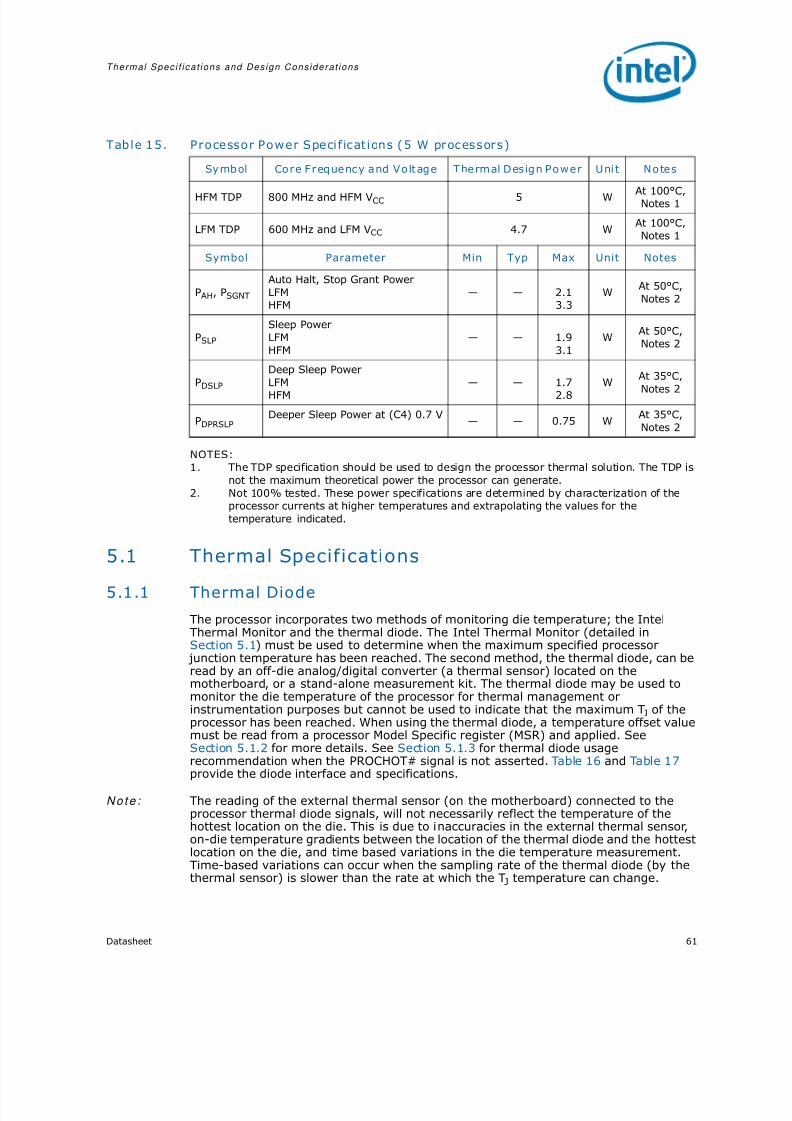
8/8/2019 Inel Dothan Proccesor
http://slidepdf.com/reader/full/inel-dothan-proccesor 61/65
Datasheet 61
Therma l Spec i f i ca t ions and Des ign Cons ide ra t ions
NOTES:1. The TDP specification should be used to design the processor thermal solution. The TDP is
not the maximum theoretical power the processor can generate.2. Not 100% tested. These power specifications are determined by characterization of the
processor currents at higher temperatures and extrapolating the values for thetemperature indicated.
5.1 Thermal Specifications
5.1.1 Thermal DiodeThe processor incorporates two methods of monitoring die temperature; the IntelThermal Monitor and the thermal diode. The Intel Thermal Monitor (detailed inSection 5.1 ) must be used to determine when the maximum specified processor
junction temperature has been reached. The second method, the thermal diode, can beread by an off-die analog/digital converter (a thermal sensor) located on themotherboard, or a stand-alone measurement kit. The thermal diode may be used tomonitor the die temperature of the processor for thermal management orinstrumentation purposes but cannot be used to indicate that the maximum T J of theprocessor has been reached. When using the thermal diode, a temperature offset valuemust be read from a processor Model Specific register (MSR) and applied. SeeSection 5.1.2 for more details. See Section 5.1.3 for thermal diode usagerecommendation when the PROCHOT# signal is not asserted. Table 16 and Table 17 provide the diode interface and specifications.
N o t e : The reading of the external thermal sensor (on the motherboard) connected to theprocessor thermal diode signals, will not necessarily reflect the temperature of thehottest location on the die. This is due to inaccuracies in the external thermal sensor,on-die temperature gradients between the location of the thermal diode and the hottestlocation on the die, and time based variations in the die temperature measurement.Time-based variations can occur when the sampling rate of the thermal diode (by thethermal sensor) is slower than the rate at which the T J temperature can change.
Table 15 . Processor Power Speci f icat ions (5 W processors)
Symbol Core F requency and Vo lt age The rmal Des ign Power Uni t No tes
HFM TDP 800 MHz and HFM V CC 5 W At 100°C,Notes 1
LFM TDP 600 MHz and LFM V CC 4.7 W At 100°C,Notes 1
Symbol Parameter Min Typ Max Unit Notes
PAH, P SGNT Auto Halt, Stop Grant PowerLFMHFM
— — 2.13.3
W At 50°C,Notes 2
PSLP Sleep PowerLFMHFM
— — 1.93.1
W At 50°C,Notes 2
PDSLP Deep Sleep PowerLFMHFM
— — 1.72.8
W At 35°C,
Notes 2
PDPRSLP Deeper Sleep Power at (C4) 0.7 V — — 0.75 W At 35°C,Notes 2

8/8/2019 Inel Dothan Proccesor
http://slidepdf.com/reader/full/inel-dothan-proccesor 62/65
Therma l Spec i f i ca t ions and Des ign Cons ide ra t ions
62 Datasheet
Offset between the thermal diode based temperature reading and the Intel ThermalMonitor reading may be characterized using the Intel Thermal Monitor’s Automaticmode activation of thermal control circuit. This temperature offset must be taken intoaccount when using the processor thermal diode to implement power managementevents.
5.1.2 Thermal Diode Offset
A temperature offset value (specified as Toffset in Table 17 ) will be programmed into aprocessor Model Specific Register (MSR). This offset is determined by using a thermaldiode ideality factor mean value of n = 1.0022 (shown in Table 17 ) as a reference. Thisoffset must be applied to the junction temperature read by the thermal diode. Anytemperature adjustments due to differences between the reference ideality value of 1.0022 and the default ideality values programmed into the on-board thermal sensors,will have to be made before the above offset is applied.
The thermal diode offset model specific register, THERM_DIODE_OFFSET, is located atoffset 03Fh accessed as a QWord. Bits 7:0 contain the thermal diode offset value in0.5°C resolution. This value should be subtracted from the diode measurement afterthe thermal diode ideality adjustments are made. Values from bits 7:0 of the MSR areinterpreted as follows:
• ‘00000000’ = 0°C
• ‘00000001’ = +0.5°C
• ‘00000010’ = +1°C
• ‘01111111’ = +63.5°C
• ‘11111111’ = -0.5°C
• ‘11111110’ = -1°C
• ‘1000000’ = -64°C
Tab le 1 6. T he rm al D io de I n te rf ac e
Signal Name Pin/ Ball Number Signal Description
THERMDA B18 Thermal diode anode
THERMDC A18 Thermal diode cathode

8/8/2019 Inel Dothan Proccesor
http://slidepdf.com/reader/full/inel-dothan-proccesor 63/65
Datasheet 63
Therma l Spec i f i ca t ions and Des ign Cons ide ra t ions
NOTES:1. Intel does not support or recommend operation of the thermal diode under reverse bias.
Intel does not support or recommend operation of the thermal diode when the processorpower supplies are not within their specified tolerance range.
2. Characterized at 100°C.3. Not 100% tested. Specified by design/characterization.4. The ideality factor, n, represents the deviation from ideal diode behavior as exemplified by
the diode equation:
IFW=I s *(e (qV D /nkT) -1)
Where I S = saturation current, q = electronic charge, V D = voltage across the diode,k = Boltzmann Constant, and T = absolute temperature (Kelvin).Value shown in the table is not the processor thermal diode ideality factor. It is a referencevalue used to calculate the processor thermal diode temperature offset.
5. The series resistance, R T is provided to allow for a more accurate measurement of thediode junction temperature. R T as defined includes the pins of the processor but does notinclude any socket resistance or board trace resistance between the socket and theexternal remote diode thermal sensor. R T can be used by remote diode thermal sensorswith automatic series resistance cancellation to calibrate out this error term. Anotherapplication is that a temperature offset can be manually calculated and programmed intoan offset register in the remote diode thermal sensors as exemplified by the equation:
Terror = [R T*(N-1)*I FWmin ]/[(no/q)*ln N
6. Offset value is programmed in processor Model Specific Register 03Fh, “THERM_DIODE_OFFSET”.
5.1.3 I ntel ® Thermal Monitor
The Intel Thermal Monitor helps control the processor temperature by activating theTCC when the processor silicon reaches its maximum operating temperature. Thetemperature at which Intel Thermal Monitor activates the thermal control circuit is notuser configurable and is not software visible. Bus traffic is snooped in the normalmanner, and interrupt requests are latched (and serviced during the time that theclocks are on) while the TCC is active.
With a properly designed and characterized thermal solution, it is anticipated that the
TCC would only be activated for very short periods of time when running the mostpower intensive applications. The processor performance impact due to these brief periods of TCC activation is expected to be so minor that it would not be detectable. Anunder-designed thermal solution that is not able to prevent excessive activation of theTCC in the anticipated ambient environment may cause a noticeable performance loss,and may affect the long-term reliability of the processor. In addition, a thermal solutionthat is significantly under designed may not be capable of cooling the processor evenwhen the TCC is active continuously.
Tab le 17. The rmal D iode Spec if icat ion
Symbol P arameter Min Typ Max Unit Notes
IFW Forward Bias Current 5 — 300 μA
Note 1Toffset Thermal diode temperature offset -4 — 11 °C 2, 6
n Reference Diode Ideality Factorused to calculate temperature offset
— 1.0022 — — Notes 2,3, 4
RT Series Resistance — 3.06 — Ohms 2, 3, 5

8/8/2019 Inel Dothan Proccesor
http://slidepdf.com/reader/full/inel-dothan-proccesor 64/65
Therma l Spec i f i ca t ions and Des ign Cons ide ra t ions
64 Datasheet
The Intel Thermal Monitor controls the processor temperature by modulating (startingand stopping) the processor core clocks or by initiating an Enhanced Intel SpeedSteptechnology transition when the processor silicon reaches its maximum operatingtemperature. The Intel Thermal Monitor uses two modes to activate the TCC:Automatic mode and On-Demand mode. If both modes are activated, Automatic mode
takes precedence.
Cau t ion : The Intel Thermal Monitor Automatic Mode mst be enabled via BIOS for the processorto be operating within specifications.
There are two automatic modes called Intel Thermal Monitor 1 and Intel ThermalMonitor 2. These modes are selected by writing values to the Model Specific registers(MSRs) of the processor. After Automatic mode is enabled, the TCC will activate onlywhen the internal die temperature reaches the maximum allowed value for operation.
Likewise, when Intel Thermal Monitor 2 is enabled, and a high temperature situationexists, the processor will perform an Enhanced Intel SpeedStep technology transition toa lower operating point. When the processor temperature drops below the critical level,the processor will make an Enhanced Intel SpeedStep technology transition to the lastrequested operating point. Intel Thermal Monitor 2 is the recommended mode on theprocessor.
If a processor load based Enhanced Intel SpeedStep technology transition (throughMSR write) is initiated when an Intel Thermal Monitor 2 period is active, there are twopossible results:
1. If the processor load based Enhanced Intel SpeedStep technology transition targetfrequency is higher than the Intel Thermal Monitor 2 transition based targetfrequency, the processor load-based transition will be deferred until the IntelThermal Monitor 2 event has been completed.
2. If the processor load-based Enhanced Intel SpeedStep technology transition targetfrequency is lower than the Intel Thermal Monitor 2 transition based targetfrequency, the processor will transition to the processor load-based Enhanced IntelSpeedStep technology target frequency point.
When Intel Thermal Monitor 1 is enabled, and a high temperature situation exists, the
clocks will be modulated by alternately turning the clocks off and on at a 50% dutycycle. Cycle times are processor speed dependent and will decrease linearly asprocessor core frequencies increase. Once the temperature has returned to a non-critical level, modulation ceases and TCC goes inactive. A small amount of hysteresishas been included to prevent rapid active/inactive transitions of the TCC when theprocessor temperature is near the trip point. The duty cycle is factory configured andcannot be modified. Also, automatic mode does not require any additional hardware,software drivers, or interrupt handling routines. Processor performance will bedecreased by the same amount as the duty cycle when the TCC is active; however, witha properly designed and characterized thermal solution the TCC most likely will neverbe activated, or only will be activated briefly during the most power intensiveapplications.
The TCC may also be activated via On-Demand mode. If bit 4 of the ACPI Intel ThermalMonitor Control Register is written to a 1, the TCC will be activated immediately,
independent of the processor temperature. When using On-Demand mode to activatethe TCC, the duty cycle of the clock modulation is programmable via bits 3:1 of thesame ACPI Intel Thermal Monitor Control Register. In automatic mode, the duty cycle isfixed at 50% on, 50% off, however in On-Demand mode, the duty cycle can beprogrammed from 12.5% on/ 87.5% off, to 87.5% on/12.5% off in 12.5% increments.On-Demand mode may be used at the same time Automatic mode is enabled, however,if the system tries to enable the TCC via On-Demand mode at the same time automaticmode is enabled an d a high temperature condition exists, automatic mode will takeprecedence.

8/8/2019 Inel Dothan Proccesor
http://slidepdf.com/reader/full/inel-dothan-proccesor 65/65
Therma l Spec i f i ca t ions and Des ign Cons ide ra t ions
An external signal, PROCHOT# (processor hot) is asserted when the processor detectsthat its temperature is above the thermal trip point. Bus snooping and interruptlatching are also active while the TCC is active.
Besides the thermal sensor and thermal control circuit, the Intel Thermal Monitor
feature also includes one ACPI register, one performance counter register, three modelspecific registers (MSR), and one I/O pin (PROCHOT#). All are available to monitor andcontrol the state of the Intel Thermal Monitor feature. The Intel Thermal Monitor can beconfigured to generate an interrupt upon the assertion or de-assertion of PROCHOT#.
N o t e : PROCHOT# will not be asserted when the processor is in the Stop Grant, Sleep, DeepSleep, and Deeper Sleep low power states (internal clocks stopped), hence the thermaldiode reading must be used as a safeguard to maintain the processor junctiontemperature within the 100°C (maximum) specification. If the platform thermalsolution is not able to maintain the processor junction temperature within themaximum specification, the system must initiate an orderly shutdown to preventdamage. If the processor enters one of the above low power states with PROCHOT#already asserted, PROCHOT# will remain asserted until the processor exits the LowPower state and the processor junction temperature drops below the thermal trip point.
If automatic mode is disabled, the processor will be operating out of specification.Regardless of enabling the automatic or On-Demand modes, in the event of acatastrophic cooling failure, the processor will automatically shut down when the siliconhas reached a temperature of approximately 125°C. At this point the FSB signalTHERMTRIP# will go active. THERMTRIP# activation is independent of processoractivity and does not generate any bus cycles. When THERMTRIP# is asserted, theprocessor core voltage must be shut down within the time specified in Chapter 3 .
§ §


