
Intel® Stratix® 10 Avalon-STInterface for PCIe Solutions UserGuideUG-200322017.05.08
Last updated for Intel® Quartus® Prime Design Suite: Quartus Prime Pro v17.1 Stratix 10 Editions
SubscribeSend Feedback

Contents
1 Introduction.................................................................................................................... 61.1 Avalon-ST Interface for PCIe Introduction.................................................................. 61.2 Features................................................................................................................71.3 Release Information ...............................................................................................81.4 Device Family Support ............................................................................................81.5 Recommended Speed Grades................................................................................... 91.6 Performance and Resource Utilization ....................................................................... 91.7 Transceiver Tiles................................................................................................... 101.8 PCI Express IP Core Package Layout........................................................................111.9 Channel Availability...............................................................................................15
2 Quick Start Guide...........................................................................................................172.1 Design Components.............................................................................................. 182.2 Directory Structure............................................................................................... 192.3 Generating the Design...........................................................................................202.4 Simulating the Design........................................................................................... 212.5 Compiling the Design............................................................................................ 23
3 Interface Overview........................................................................................................ 25
4 Parameters ................................................................................................................... 314.1 Stratix 10 Avalon-ST Settings................................................................................. 314.2 Base Address Registers..........................................................................................324.3 Device Identification Registers................................................................................324.4 PCI Express and PCI Capabilities Parameters............................................................ 33
4.4.1 Device Capabilities.................................................................................... 334.4.2 Link Capabilities .......................................................................................334.4.3 MSI and MSI-X Capabilities ....................................................................... 344.4.4 Slot Capabilities .......................................................................................344.4.5 Power Management ..................................................................................354.4.6 Vendor Specific Extended Capability (VSEC)................................................. 36
4.5 Configuration, Debug and Extension Options............................................................ 364.6 PHY Characteristics .............................................................................................. 364.7 Stratix 10 Example Designs....................................................................................37
5 Designing with the IP Core............................................................................................ 385.1 Generation...........................................................................................................385.2 Simulation........................................................................................................... 39
5.2.1 Selecting Serial or PIPE Simulation .............................................................405.2.2 Reducing Counter Values for Simulation....................................................... 40
5.3 Files Generated for Intel FPGA IP Cores and Qsys Pro Systems....................................405.4 Integration and Implementation..............................................................................43
5.4.1 Clock Requirements...................................................................................435.4.2 Reset Requirements.................................................................................. 44
5.5 Required Supporting IP Cores.................................................................................445.5.1 Hard Reset Controller................................................................................ 455.5.2 TX PLL.....................................................................................................45
5.6 Channel Layout and PLL Usage............................................................................... 45
Contents
Intel® Stratix® 10 Avalon-ST Interface for PCIe Solutions User Guide2

5.7 Compiling the Full Design and Programming the FPGA............................................... 50
6 Block Descriptions......................................................................................................... 516.1 Interfaces............................................................................................................52
6.1.1 TLP Header and Data Alignment for the Avalon-ST RX and TX Interfaces.......... 536.1.2 Avalon-ST RX Interface..............................................................................546.1.3 Avalon-ST TX Interface.............................................................................. 576.1.4 TX Credit Interface....................................................................................606.1.5 Interpreting the TX Credit Interface.............................................................616.1.6 Clocks..................................................................................................... 636.1.7 Update Flow Control Timer and Credit Release.............................................. 636.1.8 Resets.....................................................................................................636.1.9 Interrupts................................................................................................ 656.1.10 Transaction Layer Configuration Space Interface..........................................666.1.11 Configuration Extension Bus Interface........................................................686.1.12 Hard IP Status Interface...........................................................................686.1.13 Serial Data Interface............................................................................... 706.1.14 PIPE Interface.........................................................................................706.1.15 Hard IP Reconfiguration........................................................................... 736.1.16 Power Management Interface....................................................................746.1.17 Test Interface......................................................................................... 746.1.18 Message Handling................................................................................... 76
6.2 Errors reported by the Application Layer.................................................................. 776.2.1 Error Handling..........................................................................................78
6.3 Power Management...............................................................................................796.3.1 Endpoint D3 Entry ....................................................................................796.3.2 End Point D3 Exit...................................................................................... 806.3.3 Exit from D3 hot ...................................................................................... 806.3.4 Exit from D3 cold......................................................................................806.3.5 Active State Power Management................................................................. 80
6.4 Transaction Ordering............................................................................................. 806.4.1 TX TLP Ordering........................................................................................806.4.2 RX TLP Ordering....................................................................................... 81
6.5 RX Buffer.............................................................................................................816.5.1 Retry Buffer............................................................................................. 826.5.2 Configuration Retry Status......................................................................... 82
7 Interrupts...................................................................................................................... 837.1 Interrupts for Endpoints.........................................................................................83
7.1.1 MSI Interrupts .........................................................................................837.1.2 MSI-X .....................................................................................................867.1.3 Implementing MSI-X Interrupts.................................................................. 867.1.4 Legacy Interrupts .....................................................................................88
8 Registers....................................................................................................................... 898.1 Configuration Space Registers................................................................................ 89
8.1.1 Type 0 Configuration Space Registers.......................................................... 918.1.2 PCI Express Capability Structures................................................................928.1.3 JTAG Silicon ID ........................................................................................ 948.1.4 Intel Defined VSEC Capability Header ......................................................... 958.1.5 Intel Defined Vendor Specific Header........................................................... 968.1.6 Intel Marker ............................................................................................ 96
Contents
Intel® Stratix® 10 Avalon-ST Interface for PCIe Solutions User Guide3

8.1.7 User Device and Board Type ID ..................................................................968.1.8 General Purpose Control and Status Register................................................ 968.1.9 Uncorrectable Internal Error Status Register ................................................ 968.1.10 Uncorrectable Internal Error Mask Register................................................. 978.1.11 Correctable Internal Error Status Register ..................................................988.1.12 Correctable Internal Error Mask Register ................................................... 98
8.2 Avalon-MM DMA Bridge Registers............................................................................ 998.2.1 PCI Express Avalon-MM Bridge Register Address Map.....................................99
9 Testbench and Design Example ...................................................................................1069.1 Endpoint Testbench ............................................................................................ 1079.2 Chaining DMA Design Examples ........................................................................... 108
9.2.1 BAR/Address Map ...................................................................................1139.2.2 Chaining DMA Control and Status Registers ............................................... 1149.2.3 Chaining DMA Descriptor Tables ............................................................... 116
9.3 Test Driver Module ............................................................................................. 1189.4 DMA Write Cycles ...............................................................................................1199.5 DMA Read Cycles ............................................................................................... 1219.6 Root Port BFM ....................................................................................................122
9.6.1 BFM Memory Map ...................................................................................1249.6.2 Configuration Space Bus and Device Numbering ......................................... 1249.6.3 Configuration of Root Port and Endpoint .................................................... 1249.6.4 Issuing Read and Write Transactions to the Application Layer ....................... 130
9.7 BFM Procedures and Functions .............................................................................1309.7.1 ebfm_barwr Procedure ............................................................................1309.7.2 ebfm_barwr_imm Procedure ....................................................................1319.7.3 ebfm_barrd_wait Procedure .....................................................................1319.7.4 ebfm_barrd_nowt Procedure ....................................................................1329.7.5 ebfm_cfgwr_imm_wait Procedure .............................................................1329.7.6 ebfm_cfgwr_imm_nowt Procedure ............................................................1339.7.7 ebfm_cfgrd_wait Procedure ..................................................................... 1339.7.8 ebfm_cfgrd_nowt Procedure .................................................................... 1349.7.9 BFM Configuration Procedures...................................................................1349.7.10 BFM Shared Memory Access Procedures .................................................. 1369.7.11 BFM Log and Message Procedures ...........................................................1389.7.12 Verilog HDL Formatting Functions ........................................................... 1419.7.13 Procedures and Functions Specific to the Chaining DMA Design Example....... 144
9.8 Setting Up Simulation..........................................................................................1489.8.1 Changing Between Serial and PIPE Simulation ............................................1489.8.2 Using the PIPE Interface for Gen1 and Gen2 Variants .................................. 1499.8.3 Viewing the Important PIPE Interface Signals..............................................1499.8.4 Disabling the Scrambler for Gen1 and Gen2 Simulations ..............................1499.8.5 Disabling 8B/10B Encoding and Decoding for Gen1 and Gen2 Simulations.......149
A Troubleshooting and Observing the Link......................................................................150A.1 Simulation Fails To Progress Beyond Polling.Active State...........................................150A.2 Hardware Bring-Up Issues ...................................................................................150A.3 Link Training ......................................................................................................150A.4 Link Hangs in L0 State.........................................................................................151A.5 Use Third-Party PCIe Analyzer ............................................................................. 152A.6 BIOS Enumeration Issues ....................................................................................152
Contents
Intel® Stratix® 10 Avalon-ST Interface for PCIe Solutions User Guide4

B PCI Express Core Architecture..................................................................................... 154B.1 Transaction Layer ...............................................................................................154B.2 Data Link Layer ................................................................................................. 155B.3 Physical Layer ................................................................................................... 157
C TX Credit Adjustment Sample Code..............................................................................160
D Stratix 10 Avalon-ST Interface for PCIe Solutions User Guide Archive ........................162
E Document Revision History.......................................................................................... 163
Contents
Intel® Stratix® 10 Avalon-ST Interface for PCIe Solutions User Guide5
1 Introduction
1.1 Avalon-ST Interface for PCIe Introduction
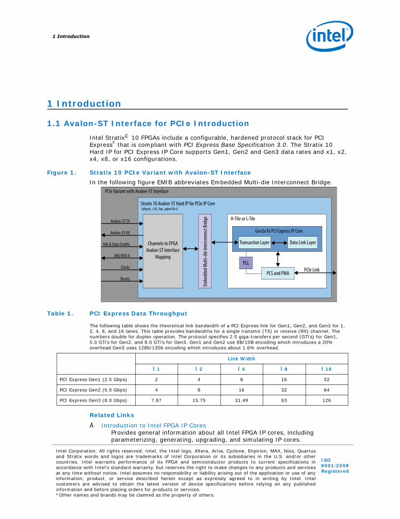
Intel Stratix® 10 FPGAs include a configurable, hardened protocol stack for PCIExpress® that is compliant with PCI Express Base Specification 3.0. The Stratix 10Hard IP for PCI Express IP Core supports Gen1, Gen2 and Gen3 data rates and x1, x2,x4, x8, or x16 configurations.
Figure 1. Stratix 10 PCIe Variant with Avalon-ST InterfaceIn the following figure EMIB abbreviates Embedded Multi-die Interconnect Bridge.
Channels to FPGAAvalon-ST Interface
MappingPLL
Embe
dded
Mult
i-die
Inte
rconn
ect B
ridge
Stratix 10 Avalon-ST Hard IP for PCIe IP Core (altpcie_s10_hip_pipen1b.v)
PCIe Variant with Avalon-ST Interface
H-Tile or L-Tile
PCIe Link
Gen3x16 PCI Express IP Core
Data Link LayerTransaction Layer
Avalon-ST TX
Avalon-ST RX
Hdr & Data Credits
MSI/MSI-X
Clocks
ResetsPCS and PMA
Table 1. PCI Express Data Throughput
The following table shows the theoretical link bandwidth of a PCI Express link for Gen1, Gen2, and Gen3 for 1,2, 4, 8, and 16 lanes. This table provides bandwidths for a single transmit (TX) or receive (RX) channel. Thenumbers double for duplex operation. The protocol specifies 2.5 giga-transfers per second (GT/s) for Gen1,5.0 GT/s for Gen2, and 8.0 GT/s for Gen3. Gen1 and Gen2 use 8B/10B encoding which introduces a 20%overhead.Gen3 uses 128b/130b encoding which introduces about 1.6% overhead.
Link Width
×1 ×2 ×4 ×8 ×16
PCI Express Gen1 (2.5 Gbps) 2 4 8 16 32
PCI Express Gen2 (5.0 Gbps) 4 8 16 32 64
PCI Express Gen3 (8.0 Gbps) 7.87 15.75 31.49 63 126
Related Links
• Introduction to Intel FPGA IP CoresProvides general information about all Intel FPGA IP cores, includingparameterizing, generating, upgrading, and simulating IP cores.
1 Introduction
Intel Corporation. All rights reserved. Intel, the Intel logo, Altera, Arria, Cyclone, Enpirion, MAX, Nios, Quartusand Stratix words and logos are trademarks of Intel Corporation or its subsidiaries in the U.S. and/or othercountries. Intel warrants performance of its FPGA and semiconductor products to current specifications inaccordance with Intel's standard warranty, but reserves the right to make changes to any products and servicesat any time without notice. Intel assumes no responsibility or liability arising out of the application or use of anyinformation, product, or service described herein except as expressly agreed to in writing by Intel. Intelcustomers are advised to obtain the latest version of device specifications before relying on any publishedinformation and before placing orders for products or services.*Other names and brands may be claimed as the property of others.
ISO9001:2008Registered

• Generating a Combined Simulator Setup ScriptCreate simulation scripts that do not require manual updates for software or IPversion upgrades.
• Project Management Best PracticesGuidelines for efficient management and portability of your project and IP files.
• Creating a System QsysProvides information about the Qsys system integration tool that simplifies thetasks of defining and integrating customized IP cores.
1.2 Features
New features in the Quartus Prime Pro v17.1 Stratix 10 ES Editions Software:
• Support for the H-Tile transceiver for up to Gen3 x8 configurations. Refer toTransceiver Tiles for additional information.
• Design examples using the H-Tile available in the Quartus® Prime Pro Editioninstallation directory.
• Support for a Gen3 x16 simulation model that you can use in an Avery testbench.The Avery testbench simulates all 16 lanes. For more information about the Averytestbench, refer to AN-811: Using the Avery BFM for PCI Express Gen3x16Simulation on Intel Stratix 10 Devices. The Intel® simulation testbench supportsGen3 x16 variants by downtraining to Gen3 x8.
The Avalon-ST Stratix 10 Hard IP for PCI Express IP Core supports the followingfeatures:
• Complete protocol stack including the Transaction, Data Link, and Physical Layersimplemented as hard IP.
• ×1, ×2, ×4, ×8 and ×16 configurations with Gen1, Gen2, or Gen3 lane rates forNative Endpoints.
• Avalon®-ST 256-bit interface to the Application Layer.
• Instantiation as a stand-alone IP core from the Quartus Prime Pro Edition IPCatalog or as part of a system design in Qsys.
• Dynamic design example generation.
• PHY interface for PCI Express (PIPE) or serial interface simulation using IEEEencrypted models.
• Testbench bus functional model (BFM) supporting x1, x2, x4, and x8configurations. The x16 configuration downtrains to x8 for Intel (internallycreated) testbench. Alternatively, the Avery testbench that supports allconfigurations is available for a licensing fee.
• Dedicated 69.5 kilobyte (KB) receive buffer.
• End-to-end cyclic redundancy check (ECRC).
Related Links
• Transceiver Tiles on page 10
• AN-811: Using the Avery BFM for PCI Express Gen3x16 Simulation on Intel Stratix10 Devices
1 Introduction
Intel® Stratix® 10 Avalon-ST Interface for PCIe Solutions User Guide7

1.3 Release Information
Table 2. Hard IP for PCI Express Release Information
Item Description
Version Quartus Prime Pro v17.1 Stratix 10 ES Editions Software
Release Date May 2017
Ordering Codes No ordering code is required
Related Links
Timing and Power ModelsReports the default device support levels in the current version of the QuartusPrime Pro Edition software.
1.4 Device Family Support
The following terms define device support levels for Intel FPGA IP cores:
• Advance support—the IP core is available for simulation and compilation for thisdevice family. Timing models include initial engineering estimates of delays basedon early post-layout information. The timing models are subject to change assilicon testing improves the correlation between the actual silicon and the timingmodels. You can use this IP core for system architecture and resource utilizationstudies, simulation, pinout, system latency assessments, basic timing assessments(pipeline budgeting), and I/O transfer strategy (data-path width, burst depth, I/Ostandards tradeoffs).
• Preliminary support—the IP core is verified with preliminary timing models forthis device family. The IP core meets all functional requirements, but might still beundergoing timing analysis for the device family. It can be used in productiondesigns with caution.
• Final support—the IP core is verified with final timing models for this devicefamily. The IP core meets all functional and timing requirements for the devicefamily and can be used in production designs.
Table 3. Device Family Support
Device Family Support Level
Stratix 10 Advance support.The Quartus Prime Pro v17.1 Stratix 10 ES Editions Software supports simulation and compilation.Programmer Object File (.pof) support is available for up to Gen3 x8 with an *.ini file.
Other device families No support.Refer to the Intel PCI Express Solutions web page on the Intel website for support information onother device families.
Related Links
• Timing and Power ModelsReports the default device support levels in the current version of the QuartusPrime Pro Edition software.
• PCI Express Solutions Web Page
1 Introduction
Intel® Stratix® 10 Avalon-ST Interface for PCIe Solutions User Guide8
1.5 Recommended Speed Grades
Table 4. Stratix 10 Recommended Speed Grades for All Avalon-ST Widths andFrequenciesThe recommended speed grades are for production parts.
Lane Rate Link Width Interface Width Application ClockFrequency (MHz)
RecommendedSpeed Grades
Gen1 x1, x2, x4, x8, x16 256 bits 125 –1, –2, -3
Gen2 x1, x2, x4, x8 256 bits 125 –1, –2, -3
Gen2 x16 256 bits 250 –1, –2, -3
Gen3
x1, x2, x4 256 bits 125 –1, –2, -3
x8 256 bits 250 –1, –2 , -3
x16 256 bits 500 –1, –2
1.6 Performance and Resource Utilization
Because the PCIe protocol stack is implemented in hardened logic, it uses no coredevice resources (no ALMs and no embedded memory).
Related Links
Running the FitterFor information on Fitter constraints.
1 Introduction
Intel® Stratix® 10 Avalon-ST Interface for PCIe Solutions User Guide9

1.7 Transceiver Tiles
Stratix 10 introduces several transceiver tile variants to support a wide variety ofprotocols.
Figure 2. Stratix 10 Transceiver Tile Block Diagram
Transceiver Tile (24 Channels) E-Tile
L-Tile and H-Tile
Package Substrate
4
x 10
0GE
EMIB
XCVR
Bank
(6 Ch
anne
ls)
Trans
ceive
r PLL
s
XCVR
Ba
nk(6
Chan
nels)
XCVR
Bank
(6 Ch
anne
ls)PC
Ie H
ard I
P
Refer
ence
Cloc
k Net
work
Clock
Net
work
XCVR
Bank
(6 Ch
anne
ls)
Transceiver Tile (24 Channels) E-Tile
4
x 10
0GE
EMIB
Transceiver Tile (24 Channels) L-Tile/ H-Tile
PCIe
Gen3
Har
d IP
EMIB
®Tra
nsce
iver P
LLs
100G
Ethe
rnet
Har
d IP
Refer
ence
Cloc
k Net
work
Clock
Net
work
Trans
ceive
rs (2
4 Cha
nnels
)
E-Tile
Table 5. Transceiver Tiles Channel Types
Tile Channel TypeChannel Capability
Channel Hard IP accessChip-to-Chip Backplane
L-Tile GX 17.4Gbps (NRZ) 12.5 Gbps (NRZ) PCIe Gen3x16
H-TileGX 17.4 Gbps (NRZ) 17.4 Gbps (NRZ) PCIe Gen3x16
GXT 28.3 Gbps (NRZ) 28.3 Gbps (NRZ) N/A
E-Tile GXE30 Gbps (NRZ),56 Gbps (PAM-4)
30 Gbps (NRZ),56 Gbps (PAM-4)
100G Ethernet
L-Tile and H-Tile
Both L and H transceiver tiles contain four transceiver banks-with a total of 24 duplexchannels, eight ATX PLLs, eight fPLLs, eight CMU PLLs, a PCIe Hard IP block, andassociated input reference and transmitter clock networks. L and H transceiver tilesalso include 10GBASE-KR/40GBASE-KR4 FEC block in each channel.
L-Tiles have transceiver channels that support up to 17.4 Gbps chip-to-chip or12.5Gbps backplane applications. H-Tiles have transceiver channels to support 28Gbpsapplications. H-Tile channels support fast lock-time for Gigabit-capable passive opticalnetwork (GPON).
Stratix GX/SX devices incorporate L-Tiles or H-Tiles. Package migration is availablewith Stratix 10 GX/SX from bL-Tileb to bL-Tileb variants. In addition, device migrationbetween an L-Tile equipped Stratix 10 GX device and an Stratix 10 GX device issupported.
1 Introduction
Intel® Stratix® 10 Avalon-ST Interface for PCIe Solutions User Guide10

E-Tile
E-Tiles are designed to support 56 Gbps with PAM-4 signaling or up to 30 Gbpsbackplane with NRZ signaling. E-Tiles do not include any PCIe Hard IP blocks.
1.8 PCI Express IP Core Package Layout
Stratix 10 devices have high-speed transceivers that are implemented on separatetransceiver tiles. The transceiver tiles are located on the left and right sides of thedevice.
Each 24-channel transceiver tile includes one Gen3 x16 PCIe IP Core implemented inhardened logic. The following figures show the layout of PCIe IP cores in Stratix 10devices. Both L- and H-tiles are orange. E-tiles are green.
Figure 3. Stratix 10 GX/SX Devices with 4 PCIe Hard IP Cores and 96 TransceiverChannels
Transceiver Tile(24 Channels)
Transceiver Tile(24 Channels)
Transceiver Tile(24 Channels)
Transceiver Tile(24 Channels)
Package SubstrateEM
IBEM
IB
EMIB
EMIB
Core Fabric
®
GX/SX 1650 UF50 (F2397B)GX/SX 2100 UF50 (F2397B)GX/SX 2500 UF50 (F2397B)GX/SX 2800 UF50 (F2397B)PC
Ie H
IP
PCIe
HIP
PCIe
HIP
PC
Ie H
IP
Figure 4. Stratix 10 GX/SX Devices with 2 PCIe Hard IP Cores and 48 TransceiverChannels
Package Substrate
EMIB
EMIB
Core Fabric
®
GX/SX 850 NF43 (F1760A)GX/SX 1100 NF43 (F1760A)GX/SX 1650 NF43 (F1760A)GX/SX 2100 NF43 (F1760A)GX/SX 2500 NF43 (F1760A)GX/SX 2800 NF43 (F1760A)GX/SX 850 NF48 (F2112A)GX/SX 1100 NF48 (F2112A)
Transceiver Tile(24 Channels)
Transceiver Tile(24 Channels)
PCIe
HIP
PCIe
HIP
1 Introduction
Intel® Stratix® 10 Avalon-ST Interface for PCIe Solutions User Guide11
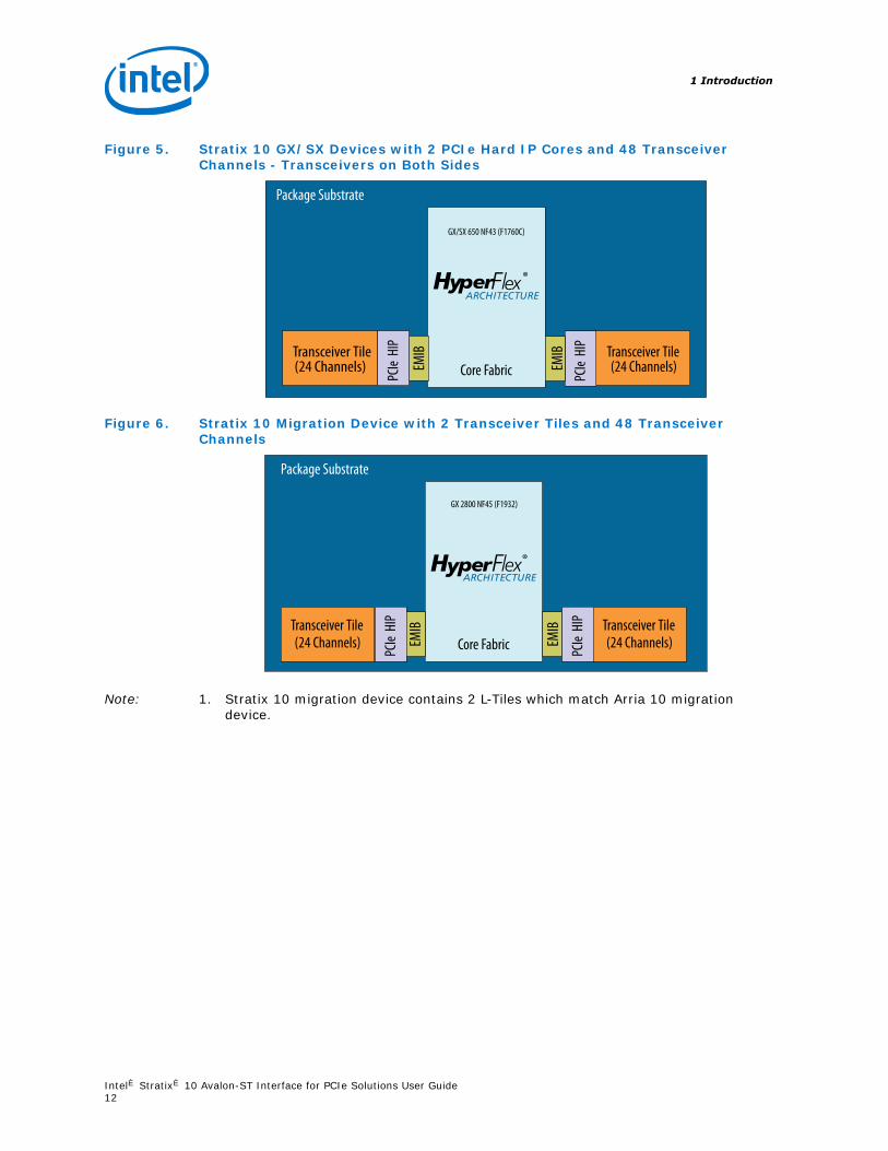
Figure 5. Stratix 10 GX/SX Devices with 2 PCIe Hard IP Cores and 48 TransceiverChannels - Transceivers on Both Sides
Package Substrate
Core Fabric
®
GX/SX 650 NF43 (F1760C)
(24 Channels)(24 Channels) EMIB
PCIe
HIP
PCIe
HIP
Transceiver TileTransceiver Tile
EMIB
Figure 6. Stratix 10 Migration Device with 2 Transceiver Tiles and 48 TransceiverChannels
Transceiver Tile(24 Channels)
Transceiver Tile(24 Channels)
Package Substrate
EMIB
EMIB
Core Fabric
®
GX 2800 NF45 (F1932)
PCIe
HIP
PCIe
HIP
Note: 1. Stratix 10 migration device contains 2 L-Tiles which match Arria 10 migrationdevice.
1 Introduction
Intel® Stratix® 10 Avalon-ST Interface for PCIe Solutions User Guide12
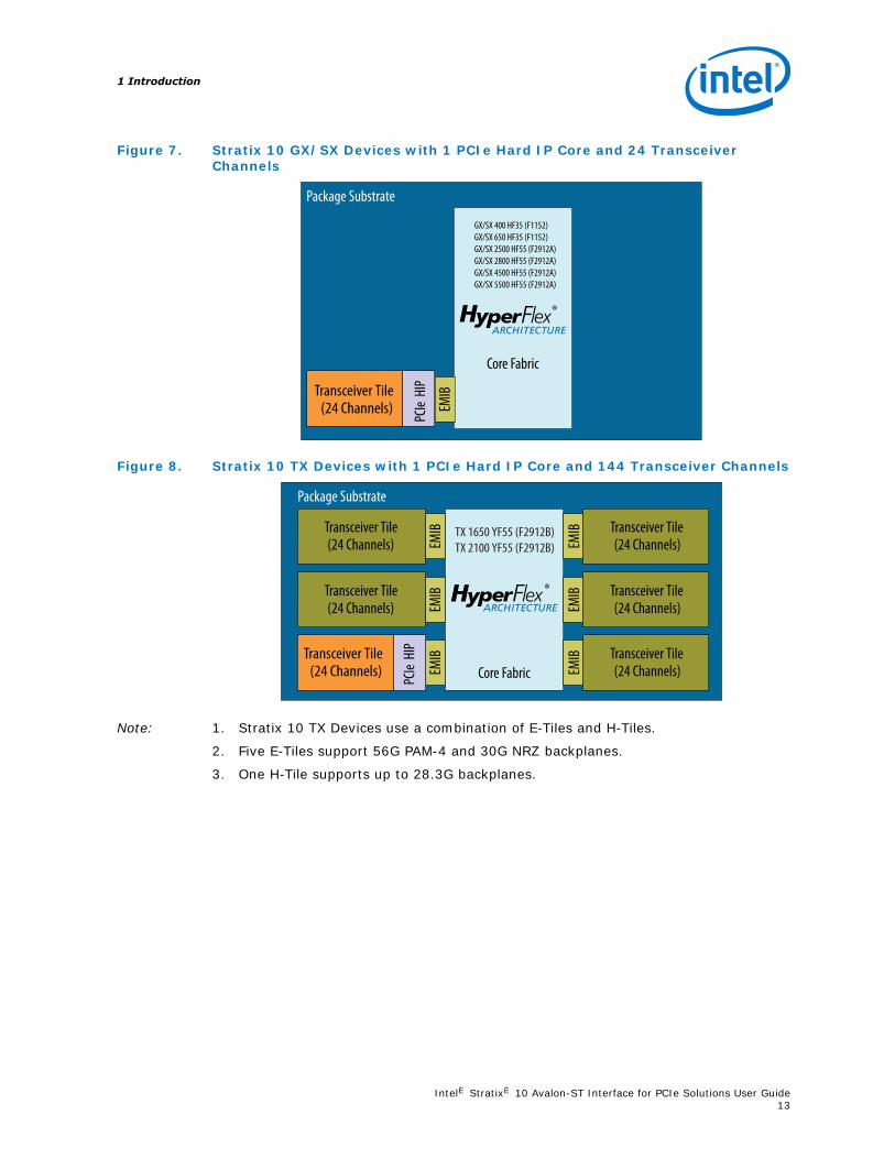
Figure 7. Stratix 10 GX/SX Devices with 1 PCIe Hard IP Core and 24 TransceiverChannels
Package Substrate
Core Fabric
®
GX/SX 400 HF35 (F1152)GX/SX 650 HF35 (F1152)GX/SX 2500 HF55 (F2912A)GX/SX 2800 HF55 (F2912A)GX/SX 4500 HF55 (F2912A)GX/SX 5500 HF55 (F2912A)
Transceiver Tile(24 Channels) PC
Ie H
IP
EMIB
Figure 8. Stratix 10 TX Devices with 1 PCIe Hard IP Core and 144 Transceiver Channels
Transceiver Tile(24 Channels)
Transceiver Tile(24 Channels)
Transceiver Tile(24 Channels)
Transceiver Tile(24 Channels)
Transceiver Tile(24 Channels)
Package Substrate
EMIB
EMIB
EMIB
EMIB
EMIB
EMIB
Core Fabric
®
TX 1650 YF55 (F2912B)TX 2100 YF55 (F2912B)
Transceiver Tile(24 Channels) PC
Ie H
IP
Note: 1. Stratix 10 TX Devices use a combination of E-Tiles and H-Tiles.
2. Five E-Tiles support 56G PAM-4 and 30G NRZ backplanes.
3. One H-Tile supports up to 28.3G backplanes.
1 Introduction
Intel® Stratix® 10 Avalon-ST Interface for PCIe Solutions User Guide13

Figure 9. Stratix 10 TX Devices with 1 PCIe Hard IP Core and 96 Transceiver Channels
Transceiver Tile(24 Channels)
Transceiver Tile(24 Channels)
Transceiver Tile(24 Channels)
Transceiver Tile(24 Channels)
Package Substrate
EMIB
EMIB
EMIB
EMIB
Core Fabric
®
TX 1650 UF50 (F2397C)TX 2100 UF50 (F2397C)TX 2500 UF50 (F2397C)TX 2800 UF50 (F2397C)
PCIe
HIP
Note: 1. Stratix 10 TX Devices use a combination of E-Tiles and H-Tiles.
2. Three E-Tiles support 56G PAM-4 and 30G NRZ backplanes.
3. One H-Tile supports up to 28.3G backplanes.
Figure 10. Stratix 10 TX Devices with 2 PCIe Hard IP Cores and 72 Transceiver Channels
Transceiver Tile(24 Channels)
Transceiver Tile(24 Channels)
Transceiver Tile(24 Channels)
Package Substrate
EMIB
EMIB
EMIB
Core Fabric
®
TX 1650 SF48 (F2212B)TX 2100 SF48 (F2212B)TX 2500 SF48 (F2212B)TX 2800 SF48 (F2212B)
PCIe
HIP
PC
Ie H
IP
Note: 1. Stratix 10 TX Devices use a combination of E-Tiles and H-Tiles.
2. One E-Tile support 56G PAM-4 and 30G NRZ backplanes.
3. Two H-Tiles supports up to 28.3G backplanes.
Related Links
Stratix 10 GX/SX Device OverviewFor more information about Stratix 10 devices.
1 Introduction
Intel® Stratix® 10 Avalon-ST Interface for PCIe Solutions User Guide14

1.9 Channel Availability
PCIe Hard IP Channel Restrictions
Each transceiver tile contains a PCIe Hard IP block. The following table and figureshow the possible PCIe Hard IP channel configurations, the number of unusablechannels, and the number of channels available for other protocols. For example, aPCIe x4 variant uses 4 channels and 4 additional channels are unusable.
Table 6. Unusable Channels
PCIe Hard IP Configuration Number of Unusable Channels Number of Channels Available forOther Protocols
PCIe x1 7 16
PCIe x2 6 16
PCIe x4 4 16
PCIe x8 0 16
PCIe x16 16 8
Figure 11. PCIe Hard IP Channel Configurations Per Transceiver Tile
PCIe Hard IP x1
7 ChannelsUnusable
PCIe x1
PCIe Hard IP x2
6 ChannelsUnusable
PCIe x2
PCIe Hard IP x4
4 ChannelsUnusable
PCIe x4
PCIe Hard IP x8
PCIe x8
PCIe Hard IP x16
PCIe x16
Transceiver Tile Transceiver Tile Transceiver Tile Transceiver Tile Transceiver Tile0 0 0 0 0
15
23 23 23 23 23
8 8 87 7
8
134
1
7
2
7
16 ChannelsUsable
16 ChannelsUsable
16 ChannelsUsable
16 ChannelsUsable
8 ChannelsUsable
16
The table below maps all transceiver channels to PCIe Hard IP channels in availabletiles.
Table 7. PCIe Hard IP channel mapping across all tiles
Tile ChannelSequence
PCIe Hard IPChannel
Indexwithin I/O
Bank
Bottom LeftTile BankNumber
Top Left TileBank Number
Bottom RightTile BankNumber
Top Right TileBank Number
23 N/A 5 1F 1N 4F 4N
22 N/A 4 1F 1N 4F 4N
21 N/A 3 1F 1N 4F 4N
continued...
1 Introduction
Intel® Stratix® 10 Avalon-ST Interface for PCIe Solutions User Guide15

Tile ChannelSequence
PCIe Hard IPChannel
Indexwithin I/O
Bank
Bottom LeftTile BankNumber
Top Left TileBank Number
Bottom RightTile BankNumber
Top Right TileBank Number
20 N/A 2 1F 1N 4F 4N
19 N/A 1 1F 1N 4F 4N
18 N/A 0 1F 1N 4F 4N
17 N/A 5 1E 1M 4E 4M
16 N/A 4 1E 1M 4E 4M
15 15 3 1E 1M 4E 4M
14 14 2 1E 1M 4E 4M
13 13 1 1E 1M 4E 4M
12 12 0 1E 1M 4E 4M
11 11 5 1D 1L 4D 4L
10 10 4 1D 1L 4D 4L
9 9 3 1D 1L 4D 4L
8 8 2 1D 1L 4D 4L
7 7 1 1D 1L 4D 4L
6 6 0 1D 1L 4D 4L
5 5 5 1C 1K 4C 4K
4 4 4 1C 1K 4C 4K
3 3 3 1C 1K 4C 4K
2 2 2 1C 1K 4C 4K
1 1 1 1C 1K 4C 4K
0 0 0 1C 1K 4C 4K
PCIe Soft IP Channel Usage
PCI Express soft IP PIPE-PHY cores available from third-party vendors are not subjectto the channel usage restrictions described above. Refer to Intel FPGA ➤ Products➤ Intellectual Property for more information about soft IP cores for PCI Express.
1 Introduction
Intel® Stratix® 10 Avalon-ST Interface for PCIe Solutions User Guide16

2 Quick Start GuideUsing Qsys Pro, you can generate a PIO design example for the Avalon-ST Stratix 10Hard IP for PCI Express IP core. The generated design example reflects theparameters that you specify. The PIO example transfers data from a host processor toa target device. It is appropriate for low-bandwidth applications. This design exampleautomatically creates the files necessary to simulate and compile in the Quartus PrimePro software. You can download the compiled design to the Stratix 10 DevelopmentBoard or your own custom hardware.
In addition to the dynamically generated design examples, you can download staticdesign examples from the following directories:
• For the L-Tile transceiver: <install_dir>/ip/altera/altera_pcie/altera_pcie_s10_ed/example_design/s10.
• For the H-Tile transceiver: <install_dir>/ip/altera/altera_pcie/altera_pcie_s10_ed/example_design/s10_htile
The static design examples are available for simulation and compilation.
Figure 12. Development Steps for the Design Example
DesignExample
Generation
Compilation(Simulator)
FunctionalSimulation
Compilation(Quartus Prime)
HardwareTesting
2 Quick Start Guide
Intel Corporation. All rights reserved. Intel, the Intel logo, Altera, Arria, Cyclone, Enpirion, MAX, Nios, Quartusand Stratix words and logos are trademarks of Intel Corporation or its subsidiaries in the U.S. and/or othercountries. Intel warrants performance of its FPGA and semiconductor products to current specifications inaccordance with Intel's standard warranty, but reserves the right to make changes to any products and servicesat any time without notice. Intel assumes no responsibility or liability arising out of the application or use of anyinformation, product, or service described herein except as expressly agreed to in writing by Intel. Intelcustomers are advised to obtain the latest version of device specifications before relying on any publishedinformation and before placing orders for products or services.*Other names and brands may be claimed as the property of others.
ISO9001:2008Registered

2.1 Design Components
Figure 13. Block Diagram for the Qsys PIO Design Example Simulation Testbench
Avalon-STdata
Generated PCIeEndpoint
Variant (DUT)
On-ChipMemory
(MEM)
PCIe Example Design
PIO Application(Memory for Gen3 x16)
hip_serial
hip_pipe
OR
Root Port BFM(RP_BFM)
PCIe Example Design Simulation Testbench
Avalon-MMdata
Figure 14. Important Interfaces and Signals in the Stratix 10 PCIe PIO Design Example
tx_st_hip
rx_st_hip
reset
clk
APPS
hprxms1
reset1
clk1
On-Chip Memory(RAM or ROM)
NPOR
PERST#
REF_CLK
tx_st
rx_st
nreset_status
coreclkout_hip
DUT(Stratix 10 Hard IP
for PCI Express)Serial/PIPE
Interface
Avalon-MM Interface
256 256
256
2 Quick Start Guide
Intel® Stratix® 10 Avalon-ST Interface for PCIe Solutions User Guide18

2.2 Directory Structure
Figure 15. Directory Structure for the Generated Design Example
pcie_s10_hip_0_example_design
pcie_example_design
<top-level design files>
pcie_example_design_tb
pcie_example_design_tb
<simulator script>
testbench component
sim
<simulator>
<simulator script>
<simulator>
ip
pcie_example_design
<design component>.ip
<design component 1>
internal component
sim
synth
<design component <n>
internal component
sim
synth
pcie_example_design.qpf
pcie_example_design.qsf
pcie_example_design.sdc
pcie_example_design.qsys
ip
sim
synth
2 Quick Start Guide
Intel® Stratix® 10 Avalon-ST Interface for PCIe Solutions User Guide19

2.3 Generating the Design
Figure 16. Procedure
Start ParameterEditor
Specify IP Variationand Select Device
SelectDesign Parameters
InitiateDesign Generation
Specify Example Design
Follow these steps to generate your design:
1. In the Quartus Prime Pro software, create a new project (File ➤ New ProjectWizard).
2. Specify the Directory, Name, and Top-Level Entity.
3. For Project Type, accept the default value, Empty project.
4. For Add Files, click Next.
5. For Family, Device & Board Settings, under Family, select Stratix 10(GX/SX) and the Target Device for your design. The Stratix 10 Development Kitincludes the 1SG280HU3F50E3VG device. The following devices are compatiblewith the 1SG280HU3F50E3VG device:
• 1SG280LU3F50E3VGS1
• 1SG280LU3F50E3VG
• 1SG280HU3F50E3VGS1
• 1SG280HU3F50E3VG
In the current release, dynamic design example generation overwrites yourselection with the 1SG280HU3F50E3VG device. Consequently, you can downloadyour design to the Stratix 10 Development Kit.
6. Click Finish.
7. Select Tools ➤ Qsys Pro.
8. For Qsys System or IP Variant, click + and specify a File name. Click Create.Click create again.
9. On the Qsys System Contents tab, delete the clock_in and reset_incomponents that appear by default.
10. In the IP Catalog locate and add the Avalon-ST Stratix 10 Hard IP for PCIExpress.
11. On the IP Settings tabs, specify the parameters for your IP variation.
12. On the System Contents tab, connect refclk to coreclkout_hip.
13. On the Example Designs tab, select the PIO design.
2 Quick Start Guide
Intel® Stratix® 10 Avalon-ST Interface for PCIe Solutions User Guide20

Figure 19. Example Design Tab
Initiates DesignGeneration
14. For Example Design Files, select the Simulation and Synthesis options.
15. For Generated HDL Format, only Verilog is available.
16. For Target Development Kit select the NONE option. Although the Stratix 10Development Kit is not listed, it is available in limited quantities to Betacustomers. Contact Intel.
17. Click the Generate Example Design button. The software generates all filesnecessary to run simulations. Click Close when generation completes.
18. Click Finish.
19. Save your .ip file when prompted.
20. The prompt, Recent changes have not been generated. Generate now?,allows you to create files for simulation and synthesis. Click No to continue tosimulate the design example you just generated.
2.4 Simulating the Design
Figure 20. Procedure
Change to Testbench Directory
Run<Simulation Script>
AnalyzeResults
1. Change to the testbench simulation directory.
2. Run the simulation script for the simulator of your choice. Refer to the table below.
3. Analyze the results.
2 Quick Start Guide
Intel® Stratix® 10 Avalon-ST Interface for PCIe Solutions User Guide21

Table 8. Steps to Run Simulation
Simulator Working Directory Instructions
ModelSim* <example_design>/pcie_example_design_tb/pcie_example_design_tb/sim/mentor/
1. do msim_setup.tcl
2. ld_debug
3. run -all
4. A successful simulation ends with the followingmessage, "Simulation stopped due tosuccessful completion!"
VCS* <example_design>/pcie_example_design_tb/pcie_example_design_tb/sim/synopsys/vcs
1. sh vcs_setup.shUSER_DEFINED_SIM_OPTIONS=""
2. A successful simulation ends with the followingmessage, "Simulation stopped due tosuccessful completion!"
This testbench simulates up to x8 variants. It supports x16 variants by down-trainingto x8. To simulate all lanes of a x16 variant, you can create a simulation model inQsys to use in an Avery testbench. For more information refer to AN-811: Using theAvery BFM for PCI Express Gen3x16 Simulation on Intel Stratix 10 Devices.
The automatically generated testbench completes the following tasks:
• Host allocation of memory
• Reads the DMA read status register
• Sets up two DMA write descriptors in host memory and performs DMA writes
• Checks the status for the DMA writes
• Verifies the data for the DMA writes
The simulation reports, "Simulation stopped due to successful completion" if no errorsoccur.
2 Quick Start Guide
Intel® Stratix® 10 Avalon-ST Interface for PCIe Solutions User Guide22
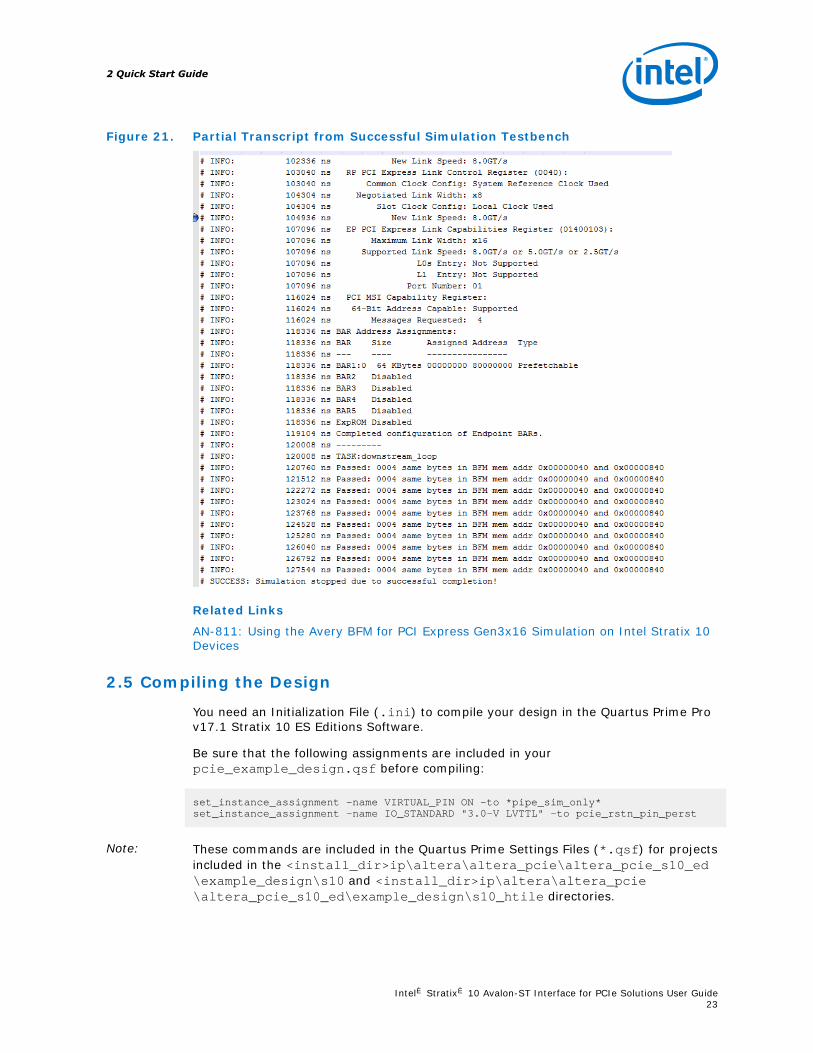
Figure 21. Partial Transcript from Successful Simulation Testbench
Related Links
AN-811: Using the Avery BFM for PCI Express Gen3x16 Simulation on Intel Stratix 10Devices
2.5 Compiling the Design
You need an Initialization File (.ini) to compile your design in the Quartus Prime Prov17.1 Stratix 10 ES Editions Software.
Be sure that the following assignments are included in yourpcie_example_design.qsf before compiling:
set_instance_assignment -name VIRTUAL_PIN ON -to *pipe_sim_only*set_instance_assignment -name IO_STANDARD "3.0-V LVTTL" -to pcie_rstn_pin_perst
Note: These commands are included in the Quartus Prime Settings Files (*.qsf) for projectsincluded in the <install_dir>ip\altera\altera_pcie\altera_pcie_s10_ed\example_design\s10 and <install_dir>ip\altera\altera_pcie\altera_pcie_s10_ed\example_design\s10_htile directories.
2 Quick Start Guide
Intel® Stratix® 10 Avalon-ST Interface for PCIe Solutions User Guide23

1. On the Processing menu, select Start Compilation.
2. When compilation completes, click Assembler (Generate programming files)to generate an SRAM Object File (.sof).
3. After successfully compiling your design, program the targeted device with theProgrammer and verify the design in hardware.
2 Quick Start Guide
Intel® Stratix® 10 Avalon-ST Interface for PCIe Solutions User Guide24

3 Interface OverviewThe PCI Express Base Specification 3.0 defines a packet interface for communicationbetween a Root Port and an Endpoint. When you select the Avalon-ST interface,Transaction Layer Packets (TLP) transfer data between the Root Port and an Endpointusing the Avalon-ST TX and RX interfaces. The interfaces are named from the point-of-view of the user logic.
Figure 22. Stratix 10 Top-Level Interfaces
Channels to FPGAAvalon-ST Interface
MappingPLL
Embe
dded
Mult
i-die
Inte
rconn
ect B
ridge
Stratix 10 Avalon-ST Hard IP for PCIe IP Core (altpcie_s10_hip_pipen1b.v)
PCIe Variant with Avalon-ST Interface
H-Tile or L-Tile
PCIe Link
Gen3x16 PCI Express IP Core
Data Link LayerTransaction Layer
Avalon-ST TX
Avalon-ST RX
Hdr & Data Credits
MSI/MSI-X
Clocks
ResetsPCS and PMA
The following figures show the PCIe hard IP Core top-level interfaces and theconnections to the Application Layer and system.
3 Interface Overview
Intel Corporation. All rights reserved. Intel, the Intel logo, Altera, Arria, Cyclone, Enpirion, MAX, Nios, Quartusand Stratix words and logos are trademarks of Intel Corporation or its subsidiaries in the U.S. and/or othercountries. Intel warrants performance of its FPGA and semiconductor products to current specifications inaccordance with Intel's standard warranty, but reserves the right to make changes to any products and servicesat any time without notice. Intel assumes no responsibility or liability arising out of the application or use of anyinformation, product, or service described herein except as expressly agreed to in writing by Intel. Intelcustomers are advised to obtain the latest version of device specifications before relying on any publishedinformation and before placing orders for products or services.*Other names and brands may be claimed as the property of others.
ISO9001:2008Registered

Figure 23. Connections: User Application to Stratix 10 Avalon-ST Hard IP for PCIe IPCore
PCIeRX Port
Avalon-STMaster
rx_st_*
PCIeTX Port
Avalon-STSlave
tx_st_*
tx_ph_cdts[7:0]tx_pd_cdts[11:0]tx_nph_cdts[7:0]tx_npd_cdts[11:0]tx_cplh_cdts[7:0]tx_cpld_cdts[11:0]tx_hdr_cdts_consumedtx_data_cdts_consumedtx_cdts_type[1:0]tx_cdts_data_value[1:0]
PCIe Clocks and Resets
coreclkout_hip
refclk
nporcurrent_speed[1:0]
pin_perstpld_clk_inusepld_core_readyreset_statusserdes_pll_locked
PCIe MSI Interface
app_msi_*app_int_stsint_status[3:0]int_status_common[2:0]
PCIe Configuration Space Signals
PCIe Configuration Extension Bus
ceb_*
app_err_*
tl_cfg_*
PCIe Hard IP Status Interface
derr_*int_status[3:0]int_status_common[2:0]lane_act[4:0]link_upltssmstate[5:0]rx_par_errtx_par_err
Application RX Interface
Avalon-STSlave
Application TX Interface
Avalon-STMaster
Application Clocks and Reset Interface
Application MSI Interface
Application Configuration Space Interface
Application Configuration Extension Interface
Application HIP Status Interface
Avalon-ST Interface to the PCIe IP Core Application and System Interfaces
3 Interface Overview
Intel® Stratix® 10 Avalon-ST Interface for PCIe Solutions User Guide26

Figure 24. Connections: PCIe Link and Reconfiguration, Power and Test Interfaces
Hard IP Reconfiguration
(Optional)
Avalon-MMSlave
hip_reconfig_*
PCIe Power Management
pm_*
apps_pm_xmt_pmeapps_ready_entr_123apps_pm_xmt_turnoffapp_init_rstapp_xfer_pending
PCIe Serial Data Interfacerx_in
PCIe PIPE (Simulation Only)
Receive Data
tx_out[<n>-1:0]
[<n>-1:0]
tx *powerdown[1:0]
rate[1:0]rxpolarity
currentrxpreset0[2:0]
currentcoeff0[17:0]rxeqevalrxeqinprogress
rx *
phystatus0
dirfeedback[5:0]
simu_mode_pipesim_pipe_pclk_in
sim_pipe_mask_tx_pll
sim_pipe_rate [1:0]
sim_ltssmstate [5:0]
Hard IP Reconfiguation
(Optional)
Avalon-MMMaster
Application Power Management Interface
test_in[66:0]
testin_zero Application Test Interface
PCIe IP Core Interfaces Application InterfacesPCIe Link
Transmit Data
PCIe Test Interface
The following sections introduce these interfaces. Refer to the Interfaces section in theBlock Description chapter for detailed descriptions and timing diagrams.
Avalon-ST RX
The Transaction Layer transfers TLPs to the Application on this 256-bit interface. TheApplication must assert rx_st_ready before transfers can begin. The latency on thisinterface includes the three-cycle ready latency and the latency of the EmbeddedMulti-die Interconnect Bridge (EMIB) for a total of 17 cycles. Once rx_st_readydeasserts, rx_st_valid will deassert within 17 cycles. Once rx_st_readyreasserts, rx_st_valid will resume data transfer within 17 cycles. To achieve thebest performance the Application must include a receive buffer large enough to avoidthe deassertion of rx_st_ready. Refer to Avalon-ST RX Interface for moreinformation.
Note: Throughout this user guide the terms Application and Application Layer refer to thecustomer logic that interfaces with the PCIe Transaction Layer.
3 Interface Overview
Intel® Stratix® 10 Avalon-ST Interface for PCIe Solutions User Guide27

Avalon-ST TX
The Application transmits TLPs to the Transaction Layer of the IP core on this 256-bitinterface. The Transaction Layer must assert tx_st_ready before transmissionbegins. Transmission must be continuous when tx_st_ready is asserted. The readylatency is three coreclkout_hip cycles. If tx_st_ready deasserts, the Applicationmust stop transmitting data within three cycles. When tx_st_ready reasserts, theApplication must wait for three clock cycles before resuming data transmission. Formore detailed information about the Avalon-ST interface, refer to Avalon-ST TXInterface. The packet layout is shown in detail in the Block Description chapter.
TX Credit
The Transaction Layer TX interface transmits TLPs in the same order as they werereceived from the Application. To optimize performance, the Application can performcredit-based checking before submitting requests for transmission, allowing theApplication to reorder packets to improve throughput. Application reordering isoptional. The Transaction Layer always performs its own credit check beforetransmitting any TLP.
TX and RX Serial Data
This differential, serial interface is the physical link between a Root Port and anEndpoint. The PCIe IP Core supports 1, 2, 4, 8, or 16 lanes. Each lane includes a TXand RX differential pair. Data is striped across all available lanes.
PIPE
This is a 32-bit parallel interface between the PCIe IP Core and PHY. It carries the TLPdata before it is serialized. It is available for simulation only and provides morevisibility for debugging.
ClocksThe PCI Express Card Electromechanical Specification Revision 2.0 defines the inputreference clock. It is a 100 MHz ±300 ppm. The motherboard drives this clock to thePCIe card. The PCIe card is not required to use the reference clock received from theconnector. However, the PCIe card must provide a 100 MHz ±300 ppm to the refclkinput pin.
Table 9. Application Clock FrequencyThe interface to the Application is fixed at 256 bits; consequently, the Application clock frequency depends onlyon the data rate.
Data Rate Clock Frequency
Gen1 x1, x2, x4, x8, and x16 125 MHz
Gen2 x1, x2, x4, and x8 125 MHz
Gen2 x16 250 MHz
Gen3 x1, x2, and x4 125 MHz
Gen3 x8 250 MHz
Gen3 x16 500 MHz
ResetThe PCIe IP core receives two reset inputs:
3 Interface Overview
Intel® Stratix® 10 Avalon-ST Interface for PCIe Solutions User Guide28

• pin_perst is the active low, edge-triggered reset driven from the PCIemotherboard. Logic on the motherboard autonomously generates this fundamentalreset signal.
• npor is an active low, edge-triggered reset signal. The Application drives thisreset signal.
The PCIe IP core reset logic requires a free-running clock input. This free-runningclock becomes stable after the secure device manager (SDM) block assertsiocsrrdy_dly indicating that the I/O Control and Status registers programming iscomplete.
Reset StatusThis interface indicates when the clocks are stable and FPGA configuration is complete.
Hard IP Status
This optional interface includes the following signals that are useful for debugging
• Link status signals
• Interrupt status signals
• TX and RX parity error signals
• Correctable and uncorrectable error signals
Interrupts
The PCIe IP core support Message Signaled Interrupts (MSI), MSI-X interrupts, andLegacy interrupts. MSI, MSI-X, and legacy interrupts are mutually exclusive.
MSI uses the TLP single dword memory writes to implement interrupts. This interruptmechanism conserves pins because it does not use separate wires for interrupts. Inaddition, the single dword provides flexibility for the data presented in the interruptmessage. The MSI Capability structure is stored in the Configuration Space and isprogrammed using Configuration Space accesses.
The Application generates MSI-X messages which are single dword memory writes.The MSI-X Capability structure points to an MSI-X table structure and MSI-X PBAstructure which are stored in memory. This scheme is different than the MSI capabilitystructure, which contains all the control and status information for the interrupts.
Enable Legacy interrupts by programming the Interrupt Disable bit (bit[10]) ofthe Configuration Space Command to 1'b0. When legacy interrupts are enabled, the IPcore emulates INTx interrupts using virtual wires. The app_int_sts port controlslegacy interrupt generation.
Transaction Layer (TL ) tl_cfg ConfigurationThis interface provides time-domain multiplexed (TD) access to a subset of the valuesstored in the Configuration Space registers.
Hard IP ReconfigurationThis optional Avalon Memory-Mapped (Avalon-MM) interface allows you to dynamicallyupdate the value of read-only Configuration Space registers at run-time. It is availablewhen Enable dynamic reconfiguration of PCIe read-only registers is enabled inthe component GUI.
3 Interface Overview
Intel® Stratix® 10 Avalon-ST Interface for PCIe Solutions User Guide29

Power ManagementSoftware uses the power management interface to control the power managementstate machine. The power management output signals indicate the current powerstate. The IP core supports the two mandatory power states: D0 full power and D3preparation for loss of power. It does not support the optional D1 and D2 low-powerstates.
Related Links
• Avalon-ST RX Interface on page 54The Application Layer receives data from the Transaction Layer of the PCIe IPcore over the Avalon-ST RX interface. This is a 256-bit interface.
• Interfaces on page 52This section describes the top-level interfaces in the Avalon-ST Stratix 10 HardIP for PCIe IP core.
• PCI Express Base Specification 3.0
3 Interface Overview
Intel® Stratix® 10 Avalon-ST Interface for PCIe Solutions User Guide30

4 ParametersThis chapter provides a reference for all the parameters of the Stratix 10 Hard IP forPCI Express IP core.
Table 10. System Settings
Parameter Value Description
ApplicationInterface Type
Avalon-ST Selects the interface to the Application Layer.
Hard IP Mode Gen3x16, 256-bit interface, 500 MHzGen3x8, 256-bit interface, 250 MHzGen3x4, 256-bit interface, 125 MHzGen3x2, 256-bit interface, 125 MHzGen3x1, 256-bit interface, 125 MHz
Gen2x16, 256-bit interface, 250 MHzGen2x8, 256-bit interface, 125 MHzGen2x4, 256-bit interface, 125 MHzGen2x2, 256-bit interface, 125 MHzGen2x1, 256-bit interface, 125 MHz
Gen1x16, 256-bit interface, 125 MHzGen1x8, 256-bit interface, 125 MHzGen1x4, 256-bit interface, 125 MHzGen1x2, 256-bit interface, 125 MHzGen1x1, 256-bit interface, 125 MHz
Selects the following elements:• The lane data rate. Gen1, Gen2, and Gen3 are
supported• The Application Layer interface frequencyThe width of the data interface between the hard IPTransaction Layer and the Application Layerimplemented in the FPGA fabric interface is 256-bit.Note: If the Mode selected is not available for the
configuration chosen, an error message displaysin the Message pane.
Port type Native Endpoint Specifies the port type.The Endpoint stores parameters in the Type 0Configuration Space. Only Native Endpoints aresupported in the Quartus Prime Pro v17.1 Stratix 10 ESEditions.
Related Links
PCI Express Base Specification 3.0
4.1 Stratix 10 Avalon-ST Settings
Table 11. System Settings for PCI Express
Parameter Value Description
Enable Avalon-STreset output port
On/Off When On, the generated reset output port clr_st has the samefunctionality as the hip_ready_n port included in the Hard IP Resetinterface. This option is available for backwards compatibility with Arria® 10devices.
Enable byte parityports onAvalon-STinterface
On/Off When On, the RX and TX datapaths are parity protected. Parity is odd. TheApplication Layer must provide valid byte parity in the Avalon-ST TXdirection.
continued...
4 Parameters
Intel Corporation. All rights reserved. Intel, the Intel logo, Altera, Arria, Cyclone, Enpirion, MAX, Nios, Quartusand Stratix words and logos are trademarks of Intel Corporation or its subsidiaries in the U.S. and/or othercountries. Intel warrants performance of its FPGA and semiconductor products to current specifications inaccordance with Intel's standard warranty, but reserves the right to make changes to any products and servicesat any time without notice. Intel assumes no responsibility or liability arising out of the application or use of anyinformation, product, or service described herein except as expressly agreed to in writing by Intel. Intelcustomers are advised to obtain the latest version of device specifications before relying on any publishedinformation and before placing orders for products or services.*Other names and brands may be claimed as the property of others.
ISO9001:2008Registered
Parameter Value Description
This parameter is only available for the Avalon-ST Stratix 10 Hard IP for PCIExpress.
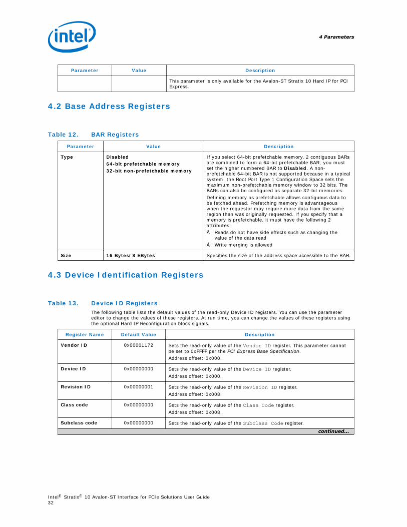
4.2 Base Address Registers
Table 12. BAR Registers
Parameter Value Description
Type Disabled64-bit prefetchable memory32-bit non-prefetchable memory
If you select 64-bit prefetchable memory, 2 contiguous BARsare combined to form a 64-bit prefetchable BAR; you mustset the higher numbered BAR to Disabled. A non-prefetchable 64-bit BAR is not supported because in a typicalsystem, the Root Port Type 1 Configuration Space sets themaximum non-prefetchable memory window to 32 bits. TheBARs can also be configured as separate 32-bit memories.Defining memory as prefetchable allows contiguous data tobe fetched ahead. Prefetching memory is advantageouswhen the requestor may require more data from the sameregion than was originally requested. If you specify that amemory is prefetchable, it must have the following 2attributes:• Reads do not have side effects such as changing the
value of the data read• Write merging is allowed
Size 16 Bytes–8 EBytes Specifies the size of the address space accessible to the BAR.
4.3 Device Identification Registers
Table 13. Device ID RegistersThe following table lists the default values of the read-only Device ID registers. You can use the parametereditor to change the values of these registers. At run time, you can change the values of these registers usingthe optional Hard IP Reconfiguration block signals.
Register Name Default Value Description
Vendor ID 0x00001172 Sets the read-only value of the Vendor ID register. This parameter cannotbe set to 0xFFFF per the PCI Express Base Specification.Address offset: 0x000.
Device ID 0x00000000 Sets the read-only value of the Device ID register.Address offset: 0x000.
Revision ID 0x00000001 Sets the read-only value of the Revision ID register.Address offset: 0x008.
Class code 0x00000000 Sets the read-only value of the Class Code register.Address offset: 0x008.
Subclass code 0x00000000 Sets the read-only value of the Subclass Code register.
continued...
4 Parameters
Intel® Stratix® 10 Avalon-ST Interface for PCIe Solutions User Guide32
Register Name Default Value Description
Address offset: 0x008.
SubsystemVendor ID
0x00000000 Sets the read-only value of Subsystem Vendor ID register in the PCI Type0 Configuration Space. This parameter cannot be set to 0xFFFF per the PCIExpress Base Specification. This value is assigned by PCI-SIG to the devicemanufacturer.Address offset: 0x02C.
Subsystem DeviceID
0x00000000 Sets the read-only value of the Subsystem Device ID register in the PCIType 0 Configuration Space.Address offset: 0x02C
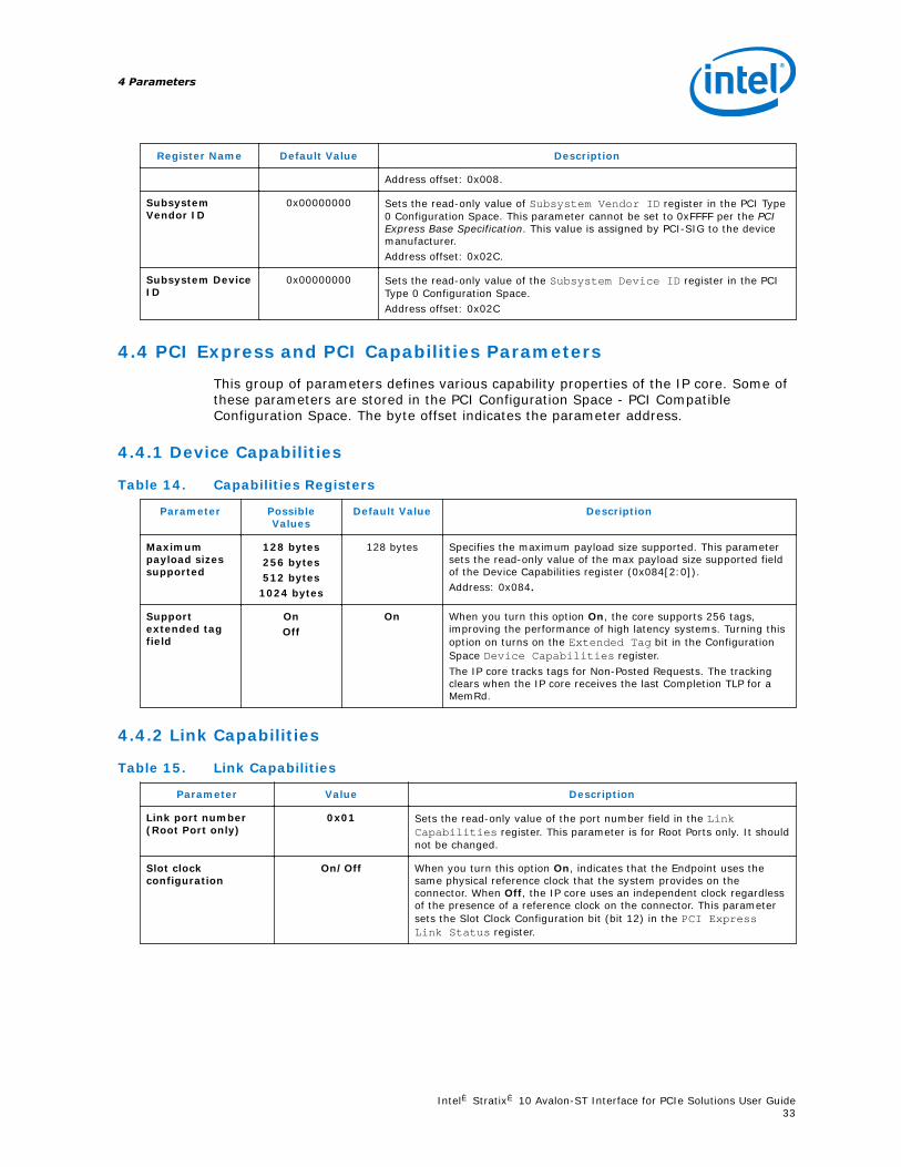
4.4 PCI Express and PCI Capabilities Parameters
This group of parameters defines various capability properties of the IP core. Some ofthese parameters are stored in the PCI Configuration Space - PCI CompatibleConfiguration Space. The byte offset indicates the parameter address.
4.4.1 Device Capabilities
Table 14. Capabilities Registers
Parameter PossibleValues
Default Value Description
Maximumpayload sizessupported
128 bytes256 bytes512 bytes
1024 bytes
128 bytes Specifies the maximum payload size supported. This parametersets the read-only value of the max payload size supported fieldof the Device Capabilities register (0x084[2:0]).Address: 0x084.
Supportextended tagfield
OnOff
On When you turn this option On, the core supports 256 tags,improving the performance of high latency systems. Turning thisoption on turns on the Extended Tag bit in the ConfigurationSpace Device Capabilities register.The IP core tracks tags for Non-Posted Requests. The trackingclears when the IP core receives the last Completion TLP for aMemRd.
4.4.2 Link Capabilities
Table 15. Link Capabilities
Parameter Value Description
Link port number(Root Port only)
0x01 Sets the read-only value of the port number field in the LinkCapabilities register. This parameter is for Root Ports only. It shouldnot be changed.
Slot clockconfiguration
On/Off When you turn this option On, indicates that the Endpoint uses thesame physical reference clock that the system provides on theconnector. When Off, the IP core uses an independent clock regardlessof the presence of a reference clock on the connector. This parametersets the Slot Clock Configuration bit (bit 12) in the PCI ExpressLink Status register.
4 Parameters
Intel® Stratix® 10 Avalon-ST Interface for PCIe Solutions User Guide33

4.4.3 MSI and MSI-X Capabilities
Table 16. MSI and MSI-X Capabilities
Parameter Value Description
MSI messagesrequested
1, 2, 4, 8, 16, 32 Specifies the number of messages the Application Layer canrequest. Sets the value of the Multiple Message Capable fieldof the Message Control register,Address: 0x050[31:16].
MSI-X Capabilities
Implement MSI-X On/Off When On, adds the MSI-X functionality.
Bit Range
Table size [15:0] System software reads this field to determine the MSI-X Table size<n>, which is encoded as <n–1>. For example, a returned value of2047 indicates a table size of 2048. This field is read-only. Legalrange is 0–2047 (216).Address offset: 0x068[26:16]
Table offset [31:0] Points to the base of the MSI-X Table. The lower 3 bits of the tableBAR indicator (BIR) are set to zero by software to form a 64-bitqword-aligned offset. This field is read-only.
Table BAR indicator [2:0] Specifies which one of a function’s BARs, located beginning at 0x10in Configuration Space, is used to map the MSI-X table into memoryspace. This field is read-only. Legal range is 0–5.
Pending bit array (PBA)offset
[31:0] Used as an offset from the address contained in one of thefunction’s Base Address registers to point to the base of the MSI-XPBA. The lower 3 bits of the PBA BIR are set to zero by software toform a 32-bit qword-aligned offset. This field is read-only. 1
Pending BAR indicator [2:0] Specifies the function Base Address registers, located beginning at0x10 in Configuration Space, that maps the MSI-X PBA into memoryspace. This field is read-only. Legal range is 0–5.
4.4.4 Slot Capabilities
Table 17. Slot Capabilities
Parameter Value Description
Use Slot register On/Off This parameter is only supported in Root Port mode. The slot capability isrequired for Root Ports if a slot is implemented on the port. Slot status isrecorded in the PCI Express Capabilities register.Defines the characteristics of the slot. You turn on this option by selectingEnable slot capability. Refer to the figure below for bit definitions.
Slot power scale 0–3 Specifies the scale used for the Slot power limit. The following coefficientsare defined:• 0 = 1.0x• 1 = 0.1x• 2 = 0.01x• 3 = 0.001x
continued...
1 Throughout this user guide, the terms word, dword and qword have the same meaning thatthey have in the PCI Express Base Specification. A word is 16 bits, a dword is 32 bits, and aqword is 64 bits.
4 Parameters
Intel® Stratix® 10 Avalon-ST Interface for PCIe Solutions User Guide34

Parameter Value Description
The default value prior to hardware and firmware initialization is b’00. Writesto this register also cause the port to send the Set_Slot_Power_LimitMessage.Refer to Section 6.9 of the PCI Express Base Specification Revision for moreinformation.
Slot power limit 0–255 In combination with the Slot power scale value, specifies the upper limit inwatts on power supplied by the slot. Refer to Section 7.8.9 of the PCI ExpressBase Specification for more information.
Slot number 0-8191 Specifies the slot number.
Figure 25. Slot Capability
31 19 18 17 16 15 14 7 6 5
Physical Slot Number
No Command Completed SupportElectromechanical Interlock Present
Slot Power Limit ScaleSlot Power Limit Value
Hot-Plug CapableHot-Plug Surprise
Power Indicator PresentAttention Indicator Present
MRL Sensor PresentPower Controller PresentAttention Button Present
04 3 2 1
4.4.5 Power Management
Table 18. Power Management Parameters
Parameter Value Description
Endpoint L0sacceptable latency
Maximum of 64 nsMaximum of 128 nsMaximum of 256 nsMaximum of 512 nsMaximum of 1 usMaximum of 2 usMaximum of 4 usNo limit
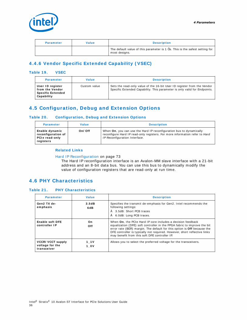
This design parameter specifies the maximum acceptable latency thatthe device can tolerate to exit the L0s state for any links between thedevice and the root complex. It sets the read-only value of theEndpoint L0s acceptable latency field of the Device CapabilitiesRegister (0x084).This Endpoint does not support the L0s or L1 states. However, in aswitched system there may be links connected to switches that haveL0s and L1 enabled. This parameter is set to allow system configurationsoftware to read the acceptable latencies for all devices in the systemand the exit latencies for each link to determine which links can enableActive State Power Management (ASPM). This setting is disabled forRoot Ports.The default value of this parameter is 64 ns. This is the safest settingfor most designs.
Endpoint L1acceptable latency
Maximum of 1 usMaximum of 2 usMaximum of 4 usMaximum of 8 usMaximum of 16 usMaximum of 32 usNo limit
This value indicates the acceptable latency that an Endpoint canwithstand in the transition from the L1 to L0 state. It is an indirectmeasure of the Endpoint’s internal buffering. It sets the read-only valueof the Endpoint L1 acceptable latency field of the DeviceCapabilities Register.This Endpoint does not support the L0s or L1 states. However, aswitched system may include links connected to switches that have L0sand L1 enabled. This parameter is set to allow system configurationsoftware to read the acceptable latencies for all devices in the systemand the exit latencies for each link to determine which links can enableActive State Power Management (ASPM). This setting is disabled forRoot Ports.
continued...
4 Parameters
Intel® Stratix® 10 Avalon-ST Interface for PCIe Solutions User Guide35
Parameter Value Description
The default value of this parameter is 1 µs. This is the safest setting formost designs.
4.4.6 Vendor Specific Extended Capability (VSEC)
Table 19. VSEC
Parameter Value Description
User ID registerfrom the VendorSpecific ExtendedCapability
Custom value Sets the read-only value of the 16-bit User ID register from the VendorSpecific Extended Capability. This parameter is only valid for Endpoints.
4.5 Configuration, Debug and Extension Options
Table 20. Configuration, Debug and Extension Options
Parameter Value Description
Enable dynamicreconfiguration ofPCIe read-onlyregisters
On/Off When On, you can use the Hard IP reconfiguration bus to dynamicallyreconfigure Hard IP read-only registers. For more information refer to HardIP Reconfiguration Interface.
Related Links
Hard IP Reconfiguration on page 73The Hard IP reconfiguration interface is an Avalon-MM slave interface with a 21-bitaddress and an 8-bit data bus. You can use this bus to dynamically modify thevalue of configuration registers that are read-only at run time.
4.6 PHY Characteristics
Table 21. PHY Characteristics
Parameter Value Description
Gen2 TX de-emphasis
3.5dB6dB
Specifies the transmit de-emphasis for Gen2. Intel recommends thefollowing settings:• 3.5dB: Short PCB traces• 6.0dB: Long PCB traces.
Enable soft DFEcontroller IP
OnOff
When On, the PCIe Hard IP core includes a decision feedbackequalization (DFE) soft controller in the FPGA fabric to improve the biterror rate (BER) margin. The default for this option is Off because theDFE controller is typically not required. However, short reflective linksmay benefit from this soft DFE controller IP.
VCCR/VCCT supplyvoltage for thetransceiver
1_1V1_0V
Allows you to select the preferred voltage for the transceivers.
4 Parameters
Intel® Stratix® 10 Avalon-ST Interface for PCIe Solutions User Guide36
4.7 Stratix 10 Example Designs
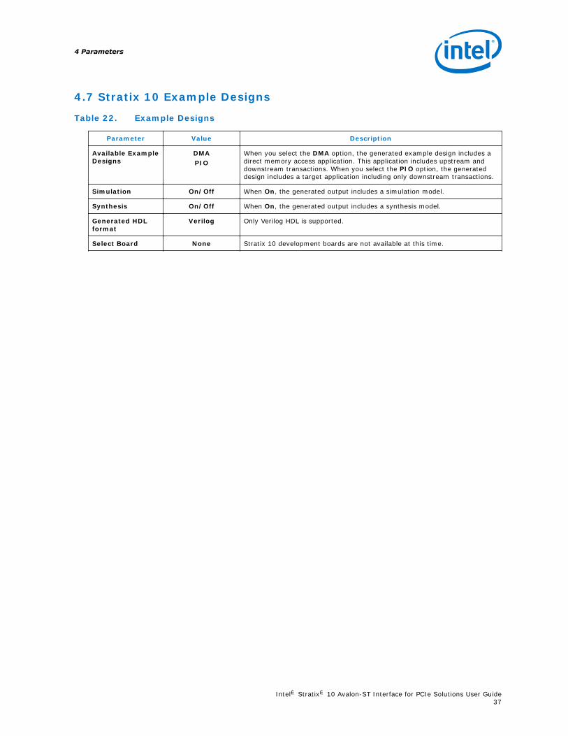
Table 22. Example Designs
Parameter Value Description
Available ExampleDesigns
DMAPIO
When you select the DMA option, the generated example design includes adirect memory access application. This application includes upstream anddownstream transactions. When you select the PIO option, the generateddesign includes a target application including only downstream transactions.
Simulation On/Off When On, the generated output includes a simulation model.
Synthesis On/Off When On, the generated output includes a synthesis model.
Generated HDLformat
Verilog Only Verilog HDL is supported.
Select Board None Stratix 10 development boards are not available at this time.
4 Parameters
Intel® Stratix® 10 Avalon-ST Interface for PCIe Solutions User Guide37

5 Designing with the IP Core
5.1 Generation
Use Qsys Pro to define and generate an Avalon-ST Stratix 10 Hard IP for PCI ExpressIP Core custom component.
Qsys Pro requires you to define a Quartus Prime project before customizing the PCIeIP core in Qsys Pro.
1. In the Quartus Prime Pro software, create a new project (File ➤ New ProjectWizard).
2. Specify the Directory, Name, and Top-Level Entity.
3. For Project Type, accept the default value, Empty project.
4. For Add Files, click Next.
5. For Family, Device & Board Settings, under Family, select Stratix 10(GX/SX) and the Target Device for your design. Refer to Stratix 10 ProductTable for information about package options.
6. Click Finish.
7. To define your Qsys Pro project, select Tools ➤ Qsys Pro.
8. For Qsys System or IP Variant, click + and specify a File name. Click Create.Click create again.
Figure 26. Qsys Pro Create New System
9. In the IP Catalog, locate and select Avalon-ST Stratix 10 Hard IP for PCIExpress.
5 Designing with the IP Core
Intel Corporation. All rights reserved. Intel, the Intel logo, Altera, Arria, Cyclone, Enpirion, MAX, Nios, Quartusand Stratix words and logos are trademarks of Intel Corporation or its subsidiaries in the U.S. and/or othercountries. Intel warrants performance of its FPGA and semiconductor products to current specifications inaccordance with Intel's standard warranty, but reserves the right to make changes to any products and servicesat any time without notice. Intel assumes no responsibility or liability arising out of the application or use of anyinformation, product, or service described herein except as expressly agreed to in writing by Intel. Intelcustomers are advised to obtain the latest version of device specifications before relying on any publishedinformation and before placing orders for products or services.*Other names and brands may be claimed as the property of others.
ISO9001:2008Registered

The parameter editor appears.
10. On the IP Settings tabs, specify the parameters for your IP variation.
Refer to the Parameters chapter for an explanations of all parameters.
11. Click Finish to exit the parameter editor.
— You can now generate a simulation testbench for your customized PCIe IP coreor continue to build your system design.
Related Links
• Parameters on page 31This chapter provides a reference for all the parameters of the Stratix 10 HardIP for PCI Express IP core.
• Creating a System with Qsys
• Stratix 10 Product Table
5.2 Simulation
After you install the Quartus Prime Pro v17.1 Stratix 10 ES Editions Software, you candownload Quartus Prime Archive Files (.qar) from <install_dir>ip\altera\altera_pcie\altera_pcie_s10_ed\example_design\s10. This directoryincludes example designs for the following Endpoint configurations:
• Gen1, Gen2, and Gen3
• x1, x2, x4, x8, and x16
• Avalon-ST, Avalon-MM, and Avalon-MM with DMA
The simulation testbench supports only the Verilog HDL and the following simulators:
• Mentor: ModelSim SE
• Synopsys: VCS
If you choose to simulate an example design from the Quartus Prime Pro installation,the testbench includes the following components:
• An Endpoint (DUT)
• A Root Port BFM
• Memory (MEM)
The examples provided with the Quartus Prime Pro – Stratix 10 Edition 17.1 InterimRelease software installation are static. Consequently, you cannot modify theparameters and regenerate the example design.
Note: The Intel testbench and Root Port BFM provide a simple method to do basic testing ofthe Application Layer logic that interfaces to the variation. This BFM allows you tocreate and run simple task stimuli with configurable parameters to exercise basicfunctionality of the example design. The testbench and Root Port BFM are not intendedto be a substitute for a full verification environment. Corner cases and certain trafficprofile stimuli are not covered. To ensure the best verification coverage possible, Intelsuggests strongly that you obtain commercially available PCI Express verification IPand tools, or do your own extensive hardware testing or both.
5 Designing with the IP Core
Intel® Stratix® 10 Avalon-ST Interface for PCIe Solutions User Guide39

Refer to the Example Design for Avalon-ST Stratix 10 Hard IP for PCI Express chapterto create a simple custom example design using the parameters that you specify.
Related Links
Generating the Design
5.2.1 Selecting Serial or PIPE Simulation
The parameter serial_sim_hwtcl in <working_dir>/<variant>_example_design/pcie_example_design_tb/pcie_example_design_tb/altera_pcie_<dev>_tbed_<ver>/sim/altpcied_<dev>_hwtcl.sv determines the simulation mode. When 1'b1, thesimulation is serial. When 1'b0, the simulation runs in the 32-bit parallel PIPE mode.
5.2.2 Reducing Counter Values for Simulation
You can save simulation time by reducing the value of counters whose default valuesare set appropriately for hardware. The test_in[0] signal controls the values.Setting test_in[0]= 1'b, reduces counter values for simulation. (By default, thegenerated simulation testbench does set test_in[0]= 1'b.)
5.3 Files Generated for Intel FPGA IP Cores and Qsys Pro Systems
The Quartus Prime Pro Edition software generates the following output file structurefor IP cores and Qsys Pro systems. The Quartus Prime Pro Edition softwareautomatically adds the .ip files and the generated .qsys files when you open yourQuartus Prime Pro project.
5 Designing with the IP Core
Intel® Stratix® 10 Avalon-ST Interface for PCIe Solutions User Guide40

Figure 27. Files generated for IP cores and Qsys Pro Systems
<Project Directory>
<your_ip>_inst.v or .vhd - Lists file for IP core synthesis
<your_ip>.qip - Lists files for IP core synthesis
<your_ip>.debuginfo - Post-generation debug data
<your_ip>_generation.rpt - IP generation report
<your_ip>.bsf - Block symbol schematic file
<your_ip>.ppf - XML I/O pin information file
<your_ip>.html - Memory map data
<your_ip>.cmp - VHDL component declaration
<your_ip>.sip - NativeLink simulation integration file
<your_ip>.spd - Combines individual simulation startup scripts
<your_system>.qsys - System File<your_subsystem>.qsys - Subsystem File
<your_system_directory>
<your_subsystem_directory>
<your_ip>.ipxact - IP XACT File
sim - IP simulation files
<simulator vendor> - Simulator setup scripts
<your_ip>.v or vhd - Top-level simulation file
synth - IP synthesis files
<your_ip>.v or .vhd - Top-level IP synthesis file
ip - IP files
<your_system> - - Your system directory
<your_system>.ip - Parameter file for system IP component
<your_subsystem> - Your Subsystem directory
<your_subsystem>.ip - Parameter file for subsystem IP component
<your_ip>_bb.v - Verilog HDL black box EDA synthesis file
<your_ip>.qgsimc - Simulation caching file
<your_ip>.qgsynthc - Synthesis caching file
Table 23. IP Core and Qsys Simulation Files
File Name Description
<my_system>.qsys The Qsys Pro system.
<my_subsystem>.qsys The Qsys Pro subsystem.
ip/ Contains the parameter files for the IP components in the system andsubsystem(s).
continued...
5 Designing with the IP Core
Intel® Stratix® 10 Avalon-ST Interface for PCIe Solutions User Guide41
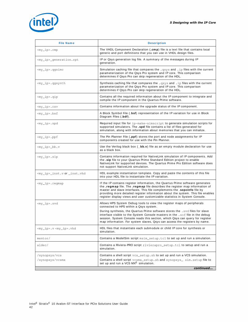
File Name Description
<my_ip>.cmp The VHDL Component Declaration (.cmp) file is a text file that contains localgeneric and port definitions that you can use in VHDL design files.
<my_ip>_generation.rpt IP or Qsys generation log file. A summary of the messages during IPgeneration.
<my_ip>.qgsimc Simulation caching file that compares the .qsys and .ip files with the currentparameterization of the Qsys Pro system and IP core. This comparisondetermines if Qsys Pro can skip regeneration of the HDL.
<my_ip>.qgsynth Synthesis caching file that compares the .qsys and .ip files with the currentparameterization of the Qsys Pro system and IP core. This comparisondetermines if Qsys Pro can skip regeneration of the HDL.
<my_ip>.qip Contains all the required information about the IP component to integrate andcompile the IP component in the Quartus Prime software.
<my_ip>.csv Contains information about the upgrade status of the IP component.
<my_ip>.bsf A Block Symbol File (.bsf) representation of the IP variation for use in BlockDiagram Files (.bdf).
<my_ip>.spd Required input file for ip-make-simscript to generate simulation scripts forsupported simulators. The .spd file contains a list of files generated forsimulation, along with information about memories that you can initialize.
<my_ip>.ppf The Pin Planner File (.ppf) stores the port and node assignments for IPcomponents created for use with the Pin Planner.
<my_ip>_bb.v Use the Verilog black box (_bb.v) file as an empty module declaration for useas a black box.
<my_ip>.sip Contains information required for NativeLink simulation of IP components. Addthe .sip file to your Quartus Prime Standard Edition project to enableNativeLink for supported devices. The Quartus Prime Pro Edition software doesnot support NativeLink simulation.
<my_ip>_inst.v or _inst.vhd HDL example instantiation template. Copy and paste the contents of this fileinto your HDL file to instantiate the IP variation.
<my_ip>.regmap If the IP contains register information, the Quartus Prime software generatesthe .regmap file. The .regmap file describes the register map information ofmaster and slave interfaces. This file complements the .sopcinfo file byproviding more detailed register information about the system. This file enablesregister display views and user customizable statistics in System Console.
<my_ip>.svd Allows HPS System Debug tools to view the register maps of peripheralsconnected to HPS within a Qsys system.During synthesis, the Quartus Prime software stores the .svd files for slaveinterface visible to the System Console masters in the .sof file in the debugsession. System Console reads this section, which Qsys can query for registermap information. For system slaves, Qsys can access the registers by name.
<my_ip>.v <my_ip>.vhd HDL files that instantiate each submodule or child IP core for synthesis orsimulation.
mentor/ Contains a ModelSim script msim_setup.tcl to set up and run a simulation.
aldec/ Contains a Riviera-PRO script rivierapro_setup.tcl to setup and run asimulation.
/synopsys/vcs
/synopsys/vcsmx
Contains a shell script vcs_setup.sh to set up and run a VCS simulation.Contains a shell script vcsmx_setup.sh and synopsys_ sim.setup file toset up and run a VCS MX® simulation.
continued...
5 Designing with the IP Core
Intel® Stratix® 10 Avalon-ST Interface for PCIe Solutions User Guide42
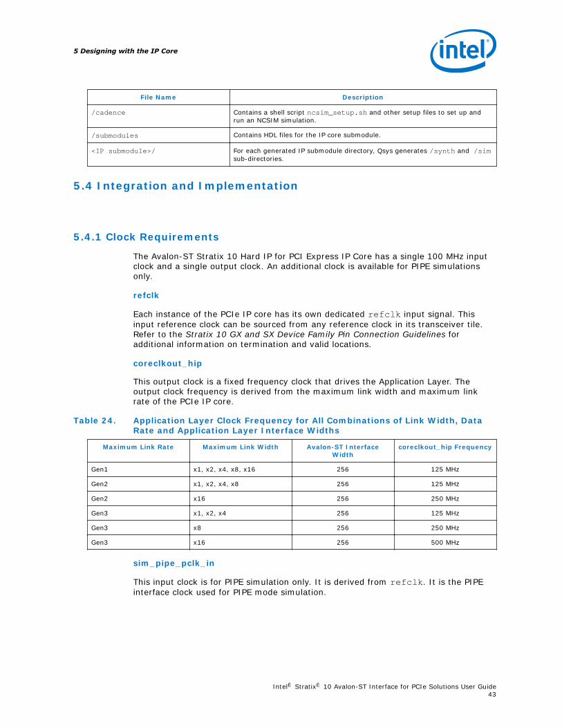
File Name Description
/cadence Contains a shell script ncsim_setup.sh and other setup files to set up andrun an NCSIM simulation.
/submodules Contains HDL files for the IP core submodule.
<IP submodule>/ For each generated IP submodule directory, Qsys generates /synth and /simsub-directories.
5.4 Integration and Implementation
5.4.1 Clock Requirements
The Avalon-ST Stratix 10 Hard IP for PCI Express IP Core has a single 100 MHz inputclock and a single output clock. An additional clock is available for PIPE simulationsonly.
refclk
Each instance of the PCIe IP core has its own dedicated refclk input signal. Thisinput reference clock can be sourced from any reference clock in its transceiver tile.Refer to the Stratix 10 GX and SX Device Family Pin Connection Guidelines foradditional information on termination and valid locations.
coreclkout_hip
This output clock is a fixed frequency clock that drives the Application Layer. Theoutput clock frequency is derived from the maximum link width and maximum linkrate of the PCIe IP core.
Table 24. Application Layer Clock Frequency for All Combinations of Link Width, DataRate and Application Layer Interface Widths
Maximum Link Rate Maximum Link Width Avalon-ST InterfaceWidth
coreclkout_hip Frequency
Gen1 x1, x2, x4, x8, x16 256 125 MHz
Gen2 x1, x2, x4, x8 256 125 MHz
Gen2 x16 256 250 MHz
Gen3 x1, x2, x4 256 125 MHz
Gen3 x8 256 250 MHz
Gen3 x16 256 500 MHz
sim_pipe_pclk_in
This input clock is for PIPE simulation only. It is derived from refclk. It is the PIPEinterface clock used for PIPE mode simulation.
5 Designing with the IP Core
Intel® Stratix® 10 Avalon-ST Interface for PCIe Solutions User Guide43

5.4.2 Reset Requirements
The Avalon-ST Stratix 10 Hard IP for PCI Express IP Core has two, asynchronous,active low reset inputs, npor and pin_perst. Both reset the Transaction, Data Linkand Physical Layers.
npor
The Application Layer drives the npor reset input to the PCIe IP core. If you choose todesign an Application Layer does not drive npor, you must tie this output to 1'b1. Thenpor signal resets all registers and state machines to their initial values.
pin_perst
This is the PCI Express Fundamental Reset signal. Asserting this signal returns allregisters and state machines to their initialization values. Each instance of the PCIe IPcore has its own dedicated pin_perst pin. You must connect the pin_perst of eachhard IP instance to the corresponding nPERST pin of the device. These pins have thefollowing location.
• NPERSTL0 : Bottom Left PCIe IP core and Configuration via Protocol (CvP)
• NPERSTL1: Middle Left PCIe PCIe IP core (When available)
• NPERSTL2: Top Left PCIe IP core (When available)
• NPERSTR0: Bottom Right PCIe IP core (When available)
• NPERSTR1: Middle Right PCIe IP core (When available)
• NPERSTR2: Top Right PCIe IP core (When available)
For maximum compatibility, always use the bottom PCIe IP core on the left side of thedevice first. This is the only location that supports CvP using the PCIe link.
Note: CvP is not available in the Quartus Prime Pro – Stratix 10 Edition 17.1 Interim Release
reset_status
When asserted, this signal indicates that the PCIe IP core is in reset. Thereset_status signal is synchronous to coreclkout_hip. It is active high.
clr_st
This signal has the same functionality as reset_status. It is provided for backwardscompatibility with Arria 10 devices. It is active high.
5.5 Required Supporting IP Cores
Stratix 10 Hard IP for PCI Express IP core designs always include the Hard ResetController and TX PLL IP cores. System generation automatically adds thesecomponents to the generated design.
5 Designing with the IP Core
Intel® Stratix® 10 Avalon-ST Interface for PCIe Solutions User Guide44

5.5.1 Hard Reset Controller
The Hard Reset Controller generates the reset for the PCIe IP core logic, transceivers,and Application Layer. To meet 100 ms PCIe configuration time, the Hard ResetController interfaces with the SDM. This allows the PCIe Hard IP to be configured firstso that PCIe link training occurs when the FPGA fabric is still being configured.
5.5.2 TX PLL
For Gen1 or Gen2, the PCIe IP core uses the fractional PLL ( fPLL) for the TX PLL. ForGen3, the PCIe Hard IP core uses the fPLL when operating at the Gen1 or Gen2 datarate. It uses the advanced transmit (ATX) PLL when operating at the Gen3 data rate.
Note: The ATX PLL is sometimes called the LC PLL, where LC refers to inductor/capacitor.
5.6 Channel Layout and PLL Usage
The following figures show the channel layout and connection between the Hard ResetController (HRC) and PLLs and for Gen1, Gen2 and Gen3 x1, x2, x4, x8 and x16variants of the Stratix 10 Hard IP for PCI Express IP core. The channel layout is thesame for the Avalon-ST and Avalon-MM interfaces to the Application Layer.
Note: All of the PCIe hard IP instances in Stratix 10 devices are Gen3 x16. The Hard ResetController drives all 16 channels. However, channels 8-15 are available for otherprotocols when fewer than 16 channels are used. Refer to Channel Availability formore information.
Figure 28. Gen1 and Gen2 x1
PMA Channel 5PMA Channel 4PMA Channel 3PMA Channel 2PMA Channel 1PMA Channel 0
PCS Channel 5PCS Channel 4PCS Channel 3PCS Channel 2PCS Channel 1PCS Channel 0
fPLL1
fPLL0
ATXPLL0
ATXPLL1
PMA Channel 5PMA Channel 4PMA Channel 3PMA Channel 2PMA Channel 1PMA Channel 0
PCS Channel 5PCS Channel 4PCS Channel 3PCS Channel 2PCS Channel 1PCS Channel 0
fPLL1
fPLL0
ATXPLL0
ATXPLL1
PMA Channel 5PMA Channel 4PMA Channel 3PMA Channel 2PMA Channel 1PMA Channel 0
PCS Channel 5PCS Channel 4PCS Channel 3PCS Channel 2PCS Channel 1PCS Channel 0
fPLL1
fPLL0
ATXPLL0
ATXPLL1
PMA Channel 5PMA Channel 4PMA Channel 3PMA Channel 2PMA Channel 1PMA Channel 0
PCS Channel 5PCS Channel 4PCS Channel 3PCS Channel 2PCS Channel 1PCS Channel 0
fPLL1
fPLL0
ATXPLL0
ATXPLL1
Ch 15Ch 14Ch 13Ch 12Ch 11Ch 10Ch 9Ch 8Ch 7Ch 6Ch 5Ch 4Ch 3Ch 2Ch 1Ch 0
PCIe Hard IP
HRCconnects to
fPLL0
5 Designing with the IP Core
Intel® Stratix® 10 Avalon-ST Interface for PCIe Solutions User Guide45

Figure 29. Gen1 and Gen2 x2
PMA Channel 5PMA Channel 4PMA Channel 3PMA Channel 2PMA Channel 1PMA Channel 0
PCS Channel 5PCS Channel 4PCS Channel 3PCS Channel 2PCS Channel 1PCS Channel 0
fPLL1
fPLL0
ATXPLL0
ATXPLL1
PMA Channel 5PMA Channel 4PMA Channel 3PMA Channel 2PMA Channel 1PMA Channel 0
PCS Channel 5PCS Channel 4PCS Channel 3PCS Channel 2PCS Channel 1PCS Channel 0
fPLL1
fPLL0
ATXPLL0
ATXPLL1
PMA Channel 5PMA Channel 4PMA Channel 3PMA Channel 2PMA Channel 1PMA Channel 0
PCS Channel 5PCS Channel 4PCS Channel 3PCS Channel 2PCS Channel 1PCS Channel 0
fPLL1
fPLL0
ATXPLL0
ATXPLL1
PMA Channel 5PMA Channel 4PMA Channel 3PMA Channel 2PMA Channel 1PMA Channel 0
PCS Channel 5PCS Channel 4PCS Channel 3PCS Channel 2PCS Channel 1PCS Channel 0
fPLL1
fPLL0
ATXPLL0
ATXPLL1
Ch 15Ch 14Ch 13Ch 12Ch 11Ch 10Ch 9Ch 8Ch 7Ch 6Ch 5Ch 4Ch 3Ch 2Ch 1Ch 0
PCIe Hard IP
HRCconnects to
fPLL0
Figure 30. Gen1 and Gen2 x4
PMA Channel 5PMA Channel 4PMA Channel 3PMA Channel 2PMA Channel 1PMA Channel 0
PCS Channel 5PCS Channel 4PCS Channel 3PCS Channel 2PCS Channel 1PCS Channel 0
fPLL1
fPLL0
ATXPLL0
ATXPLL1
PMA Channel 5PMA Channel 4PMA Channel 3PMA Channel 2PMA Channel 1PMA Channel 0
PCS Channel 5PCS Channel 4PCS Channel 3PCS Channel 2PCS Channel 1PCS Channel 0
fPLL1
fPLL0
ATXPLL0
ATXPLL1
PMA Channel 5PMA Channel 4PMA Channel 3PMA Channel 2PMA Channel 1PMA Channel 0
PCS Channel 5PCS Channel 4PCS Channel 3PCS Channel 2PCS Channel 1PCS Channel 0
fPLL1
fPLL0
ATXPLL0
ATXPLL1
PMA Channel 5PMA Channel 4PMA Channel 3PMA Channel 2PMA Channel 1PMA Channel 0
PCS Channel 5PCS Channel 4PCS Channel 3PCS Channel 2PCS Channel 1PCS Channel 0
fPLL1
fPLL0
ATXPLL0
ATXPLL1
Ch 15Ch 14Ch 13Ch 12Ch 11Ch 10Ch 9Ch 8Ch 7Ch 6Ch 5Ch 4Ch 3Ch 2Ch 1Ch 0
PCIe Hard IP
HRCconnects to
fPLL0
5 Designing with the IP Core
Intel® Stratix® 10 Avalon-ST Interface for PCIe Solutions User Guide46

Figure 31. Gen1 and Gen2 x8
PMA Channel 5PMA Channel 4PMA Channel 3PMA Channel 2PMA Channel 1PMA Channel 0
PCS Channel 5PCS Channel 4PCS Channel 3PCS Channel 2PCS Channel 1PCS Channel 0
fPLL1
fPLL0
ATXPLL0
ATXPLL1
PMA Channel 5PMA Channel 4PMA Channel 3PMA Channel 2PMA Channel 1PMA Channel 0
PCS Channel 5PCS Channel 4PCS Channel 3PCS Channel 2PCS Channel 1PCS Channel 0
fPLL1
fPLL0
ATXPLL0
ATXPLL1
PMA Channel 5PMA Channel 4PMA Channel 3PMA Channel 2PMA Channel 1PMA Channel 0
PCS Channel 5PCS Channel 4PCS Channel 3PCS Channel 2PCS Channel 1PCS Channel 0
fPLL1
fPLL0
ATXPLL0
ATXPLL1
PMA Channel 5PMA Channel 4PMA Channel 3PMA Channel 2PMA Channel 1PMA Channel 0
PCS Channel 5PCS Channel 4PCS Channel 3PCS Channel 2PCS Channel 1PCS Channel 0
fPLL1
fPLL0
ATXPLL0
ATXPLL1
Ch 15Ch 14Ch 13Ch 12Ch 11Ch 10Ch 9Ch 8Ch 7Ch 6Ch 5Ch 4Ch 3Ch 2Ch 1Ch 0
PCIe Hard IP
HRCconnects to
fPLL0
Figure 32. Gen1 and Gen2 x16
PMA Channel 5PMA Channel 4PMA Channel 3PMA Channel 2PMA Channel 1PMA Channel 0
PCS Channel 5PCS Channel 4PCS Channel 3PCS Channel 2PCS Channel 1PCS Channel 0
fPLL1
fPLL0
ATXPLL0
ATXPLL1
PMA Channel 5PMA Channel 4PMA Channel 3PMA Channel 2PMA Channel 1PMA Channel 0
PCS Channel 5PCS Channel 4PCS Channel 3PCS Channel 2PCS Channel 1PCS Channel 0
fPLL1
fPLL0
ATXPLL0
ATXPLL1
PMA Channel 5PMA Channel 4PMA Channel 3PMA Channel 2PMA Channel 1PMA Channel 0
PCS Channel 5PCS Channel 4PCS Channel 3PCS Channel 2PCS Channel 1PCS Channel 0
fPLL1
fPLL0
ATXPLL0
ATXPLL1
PMA Channel 5PMA Channel 4PMA Channel 3PMA Channel 2PMA Channel 1PMA Channel 0
PCS Channel 5PCS Channel 4PCS Channel 3PCS Channel 2PCS Channel 1PCS Channel 0
fPLL1
fPLL0
ATXPLL0
ATXPLL1
Ch 15Ch 14Ch 13Ch 12Ch 11Ch 10Ch 9Ch 8Ch 7Ch 6Ch 5Ch 4Ch 3Ch 2Ch 1Ch 0
PCIe Hard IP
HRCconnects to
fPLL0 middleXCVR bank
5 Designing with the IP Core
Intel® Stratix® 10 Avalon-ST Interface for PCIe Solutions User Guide47

Figure 33. Gen3 x1
PMA Channel 5PMA Channel 4PMA Channel 3PMA Channel 2PMA Channel 1PMA Channel 0
PCS Channel 5PCS Channel 4PCS Channel 3PCS Channel 2PCS Channel 1PCS Channel 0
fPLL1
fPLL0
ATXPLL0
ATXPLL1
PMA Channel 5PMA Channel 4PMA Channel 3PMA Channel 2PMA Channel 1PMA Channel 0
PCS Channel 5PCS Channel 4PCS Channel 3PCS Channel 2PCS Channel 1PCS Channel 0
fPLL1
fPLL0
ATXPLL0
ATXPLL1
PMA Channel 5PMA Channel 4PMA Channel 3PMA Channel 2PMA Channel 1PMA Channel 0
PCS Channel 5PCS Channel 4PCS Channel 3PCS Channel 2PCS Channel 1PCS Channel 0
fPLL1
fPLL0ATXPLL0(Gen3)
ATXPLL1
PMA Channel 5PMA Channel 4PMA Channel 3PMA Channel 2PMA Channel 1PMA Channel 0
PCS Channel 5PCS Channel 4PCS Channel 3PCS Channel 2PCS Channel 1PCS Channel 0
fPLL1
fPLL0
ATXPLL0
ATXPLL1
Ch 15Ch 14Ch 13Ch 12Ch 11Ch 10Ch 9Ch 8Ch 7Ch 6Ch 5Ch 4Ch 3Ch 2Ch 1Ch 0
PCIe Hard IP
HRCconnects to
fPLL0 &ATXPLL0
Figure 34. Gen3 x2
PMA Channel 5PMA Channel 4PMA Channel 3PMA Channel 2PMA Channel 1PMA Channel 0
PCS Channel 5PCS Channel 4PCS Channel 3PCS Channel 2PCS Channel 1PCS Channel 0
fPLL1
fPLL0
ATXPLL0
ATXPLL1
PMA Channel 5PMA Channel 4PMA Channel 3PMA Channel 2PMA Channel 1PMA Channel 0
PCS Channel 5PCS Channel 4PCS Channel 3PCS Channel 2PCS Channel 1PCS Channel 0
fPLL1
fPLL0
ATXPLL0
ATXPLL1
PMA Channel 5PMA Channel 4PMA Channel 3PMA Channel 2PMA Channel 1PMA Channel 0
PCS Channel 5PCS Channel 4PCS Channel 3PCS Channel 2PCS Channel 1PCS Channel 0
fPLL1
fPLL0ATXPLL0(Gen3)
ATXPLL1
PMA Channel 5PMA Channel 4PMA Channel 3PMA Channel 2PMA Channel 1PMA Channel 0
PCS Channel 5PCS Channel 4PCS Channel 3PCS Channel 2PCS Channel 1PCS Channel 0
fPLL1
fPLL0
ATXPLL0
ATXPLL1
Ch 15Ch 14Ch 13Ch 12Ch 11Ch 10Ch 9Ch 8Ch 7Ch 6Ch 5Ch 4Ch 3Ch 2Ch 1Ch 0
PCIe Hard IP
HRCconnects to
fPLL0 &ATXPLL0
5 Designing with the IP Core
Intel® Stratix® 10 Avalon-ST Interface for PCIe Solutions User Guide48

Figure 35. Gen3 x4
PMA Channel 5PMA Channel 4PMA Channel 3PMA Channel 2PMA Channel 1PMA Channel 0
PCS Channel 5PCS Channel 4PCS Channel 3PCS Channel 2PCS Channel 1PCS Channel 0
fPLL1
fPLL0
ATXPLL0
ATXPLL1
PMA Channel 5PMA Channel 4PMA Channel 3PMA Channel 2PMA Channel 1PMA Channel 0
PCS Channel 5PCS Channel 4PCS Channel 3PCS Channel 2PCS Channel 1PCS Channel 0
fPLL1
fPLL0
ATXPLL0
ATXPLL1
PMA Channel 5PMA Channel 4PMA Channel 3PMA Channel 2PMA Channel 1PMA Channel 0
PCS Channel 5PCS Channel 4PCS Channel 3PCS Channel 2PCS Channel 1PCS Channel 0
fPLL1
fPLL0ATXPLL0(Gen3)
ATXPLL1
PMA Channel 5PMA Channel 4PMA Channel 3PMA Channel 2PMA Channel 1PMA Channel 0
PCS Channel 5PCS Channel 4PCS Channel 3PCS Channel 2PCS Channel 1PCS Channel 0
fPLL1
fPLL0
ATXPLL0
ATXPLL1
Ch 15Ch 14Ch 13Ch 12Ch 11Ch 10Ch 9Ch 8Ch 7Ch 6Ch 5Ch 4Ch 3Ch 2Ch 1Ch 0
PCIe Hard IP
HRCconnects to
fPLL0 &ATXPLL0
Figure 36. Gen3 x8
PMA Channel 5PMA Channel 4PMA Channel 3PMA Channel 2PMA Channel 1PMA Channel 0
PCS Channel 5PCS Channel 4PCS Channel 3PCS Channel 2PCS Channel 1PCS Channel 0
fPLL1
fPLL0
ATXPLL0
ATXPLL1
PMA Channel 5PMA Channel 4PMA Channel 3PMA Channel 2PMA Channel 1PMA Channel 0
PCS Channel 5PCS Channel 4PCS Channel 3PCS Channel 2PCS Channel 1PCS Channel 0
fPLL1
fPLL0
ATXPLL0
ATXPLL1
PMA Channel 5PMA Channel 4PMA Channel 3PMA Channel 2PMA Channel 1PMA Channel 0
PCS Channel 5PCS Channel 4PCS Channel 3PCS Channel 2PCS Channel 1PCS Channel 0
fPLL1
fPLL0ATXPLL0(Gen3)
ATXPLL1
PMA Channel 5PMA Channel 4PMA Channel 3PMA Channel 2PMA Channel 1PMA Channel 0
PCS Channel 5PCS Channel 4PCS Channel 3PCS Channel 2PCS Channel 1PCS Channel 0
fPLL1
fPLL0
ATXPLL0
ATXPLL1
Ch 15Ch 14Ch 13Ch 12Ch 11Ch 10Ch 9Ch 8Ch 7Ch 6Ch 5Ch 4Ch 3Ch 2Ch 1Ch 0
PCIe Hard IP
HRCconnects to
fPLL0 &ATXPLL0
5 Designing with the IP Core
Intel® Stratix® 10 Avalon-ST Interface for PCIe Solutions User Guide49

Figure 37. Gen3 x16
PMA Channel 5PMA Channel 4PMA Channel 3PMA Channel 2PMA Channel 1PMA Channel 0
PCS Channel 5PCS Channel 4PCS Channel 3PCS Channel 2PCS Channel 1PCS Channel 0
fPLL1
fPLL0
ATXPLL0
ATXPLL1
PMA Channel 5PMA Channel 4PMA Channel 3PMA Channel 2PMA Channel 1PMA Channel 0
PCS Channel 5PCS Channel 4PCS Channel 3PCS Channel 2PCS Channel 1PCS Channel 0
fPLL1
fPLL0
ATXPLL0
ATXPLL1
PMA Channel 5PMA Channel 4PMA Channel 3PMA Channel 2PMA Channel 1PMA Channel 0
PCS Channel 5PCS Channel 4PCS Channel 3PCS Channel 2PCS Channel 1PCS Channel 0
fPLL1
fPLL0ATXPLL0(Gen3)
ATXPLL1
PMA Channel 5PMA Channel 4PMA Channel 3PMA Channel 2PMA Channel 1PMA Channel 0
PCS Channel 5PCS Channel 4PCS Channel 3PCS Channel 2PCS Channel 1PCS Channel 0
fPLL1
fPLL0
ATXPLL0
ATXPLL1
Ch 15Ch 14Ch 13Ch 12Ch 11Ch 10Ch 9Ch 8Ch 7Ch 6Ch 5Ch 4Ch 3Ch 2Ch 1Ch 0
PCIe Hard IP
HRCconnects to
fPLL0 &ATXPLL1middle
XCVR bank
Related Links
Channel Availability on page 15
5.7 Compiling the Full Design and Programming the FPGA
You can use the Start Compilation command on the Processing menu in the QuartusPrime software to compile your design. After successfully compiling your design,program the targeted Intel device with the Programmer and verify the design inhardware.
Related Links
Programming Intel Devices
5 Designing with the IP Core
Intel® Stratix® 10 Avalon-ST Interface for PCIe Solutions User Guide50

6 Block DescriptionsThe Stratix 10 Hard IP for PCI Express implements the complete PCI Express protocolstack as defined in the PCI Express Base Specification. The protocol stack includes thefollowing layers:
• Transaction Layer—The Transaction Layer contains the Configuration Space, whichmanages communication with the Application Layer, the RX and TX channels, theRX buffer, and flow control credits.
• Data Link Layer—The Data Link Layer, located between the Physical Layer and theTransaction Layer, manages packet transmission and maintains data integrity atthe link level. Specifically, the Data Link Layer performs the following tasks:
— Manages transmission and reception of Data Link Layer Packets (DLLPs)
— Generates all transmission link cyclical redundancy code (LCRC) values andchecks all LCRCs during reception
— Manages the retry buffer and retry mechanism according to received ACK/NAKData Link Layer packets
— Initializes the flow control mechanism for DLLPs and routes flow control creditsto and from the Transaction Layer
• Physical Layer—The Physical Layer initializes the speed, lane numbering, and lanewidth of the PCI Express link according to packets received from the link anddirectives received from higher layers. The following figure provides a high-levelblock diagram.
Figure 38. Stratix 10 Hard IP for PCI Express Using the Avalon-ST Interface
Channels to FPGAAvalon-ST Interface
MappingPLL
Embe
dded
Mult
i-die
Inte
rconn
ect B
ridge
Stratix 10 Avalon-ST Hard IP for PCIe IP Core (altpcie_s10_hip_pipen1b.v)
PCIe Variant with Avalon-ST Interface
H-Tile or L-Tile
PCIe Link
Gen3x16 PCI Express IP Core
Data Link LayerTransaction Layer
Avalon-ST TX
Avalon-ST RX
Hdr & Data Credits
MSI/MSI-X
Clocks
ResetsPCS and PMA
Each channel of the Physical Layer is paired with an Embedded Multi-die InterconnectBridge (EMIB) module. The FPGA fabric interfaces to the PCI Express IP core throughthe EMIB. The TX and RX interfaces each connect to four EMIB modules.
6 Block Descriptions
Intel Corporation. All rights reserved. Intel, the Intel logo, Altera, Arria, Cyclone, Enpirion, MAX, Nios, Quartusand Stratix words and logos are trademarks of Intel Corporation or its subsidiaries in the U.S. and/or othercountries. Intel warrants performance of its FPGA and semiconductor products to current specifications inaccordance with Intel's standard warranty, but reserves the right to make changes to any products and servicesat any time without notice. Intel assumes no responsibility or liability arising out of the application or use of anyinformation, product, or service described herein except as expressly agreed to in writing by Intel. Intelcustomers are advised to obtain the latest version of device specifications before relying on any publishedinformation and before placing orders for products or services.*Other names and brands may be claimed as the property of others.
ISO9001:2008Registered
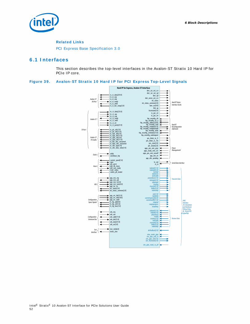
Related Links
PCI Express Base Specification 3.0
6.1 Interfaces
This section describes the top-level interfaces in the Avalon-ST Stratix 10 Hard IP forPCIe IP core.
Figure 39. Avalon-ST Stratix 10 Hard IP for PCI Express Top-Level Signals
rx_st_data[255:0] rx_st_soprx_st_eoprx_st_readyrx_st_valid rx_st_bar_range[2:0]
Hard IP for Express, Avalon-ST Interface
tx_st_data[255:0] tx_st_soptx_st_eoptx_st_readytx_st_validtx_st_errtx_st_parity[31:0]
TX Port
PowerManagementt
tx_outrx_in Serial Data Interface
Avalon-STRX Port
Avalon-ST
Clocks refclkcoreclkout_hip
int_status[3:0]int_status_common[2:0]
MSI
app_msi_reqapp_msi_ackapp_msi_tc[2:0]app_msi_num[4:0]app_int_sts
tx_ph_cdts[7:0]tx_pd_cdts[11:0]tx_nph_cdts[7:0]tx_npd_cdts[11:0]tx_cplh_cdts[7:0]tx_cpld_cdts[11:0]tx_hdr_cdts_consumedtx_data_cdts_consumedtx_cdts_type[1:0]tx_cdts_data_value[1:0]
Avalon-STTX Credits
npor
reset_status
pin_perst
serdes_pll_locked
pld_core_readypld_clk_inuse
current_speed[1:0]
Reset
derr_cor_ext_rcvderr_cor_ext_rpl
derr_rplderr_uncor_ext_rcv
int_statusint_status_common[2:0]
lane_act[4:0]link_up
ltssmstate[5:0]rx_par_errtx_par_err
Hard IP StatusInterface Clocks
tl_cfg_add[4:0]tl_cfg_ctl[31:0]tl_cfg_func[1:0]
app_err_hdr[31:0]app_err_info[10:0]
ConfigurationSpace Signals
app_err_valid
txdata0[31:0]txdatak0[3:0]
rxdata0[31:0]rxdatak[3:0]
txdetectrxtxelectidle
txcompl
rxpolarity
powerdown[1:0]txmargin[2:0]
txswing
rxvalidphystatus0
rxelecidlerxstatus[2:0]
simu_mode_pipe
sim_pipe_rate[1:0]sim_pipe_pclk_in
sim_ltssmstate[5:0]
sim_pipe_mask_tx_pll
txdeemph
txblkst[3:0]txdataskip
Transmit Data
Receive Data
PIPE Interface for Simulation and HardwareDebug Usingdl_ltssm[4:0]
in SignalTap
rxdataskiprxblkst[3:0]
txsynchd[1:0]
currentcoeff0[17:0]currentrxpreset0[2:0]
rxsynchd[3:0]
rate[1:0]
rxeqevalrxeqinprogress
invalidreq
dirfeedback[5:0]
Hard IPReconfiguration(Optional)
hip_reconfig_clkhip_reconfig_rst_n
hip_reconfig_address[20:0]hip_reconfig_read
hip_reconfig_readdata[7:0]
hip_reconfig_writehip_reconfig_writedata[15:0]
hip_reconfig_readdatavalid
hip_reconfig_waitrequest
pm_linkst_in_l1pm_linkst_in_10s
pm_state[2:0]pm_dstate[2:0]
apps_pm_xmt_pmeapps_ready_entr_l23
apps_pm_xmt_turnoffapp_init_rst
app_xfer_pending
Configuration Extension Bus
ceb_reqceb_ackceb_addr[11:0]ceb_din[31:0]ceb_dout[31:0]ceb_wr[3:0]
TestInterface
test_int[66:0]testin_zero
6 Block Descriptions
Intel® Stratix® 10 Avalon-ST Interface for PCIe Solutions User Guide52

6.1.1 TLP Header and Data Alignment for the Avalon-ST RX and TXInterfaces
The TLP header and data is packed on the TX and RX interfaces.
The ordering of bytes in the header and data portions of packets is different. The firstbyte of the header dword is located in the most significant byte of the dword. The firstbyte of the data dword is located in the least significant byte of the dword on the databus. In the figure H0 to H3 are header dwords. D0 to D9 are data dwords.
Figure 40. Three and Four DWord Header and Data on the TX and RX Interfaces
Byte 3Byte 2Byte 1Byte 0
D3
Byte 3Byte 2Byte 1Byte 0
D2
Byte 3Byte 2Byte 1Byte 0
D1
Byte 3Byte 2Byte 1Byte 0
D0
Byte 3Byte 2Byte 1Byte 0
H3
Byte 3Byte 2Byte 1Byte 0
H2
Byte 3Byte 2Byte 1Byte 0
H1
Byte 3Byte 2Byte 1Byte 0
H0
0
255
Byte 3Byte 2Byte 1Byte 0
D9
Byte 3Byte 2Byte 1Byte 0
D8
Byte 3Byte 2Byte 1Byte 0
D7
Byte 3Byte 2Byte 1Byte 0
D6
Byte 3Byte 2Byte 1Byte 0
D5
Byte 3Byte 2Byte 1Byte 0
D4
4DW Header and Data
Byte 3Byte 2Byte 1Byte 0
D3
Byte 3Byte 2Byte 1Byte 0
D2
Byte 3Byte 2Byte 1Byte 0
D1
Byte 3Byte 2Byte 1Byte 0
D0
Byte 3Byte 2Byte 1Byte 0
H2
Byte 3Byte 2Byte 1Byte 0
H1
Byte 3Byte 2Byte 1Byte 0
H0
0
255
Byte 3Byte 2Byte 1Byte 0
D9
Byte 3Byte 2Byte 1Byte 0
D8
Byte 3Byte 2Byte 1Byte 0
D7
Byte 3Byte 2Byte 1Byte 0
D6
Byte 3Byte 2Byte 1Byte 0
D5
Byte 3Byte 2Byte 1Byte 0
D4
3DW Header and Data
6 Block Descriptions
Intel® Stratix® 10 Avalon-ST Interface for PCIe Solutions User Guide53

Note: Unlike previous generations, data is not qword aligned. If you are porting yourapplication from an earlier implementation, you must update your application tocompensate for this change.
6.1.2 Avalon-ST RX Interface
The Application Layer receives data from the Transaction Layer of the PCIe IP coreover the Avalon-ST RX interface. This is a 256-bit interface.
Table 25. 256-Bit Avalon-ST RX Datapath
Signal Direction Description
rx_st_data[255:0] Output Receive data bus. The Application Layer receives data from the TransactionLayer on this bus.Refer to the TLP Header and Data Alignment for the Avalon-ST TX andAvalon-ST RX Interfaces for the layout of TLP headers and data.
rx_st_sop Output Marks the first cycle of the TLP when both rx_st_sop and rx_st_validare asserted.
rx_st_eop Output Marks the last cycle of the TLP when both rx_st_eop and rx_st_validare asserted.
rx_st_ready Input Indicates that the Application Layer is ready to accept data. TheApplication Layer deasserts this signal to throttle the data stream.
rx_st_valid Output Clocks rx_st_data into the Application Layer.The rx_st_ready to rx_st_valid latency for Stratix 10 devices is 17cycles. When rx_st_ready ready deasserts, rx_st_valid mustdeassert within 17 cycles. When rx_st_ready ready reasserts,rx_st_valid must reassert within 17 cycles if there is more data tosend. To achieve the best throughput, Intel recommends that you size theRX buffer to avoid the deassertion of rx_st_ready. Refer to Avalon-STTX Interface tx_st_ready Deasserts for a timing diagram that illustratesthis behavior.
rx_st_bar_range[2:0] Output Specifies the bar for the TLP being output. The following encodings aredefined:• 000: Memory Bar 0• 001: Memory Bar 1• 010: Memory Bar 2• 011: Memory Bar 3• 100: Memory Bar 4• 101: Memory Bar 5• 110: Reserved• 111: Reserved
6.1.2.1 Avalon-ST RX Interface Three- and Four-Dword TLPs
These timing diagrams illustrate the layout of headers and data for the Avalon-ST RXinterface.
6 Block Descriptions
Intel® Stratix® 10 Avalon-ST Interface for PCIe Solutions User Guide54

Figure 41. Avalon-ST RX Interface Cycle Definition for Three-Dword Header TLPsIn this example, rx_st_empty specifies six empty dwords in the last cycle, whenrx_st_eop asserts.
rx_st_valid
rx_st_data[127:96]
rx_st_data[95:64]
rx_st_data[63:32]
rx_st_data[31:0]
rx_st_soprx_st_eop
rx_st_empty[2:0]
Data 0 Data 8
Header 2 Data 7
Header 1 Data 6 Data (n)
Header 0 Data 5 Data (n-1)
rx_st_data[255:224]
rx_st_data[223:192]
rx_st_data[191:160]
rx_st_data[159:128]
Data 4 Data 12
Data 3 Data 11
Data 2 Data 10
Data 1 Data 9
coreclkout_hip
60 0
Figure 42. Avalon-ST RX Interface Cycle Definition for Four-Dword Header TLPsIn this example, rx_st_empty specifies four empty dwords in the last cycle, whenrx_st_eop asserts.
coreclkout_hip
rx_st_valid
rx_st_data[127:96]
rx_st_data[95:64]
rx_st_data[63:32]
rx_st_data[31:0]
rx_st_sop
rx_st_eop
Header3 Data 7 Data n
Header 2 Data 6 Data n-1
Header 1 Data 5 Data n-2
Header 0 Data 4 Data n-3
rx_st_data[255:224]
rx_st_data[223:192]
rx_st_data[191:160]
rx_st_data[159:128]
Data 3 Data 11
Data 2 Data 10
Data 1 Data 9
Data 0 Data 8
rx_st_empty[2:0] 40 0
6 Block Descriptions
Intel® Stratix® 10 Avalon-ST Interface for PCIe Solutions User Guide55

6.1.2.2 Avalon-ST RX Interface rx_st_ready Deasserts
This timing diagram illustrates the timing of the RX interface when the applicationthrottles the Stratix 10 Hard IP for PCI Express by deasserting rx_st_ready.Therx_st_valid signal deasserts within 17 cycles of the rx_st_ready deassertion. Therx_st_valid signal reasserts with 17 cycles after rx_st_ready reasserts if there ismore data to send. rx_st_data is held until the application is able to accept it.
To achieve the best throughput, Intel recommends that you size the RX buffer to avoidthe deassertion of rx_st_ready.
Figure 43. Avalon-ST RX Interface rx_st_ready Deasserts
coreclkout_hip
rx_st_data[255:0]
rx_st_sop
rx_st_eop
rx_st_ready
rx_st_valid
000 CC... CC... CC... CC...CC... CC... CC...
17 clks
6.1.2.3 Avalon-ST RX Interface rx_st_valid Deasserts
The rx_st_valid signal can deassert, even when rx_st_ready remains asserted.
Figure 44. Avalon-ST RX Interface rx_st_valid Deasserts
coreclkout
rx_st_data[255:0]
rx_st_sop
rx_st_eop
rx_st_ready
rx_st_valid
BB.. . . . . . . . . . . . . . . . . . .
6.1.2.4 Avalon-ST RX Back-to-Back Transmission
This timing diagram illustrates back-to-back transmission on the Avalon-ST RXinterface with no idle cycles between the assertion of rx_st_eop and rx_st_sop.
6 Block Descriptions
Intel® Stratix® 10 Avalon-ST Interface for PCIe Solutions User Guide56

Figure 45. Avalon-ST RX Back-to-Back Transmission
coreclkout_hip
rx_st_data[255:0]
rx_st_sop
rx_st_eop
rx_st_ready
rx_st_valid
BB ... BB ... BB ... BB ... BB ... BB ... BB ... BB ... BB ... BB ... BB ... BB ... ...BB
6.1.2.5 Avalon-ST RX Interface Single-Cycle TLPs
This timing diagram illustrates two single-cycle TLPs.
Figure 46. Avalon-ST RX Single-Cycle TLPs
pld_clk
rx_st_data[255:0]
rx_st_sop
rx_st_eop
rx_st_ready
rx_st_valid
XX..BE ... XXXXXXXXXXXXXXXX. . . 4592001487DF08876210...
6.1.3 Avalon-ST TX Interface
The Application Layer transfers data to the Transaction Layer of the PCIe IP core overthe Avalon-ST TX interface. This is a 256-bit interface.
Table 26. 256-Bit Avalon-ST TX Datapath
Signal Direction Description
tx_st_data[255:0] Input Data for transmission. The Application Layer must provide a properlyformatted TLP on the TX interface. Valid when tx_st_valid is asserted.The mapping of message TLPs is the same as the mapping of TransactionLayer TLPs with 4 dword headers. The number of data cycles must becorrect for the length and address fields in the header. Issuing a packetwith an incorrect number of data cycles results in the TX interface hangingand becoming unable to accept further requests.Refer to the TLP Header and Data Alignment for the Avalon-ST TX andAvalon-ST RX Interfaces for the layout of TLP headers and data.
tx_st_sop Input Indicates first cycle of a TLP when asserted together with tx_st_valid.
tx_st_eop Input Indicates last cycle of a TLP when asserted together with tx_st_valid.
tx_st_ready Output Indicates that the Transaction Layer is ready to accept data fortransmission. The core deasserts this signal to throttle the data stream.tx_st_ready may be asserted during reset. The Application Layer should
continued...
6 Block Descriptions
Intel® Stratix® 10 Avalon-ST Interface for PCIe Solutions User Guide57
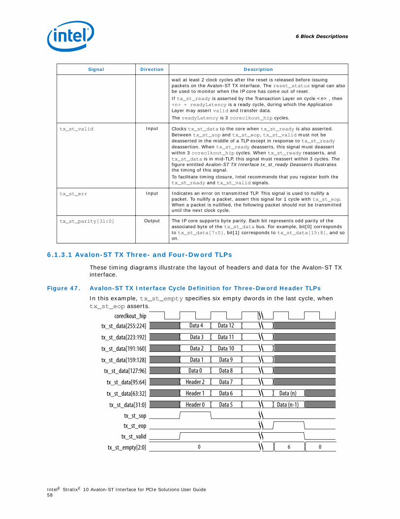
Signal Direction Description
wait at least 2 clock cycles after the reset is released before issuingpackets on the Avalon-ST TX interface. The reset_status signal can alsobe used to monitor when the IP core has come out of reset.If tx_st_ready is asserted by the Transaction Layer on cycle <n> , then<n> + readyLatency is a ready cycle, during which the ApplicationLayer may assert valid and transfer data.The readyLatency is 3 coreclkout_hip cycles.
tx_st_valid Input Clocks tx_st_data to the core when tx_st_ready is also asserted.Between tx_st_sop and tx_st_eop, tx_st_valid must not bedeasserted in the middle of a TLP except in response to tx_st_readydeassertion. When tx_st_ready deasserts, this signal must deassertwithin 3 coreclkout_hip cycles. When tx_st_ready reasserts, andtx_st_data is in mid-TLP, this signal must reassert within 3 cycles. Thefigure entitled Avalon-ST TX Interface tx_st_ready Deasserts illustratesthe timing of this signal.To facilitate timing closure, Intel recommends that you register both thetx_st_ready and tx_st_valid signals.
tx_st_err Input Indicates an error on transmitted TLP. This signal is used to nullify apacket. To nullify a packet, assert this signal for 1 cycle with tx_st_eop.When a packet is nullified, the following packet should not be transmitteduntil the next clock cycle.
tx_st_parity[31:0] Output The IP core supports byte parity. Each bit represents odd parity of theassociated byte of the tx_st_data bus. For example, bit[0] correspondsto tx_st_data[7:0], bit[1] corresponds to tx_st_data[15:8], and soon.
6.1.3.1 Avalon-ST TX Three- and Four-Dword TLPs
These timing diagrams illustrate the layout of headers and data for the Avalon-ST TXinterface.
Figure 47. Avalon-ST TX Interface Cycle Definition for Three-Dword Header TLPsIn this example, tx_st_empty specifies six empty dwords in the last cycle, whentx_st_eop asserts.
tx_st_valid
tx_st_data[127:96]
tx_st_data[95:64]
tx_st_data[63:32]
tx_st_data[31:0]
tx_st_soptx_st_eop
tx_st_empty[2:0]
Data 0 Data 8
Header 2 Data 7
Header 1 Data 6 Data (n)
Header 0 Data 5 Data (n-1)
tx_st_data[255:224]
tx_st_data[223:192]
tx_st_data[191:160]
tx_st_data[159:128]
Data 4 Data 12
Data 3 Data 11
Data 2 Data 10
Data 1 Data 9
coreclkout_hip
60 0
6 Block Descriptions
Intel® Stratix® 10 Avalon-ST Interface for PCIe Solutions User Guide58

Figure 48. Avalon-ST TX Interface Cycle Definition for Four-Dword Header TLPsIn this example, tx_st_empty specifies four empty dwords in the last cycle, whentx_st_eop asserts.
coreclkout_hip
tx_st_valid
tx_st_data[127:96]
tx_st_data[95:64]
tx_st_data[63:32]
tx_st_data[31:0]
tx_st_sop
tx_st_eop
Header3 Data 7 Data n
Header 2 Data 6 Data n-1
Header 1 Data 5 Data n-2
Header 0 Data 4 Data n-3
tx_st_data[255:224]
tx_st_data[223:192]
tx_st_data[191:160]
tx_st_data[159:128]
Data 3 Data 11
Data 2 Data 10
Data 1 Data 9
Data 0 Data 8
tx_st_empty[2:0] 40 0
6.1.3.2 Avalon-ST TX Interface tx_st_ready Deasserts
This timing diagram illustrates the timing of the TX interface when the Stratix 10 HardIP for PCI Express pauses the application by deasserting tx_st_ready. The timingdiagram shows a readyLatency of 3 cycles to facilitate timing closure. Theapplication deasserts tx_st_valid after three cycles.
Figure 49. Avalon-ST TX Interface tx_st_ready Deasserts
coreclkout_hip
tx_st_data[255:0]
tx_st_sop
tx_st_eop
tx_st_ready
tx_st_valid
tx_st_err
000 CC... CC... CC... CC... CC... CC... CC... CC... CC... CC...4 clks
3 clks
6.1.3.3 Avalon-ST TX Back-to-Back Transmission
This timing diagram illustrates back-to-back transmission on the Avalon-ST TXinterface with no idle cycles between the assertion of tx_st_eop and tx_st_sop.
Figure 50. Avalon-ST TX Back-to-Back Transmission
6 Block Descriptions
Intel® Stratix® 10 Avalon-ST Interface for PCIe Solutions User Guide59
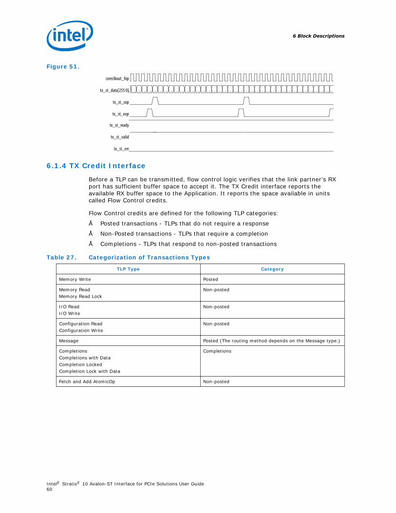
Figure 51.
coreclkout_hip
tx_st_data[255:0]
tx_st_sop
tx_st_eop
tx_st_ready
tx_st_valid
tx_st_err
.. . . . . . . . . . . . . . . . . . . . . . . . . . . . . . . . . . . . . . .
6.1.4 TX Credit Interface
Before a TLP can be transmitted, flow control logic verifies that the link partner's RXport has sufficient buffer space to accept it. The TX Credit interface reports theavailable RX buffer space to the Application. It reports the space available in unitscalled Flow Control credits.
Flow Control credits are defined for the following TLP categories:
• Posted transactions - TLPs that do not require a response
• Non-Posted transactions - TLPs that require a completion
• Completions - TLPs that respond to non-posted transactions
Table 27. Categorization of Transactions Types
TLP Type Category
Memory Write Posted
Memory ReadMemory Read Lock
Non-posted
I/O ReadI/O Write
Non-posted
Configuration ReadConfiguration Write
Non-posted
Message Posted (The routing method depends on the Message type.)
CompletionsCompletions with DataCompletion LockedCompletion Lock with Data
Completions
Fetch and Add AtomicOp Non-posted
6 Block Descriptions
Intel® Stratix® 10 Avalon-ST Interface for PCIe Solutions User Guide60

Table 28. Value of Header and Data CreditsThe following table translates credits to dwords. The PCI Express Base Specification defines a dword as fourbytes.
Credit Type Number of Dwords
Header Credit - completions 4 dwords
Header credit - requests 5 dwords
Data credits 4 dwords
Table 29. 256-Bit Avalon-ST TX DatapathThe IP core provides TX credit information to the Application Layer. To optimize performance, the Applicationcan perform credit-based checking before submitting requests for transmission, and reorder packets to improvethroughput. Reordering is optional. The IP core always checks for sufficient TX credits before transmitting anyTLP.
Signal Direction Description
tx_ph_cdts[7:0] Output Header credit net value for the flow control (FC) posted requests.
tx_pd_cdts[11:0] Output Data credit net value for the FC posted requests.
tx_nph_cdts[7:0] Output Header credit net value for the FC non-posted requests.
tx_npd_cdts[11:0] Output Data credit net value for the FC non-posted requests.
tx_cplh_cdts[7:0] Output Header credit net value for the FC Completion. A value of 0 indicatesinfinite Completion header credits.
tx_cpld_cdts[11:0] Output Data credit net value for the FC Completion. A value of 0 indicates infiniteCompletion data credit.
tx_hdr_cdts_consumed Output Asserted for 1 coreclkout_hip cycle, for each header credit consumed.Note that credits the Hard IP consumes for internally generatedCompletions or Messages are not tracked in this signal.
tx_data_cdts_consumed Output Asserted for 1 coreclkout_hip cycle, for each data credit consumed.Note that credits the Hard IP consumes for internally generatedCompletions or Messages are not tracked in this signal.
tx_cdts_type[1:0] Output Specifies the credit type shown on the tx_cdts_data_value[1:0] bus.The following encodings are defined:• 2'b00: Posted credits• 2'b01: Non-posted credits2
• 2'b10: Completion credits• 2'b11: Reserved
tx_cdts_data_value[1:0] Output The value of tx_cdts_data_value[1:0]+1 specifies the data creditconsumed when tx_data_cdts_consumed is asserted.
6.1.5 Interpreting the TX Credit Interface
The Stratix 10 PCIe TX credit interface reports the number of Flow Control creditsavailable.
The following equation defines the available buffer space:
RX_buffer_space = (credit_limit - credits_consumed)+ released_credits
2 The PCIe IP core does not consume non-posted credits.
6 Block Descriptions
Intel® Stratix® 10 Avalon-ST Interface for PCIe Solutions User Guide61

where:
credits_consumed = credits_consumedapplication + credits_consumedPCIe_IP_core
The hard IP core consumes a small number of posted credits for the following reasons:
• To send completion TLPs for Configuration Requests targeting its internal registers
• To transmit posted TLPs for error and interrupt Messages
The hard IP core does not report the internally consumed credits to the Application.Without knowing the hard IP core's internal usage, the Application cannot maintain acompletely accurate count of Posted or Completion credits.
The hard IP core does not consume non-posted credits. Consequently, it is possible tomaintain an accurate count of the available non-posted credits. Refer to the TX CreditAdjustment Sample Code for code that calculates the number of non-posted creditsavailable to the Application. This RTL recovers the updated Flow Control credits fromthe remote link. It drives value of RX_buffer_space for non-posted header and datacredits on tx_nph_cdts and tx_npd_cdts, respectively.
Figure 52. Flow Control Credit Update LoopThe following figure provides an overview of the steps to determine credits availableand release credits after the TLP is removed from the link partner's RX buffer.
Flow ControlGating Logic
(Credit Check)
CustomComputation:
RX_buf_space=((limit-consumed)
+ released)
FC UpdateDLLP Decode
FC UpdateDLLP Generate
CreditAllocated
RXBuffer
FU Update DLLP
Data PacketData
Packet
ApplicationLayer
TransactionLayer
Data LinkLayer
PhysicalLayer
PCIExpress
Link
ApplicationLayer
TransactionLayer
Data LinkLayer
PhysicalLayer
Data Source Data Sink (Link Partner)
Allow Decrement
Increment
1 2
7
6
5
43
TX CreditSignals
Note: To avoid a potential deadlock or performance degradation, the Application shouldcheck available credits before sending a TLP to the Stratix 10 Hard IP for PCI ExpressIP Core.
Related Links
TX Credit Adjustment Sample Code on page 160This sample Verilog HDL code computes the available credits for non-posted TLPs.
6 Block Descriptions
Intel® Stratix® 10 Avalon-ST Interface for PCIe Solutions User Guide62

6.1.6 Clocks
Table 30. Clocks
Signal Direction Description
refclk Input This is the input reference clock for the IP core as defined by the PCIExpress Card Electromechanical Specification Revision 2.0. Its frequency is100 MHz ±300 ppm.
coreclkout_hip Output This clock drives the Data Link, Transaction, and Application Layers. Forthe Application Layer, its frequency depends on the data rate and thenumber of lanes as specified in the table
Data Rate coreclkout_hip Frequency
Gen1 x1, x2, x4, x8, and x16 125 MHz
Gen2 x1, x2, x4, and x8, 125 MHz
Gen2 x16 250 MHz
Gen3 x1, x2, and x4 125 MHz
Gen3 x8 250 MHz
Gen3 x16 500 MHz
6.1.7 Update Flow Control Timer and Credit Release
The IP core releases credits from the RX Buffer on a per-clock-cycle basis as itremoves TLPs from the RX Buffer.
6.1.8 Resets
An embedded hard reset controller (HRC) generates the reset for PCIe core logic,PMA, PCS, and Application. To meet the 100 ms PCIe configuration time, theembedded reset controller connects to the SDM. This connection allows the FPGAperiphery to configure and begin operation before the FPGA fabric is programmed.
The reset logic requires a free running clock that is stable and available to the IP corewhen the SDM asserts iocsrrdy. A delayed version of iocsrrdy, (iocsrrdy_dly),asserts after the control and status registers are initialized and transceiverconfiguration completes.
6 Block Descriptions
Intel® Stratix® 10 Avalon-ST Interface for PCIe Solutions User Guide63

Figure 53. Stratix 10 Hard IP for PCI Express Reset ControllerThe signals shown in the Hard IP for PCIe are implemented in hard logic and notavailable for probing.
EMIB Adaptor
Self Download Mode(SDM)
PCIe IP Core
Hard IPReset
Controller
PHY(PCSand
PMA)
SDM
user
_mod
eloc
sr_rd
y fref_dk[15:0]
Hard IP for PCIe
serdes_pll_locked[15:0]pma_cal_done[15:0]rx_pma_rstbrx/tx_pcs_rstn
rst_n <n>
pld_rst_n
pld_rst_n
nporreset_statuslink_req_rst_n
pipe_clk
pin_perst_n
FPGA
Table 31. Resets
Signal Direction Description
currentspeed[1:0] Output Indicates the current speed of the PCIe link. The followingencodings are defined:• 2'b00: Undefined• 2'b01: Gen1• 2'b10: Gen2• 2'b11: Gen3
npor Input The Application Layer drives this active low reset signal. npor resets theentire IP core, PCS, PMA, and PLLs. npor should be held for a minimum of20 ns. Gen3 x16 variants, should hold npor for at least 10 cycles. Thissignal is edge, not level sensitive; consequently, a low value on this signaldoes not hold custom logic in reset. This signal cannot be disabled.
pin_perst Input Active low reset from the PCIe reset pin of the device. Resets the datapathand control registers.
pld_clk_inuse Output This reset signal has the same effect as reset_status. This signal isprovided for backwards compatibility with Arria 10 devices.
pld_core_ready Input When asserted, indicates that the Application Layer is ready. The IP corecan releases reset after this signal is asserted.
continued...
6 Block Descriptions
Intel® Stratix® 10 Avalon-ST Interface for PCIe Solutions User Guide64

Signal Direction Description
reset_status Output Active high reset status. When high, indicates that the IP core is not readyfor usermode. reset_status is deasserted only when npor isdeasserted and the IP core is not in reset. Use reset_status to drivethe reset of your application. Synchronous to coreclkout_hip.
clr_st Output clr_st has the same functionality as reset_status. It is provided forbackwards compatibility with previous device families.
serdes_pll_locked Output When asserted, indicates that the PLL that generates coreclkout_hip islocked. In pipe simulation mode this signal is always asserted.
6.1.9 Interrupts
6.1.9.1 MSI Interrupts
Message Signaled Interrupts (MSI) interrupts are signaled on the PCI Express linkusing a single dword Memory Write TLP.
Table 32. MSI
Signal Direction Description
app_msi_req Input Application Layer MSI request. Assertion causes an MSI posted write TLPto be generated based on the MSI configuration register values and theapp_msi_tc and app_msi_num input ports. Deasserts whenapp_msi_ack acknowledges the request.
app_msi_ack Output Application Layer MSI acknowledge. Asserts for 1 cycle to acknowledge theApplication Layer's request for an MSI interrupt.
app_msi_tc[2:0] Input Application Layer MSI traffic class. This signal indicates the traffic classused to send the MSI (unlike INTX interrupts, any traffic class can be usedto send MSIs).
app_msi_num[4:0] Input MSI number of the Application Layer. This signal provides the low ordermessage data bits to be sent in the message data field of MSI messagesrequested by app_msi_req. Only bits that are enabled by the MSIMessage Control register apply.
6.1.9.2 Legacy Interrupts
Legacy interrupts mimic the original PCI level-sensitive interrupts using virtual wiremessages. The term, INTx, refers collectively to the four legacy interrupts, INTA#,INTB#, INTC# and INTD#.
6 Block Descriptions
Intel® Stratix® 10 Avalon-ST Interface for PCIe Solutions User Guide65

Table 33. Legacy Interrupts (MSI)
Signal Direction Description
app_int_sts Input Controls legacy interrupts. Assertion of app_int_sts causes anAssert_INTx message TLP to be generated and sent upstream. Deassertionof app_int_sts causes a Deassert_INTx message TLP to be generatedand sent upstream.
int_status[3:0] Output int_status[3:0] drives legacy interrupts to the Application Layer asfollows:• int_status[0]: interrupt signal A• int_status[1]: interrupt signal B• int_status[2]: interrupt signal C• int_status[3]: interrupt signal D
int_status_common[2:0] Output Specifies the interrupt status for the following registers. When asserted,indicates that an interrupt is pending:• int_status_common[0]: Autonomous bandwidth status register.• int_status_common[1]: Bandwidth management status register.• int_status_common[2]: Link equalization request bit in the link
status register.
6.1.10 Transaction Layer Configuration Space Interface
The Transaction Layer (TL) bus provides a subset of the information stored in theConfiguration Space. Use this information in conjunction with the app_err* signals tounderstand TLP transmission problems.
Table 34. Configuration Space Signals
Signal Direction Description
tl_cfg_add[4:0] Output Address of the TLP register. This signal is an index indicating whichConfiguration Space register information is being driven ontotl_cfg_ctl. Refer to Multiplexed Configuration Register InformationAvailable on tl_cfg_ctl for the available information.
tl_cfg_ctl[31:0] Output The tl_cfg_ctl signal is multiplexed and contains a subset of contentsof the Configuration Space registers.
tl_cfg_func[1:0] Output Specifies the function whose Configuration Space register values are beingdriven tl_cfg_ctl[31:0]. The following encodings are defined:• 2'b00: Physical Function (PF0)• 2'b01: Reserved for L-tile; PF1 for H-Tile• 2'b10: Reserved for L-tile; Virtual Functions (VF) for H-Tile• 2'b11: Reserved
app_err_hdr[31:0] Input Header information for the error TLP. Four, 4-byte transfers send thisinformation to the IP core.
app_err_info[10:0] Input The Application can optionally provide the following information:• app_err_info[0]: Malformed TLP• app_err_info[1]: Receiver Overflow• app_err_info[2]: Unexpected Completion• app_err_info[3]: Completer Abort• app_err_info[4]: Completer Timeout• app_err_info[5]: Unsupported Request• app_err_info[6]: Poisoned TLP Received• app_err_info[7]: AtomicOp Egress Blocked
continued...
6 Block Descriptions
Intel® Stratix® 10 Avalon-ST Interface for PCIe Solutions User Guide66

Signal Direction Description
• app_err_info[8]: Uncorrectable Internal Error• app_err_info[9]: Correctable Internal Error• app_err_info[10]: Advisory Non-Fatal Error
app_err_valid Input When asserted, indicates that the data on app_err_info[10:0] is valid.
Figure 54. Configuration Space Register Access TimingInformation on the Transaction Layer (TL) bus is time-division multiplexed (TDM).When tl_cfg_func[1:0]= 2'b00, tl_cfg_ctl[31:0] drives PF0 ConfigurationSpace register values for eight consecutive cycles. The next 40 cycles driveinformation for PF1 and the VFs which are not supported in the current release. Then,the 48-cycle pattern repeats.
coreclkout_hip
Cycle:
tl_cfg_ctl[31:0]
tl_cfg_add[4:0]
tl_cfg_func[1:0]
0 1 2 3 4 5 6
1 2 3 4 5 6
7 0 6 7 0
0=PF0 0=PF0
Cycle4Cycle0 Cycle1 Cycle3Cycle2 Cycle5 Cycle6 Cycle8Cycle7 Cycle46 Cycle48Cycle47
0 8 487 4746
Table 35. Multiplexed Configuration Register Information Available on tl_cfg_ctl
TDM
31 24 23 16 15 8 7 0
0 [28:24] Device Number Bus Number Reserved Device Control[2:0]: Max payload size[5:3]: Max rd req size[6]: Extended tag enable[7]: Bus master enable
1 [28:24]AER IRQ msg num [16]: RCB cntl[17]: cfg_pm_no_soft_rst
PCIe capability IRQ msgnum[20:16]
[1:0]: Sys power ind. cntl[3:2]: Sys atten ind cntl[4]: Sys power cntl
2 Index of 1st VF Num VFs Reserved [0]: VF enable[2:1]: TPH[3]: Atomic req en[4:] AtomicOp egress block[5]: ARI forward enable[6]: End-End TLP prefixblocking
3 MSI Address Lower
4 MSI Address Upper
5 MSI Mask
6 MSI Data Reserved [0]: MSI enable[1]: 64-bit MSI[4:2]: Multiple MSI enable
7 Reserved
6 Block Descriptions
Intel® Stratix® 10 Avalon-ST Interface for PCIe Solutions User Guide67

6.1.11 Configuration Extension Bus Interface
Use the Configuration Extension Bus to add capability structures to the IP core’sinternal Configuration Spaces. Configuration TLPs with a destination register byteaddress of 0xC00 and higher are routed to the Configuration Extension Bus interface.Report the Completion Status Successful Completion (SC) on the ConfigurationExtension Bus. The IP core then generates a Completion to transmit on the link.Use the app_err_info[8] signal included in the Transaction Layer ConfigurationSpace Interface to report uncorrectable internal errors.
Note: The IP core does not apply ID-based Ordering (IDO) bits to the internally generatedCompletions.
Signal Direction Description
ceb_req Output When asserted, indicates a valid Configuration Extension Bus access cycle.Deasserted when ceb_ack is asserted.
ceb_ack Input Asserted to acknowledged ceb_req. The Application must implement thislogic.
ceb_addr[11:0] Output Address bus to the external register block. The width of the address bus isthe value you select for the CX_LBC_EXT_AW parameter.
ceb_din[31:0] Input Read data.
ceb_dout[31:0] Output Data to be written.
ceb_wr[3:0] Output Indicates the configuration register access type, read or write. For writes,CEB_wr also indicates the byte enables: The following encodings aredefined:• 4'b000: Read• 4'b0001: Write byte 0• 4'b0010: Write byte 1• 4'b0100: Write byte 2• 4'b1000: Write byte 3• 4'b1111: Write all bytes.Combinations of byte enables, for example,4'b 0101b are also valid.
6.1.12 Hard IP Status Interface
Hard IP Status: This optional interface includes the following signals that are useful fordebugging, including: link status signals, interrupt status signals, TX and RX parityerror signals, correctable and uncorrectable error signals.
Table 36. Hard IP Status Interface
Signal Direction Description
derr_cor_ext_rcv Output When asserted, indicates that the RX buffer detected a 1-bit (correctable)ECC error. This is a pulse stretched output.
derr_cor_ext_rpl Output When asserted, indicates that the retry buffer detected a 1-bit(correctable) ECC error. This is a pulse stretched output.
derr_rpl Output When asserted, indicates that the retry buffer detected a 2-bit(uncorrectable) ECC error. This is a pulse stretched output.
derr_uncor_ext_rcv Output When asserted, indicates that the RX buffer detected a 2-bit(uncorrectable) ECC error. This is a pulse stretched output.
continued...
6 Block Descriptions
Intel® Stratix® 10 Avalon-ST Interface for PCIe Solutions User Guide68

Signal Direction Description
int_status[3:0] Output Drives legacy interrupts to the Application Layer as follows:• int_status[0]: interrupt signal A
• int_status[1]: interrupt signal B• int_status[2]: interrupt signal C• int_status[3]: interrupt signal D
int_status_common[2:0] Output Specifies the interrupt status for the following registers. When asserted,indicates that an interrupt is pending:• int_status_common[0]: Autonomous bandwidth status register.• int_status_common[1]: Bandwidth management status register.• int_status_common[2]: Link equalization request bit in the link
status register.
lane_act[4:0] Output Lane Active Mode: This signal indicates the number of lanes thatconfigured during link training. The following encodings are defined:• 5’b0 0001: 1 lane• 5’b0 0010: 2 lanes• 5’b0 0100: 4 lanes• 5’b0 1000: 8 lanes• 5'b1 0000: 16 lanes
link_up Output When asserted, the link is up.
ltssmstate[5:0] Output LTSSM state: The LTSSM state machine encoding defines the followingstates:• 6'h00 - Detect.Quiet• 6'h01 - Detect.Active• 6'h02 - Polling.Active• 6'h03 - Polling.Compliance• 6'h04 - Polling.Configuration• 6'h05 - PreDetect.Quiet• 6'h06 - Detect.Wait• 6'h07 - Configuration.Linkwidth.Start• 6'h08 - Configuration.Linkwidth.Accept• 6'h09 - Configuration.Lanenum.Wait• 6'h0A - Configuration.Lanenum.Accept• 6'h0B - Configuration.Complete• 6'h0C - Configuration.Idle• 6'h0D - Recovery.RcvrLock• 6'h0E - Recovery.Speed• 6'h0F - Recovery.RcvrCfg• 6'h10 - Recovery.Idle• 6'h20 - Recovery.Equalization Phase 0• 6'h21 - Recovery.Equalization Phase 1• 6'h22 - Recovery.Equalization Phase 2• 6'h23 - Recovery.Equalization Phase 3• 6'h11 - L0• 6'h12 - L0s• 6'h13 - L123.SendEIdle• 6'h14 - L1.Idle• 6'h15 - L2.Idle• 6'h16 - L2.TransmitWake• 6'h17 - Disabled.Entry• 6'h18 - Disabled.Idle• 6'h19 - Disabled• 6'h1A - Loopback.Entry
continued...
6 Block Descriptions
Intel® Stratix® 10 Avalon-ST Interface for PCIe Solutions User Guide69

Signal Direction Description
• 6'h1B - Loopback.Active• 6'h1C - Loopback.Exit• 6'h1D - Loopback.Exit.Timeout• 6'h1E - HotReset.Entry• 6'h1F - Hot.Reset
rx_par_err Output Asserted for a single cycle to indicate that a parity error was detected in aTLP at the input of the RX buffer. This error is logged as an uncorrectableinternal error in the VSEC registers. For more information, refer toUncorrectable Internal Error Status Register. If this error occurs, you mustreset the Hard IP because parity errors can leave the Hard IP in anunknown state.
tx_par_err Output Asserted for a single cycle to indicate a parity error during TX TLPtransmission. The IP core transmits TX TLP packets even when a parityerror is detected.
Related Links
Uncorrectable Internal Error Status Register on page 96This register reports the status of the internally checked errors that areuncorrectable.
6.1.13 Serial Data Interface
The IP core supports 1, 2, 4, 8, or 16 lanes.
Table 37. Serial Data Interface
Signal Direction Description
tx_out Output Transmit serial data output.
rx_in Input Receive serial data input.
6.1.14 PIPE Interface
The Stratix 10 PIPE interface compiles with the PHY Interface for the PCI ExpressArchitecture PCI Express 3.0 specification.
Signal Direction Description
txdata[31:0] Output Transmit data.
txdatak[3:0] Output Transmit data control.
txcompl Output Transmit compliance. This signal drives the TX compliance pattern. Itforces the running disparity to negative in Compliance Mode (negativeCOM character).
txelecidle Output Transmit electrical idle. This signal forces the TX output to electrical idle.
txdetectrx Output Transmit detect receive. This signal tells the PHY layer to start a receivedetection operation or to begin loopback.
powerdown[1:0] Output Power down. This signal requests the PHY to change its power state to thespecified state (P0, P0s, P1, or P2).
txmargin[2:0] Output Transmit VOD margin selection. The value for this signal is based on thevalue from the Link Control 2 Register.
continued...
6 Block Descriptions
Intel® Stratix® 10 Avalon-ST Interface for PCIe Solutions User Guide70

Signal Direction Description
txdeemp Output Transmit de-emphasis selection. The Stratix 10 Hard IP for PCI Expresssets the value for this signal based on the indication received from theother end of the link during the Training Sequences (TS). You do not needto change this value.
txswing Output When asserted, indicates full swing for the transmitter voltage. Whendeasserted indicates half swing.
txsynchd[1:0] Output For Gen3 operation, specifies the receive block type. The followingencodings are defined:• 2'b01: Ordered Set Block• 2'b10: Data BlockDesigns that do not support Gen3 can ground this signal.
txblkst[3:0] Output For Gen3 operation, indicates the start of a block in the transmit direction.pipe spec
txdataskip Output For Gen3 operation. Allows the MAC to instruct the TX interface to ignorethe TX data interface for one clock cycle. The following encodings aredefined:• 1’b0: TX data is invalid• 1’b1: TX data is valid
rate[1:0] Output The 2-bit encodings have the following meanings:• 2’b00: Gen1 rate (2.5 Gbps)• 2’b01: Gen2 rate (5.0 Gbps)• 2’b1X: Gen3 rate (8.0 Gbps)
rxpolarity Output Receive polarity. This signal instructs the PHY layer to invert the polarity ofthe 8B/10B receiver decoding block.
currentrxpreset[2:0] Output For Gen3 designs, specifies the current preset.
currentcoeff[17:0] Output For Gen3, specifies the coefficients to be used by the transmitter. The 18bits specify the following coefficients:• [5:0]: C-1
• [11:6]: C0
• [17:12]: C+1
rxeqeval Output For Gen3, the PHY asserts this signal when it begins evaluation of thetransmitter equalization settings. The PHY asserts Phystatus when itcompletes the evaluation. The PHY deasserts rxeqeval to abortevaluation.Refer to the figure below for a timing diagram illustrating this process.
rxeqinprogress Output For Gen3, the PHY asserts this signal when it begins link training. The PHYlatches the initial coefficients from the link partner.Refer to the figure below for a timing diagram illustrating this process.
invalidreq Output For Gen3, indicates that the Link Evaluation feedback requested a TXequalization setting that is out-of-range. The PHY asserts this signalcontinually until the next time it asserts rxeqeval.
rxdata[31:0] Input Receive data control. Bit 0 corresponds to the lowest-order byte ofrxdata, and so on. A value of 0 indicates a data byte. A value of 1indicates a control byte. For Gen1 and Gen2 only.
rxdatak[3:0] Input Receive data control. This bus receives data on lane. Bit 0 corresponds tothe lowest-order byte of rxdata, and so on. A value of 0 indicates a databyte. A value of 1 indicates a control byte. For Gen1 and Gen2 only.
phystatus Input PHY status. This signal communicates completion of several PHY requests.pipe spec
continued...
6 Block Descriptions
Intel® Stratix® 10 Avalon-ST Interface for PCIe Solutions User Guide71

Signal Direction Description
rxvalid Input Receive valid. This signal indicates symbol lock and valid data on rxdataand rxdatak.
rxstatus[2:0] Input Receive status. This signal encodes receive status, including error codesfor the receive data stream and receiver detection.
rxelecidle Input Receive electrical idle. When asserted, indicates detection of an electricalidle. pipe spec
rxsynchd[3:0] Input For Gen3 operation, specifies the receive block type. The followingencodings are defined:• 2'b01: Ordered Set Block• 2'b10: Data BlockDesigns that do not support Gen3 can ground this signal.
rxblkst[3:0] Input For Gen3 operation, indicates the start of a block in the receive direction.
rxdataskip Input For Gen3 operation. Allows the PCS to instruct the RX interface to ignorethe RX data interface for one clock cycle. The following encodings aredefined:• 1’b0: RX data is invalid• 1’b1: RX data is valid
dirfeedback[5:0] Input For Gen3, provides a Figure of Merit for link evaluation for H tiletransceivers. The feedback applies to the following coefficients:• dirfeedback[5:4]: Feedback applies to C+1
• dirfeedback[3:2]: Feedback applies to C0
• dirfeedback[1:0]: Feedback applies to C-1
The following feedback encodings are defined:• 2'b00: No change• 2'b01: Increment• 2'b10: Decrement• 2/b11: ReservedRefer to the figure below for a timing diagram illustrating this process.
simu_mode_pipe Input When set to 1, the PIPE interface is in simulation mode.
sim_pipe_pclk_in Input This clock is used for PIPE simulation only, and is derived from the refclk.It is the PIPE interface clock used for PIPE mode simulation.
sim_pipe_rate[1:0] Output The 2-bit encodings have the following meanings:• 2’b00: Gen1 rate (2.5 Gbps)• 2’b01: Gen2 rate (5.0 Gbps)• 2’b10: Gen3 rate (8.0 Gbps)
sim_ltssmstate[5:0] Output LTSSM state: The following encodings are defined:• 6'h00 - Detect.Quiet• 6'h01 - Detect.Active• 6'h02 - Polling.Active• 6'h03 - Polling.Compliance• 6'h04 - Polling.Configuration• 6'h05 - PreDetect.Quiet• 6'h06 - Detect.Wait• 6'h07 - Configuration.Linkwidth.Start• 6'h08 - Configuration.Linkwidth.Accept• 6'h09 - Configuration.Lanenum.Wait• 6'h0A - Configuration.Lanenum.Accept• 6'h0B - Configuration.Complete• 6'h0C - Configuration.Idle• 6'h0D - Recovery.RcvrLock
continued...
6 Block Descriptions
Intel® Stratix® 10 Avalon-ST Interface for PCIe Solutions User Guide72

Signal Direction Description
• 6'h0E - Recovery.Speed• 6'h0F - Recovery.RcvrCfg• 6'h10 - Recovery.Idle• 6'h20 - Recovery.Equalization Phase 0• 6'h21 - Recovery.Equalization Phase 1• 6'h22 - Recovery.Equalization Phase 2• 6'h23 - Recovery.Equalization Phase 3• 6'h11 - L0• 6'h12 - L0s• 6'h13 - L123.SendEIdle• 6'h14 - L1.Idle• 6'h15 - L2.Idle• 6'h16 - L2.TransmitWake• 6'h17 - Disabled.Entry• 6'h18 - Disabled.Idle• 6'h19 - Disabled• 6'h1A - Loopback.Entry• 6'h1B - Loopback.Active• 6'h1C - Loopback.Exit• 6'h1D - Loopback.Exit.Timeout• 6'h1E - HotReset.Entry• 6'h1F - Hot.Reset
sim_pipe_mask_tx_pll_lock
Input Should be active during rate change. This signal Is used to mask the PLLlock signals. This interface is used only for PIPE simulations.In serial simulations, The Endpoint PHY drives this signal. For PIPEsimulations, in the Intel testbench, The PIPE BFM drives this signal.
Related Links
PHY Interface for the PCI Express Architecture PCI Express 3.0
6.1.15 Hard IP Reconfiguration
The Hard IP reconfiguration interface is an Avalon-MM slave interface with a 21-bitaddress and an 8-bit data bus. You can use this bus to dynamically modify the valueof configuration registers that are read-only at run time.To ensure proper systemoperation, reset or repeat device enumeration of the PCI Express link after changingthe value of read-only configuration registers of the Hard IP.
Table 38. Hard IP Reconfiguration Signals
Signal Direction Description
hip_reconfig_clk Input Reconfiguration clock. The frequency range for this clock is 100–125 MHz.
hip_reconfig_rst_n Input Active-low Avalon-MM reset for this interface.
hip_reconfig_address[20:0] Input The 21-bit reconfiguration address.
hip_reconfig_read Input Read signal. This interface is not pipelined. You must wait for thereturn of the hip_reconfig_readdata[7:0] from the current readbefore starting another read operation.
hip_reconfig_readdata[7:0] Output 8-bit read data. hip_reconfig_readdata[7:0] is valid on thethird cycle after the assertion of hip_reconfig_read.
continued...
6 Block Descriptions
Intel® Stratix® 10 Avalon-ST Interface for PCIe Solutions User Guide73

Signal Direction Description
hip_reconfig_readdatavalid Output When asserted, the data on hip_reconfig_readdata[7:0] isvalid.
hip_reconfig_write Input Write signal.
hip_reconfig_writedata[7:0] Input 8-bit write model.
hip_reconfig_waitrequest Output When asserted, indicates that the IP core is not ready to respond to arequest.
6.1.16 Power Management Interface
Software programs the Device into a D-state by writing to the Power ManagementControl and Status register in the PCI Power Management Capability Structure. The IPcore supports the required PCI D0 and D3 Power Management states. D1 and D2states are not supported.
Table 39. Power Management Interface Signals
Signal Direction Description
pm_linkst_in_l1 Output When asserted, indicates that the link is in the L1 state.
pm_linkst_in_l0s Output When asserted, indicates that the link is in the L0s state.
pm_state[2:0] Output Specifies the current power state.
pm_dstate[2:0] Output Specifies the power management D-state for PF0.
apps_pm_xmt_pme Input Wake Up. The Application Layer asserts this signal for 1 cycle to wake upthe Power Management Capability (P MC) state machine from a D1, D2 orD3 power state. Upon wake-up, the core sends a PM_PME Message. Thisport is functionally identical to outband_pwrup_cmd. You can use thissignal or outband_pwrup_cmd to request a return from a low-powerstate to D0.
apps_ready_entr_l23 Input When asserted, the data on hip_reconfig_readdata[7:0] is valid.
apps_pm_xmt_turnoff Input Application Layer request to generate a PM_Turn_Off message. TheApplication Layer must assert this signal for one clock cycle. The IP coredoes not return an acknowledgment or grant signal. The Application Layermust not pulse this signal again until the previous message has beentransmitted.
app_init_rst Input Application Layer request for a hot reset to downstream devices.
app_xfer_pending Input When asserted, prevents the IP core from entering L1 state or initiatesexit from the L1 state.
6.1.17 Test Interface
The 256-bit test output interface is available only for x16 simulations. For x1, x2, x4,and x8 variants a 7-bit auxiliary test bus is available.
6 Block Descriptions
Intel® Stratix® 10 Avalon-ST Interface for PCIe Solutions User Guide74

Signal Direction Description
test_int[66:0] Input This is a multiplexer to selects the test_out[255:0] and aux_test_out[6:0]buses. Driven from channels 8-15.The following encodings are defined:• [66:1]: Reserved• [0]: Turns on diag_fast_link_mode to speed up simulation.
testin_zero Output When asserted, indicates accelerated initialization for simulation is active.
6 Block Descriptions
Intel® Stratix® 10 Avalon-ST Interface for PCIe Solutions User Guide75

6.1.18 Message Handling
6.1.18.1 Endpoint Received Messages
Message Type Message Message Processing
Power Management PME_Turn_Off Forwarded to the Application Layer on Avalon-ST RX interface. Alsoprocessed by the IP core.
Slot Power Limit Set_Slot_Power_Limit Forwarded to the Application Layer on Avalon-ST RX interface.
Vendor Defined withor without Data
Vendor_Type0 Forwarded to the Application Layer on Avalon-ST RX interface. Notprocessed by core.You can program the IP core to drop these Messages using thevirtual_drop_vendor0_msg. When dropped, Vendor0 Messages arelogged as Unsupported Requests (UR).
ATS ATS_Invalidate Forwarded to the Application Layer on Avalon-ST RX interface. Notprocessed by the IP core.
Locked Transaction Unlock Message Forwarded to the Application Layer on Avalon-ST RX interface. Notprocessed by the IP core.
All Others --- Internally dropped by Endpoint and handled as an Unsupported Request.
6.1.18.2 Endpoint Transmitted Messages
The Endpoint transmits Messages that it receives from the Application Layer on theAvalon-ST TX interface and internally generated messages. The Endpoint maygenerate Messages autonomously or in response to a request received on the :app_pm_xmt_pme, app_int, or app_err_* input ports.
Message Type Message Message Processing
Power Management PM_PME, PME_TO_Ack The Application Layer transmits the PM_PME request via theapp_pm_xmt_pme input.The Application Layer must generate the PME_TO_Ack and transmit it onthe Avalon-ST TX interface.The Application Layer transmits the app_ready_entr_l23 to indicate that itis ready to enter the L23 state.
Vendor Defined withor without Data
Vendor_Type0 The Application Layer must generate and transmit this on the Avalon-STTX interface.
ATS ATS_Request,ATS_InvalidateCompletion
The Application Layer must generate and transmit these Messages on theAvalon-ST TX interface.
INT INTx_Assert,INTx_Deassert
The Application Layer transmits the INTx_Assert and INTx_DeassertMessages using the app_int interface.
ERR ERR_COR,ERR_NONFATAL,ERR_FATAL
The IP core transmits these error Messages autonomously when it detectsinternal errors. It also receives and forwards these errors when receivedfrom the Application Layer via the app_err_* interface.
6.1.18.3 Root Port Received Messages
The Root Port forwards Messages received to the Application Layer on the Avalon-STRX interface. It also reflects legacy interrupts on the dedicated INTx interface anderror messages on the app_err_* interface.
6 Block Descriptions
Intel® Stratix® 10 Avalon-ST Interface for PCIe Solutions User Guide76

Note: Root Ports are not supported in the Quartus Prime Pro – Stratix 10 Edition 17.1Interim Release.
Message Type Message Message Processing
PowerManagement
PM_PME,PME_TO_Ack
Forwarded to the Application Layer on the Avalon-RX interface. Alsoprocessed by the IP core.
Vendor Definedwith or withoutData
Vendor_Type0 Forwarded to the Application Layer on the Avalon-RX interface. Notprocessed by the IP core.You can program the IP core to drop these Messages using thevirtual_drop_vendor0_msg. When dropped, Vendor0 Messages arelogged as Unsupported Requests (UR).
ATS ATS_Request,ATS_InvalidateCompletion
Forwarded to the Application Layer on the Avalon-RX interface. Notprocessed by the IP core
INT INTx_Assert,INTx_Deassert
Processed by the IP core. The IP core transmits these Messages on theint_status_* interface. Forwarded to the Application Layer on the Avalon-RX interface.
ERR ERR_CORR,ERR_NONFATAL,ERR_FATAL
Processed by the IP core. The IP core transmits these Messages on theapp_err_* interface. Forwarded to the Application Layer on the Avalon-RXinterface.
All Others N/A The Root Port drops this messages and handles them as UnsupportedRequests (UR).
6.1.18.4 Root Port Transmitted Messages
The Root Port forwards Messages received from the Application Layer on its Avalon-STTX interface. It also transmits also generates Messages autonomously or in responseto Messages received on a dedicated Power Management interface.
Note: Root Ports are not supported in the Quartus Prime Pro – Stratix 10 Edition 17.1Interim Release.
Message Type Message Message Processing
Power Management PME_Turn_Off Application requests this Message via the app_pm_xmt_turnoff input.
Slot Power Limit Set_Slot_Power_Limit The IP core transmits this Message whenever the Slot Capabilities registeris written or when the LTSSM enters L0.
Vendor Defined withor without Data
Vendor_Type0 The Root Port forwards Messages received from the Application Layer. TheApplication must assemble the TLP and transmit it via the Avalon-ST TXinterface.
ATS ATS_Invalidate The Root Port forwards Messages received from the Application Layer. TheApplication must assemble the TLP and transmit it via the Avalon-ST TXinterface.
Locked Transaction Unlock Message The Root Port forwards Messages received from the Application Layer. TheApplication must assemble the TLP and transmit it via the Avalon-ST TXinterface.
6.2 Errors reported by the Application Layer
The Application Layer uses the app_err_* interface to report errors to the IP core.
6 Block Descriptions
Intel® Stratix® 10 Avalon-ST Interface for PCIe Solutions User Guide77
The Application Layer reports the following types of errors to the IP core:
• Unexpected Completion
• Completer Abort
• CPL Timeout
• Unsupported Request
• Poisoned TLP received
• Uncorrected Internal Error, including ECC and parity errors flagged by the core
• Corrected Internal Error, including Corrected ECC errors flagged by the core
• Advisory NonFatal Error
For Advanced Error Reporting (AER), the Application Layer provide the information tolog the TLP header and the error log request via the app_err_* interface.
The Application Layer completes the following steps to report an error to the IP core:
• Sets the corresponding status bits in the PCI Status register, and the PCIeDevice Status register
• Sets the appropriate status bits and header log in the AER registers if AER isenabled
• Indicates the Error event to the upstream component:
— Endpoints transmit an Message upstream
— Root Ports assert app_serr_out to the Application Layer if an error isdetected or if an error Message is received from a downstream component.The Root Port also forwards the error Message from the downstreamcomponent on the Avalon-ST RX interface. The Application Layer may chooseto ignore this information. (Root Ports are not supported in the Quartus PrimePro – Stratix 10 Edition 17.1 Interim Release.)
6.2.1 Error Handling
When the IP core detects an error in a received TLP, it generates a Completion. It setsthe Completion status set to Completer Abort (CA) or Unsupported Request (UR).
6 Block Descriptions
Intel® Stratix® 10 Avalon-ST Interface for PCIe Solutions User Guide78

The IP Core completes the following actions when it detects an error in a received TLP:
• Discards the TLP.
• Generates a Completion (for non-posted requests) with the Completion status setto CA or UR.
• Sets the corresponding status bits in the PCI Status register and the PCIeDevice Status register.
• Sets the corresponding status bits and header log in the AER registers if AER isenabled.
• Indicates the Error event to the upstream component.
— For Endpoints, the IP core sends an error Message upstream.
— For Root Ports, the IP core asserts app_serr_out asserts to the ApplicationLayer) when it detects an error or receives an error Message from adownstream component.
Note: The error Message from the downstream component is also forwardedon the Avalon-ST RX interface. The Application Layer may choose toignore this information.
6.3 Power Management
The Stratix 10 Hard IP for PCI Express IP core supports the required PCI D0 and D3Power Management states. It does not support the optional D1 and D2 PowerManagement states.
Software programs the Device into a D-state by writing to the Power ManagementControl and Status register in the PCI Power Management Capability Structure.The pm_* interface transmits the D-state to the Application Layer.
6.3.1 Endpoint D3 Entry
This topic outlines the D3 power-down procedure.
All transmission on the Avalon-ST TX and RX interfaces must have completed beforeIP core can begin the L1 request (Enter_L1 DLLP). In addition, the RX Buffer must beempty and the Application Layer app_xfer_pending output must be deasserted.
1. Software writes the Power Management Control register to put the IP core to theD3hot state.
2. The Endpoint stops transmitting requests when it has been taken out of D0.
3. The link transitions to L1.
4. Software sends the PME_Turn_Off Message to the Endpoint to initiate power down.The Root Port transitions the link back to L0, and Endpoint receives the Messageon the Avalon-ST RX interface.
5. The End Point transmits a PME_TO_Ack Message to acknowledge the Turn Offrequest.
6. When ready for power removal, (D3cold), the End Point assertsapp_ready_entr_l23. The core sends the PM_Enter_L23 DLLP and initiates theLink transition to L3.
6 Block Descriptions
Intel® Stratix® 10 Avalon-ST Interface for PCIe Solutions User Guide79

6.3.2 End Point D3 Exit
An End Point can exit the D3 state if the following two conditions are true: First, thePME_Support setting in the Power Management Capabilities (PMC) registermust enable PME notification. Second, software must set the PME_en bit in the PowerManagement Control and Status (PMCSR) register.
6.3.3 Exit from D3 hot
The Power Management Capability register must enable D3Hot PME_Support.In addition, software must set the PME_en bit in the Power Management Controland Status register.
6.3.4 Exit from D3 cold
1. To issue a PM_EVENT Message from the D3 cold state, the device must first issuea wakeup event (WAKE#) to request reapplication of power and the clock.The wakeup event triggers a fundamental reset which reinitializes the link to L0.
2. The Application Layer requests a wake-up event by asserting apps_pm_xmt_pme.Asserting apps_pm_xmt_pme causes the IP core to transmit a PM_EVENTMessage. In addition, the IP core sets the PME_status bit in the PowerManagement Control and Status register to notify software that it hasrequested the wakeup.
The PCIe Link states are indicated on the pm_* interface. The LTSSM state isindicated on the ltssm_state output.
6.3.5 Active State Power Management
Active State Power Management (ASPM) is not supported as indicated by the ASPMSupport bits in the Link Capabilities register.
6.4 Transaction Ordering
6.4.1 TX TLP Ordering
TLPs on the Avalon-ST TX interface are transmitted in the order in which theApplication Layer presents them. The IP core provides TX credit information to theApplication Layer so that the Application Layer can perform credits-based reorderingbefore submitting TLPs for transmission.
This reordering is optional. The IP core always checks for sufficient TX credits beforetransmitting any TLP. Ordering is not guaranteed between the following TLPtransmission interfaces:
• Avalon
• MSI and MSI-X interrupt
• Internal Configuration Space TLPs
6 Block Descriptions
Intel® Stratix® 10 Avalon-ST Interface for PCIe Solutions User Guide80
6.4.2 RX TLP Ordering
TLPs ordering on the Avalon-ST RX interface is determined by the available credits foreach TLP type and the PCIe ordering rules. Refer to Table 2-34 Ordering RulesSummary in the PCI Express Base Specification Revision 3.0 for a summary of theordering rules.
The IP core implements relaxed ordering as described in the PCI Express BaseSpecification Revision 3.0. It does not perform ID-Based Ordering (IDO). TheApplication Layer can implement IDO reordering. It is possible for two different TLPtypes pending in the RX buffer to have equal priority. When this situation occurs, theIP core uses a fairness-based arbitration scheme to determine which TLP to forward tothe Application Layer.
Related Links
PCI Express Base Specification 3.0
6.5 RX Buffer
The Receive Buffer stores TLPs received from the PCI Express link. The RX Bufferstores the entire TLP before it forwards it to the Application Layer.Storing the entire TLP allows the IP to accomplish two things:
• The IP core can rate match the PCIe link to the Application Layer.
• The IP core can store TLPs until error checking is complete.
The 64 KB RX buffer has separate buffer space for Posted, Non-Posted and CompletionTLPS. Headers and data also have separate allocations. The RX Buffer enables fullbandwidth RX traffic for all three types of TLPs simultaneously.
Table 40. Flow Control Credit AllocationThe buffer allocation is fixed.
RX Buffer Segment Number of Credits Buffer Size
Posted Posted headers: 127 creditsPosted data: 750 credits
~14 KB
Non-posted Non-posted headers credits: 115 creditsNon-posted data credits: 230 credits
~5.5 KB
Completions Completion headers: 770 creditsCompletion data: 2500 credits
~50 KB
The RX buffer operates only in the Store and Forward Queue Mode. Bypass and Cut-through modes are not supported.
Flow control credit checking for the posted and non-posted buffer segments preventsRX buffer overflow. The PCI Express Base Specification Revision 3.0 requires the IPcore to advertise infinite Completion credits. The Application Layer must manage itsRead Requests so as not to overflow the Completion buffer segment.
Related Links
PCI Express Base Specification 3.0
6 Block Descriptions
Intel® Stratix® 10 Avalon-ST Interface for PCIe Solutions User Guide81

6.5.1 Retry Buffer
The retry buffer stores a copy of a transmitted TLP until the remote deviceacknowledges the TLP using the ACK mechanism. In the case of an LCRC error on thereceiving side, the remote device sends NAK DLLP to the transmitting side. Thetransmitting side retrieves the TLP from the retry buffer and resends it.
Retry buffer resources are only freed upon reception of an ACK DLLP.
6.5.2 Configuration Retry Status
The Stratix 10 Hard IP for PCI Express is part of the periphery image of the device.After power-up, the periphery image is loaded first. The End Point can then respond toConfiguration Requests with Config Retry Status (CRS) to delay the enumerationprocess until after the FPGA fabric is configured.
6 Block Descriptions
Intel® Stratix® 10 Avalon-ST Interface for PCIe Solutions User Guide82

7 Interrupts
7.1 Interrupts for Endpoints
The Stratix 10 Hard IP for PCI Express provides support for PCI Express MSI, MSI-X,and legacy interrupts when configured in Endpoint mode. The MSI, MSI-X, and legacyinterrupts are mutually exclusive. After power up, the Hard IP block starts in legacyinterrupt mode. Then, software decides whether to switch to MSI or MSI-X mode. Toswitch to MSI mode, software programs the msi_enable bit of the MSI MessageControl Register to 1, (bit[16] of 0x050). You enable MSI-X mode, by turning onImplement MSI-X under the PCI Express/PCI Capabilities tab using theparameter editor. If you turn on the Implement MSI-X option, you should implementthe MSI-X table structures at the memory space pointed to by the BARs.
Note:
Refer to section 6.1 of PCI Express Base Specification for a general description of PCIExpress interrupt support for Endpoints.
Related Links
PCI Express Base Specification 3.0
7.1.1 MSI Interrupts
The IP core generates single dword Memory Write TLPs to signal MSI interrupts on thePCI Express link. The Application Layer MSI Handler Module app_msi_req output portcontrols MSI interrupt generation. When asserted, it causes an MSI posted MemoryWrite TLP to be generated. The IP core constructs the TLP using information from thefollowing sources:
• The MSI Capability registers
• The traffic class (app_msi_tc)
• The message data specified by app_msi_num
To enable MSI interrupts, the Application Layer must first set the MSI enable bit.Then, it must disable legacy interrupts by setting the Interrupt Disable, bit 10 ofthe Command register.
7 Interrupts
Intel Corporation. All rights reserved. Intel, the Intel logo, Altera, Arria, Cyclone, Enpirion, MAX, Nios, Quartusand Stratix words and logos are trademarks of Intel Corporation or its subsidiaries in the U.S. and/or othercountries. Intel warrants performance of its FPGA and semiconductor products to current specifications inaccordance with Intel's standard warranty, but reserves the right to make changes to any products and servicesat any time without notice. Intel assumes no responsibility or liability arising out of the application or use of anyinformation, product, or service described herein except as expressly agreed to in writing by Intel. Intelcustomers are advised to obtain the latest version of device specifications before relying on any publishedinformation and before placing orders for products or services.*Other names and brands may be claimed as the property of others.
ISO9001:2008Registered

Figure 55. MSI Handler Module
app_msi_reqapp_msi_tc[2:0]app_msi_num[4:0]app_int_sts
app_msi_ack
MSI HandlerModule
The following figure illustrates a possible implementation of the MSI handler modulewith a per vector enable bit. Alternatively, the Application Layer could implement aglobal interrupt enable instead of this per vector MSI.
Figure 56. Example Implementation of the MSI Handler Block
app_int_en0
app_int_sts0
app_msi_req0
app_int_en1
app_int_sts1
app_msi_req1
app_int_sts
MSIArbitration
msi_enable & Master Enable
app_msi_reqapp_msi_ack
Vector 1
Vector 0
IRQGeneration
App Layer
IRQGeneration
App Layer
R/W
R/W
There are 32 possible MSI messages. The number of messages requested by aparticular component does not necessarily correspond to the number of messagesallocated. For example, in the following figure, the Endpoint requests eight MSIs but isonly allocated two. In this case, you must design the Application Layer to use only twoallocated messages.
7 Interrupts
Intel® Stratix® 10 Avalon-ST Interface for PCIe Solutions User Guide84
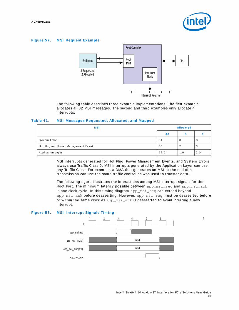
Figure 57. MSI Request Example
Endpoint
8 Requested2 Allocated
Root Complex
CPU
Interrupt Register
RootPort
InterruptBlock
The following table describes three example implementations. The first exampleallocates all 32 MSI messages. The second and third examples only allocate 4interrupts.
Table 41. MSI Messages Requested, Allocated, and Mapped
MSI Allocated
32 4 4
System Error 31 3 3
Hot Plug and Power Management Event 30 2 3
Application Layer 29:0 1:0 2:0
MSI interrupts generated for Hot Plug, Power Management Events, and System Errorsalways use Traffic Class 0. MSI interrupts generated by the Application Layer can useany Traffic Class. For example, a DMA that generates an MSI at the end of atransmission can use the same traffic control as was used to transfer data.
The following figure illustrates the interactions among MSI interrupt signals for theRoot Port. The minimum latency possible between app_msi_req and app_msi_ackis one clock cycle. In this timing diagram app_msi_req can extend beyondapp_msi_ack before deasserting. However, app_msi_req must be deasserted beforeor within the same clock as app_msi_ack is deasserted to avoid inferring a newinterrupt.
Figure 58. MSI Interrupt Signals Timing
clk
app_msi_req
app_msi_tc[2:0]
app_msi_num[4:0]
app_msi_ack
1 2 3 5 64 7
valid
valid
7 Interrupts
Intel® Stratix® 10 Avalon-ST Interface for PCIe Solutions User Guide85
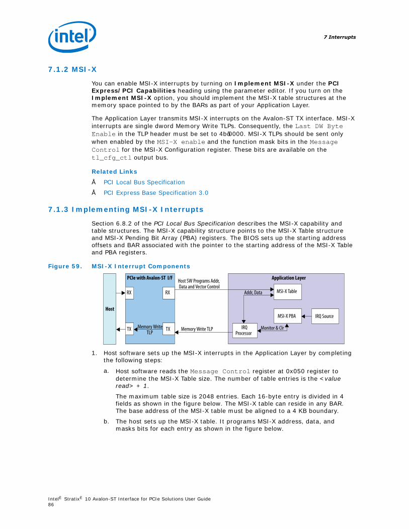
7.1.2 MSI-X
You can enable MSI-X interrupts by turning on Implement MSI-X under the PCIExpress/PCI Capabilities heading using the parameter editor. If you turn on theImplement MSI-X option, you should implement the MSI-X table structures at thememory space pointed to by the BARs as part of your Application Layer.
The Application Layer transmits MSI-X interrupts on the Avalon-ST TX interface. MSI-Xinterrupts are single dword Memory Write TLPs. Consequently, the Last DW ByteEnable in the TLP header must be set to 4b’0000. MSI-X TLPs should be sent onlywhen enabled by the MSI-X enable and the function mask bits in the MessageControl for the MSI-X Configuration register. These bits are available on thetl_cfg_ctl output bus.
Related Links
• PCI Local Bus Specification
• PCI Express Base Specification 3.0
7.1.3 Implementing MSI-X Interrupts
Section 6.8.2 of the PCI Local Bus Specification describes the MSI-X capability andtable structures. The MSI-X capability structure points to the MSI-X Table structureand MSI-X Pending Bit Array (PBA) registers. The BIOS sets up the starting addressoffsets and BAR associated with the pointer to the starting address of the MSI-X Tableand PBA registers.
Figure 59. MSI-X Interrupt Components
Host
RX
TX
RX
TX
PCIe with Avalon-ST I/F
MSI-X Table
IRQProcessor
MSI-X PBA IRQ Source
Application LayerHost SW Programs Addr,Data and Vector Control
Memory Write TLP
Memory Write TLP Monitor & Clr
Addr, Data
1. Host software sets up the MSI-X interrupts in the Application Layer by completingthe following steps:
a. Host software reads the Message Control register at 0x050 register todetermine the MSI-X Table size. The number of table entries is the <valueread> + 1.
The maximum table size is 2048 entries. Each 16-byte entry is divided in 4fields as shown in the figure below. The MSI-X table can reside in any BAR.The base address of the MSI-X table must be aligned to a 4 KB boundary.
b. The host sets up the MSI-X table. It programs MSI-X address, data, andmasks bits for each entry as shown in the figure below.
7 Interrupts
Intel® Stratix® 10 Avalon-ST Interface for PCIe Solutions User Guide86

Figure 60. Format of MSI-X Table
Vector ControlVector ControlVector Control
Vector Control
Message DataMessage DataMessage Data
Message Data
DWORD 3 DWORD 2Message Upper AddressMessage Upper AddressMessage Upper Address
Message Upper Address
DWORD 1Message AddressMessage AddressMessage Address
Message Address
DWORD 0 Host Byte AddressesEntry 0Entry 1Entry 2
Entry (N - 1)
BaseBase + 1 × 16Base + 2 × 16
Base + (N - 1) × 16
c. The host calculates the address of the <nth> entry using the followingformula:
nth_address = base address[BAR] + 16<n>
2. When Application Layer has an interrupt, it drives an interrupt request to the IRQSource module.
3. The IRQ Source sets appropriate bit in the MSI-X PBA table.
The PBA can use qword or dword accesses. For qword accesses, the IRQ Sourcecalculates the address of the <mth> bit using the following formulas:
qword address = <PBA base addr> + 8(floor(<m>/64))qword bit = <m> mod 64
Figure 61. MSI-X PBA Table
Pending Bits 0 through 63Pending Bits 64 through 127
Pending Bits (( N - 1) div 64) × 64 through N - 1
QWORD 0QWORD 1
QWORD (( N - 1) div 64)
BaseAddressPending Bit Array (PBA)
Base + 1 × 8
Base + ((N - 1) div 64) × 8
4. The IRQ Processor reads the entry in the MSI-X table.
a. If the interrupt is masked by the Vector_Control field of the MSI-X table,the interrupt remains in the pending state.
b. If the interrupt is not masked, IRQ Processor sends Memory Write Request tothe TX slave interface. It uses the address and data from the MSI-X table. IfMessage Upper Address = 0, the IRQ Processor creates a three-dwordheader. If the Message Upper Address > 0, it creates a 4-dword header.
5. The host interrupt service routine detects the TLP as an interrupt and services it.
Related Links
• Floor and ceiling functions
• PCI Local Bus Specification, Rev. 3.0
7 Interrupts
Intel® Stratix® 10 Avalon-ST Interface for PCIe Solutions User Guide87

7.1.4 Legacy Interrupts
The following figure illustrates interrupt timing for the legacy interface. In this figurethe assertion of app_int_sts instructs the Hard IP for PCI Express to send aAssert_INTx message TLP.
Figure 62. Legacy Interrupt Assertion
clk
app_int_sts
app_int_ack
The following figure illustrates the timing for deassertion of legacy interrupts. Theassertion of app_int_sts instructs the Hard IP for PCI Express to send aDeassert_INTx message.
Figure 63. Legacy Interrupt Deassertion
clk
app_int_sts
app_int_ack
7 Interrupts
Intel® Stratix® 10 Avalon-ST Interface for PCIe Solutions User Guide88
8 Registers
8.1 Configuration Space Registers
Table 42. Correspondence between Configuration Space Capability Structures and PCIeBase Specification Description
Byte Address Hard IP Configuration Space Register Corresponding Section in PCIe Specification
0x000:0x03C PCI Header Type 0 Configuration Registers Type 0 Configuration Space Header
0x040:0x04C Power Management PCI Power Management Capability Structure
0x050:0x05C MSI Capability Structure MSI Capability Structure, see also and PCI LocalBus Specification
0x060:0x06C Reserved N/A
0x070:0x0A8 PCI Express Capability Structure PCI Express Capability Structure
0x0B0:0x0B8 MSI-X Capability Structure MSI-X Capability Structure, see also and PCILocal Bus Specification
0x0BC:0x0FC Reserved N/A
0x100:0x134 Advanced Error Reporting (AER) Advanced Error Reporting Capability
0x138:188 Reserved N/A
0x188:0x1B4 Secondary PCI Express Extended CapabilityHeader
PCI Express Extended Capability
0x188:0xB7C Reserved N/A
0xB80:0xBAC Intel-Defined VSEC Capability Header Vendor-Specific Header (Header only)
0xC00 Optional Custom Extensions N/A
Summary of Configuration Space Register Fields
0x000 Device ID, Vendor ID Type 0 Configuration Space Header
0x004 Status, Command Type 0 Configuration Space Header
0x008 Class Code, Revision ID Type 0 Configuration Space Header
0x00C Header Type, Cache Line Size Type 0 Configuration Space Header
0x010 Base Address 0 Base Address Registers
0x014 Base Address 1 Base Address Registers
0x018 Base Address 2 Base Address Registers
0x01C Base Address 3 Base Address Registers
continued...
8 Registers
Intel Corporation. All rights reserved. Intel, the Intel logo, Altera, Arria, Cyclone, Enpirion, MAX, Nios, Quartusand Stratix words and logos are trademarks of Intel Corporation or its subsidiaries in the U.S. and/or othercountries. Intel warrants performance of its FPGA and semiconductor products to current specifications inaccordance with Intel's standard warranty, but reserves the right to make changes to any products and servicesat any time without notice. Intel assumes no responsibility or liability arising out of the application or use of anyinformation, product, or service described herein except as expressly agreed to in writing by Intel. Intelcustomers are advised to obtain the latest version of device specifications before relying on any publishedinformation and before placing orders for products or services.*Other names and brands may be claimed as the property of others.
ISO9001:2008Registered

Byte Address Hard IP Configuration Space Register Corresponding Section in PCIe Specification
0x020 Base Address 4 Base Address Registers
0x024 Base Address 5 Base Address Registers
0x028 Reserved N/A
0x02C Subsystem ID, Subsystem Vendor ID Type 0 Configuration Space Header
0x030 Reserved N/A
0x034 Capabilities Pointer Type 0 Configuration Space Header
0x038 Reserved N/A
0x03C Interrupt Pin, Interrupt Line Type 0 Configuration Space Header
0x040 PME_Support, D1, D2, etc. PCI Power Management Capability Structure
0x044 PME_en, PME_Status, etc. Power Management Status and Control Register
0x050 MSI-Message Control, Next Cap Ptr, Capability ID MSI and MSI-X Capability Structures
0x054 Message Address MSI and MSI-X Capability Structures
0x058 Message Upper Address MSI and MSI-X Capability Structures
0x05C Reserved Message Data MSI and MSI-X Capability Structures
0x0B0 MSI-X Message Control Next Cap Ptr CapabilityID
MSI and MSI-X Capability Structures
0x0B4 MSI-X Table Offset BIR MSI and MSI-X Capability Structures
0x0B8 Pending Bit Array (PBA) Offset BIR MSI and MSI-X Capability Structures
0x100 PCI Express Enhanced Capability Header Advanced Error Reporting Enhanced CapabilityHeader
0x104 Uncorrectable Error Status Register Uncorrectable Error Status Register
0x108 Uncorrectable Error Mask Register Uncorrectable Error Mask Register
0x10C Uncorrectable Error Mask Register Uncorrectable Error Severity Register
0x110 Correctable Error Status Register Correctable Error Status Register
0x114 Correctable Error Mask Register Correctable Error Mask Register
0x118 Advanced Error Capabilities and Control Register Advanced Error Capabilities and Control Register
0x11C Header Log Register Header Log Register
0x12C Root Error Command Root Error Command Register
0x130 Root Error Status Root Error Status Register
0x134 Error Source Identification Register CorrectableError Source ID Register
Error Source Identification Register
0x188 Next Capability Offset, PCI Express ExtendedCapability ID
Secondary PCI Express Extended Capability
0x18C Enable SKP OS, Link Equalization Req, PerformEqualization
Link Control 3 Register
0x190 Lane Error Status Register Lane Error Status Register
0x194 Lane Equalization Control Register Lane Equalization Control Register
0xB80 VSEC Capability Header Vendor-Specific Extended Capability Header
continued...
8 Registers
Intel® Stratix® 10 Avalon-ST Interface for PCIe Solutions User Guide90

Byte Address Hard IP Configuration Space Register Corresponding Section in PCIe Specification
0xB84 VSEC Length, Revision, ID Vendor-Specific Header
0xB88 Intel Marker
Intel-Specific Registers
0xB8C JTAG Silicon ID DW0
0xB90 JTAG Silicon ID DW1
0xB94 JTAG Silicon ID DW2
0xB98 JTAG Silicon ID DW3
0xB9C User Device and Board Type ID
0xBA0::BAC Reserved
0xBB0 General Purpose Control and Status Register
0xBB4 Uncorrectable Internal Error Status Register
0xBB8 Uncorrectable Internal Error Mask Register
0xBBC Correctable Error Status Register
0xBC0 Correctable Error Mask Register
0xBC4:BD8 Reserved N/A
0xC00 Optional Custom Extensions N/A
Related Links
• PCI Express Base Specification 3.0
• PCI Local Bus Specification
8.1.1 Type 0 Configuration Space Registers
Endpoints store configuration data in the Type 0 Configuration Space. TheCorrespondence between Configuration Space Registers and the PCIe Specificationlists the appropriate section of the PCI Express Base Specification that describes theseregisters.
Figure 64. Configuration Space Registers Address Map
PCI Header Type 0PCI Power Management
MSIPCI Express
MSI-XAER
VSECCustom Extensions
RequiredRequiredOptionalRequiredOptionalRequired
RequiredOptional
0x000x400x500x700xB0
0x100
0xB800xC00
End Point Capability Structure Required/Optional Starting Byte Offset
Secondary PCIe Required 0x188
8 Registers
Intel® Stratix® 10 Avalon-ST Interface for PCIe Solutions User Guide91

Figure 65. Type 0 Configuration Space Registers - Byte Address Offsets and Layout
0x0000x0040x0080x00C0x0100x0140x0180x01C0x0200x0240x0280x02C0x0300x0340x0380x03C
Device ID Vendor IDStatus Command
Class Code Revision ID
0x00 Header Type 0x00 Cache Line SizeBAR RegistersBAR RegistersBAR RegistersBAR RegistersBAR RegistersBAR Registers
ReservedSubsystem Device ID Subsystem Vendor ID
ReservedReserved
Reserved
Capabilities Pointer
0x00 Interrupt Pin Interrupt Line
31 24 23 16 15 8 7 0
Related Links
PCI Express Base Specification 3.0
8.1.2 PCI Express Capability Structures
The layout of the most basic Capability Structures are provided below. Refer to the PCIExpress Base Specification for more information about these registers.
Figure 66. Power Management Capability Structure - Byte Address Offsets and Layout
0x040
0x04C
Capabilities Register Next Cap Ptr
Data
31 24 23 16 15 8 7 0Capability ID
Power Management Status and ControlPM Control/StatusBridge Extensions
8 Registers
Intel® Stratix® 10 Avalon-ST Interface for PCIe Solutions User Guide92
Figure 67. MSI Capability Structure
0x050
0x0540x058
Message ControlConfiguration MSI Control Status
Register Field DescriptionsNext Cap Ptr
Message AddressMessage Upper Address
Reserved Message Data
31 24 23 16 15 8 7 0
0x05C
Capability ID
Figure 68. PCI Express Capability Structure - Byte Address Offsets and LayoutIn the following table showing the PCI Express Capability Structure, registers that arenot applicable to a device are reserved.
0x070
0x0740x0780x07C0x0800x0840x0880x08C0x0900x0940x0980x09C0x0A00x0A4
0x0A8
PCI Express Capabilities Register Next Cap Pointer
Device CapabilitiesDevice Status Device Control
Slot Capabilities
Root StatusDevice Compatibilities 2
Link Capabilities 2Link Status 2 Link Control 2
Slot Capabilities 2
Slot Status 2 Slot Control 2
31 24 23 16 15 8 7 0PCI Express
Capabilities ID
Link CapabilitiesLink Status Link Control
Slot Status Slot Control
Device Status 2 Device Control 2
Root Capabilities Root Control
8 Registers
Intel® Stratix® 10 Avalon-ST Interface for PCIe Solutions User Guide93

Figure 69. MSI-X Capability Structure
0x0B0
0x0B4
0x0B8
Message Control Next Cap Ptr
MSI-X Table Offset
MSI-X Pending Bit Array (PBA) Offset
31 24 23 16 15 8 7 0Capability ID
3 2
MSI-XTable BAR
IndicatorMSI-X
PendingBit Array
- BARIndicator
Figure 70. PCI Express AER Extended Capability Structure
Byte Offs et 31:24 23:16 15:8 7:0
0x100
0x104 Uncorrectable Error Status Register
PCI Express Enhanced Capability Register
Uncorrectable Error Severity Register
Uncorrectable Error Mask Register0x108
0x10C
0x110
0x114
0x118
0x11C
0x12C
0x130
0x134
Correctable Error Status Register
Correctable Error Mask Register
Advanced Error Capabilities and Control Register
Header Log Register
Root Error Command Register
Root Error Status Register
Error Source Identification Register Correctable Error Source Identification Register
Related Links
• PCI Express Base Specification 3.0
• PCI Local Bus Specification
8.1.3 JTAG Silicon ID
This read only register returns the JTAG Silicon ID. The Intel Programming softwareuses this JTAG ID to make ensure that it is programming the SRAM Object File(*.sof) .
Table 43. JTAG Silicon ID - 0xB8C-0xB98
Bits Register Description Default Value3
Access
[127:96 JTAG Silicon ID DW3 Unique ID RO
[95:64] JTAG Silicon ID DW2 Unique ID RO
[63:32] JTAG Silicon ID DW1 Unique ID RO
[31:0] JTAG Silicon ID DW0 Unique ID RO
3 Because the Silicon ID is a unique value, it does not have a global default value.
8 Registers
Intel® Stratix® 10 Avalon-ST Interface for PCIe Solutions User Guide94

8.1.4 Intel Defined VSEC Capability Header
The figure below shows the address map and layout of the Intel defined VSECCapability.
Figure 71. Vendor-Specific Extended Capability Address Map and Register Layout
31 24 23 16 15 8 7 0Next Cap Offset
VSEC LengthVersion
VSEC RevisionPCI Express Extended Capability ID
VSEC ID00h04h08h0Ch10h14h18h1Ch20h24h28h2Ch30h34h38h3Ch40h44h48h4Ch50h54h58h
Intel MarkerJTAG Silicon ID DW0JTAG Silicon ID DW1JTAG Silicon ID DW2JTAG Silicon ID DW3
Reserved User Configurable Device/Board IDReservedReservedReservedReserved
General-Purpose Control and StatusUncorrectable Internal Error Status RegisterUncorrectable Internal Error Mask RegisterCorrectable Internal Error Status RegisterCorrectable Internal Error Mask Register
ReservedReservedReservedReservedReservedReserved
Table 44. Altera-Defined VSEC Capability Header - 0xB80
Bits Register Description Default Value Access
[31:20] Next Capability Pointer: Value is the starting address of the next CapabilityStructure implemented. Otherwise, NULL.
Variable RO
[19:16] Version. PCIe specification defined value for VSEC version. 1 RO
[15:0] PCI Express Extended Capability ID. PCIe specification defined value forVSEC Capability ID.
0x000B RO
8 Registers
Intel® Stratix® 10 Avalon-ST Interface for PCIe Solutions User Guide95

8.1.5 Intel Defined Vendor Specific Header
Table 45. Intel defined Vendor Specific Header - 0xB84
Bits Register Description Default Value Access
[31:20] VSEC Length. Total length of this structure in bytes. 0x5C RO
[19:16] VSEC. User configurable VSEC revision. Not available RO
[15:0] VSEC ID. User configurable VSEC ID. You should change this ID to yourVendor ID.
0x1172 RO
8.1.6 Intel Marker
Table 46. Intel Marker - 0xB88
Bits Register Description Default Value Access
[31:0] Intel Marker - An additional marker for standard Intel programmingsoftware to be able to verify that this is the right structure.
0x41721172 RO
8.1.7 User Device and Board Type ID
Table 47. User Device and Board Type ID - 0xB9C
Bits Register Description Default Value Access
[15:0] Allows you to specify ID of the .sof file to be loaded.From
configurationbits
RO
8.1.8 General Purpose Control and Status Register
This register provides up to eight I/O pins for Application Layer control and statusrequirements. This feature supports Partial Reconfiguration of the FPGA fabric. PartialReconfiguration only requires one input and one output pin. The other seven I/Osmake this interface extensible.
Table 48. General Purpose Control and Status Register - 0xBB0
Bits Register Description Default Value Access
[31:16] Reserved. N/A RO
[15:8] General Purpose Status. The Application Layer can read status bits. 0 RO
[7:0] General Purpose Control. The Application Layer can write control bits. 0 RW
8.1.9 Uncorrectable Internal Error Status Register
This register reports the status of the internally checked errors that areuncorrectable.When these specific errors are enabled by the UncorrectableInternal Error Mask register, they are forwarded as Correctable Internal Errors.This register is for debug only. Only use this register to observe behavior, not to drivelogic custom logic.
8 Registers
Intel® Stratix® 10 Avalon-ST Interface for PCIe Solutions User Guide96
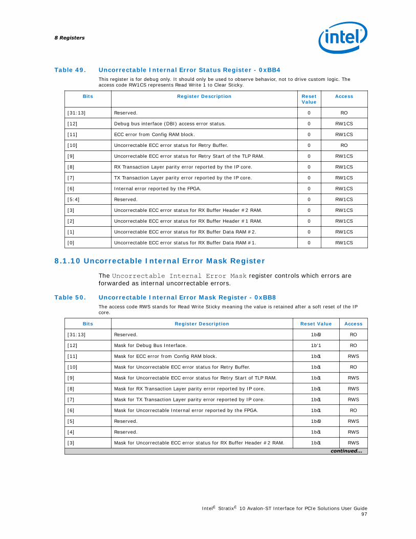
Table 49. Uncorrectable Internal Error Status Register - 0xBB4This register is for debug only. It should only be used to observe behavior, not to drive custom logic. Theaccess code RW1CS represents Read Write 1 to Clear Sticky.
Bits Register Description ResetValue
Access
[31:13] Reserved. 0 RO
[12] Debug bus interface (DBI) access error status. 0 RW1CS
[11] ECC error from Config RAM block. 0 RW1CS
[10] Uncorrectable ECC error status for Retry Buffer. 0 RO
[9] Uncorrectable ECC error status for Retry Start of the TLP RAM. 0 RW1CS
[8] RX Transaction Layer parity error reported by the IP core. 0 RW1CS
[7] TX Transaction Layer parity error reported by the IP core. 0 RW1CS
[6] Internal error reported by the FPGA. 0 RW1CS
[5:4] Reserved. 0 RW1CS
[3] Uncorrectable ECC error status for RX Buffer Header #2 RAM. 0 RW1CS
[2] Uncorrectable ECC error status for RX Buffer Header #1 RAM. 0 RW1CS
[1] Uncorrectable ECC error status for RX Buffer Data RAM #2. 0 RW1CS
[0] Uncorrectable ECC error status for RX Buffer Data RAM #1. 0 RW1CS
8.1.10 Uncorrectable Internal Error Mask Register
The Uncorrectable Internal Error Mask register controls which errors areforwarded as internal uncorrectable errors.
Table 50. Uncorrectable Internal Error Mask Register - 0xBB8The access code RWS stands for Read Write Sticky meaning the value is retained after a soft reset of the IPcore.
Bits Register Description Reset Value Access
[31:13] Reserved. 1b’0 RO
[12] Mask for Debug Bus Interface. 1b'1 RO
[11] Mask for ECC error from Config RAM block. 1b’1 RWS
[10] Mask for Uncorrectable ECC error status for Retry Buffer. 1b’1 RO
[9] Mask for Uncorrectable ECC error status for Retry Start of TLP RAM. 1b’1 RWS
[8] Mask for RX Transaction Layer parity error reported by IP core. 1b’1 RWS
[7] Mask for TX Transaction Layer parity error reported by IP core. 1b’1 RWS
[6] Mask for Uncorrectable Internal error reported by the FPGA. 1b’1 RO
[5] Reserved. 1b’0 RWS
[4] Reserved. 1b’1 RWS
[3] Mask for Uncorrectable ECC error status for RX Buffer Header #2 RAM. 1b’1 RWS
continued...
8 Registers
Intel® Stratix® 10 Avalon-ST Interface for PCIe Solutions User Guide97

Bits Register Description Reset Value Access
[2] Mask for Uncorrectable ECC error status for RX Buffer Header #1 RAM. 1b’1 RWS
[1] Mask for Uncorrectable ECC error status for RX Buffer Data RAM #2. 1b’1 RWS
[0] Mask for Uncorrectable ECC error status for RX Buffer Data RAM #1. 1b’1 RWS
8.1.11 Correctable Internal Error Status Register
Table 51. Correctable Internal Error Status Register - 0xBBCThe Correctable Internal Error Status register reports the status of the internally checked errors thatare correctable. When these specific errors are enabled by the Correctable Internal Error Maskregister, they are forwarded as Correctable Internal Errors. This register is for debug only. Only use thisregister to observe behavior, not to drive logic custom logic.
Bits Register Description ResetValue
Access
[31:12] Reserved. 0 RO
[11] Correctable ECC error status for Config RAM. 0 RW1CS
[10] Correctable ECC error status for Retry Buffer. 0 RW1CS
[9] Correctable ECC error status for Retry Start of TLP RAM. 0 RW1CS
[8] Reserved. 0 RO
[7] Reserved. 0 RO
[6] Internal Error reported by FPGA. 0 RW1CS
[5] Reserved 0 RO
[4] PHY Gen3 SKP Error occurred. Gen3 data pattern contains SKP pattern(8'b10101010) is misinterpreted as a SKP OS and causing erroneousblock realignment in the PHY.
0 RW1CS
[3] Correctable ECC error status for RX Buffer Header RAM #2. 0 RW1CS
[2] Correctable ECC error status for RX Buffer Header RAM #1. 0 RW1CS
[1] Correctable ECC error status for RX Buffer Data RAM #2. 0 RW1CS
[0] Correctable ECC error status for RX Buffer Data RAM #1. 0 RW1CS
8.1.12 Correctable Internal Error Mask Register
Table 52. Correctable Internal Error Status Register - 0xBBCThe Correctable Internal Error Status register controls which errors are forwarded as InternalCorrectable Errors.
Bits Register Description ResetValue
Access
[31:12] Reserved. 0 RO
[11] Mask for correctable ECC error status for Config RAM. 0 RWS
[10] Mask for correctable ECC error status for Retry Buffer. 1 RWS
[9] Mask for correctable ECC error status for Retry Start of TLP RAM. 1 RWS
continued...
8 Registers
Intel® Stratix® 10 Avalon-ST Interface for PCIe Solutions User Guide98

Bits Register Description ResetValue
Access
[8] Reserved. 0 RO
[7] Reserved. 0 RO
[6] Mask for internal Error reported by FPGA. 0 RWS
[5] Reserved 0 RO
[4] Mask for PHY Gen3 SKP Error. 1 RWS
[3] Mask for correctable ECC error status for RX Buffer Header RAM #2. 1 RWS
[2] Mask for correctable ECC error status for RX Buffer Header RAM #1. 1 RWS
[1] Mask for correctable ECC error status for RX Buffer Data RAM #. 1 RWS
[0] Mask for correctable ECC error status for RX Buffer Data RAM #1. 1 RWS
8.2 Avalon-MM DMA Bridge Registers
8.2.1 PCI Express Avalon-MM Bridge Register Address Map
The registers included in the Avalon-MM bridge map to a 32 KB address space. Readsto undefined addresses have unpredictable results.
Table 53. Stratix 10 PCIe Avalon-MM Bridge Register Map
Address Range Registers
0x0040 PCIe Interrupt Status Register
0x0050 PCIe Interrupt Enable Register
0x0800-0x081F PCIe to Avalon Mailbox Registers
0x0900-0x091F Avalon to PCIe Mailbox Registers
0x1000-0x1FFF Address Translation Table for the Bursting Avalon-MM Slave
0x3060 Avalon-MM Interrupt Status Register
0x3070 Avalon Interrupt Enable Register
0x3A00–0x3A1F Avalon-MM to PCIe Mailbox Registers
0x3B00–0x3B1F PCIe to Avalon-MM Mailbox Registers
0x3C00-0x3C1F PCIe Configuration Information Registers
8.2.1.1 Avalon-MM to PCI Express Interrupt Status Registers
These registers contain the status of various signals in the PCI Express Avalon-MMbridge logic. These registers allow MSI or legacy interrupts to be asserted whenenabled.
Only Root Complexes should access these registers; however, hardware does notprevent other Avalon-MM masters from accessing them.
8 Registers
Intel® Stratix® 10 Avalon-ST Interface for PCIe Solutions User Guide99

Table 54. Avalon-MM to PCI Express Interrupt Status Register, 0x0040
Bit Name Access Description
[31:24] Reserved N/A N/A
[23] A2P_MAILBOX_INT7 RW1C 1 when the A2P_MAILBOX7 is written to
[22] A2P_MAILBOX_INT6 RW1C 1 when the A2P_MAILBOX6 is written to
[21] A2P_MAILBOX_INT5 RW1C 1 when the A2P_MAILBOX5 is written to
[20] A2P_MAILBOX_INT4 RW1C 1 when the A2P_MAILBOX4 is written to
[19] A2P_MAILBOX_INT3 RW1C 1 when the A2P_MAILBOX3 is written to
[18] A2P_MAILBOX_INT2 RW1C 1 when the A2P_MAILBOX2 is written to
[17] A2P_MAILBOX_INT1 RW1C 1 when the A2P_MAILBOX1 is written to
[16] A2P_MAILBOX_INT0 RW1C 1 when the A2P_MAILBOX0 is written to
[15:0] User Interrupts RW1C If the Application implements interrupts usingrxm_irq[15:0], this register records interruptstatus. Set to 1'b1 on the rising edge of thecorresponding bit of rxm_irq[15:0]. .
8.2.1.2 Avalon-MM to PCI Express Interrupt Enable Registers
The interrupt enable registers enable either MSI or legacy interrupts.
A PCI Express interrupt can be asserted for any of the conditions registered in theAvalon-MM to PCI Express Interrupt Status register by setting thecorresponding bits in the Avalon-MM to PCI Express Interrupt Enable register.
Table 55. Avalon-MM to PCI Express Interrupt Enable Register, 0x0050
Bits Name Access Description
[31:0] 1-for-1 enable mapping for the bits in thePCIe Interrupt Status register
RW When set to 1, indicates the setting of theassociated bit in the PCIe InterruptStatus register causes the legacy PCIe orMSI interrupt to be generated.
Table 56. Avalon-MM Interrupt Vector Register - 0x0060
Bits Name Access Description
[31:16] Reserved N/A N/A
[15:0] AVL_IRQ_Vector RO Stores the interrupt vector of the systeminterconnect fabric. When the host receives aninterrupt, it should read this register todetermine the servicing priority.
8.2.1.3 PCI Express Mailbox Registers
The PCI Express Root Complex typically requires write access to a set of PCIExpress to Avalon-MM Mailbox registers and read-only access to a set ofAvalon-MM to PCI Express mailbox registers. Eight mailbox registers areavailable.
8 Registers
Intel® Stratix® 10 Avalon-ST Interface for PCIe Solutions User Guide100

The PCI Express to Avalon MM Mailbox registers are writable at the addressesshown in the following table. Writing to one of these registers causes thecorresponding bit in the Avalon-MM Interrupt Status register to be set to a one.
Table 57. PCI Express to Avalon-MM Mailbox Registers, 0x0800–0x081F
Address Name Access Description
0x0800 P2A_MAILBOX0 RW PCI Express-to-Avalon-MM Mailbox 0
0x0804 P2A_MAILBOX1 RW PCI Express-to-Avalon-MM Mailbox 1
0x0808 P2A_MAILBOX2 RW PCI Express-to-Avalon-MM Mailbox 2
0x080C P2A_MAILBOX3 RW PCI Express-to-Avalon-MM Mailbox 3
0x0810 P2A_MAILBOX4 RW PCI Express-to-Avalon-MM Mailbox 4
0x0814 P2A_MAILBOX5 RW PCI Express-to-Avalon-MM Mailbox 5
0x0818 P2A_MAILBOX6 RW PCI Express-to-Avalon-MM Mailbox 6
0x081C P2A_MAILBOX7 RW PCI Express-to-Avalon-MM Mailbox 7
The Avalon-MM to PCI Express Mailbox registers are read at the addressesshown in the following table. The PCI Express Root Complex should use theseaddresses to read the mailbox information after being signaled by the correspondingbits in the Avalon-MM to PCI Express Interrupt Status register.
Table 58. Avalon-MM to PCI Express Mailbox Registers, 0x0900–0x091F
Address Name Access Description
0x0900 A2P_MAILBOX0 RO Avalon-MM-to-PCI Express Mailbox 0
0x0904 A2P_MAILBOX1 RO Avalon-MM-to-PCI Express Mailbox 1
0x0908 A2P_MAILBOX2 RO Avalon-MM-to-PCI Express Mailbox 2
0x090C A2P_MAILBOX3 RO Avalon-MM-to-PCI Express Mailbox 3
0x0910 A2P_MAILBOX4 RO Avalon-MM-to-PCI Express Mailbox 4
0x0914 A2P_MAILBOX5 RO Avalon-MM-to-PCI Express Mailbox 5
0x0918 A2P_MAILBOX6 RO Avalon-MM-to-PCI Express Mailbox 6
0x091C A2P_MAILBOX7 RO Avalon-MM-to-PCI Express Mailbox 7
8.2.1.4 Address Mapping for High-Performance Avalon-MM 32-Bit Slave Modules
Address mapping for 32-bit Avalon-MM slave devices allows system software to specifynon-contiguous address pages in the PCI Express address domain. All highperformance 32-bit Avalon-MM slave devices are mapped to the 64-bit PCI Expressaddress space. The Avalon-MM Settings tab of the component GUI allows you toselect the number and size of address mapping pages. Up to 10 address mappingpages are supported. The minimum page size is 4 KB. The maximum page size is 4GB.
When you enable address mapping, the slave address bus width is just large enoughto fit the required address mapping pages. When address mapping is disabled, theAvalon-MM slave address bus is set to 64 bits. The Avalon-MM addresses are used as-is in the resulting PCIe TLPs.
8 Registers
Intel® Stratix® 10 Avalon-ST Interface for PCIe Solutions User Guide101

When address mapping is enabled, bursts on the Avalon-MM slave interfaces must notcross page boundaries. This restriction means:
(address + 32 * burst count) <= (page base address + page size )
Address Mapping TableThe address mapping table is accessible through the Control and Status registers.Each entry in the address mapping table is 64 bits (8 bytes) wide and is composed oftwo successive registers. The even address registers holds bits [31:0]. The oddaddress registers holds bits [63:32]. The lower-order address bits are passed throughto the PCIe TLPs unchanged and are ignored in the address mapping table. Thenumber of LSBs that are passed through defines the size of the page and is set atconfiguration time. If bits [63:32] of the resulting PCIe address are zero, TLPs with32-bit wide addresses are created as required by the PCI Express standard.
Table 59. Avalon-MM-to-PCI Express Address Translation Table, 0x1000–0x1FFF
Address Name Access Description
0x1000 A2P_ADDR_MAP_LO0
RW Lower bits of Avalon-MM-to-PCI Express address map entry 0.
0x1004 A2P_ADDR_MAP_HI0
RW Upper bits of Avalon-MM-to-PCI Express address map entry 0.
0x1008 A2P_ADDR_MAP_LO1
RW Lower bits of Avalon-MM-to-PCI Express address map entry 0.This entry is only implemented if the number of address translationtable entries is greater than 1.
0x100C A2P_ADDR_MAP_HI1
RW Upper bits of Avalon-MM-to-PCI Express address map entry 1.This entry is only implemented if the number of address translationtable entries is greater than 1.
8.2.1.5 PCI Express to Avalon-MM Interrupt Status and Enable Registers forEndpoints
These registers record the status of various signals in the PCI Express Avalon-MMbridge logic. They allow Avalon-MM interrupts to be asserted when enabled. Aprocessor local to the interconnect fabric that processes the Avalon-MM interrupts canaccess these registers.
Note: These registers must not be accessed by the PCI Express Avalon-MM bridge masterports. However, nothing in the hardware prevents a PCI Express Avalon-MM bridgemaster port from accessing these registers.
The following table describes the Interrupt Status register for Endpoints. It records thestatus of all conditions that can cause an Avalon-MM interrupt to be asserted.
Table 60. PCI Express to Avalon-MM Interrupt Status Register for Endpoints, 0x3060
Bits Name Access Description
[31:24] Reserved N/A Reserved
[23] P2A_MAILBOX_INT7 RW1C Set to a 1 when the P2A_MAILBOX7 is writtento.
[22] P2A_MAILBOX_INT6 RW1C Set to a 1 when the P2A_MAILBOX6
continued...
8 Registers
Intel® Stratix® 10 Avalon-ST Interface for PCIe Solutions User Guide102

Bits Name Access Description
[21] P2A_MAILBOX_INT5 RW1C Set to a 1 when the P2A_MAILBOX5
[20] P2A_MAILBOX_INT4 RW1C Set to a 1 when the P2A_MAILBOX4
[19] P2A_MAILBOX_INT3 RW1C Set to a 1 when the P2A_MAILBOX3
[18] P2A_MAILBOX_INT2 RW1C Set to a 1 when the P2A_MAILBOX2
[17] P2A_MAILBOX_INT1 RW1C Set to a 1 when the P2A_MAILBOX1
[16] P2A_MAILBOX_INT0 RW1C Set to a 1 when the P2A_MAILBOX0
[15:0] Reserved N/A Reserved
An Avalon-MM interrupt can be asserted for any of the conditions noted in theAvalon-MM Interrupt Status register by setting the corresponding bits in thePCI Express to Avalon-MM Interrupt Enable register.
PCI Express interrupts can also be enabled for all of the error conditions described.However, it is likely that only one of the Avalon-MM or PCI Express interrupts can beenabled for any given bit. Typically, a single process in either the PCI Express orAvalon-MM domain handles the condition reported by the interrupt.
Table 61. INTX Interrupt Enable Register for Endpoints, 0x3070
Bits Name Access Description
[31:0] 1-for1 enable mapping for the bits in theAvalon-MM Interrupt Status register.
RW When set to 1, indicates the setting of theassociated bit in the Avalon-MM InterruptStatus register will cause the Avalon-MMinterrupt signal, cra_irq_o, to be asserted.
8.2.1.6 Avalon-MM Mailbox Registers
A processor local to the interconnect fabric typically requires write access to a set ofAvalon-MM to PCI Express Mailbox registers and read-only access to a set ofPCI Express to Avalon-MM Mailbox registers. Eight mailbox registers areavailable.
The Avalon-MM to PCI Express Mailbox registers are writable at the addressesshown in the following table. When the Avalon-MM processor writes to one of theseregisters the corresponding bit in the Avalon-MM to PCI Express InterruptStatus register is set to 1.
Table 62. Avalon-MM to PCI Express Mailbox Registers, 0x3A00–0x3A1F
Address Name Access Description
0x3A00 A2P_MAILBOX0 RW Avalon-MM-to-PCI Express mailbox 0
0x3A04 A2P_MAILBOX1 RW Avalon-MM-to-PCI Express mailbox 1
0x3A08 A2P _MAILBOX2 RW Avalon-MM-to-PCI Express mailbox 2
0x3A0C A2P _MAILBOX3 RW Avalon-MM-to-PCI Express mailbox 3
0x3A10 A2P _MAILBOX4 RW Avalon-MM-to-PCI Express mailbox 4
continued...
8 Registers
Intel® Stratix® 10 Avalon-ST Interface for PCIe Solutions User Guide103
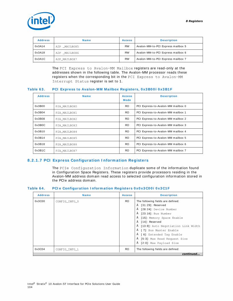
Address Name Access Description
0x3A14 A2P _MAILBOX5 RW Avalon-MM-to-PCI Express mailbox 5
0x3A18 A2P _MAILBOX6 RW Avalon-MM-to-PCI Express mailbox 6
0x3A1C A2P_MAILBOX7 RW Avalon-MM-to-PCI Express mailbox 7
The PCI Express to Avalon-MM Mailbox registers are read-only at theaddresses shown in the following table. The Avalon-MM processor reads theseregisters when the corresponding bit in the PCI Express to Avalon-MMInterrupt Status register is set to 1.
Table 63. PCI Express to Avalon-MM Mailbox Registers, 0x3B00–0x3B1F
Address Name AccessMode
Description
0x3B00 P2A_MAILBOX0 RO PCI Express-to-Avalon-MM mailbox 0
0x3B04 P2A_MAILBOX1 RO PCI Express-to-Avalon-MM mailbox 1
0x3B08 P2A_MAILBOX2 RO PCI Express-to-Avalon-MM mailbox 2
0x3B0C P2A_MAILBOX3 RO PCI Express-to-Avalon-MM mailbox 3
0x3B10 P2A_MAILBOX4 RO PCI Express-to-Avalon-MM mailbox 4
0x3B14 P2A_MAILBOX5 RO PCI Express-to-Avalon-MM mailbox 5
0x3B18 P2A_MAILBOX6 RO PCI Express-to-Avalon-MM mailbox 6
0x3B1C P2A_MAILBOX7 RO PCI Express-to-Avalon-MM mailbox 7
8.2.1.7 PCI Express Configuration Information Registers
The PCIe Configuration Information duplicate some of the information foundin Configuration Space Registers. These registers provide processors residing in theAvalon-MM address domain read access to selected configuration information stored inthe PCIe address domain.
Table 64. PCIe Configuration Information Registers 0x0x3C00–0x3C1F
Address Name Access Description
0x3C00 CONFIG_INFO_0 RO The following fields are defined:• [31:29]: Reserved• [28:24]: Device Number• [23:16]: Bus Number• [15]: Memory Space Enable• [14]: Reserved• [13:8]: Auto Negotiation Link Width• [ 7]: Bus Master Enable• [ 6]: Extended Tag Enable• [5:3]: Max Read Request Size• [2:0]: Max Payload Size
0x3C04 CONFIG_INFO_1 RO The following fields are defined:
continued...
8 Registers
Intel® Stratix® 10 Avalon-ST Interface for PCIe Solutions User Guide104

Address Name Access Description
• [31:29]: Reserved• [28:24] : AER Interrupt Msg No• [23:18]: Auto Negotiation Link
Width
• [17]: cfg_pm_no_soft_rs• [16]: Read Cpl Boundary (RBC)
Control
• [15:13]: Reserved• [12:8]: PCIe Capability Interrupt
Msg No
• [7:5]: Reserved• [4]: System Power Control• [3:2]: System Attention Indicator
Control
• [1:0]: System Power IndicatorControl
0x3C08 CONFIG_INFO_2 RO The following fields are defined:• [31:30]: Reserved• [29:24]: Index of Start VF[6:0]• [23:16]: Number of VFs• [15:12]: Auto Negotiation Link
Speed
• [11:8] ATS STU[4:1]• [7]: ATS STU[0]• [6]: ATS Cache Enable• [5]: ARI forward enable• [4]: Atomic request enable• [3:2]: TPH ST mode[1:0]• [1]: TPH enable[0]• [0]: VF enable
0x3C0C CONFIG_INFO_3 RO MSI Address Lower
0x3C10 CONFIG_INFO_4 RO MSI Address Upper
0x3C14 CONFIG_INFO_5 RO MSI Mask
0x3C18 CONFIG_INFO_6 RO The following fields are defined:• [31:16] : MSI Data• [15:7]: Reserved• [6]: MSI-X Func Mask• [5]: MSI-X Enable• [4:2]: Multiple MSI Enable• [ 1]: 64-bit MSI• [ 0]: MSI Enable
0x3C1C CONFIG_INFO_7 RO The following fields are defined:• [31:10]: Reserved• [9:6]: Auto Negotiation Link Speed• [5:0]: Auto Negotiation Link Width
8 Registers
Intel® Stratix® 10 Avalon-ST Interface for PCIe Solutions User Guide105

9 Testbench and Design ExampleThis chapter introduces the Endpoint design example including a testbench, BFM, anda test driver module. You can create this design example for using design flowsdescribed in Example Design for the Avalon-ST Stratix 10 Hard IP for PCI Express IPCore.
This testbench simulates up to x8 variants. It supports x16 variants by down-trainingto x8. To simulate all lanes of a x16 variant, you can create a simulation model inQsys to use in an Avery testbench. For more information refer to AN-811: Using theAvery BFM for PCI Express Gen3x16 Simulation on Intel Stratix 10 Devices.
When configured as an Endpoint variation, the testbench instantiates a designexample and a Root Port BFM, which provides the following functions:
• A configuration routine that sets up all the basic configuration registers in theEndpoint. This configuration allows the Endpoint application to be the target andinitiator of PCI Express transactions.
• A Verilog HDL procedure interface to initiate PCI Express transactions to theEndpoint.
The testbench uses a test driver module, altpcietb_bfm_driver_chaining toexercise the chaining DMA of the design example. The test driver module displaysinformation from the Endpoint Configuration Space registers, so that you can correlateto the parameters you specified using the parameter editor.
This testbench simulates a single Endpoint DUT.
The testbench uses a test driver module, altpcietb_bfm_driver_rp, to exercise thetarget memory and DMA channel in the Endpoint BFM. The test driver module displaysinformation from the Root Port Configuration Space registers, so that you cancorrelate to the parameters you specified using the parameter editor. The Endpointmodel consists of an Endpoint variation combined with the chaining DMA applicationdescribed above.
Note: The Intel testbench and Root Port BFM provide a simple method to do basic testing ofthe Application Layer logic that interfaces to the variation. This BFM allows you tocreate and run simple task stimuli with configurable parameters to exercise basicfunctionality of the Intel example design. The testbench and Root Port BFM are notintended to be a substitute for a full verification environment. Corner cases andcertain traffic profile stimuli are not covered. Refer to the items listed below for furtherdetails. To ensure the best verification coverage possible, Intel suggests strongly thatyou obtain commercially available PCI Express verification IP and tools, or do yourown extensive hardware testing or both.
9 Testbench and Design Example
Intel Corporation. All rights reserved. Intel, the Intel logo, Altera, Arria, Cyclone, Enpirion, MAX, Nios, Quartusand Stratix words and logos are trademarks of Intel Corporation or its subsidiaries in the U.S. and/or othercountries. Intel warrants performance of its FPGA and semiconductor products to current specifications inaccordance with Intel's standard warranty, but reserves the right to make changes to any products and servicesat any time without notice. Intel assumes no responsibility or liability arising out of the application or use of anyinformation, product, or service described herein except as expressly agreed to in writing by Intel. Intelcustomers are advised to obtain the latest version of device specifications before relying on any publishedinformation and before placing orders for products or services.*Other names and brands may be claimed as the property of others.
ISO9001:2008Registered

Your Application Layer design may need to handle at least the following scenarios thatare not possible to create with the Intel testbench and the Root Port BFM:
• It is unable to generate or receive Vendor Defined Messages. Some systemsgenerate Vendor Defined Messages and the Application Layer must be designed toprocess them. The Hard IP block passes these messages on to the ApplicationLayer which, in most cases should ignore them.
• It can only handle received read requests that are less than or equal to thecurrently set Maximum payload size option specified under PCI Express/PCICapabilities heading under the Device tab using the parameter editor. Manysystems are capable of handling larger read requests that are then returned inmultiple completions.
• It always returns a single completion for every read request. Some systems splitcompletions on every 64-byte address boundary.
• It always returns completions in the same order the read requests were issued.Some systems generate the completions out-of-order.
• It is unable to generate zero-length read requests that some systems generate asflush requests following some write transactions. The Application Layer must becapable of generating the completions to the zero length read requests.
• It uses fixed credit allocation.
• It does not support parity.
• It does not support multi-function designs which are available when usingConfiguration Space Bypass mode.
Related Links
AN-811: Using the Avery BFM for PCI Express Gen3x16 Simulation on Intel Stratix 10Devices
9.1 Endpoint Testbench
After you install the Quartus Prime software, you can copy any of the example designsfrom the <install_dir>/ip/altera/altera_pcie/altera_pcie_s10_ed/example_design/s10directory.
This testbench simulates up to an ×8 PCI Express link using either the PIPE interfaceof the Endpoint or the serial PCI Express interface. The testbench design does notallow more than one PCI Express link to be simulated at a time. The following figurepresents a high level view of the design example.
9 Testbench and Design Example
Intel® Stratix® 10 Avalon-ST Interface for PCIe Solutions User Guide107

Figure 72. Design Example for Endpoint Designs
APPS altpcied_<dev>_hwtcl.v
Hard IP for PCI Express Testbench for Endpoints
Avalon-ST TXAvalon-ST RX
resetstatus
Avalon-ST TXAvalon-ST RXresetstatus
DUT<instance_name>_altera_pcie_a10_hip_<version>_<generated_string>.v
Root Port Modelaltpcie_tbed_<dev>_hwtcl.v
PIPE or Serial
Interface
Root Port BFMaltpcietb_bfm_rpvar_64b_x8_pipen1b
Root Port Driver and Monitoraltpcietb_bfm_vc_intf
The top-level of the testbench instantiates four main modules:
• <qsys_systemname>— This is the example Endpoint design. For more informationabout this module, refer to Chaining DMA Design Examples.
• altpcietb_bfm_top_rp.v—This is the Root Port PCI Express BFM. For moreinformation about this module, refer to Root Port BFM.
• altpcietb_pipe_phy—There are eight instances of this module, one per lane.These modules interconnect the PIPE MAC layer interfaces of the Root Port and theEndpoint. The module mimics the behavior of the PIPE PHY layer to both MACinterfaces.
• altpcietb_bfm_driver_chaining—This module drives transactions to the RootPort BFM. This is the module that you modify to vary the transactions sent to theexample Endpoint design or your own design.
In addition, the testbench has routines that perform the following tasks:
• Generates the reference clock for the Endpoint at the required frequency.
• Provides a PCI Express reset at start up.
Note: Before running the testbench, you should set the following parameters in<instantiation_name>_tb/sim/<instantiation_name>_tb.v:
• serial_sim_hwtcl: Set to 1 for serial simulation and 0 for PIPE simulation.
• enable_pipe32_sim_hwtcl: Set to 0 for serial simulation and 1 for PIPEsimulation.
9.2 Chaining DMA Design Examples
This design example shows how to create a chaining DMA native Endpoint whichsupports simultaneous DMA read and write transactions. The write DMA moduleimplements write operations from the Endpoint memory to the root complex (RC)memory. The read DMA implements read operations from the RC memory to theEndpoint memory.
When operating on a hardware platform, the DMA is typically controlled by a softwareapplication running on the root complex processor. In simulation, the generatedtestbench, along with this design example, provides a BFM driver module in VerilogHDL that controls the DMA operations. Because the example relies on no otherhardware interface than the PCI Express link, you can use the design example for theinitial hardware validation of your system.
9 Testbench and Design Example
Intel® Stratix® 10 Avalon-ST Interface for PCIe Solutions User Guide108
The design example includes the following two main components:
• The Root Port variation
• An Application Layer design example
The DUT variant is generated Verilog HDL. The testbench files are only generated inVerilog HDL in the current release.
Note: The chaining DMA design example requires setting BAR 2 or BAR 3 to a minimum of256 bytes. To run the DMA tests using MSI, you must set the Number of MSImessages requested parameter under the PCI Express/PCI Capabilities page toat least 2.
The chaining DMA design example uses an architecture capable of transferring a largeamount of fragmented memory without accessing the DMA registers for every memoryblock. For each block of memory to be transferred, the chaining DMA design exampleuses a descriptor table containing the following information:
• Length of the transfer
• Address of the source
• Address of the destination
• Control bits to set the handshaking behavior between the software application orBFM driver and the chaining DMA module
Note: The chaining DMA design example only supports dword-aligned accesses. The chainingDMA design example does not support ECRC forwarding.
The BFM driver writes the descriptor tables into BFM shared memory, from which thechaining DMA design engine continuously collects the descriptor tables for DMA read,DMA write, or both. At the beginning of the transfer, the BFM programs the Endpointchaining DMA control register. The chaining DMA control register indicates the totalnumber of descriptor tables and the BFM shared memory address of the firstdescriptor table. After programming the chaining DMA control register, the chainingDMA engine continuously fetches descriptors from the BFM shared memory for bothDMA reads and DMA writes, and then performs the data transfer for each descriptor.
9 Testbench and Design Example
Intel® Stratix® 10 Avalon-ST Interface for PCIe Solutions User Guide109
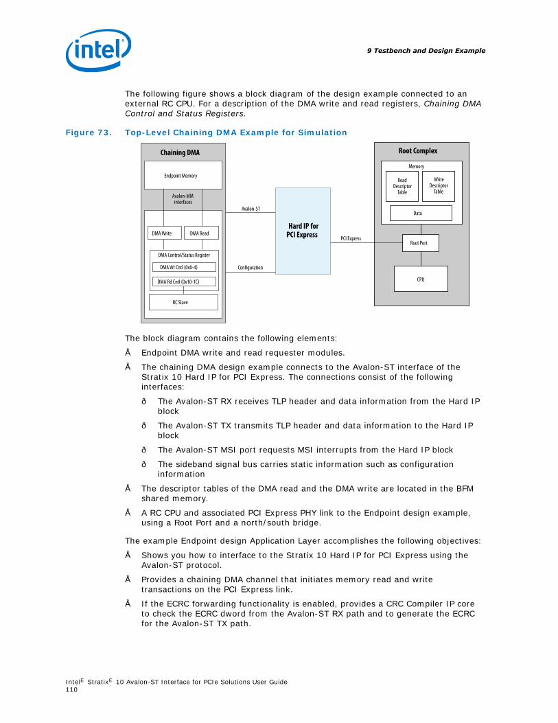
The following figure shows a block diagram of the design example connected to anexternal RC CPU. For a description of the DMA write and read registers, Chaining DMAControl and Status Registers.
Figure 73. Top-Level Chaining DMA Example for Simulation
Root Complex
CPU
Root Port
Memory
WriteDescriptor
Table
Data
Chaining DMA
Endpoint Memory
Avalon-MM interfaces
Hard IP forPCI Express
DMA Control/Status Register
DMA Read
Avalon-ST
Configuration
PCI Express DMA Write
DMA Wr Cntl (0x0-4)
DMA Rd Cntl (0x10-1C)
RC Slave
ReadDescriptor
Table
The block diagram contains the following elements:
• Endpoint DMA write and read requester modules.
• The chaining DMA design example connects to the Avalon-ST interface of theStratix 10 Hard IP for PCI Express. The connections consist of the followinginterfaces:
— The Avalon-ST RX receives TLP header and data information from the Hard IPblock
— The Avalon-ST TX transmits TLP header and data information to the Hard IPblock
— The Avalon-ST MSI port requests MSI interrupts from the Hard IP block
— The sideband signal bus carries static information such as configurationinformation
• The descriptor tables of the DMA read and the DMA write are located in the BFMshared memory.
• A RC CPU and associated PCI Express PHY link to the Endpoint design example,using a Root Port and a north/south bridge.
The example Endpoint design Application Layer accomplishes the following objectives:
• Shows you how to interface to the Stratix 10 Hard IP for PCI Express using theAvalon-ST protocol.
• Provides a chaining DMA channel that initiates memory read and writetransactions on the PCI Express link.
• If the ECRC forwarding functionality is enabled, provides a CRC Compiler IP coreto check the ECRC dword from the Avalon-ST RX path and to generate the ECRCfor the Avalon-ST TX path.
9 Testbench and Design Example
Intel® Stratix® 10 Avalon-ST Interface for PCIe Solutions User Guide110

The following modules are included in the design example and located in thesubdirectory <qsys_systemname>/testbench/<qsys_system_name>_tb/simulation/submodules :
• <qsys_systemname> —This module is the top level of the example Endpointdesign that you use for simulation.
This module provides both PIPE and serial interfaces for the simulationenvironment. This module has a test_in debug ports. Refer to Test Signalswhich allow you to monitor and control internal states of the Hard IP.
For synthesis, the top level module is <qsys_systemname>/synthesis/submodules. This module instantiates the top-level module and propagates onlya small sub-set of the test ports to the external I/Os. These test ports can be usedin your design.
• <variation name>.v or <variation name>.vhd— Because Intel provides manysample parameterizations, you may have to edit one of the provided examples tocreate a simulation that matches your requirements. <variation name>.v or<variation name>.vhd— Because Intel provides many sample parameterizations,you may have to edit one of the provided examples to create a simulation thatmatches your requirements.
The chaining DMA design example hierarchy consists of these components:
• A DMA read and a DMA write module
• An on-chip Endpoint memory (Avalon-MM slave) which uses two Avalon-MMinterfaces for each engine
The RC slave module is used primarily for downstream transactions which target theEndpoint on-chip buffer memory. These target memory transactions bypass the DMAengines. In addition, the RC slave module monitors performance and acknowledgesincoming message TLPs. Each DMA module consists of these components:
• Control register module—The RC programs the control register (four dwords) tostart the DMA.
• Descriptor module—The DMA engine fetches four dword descriptors from BFMshared memory which hosts the chaining DMA descriptor table.
• Requester module—For a given descriptor, the DMA engine performs the memorytransfer between Endpoint memory and the BFM shared memory.
9 Testbench and Design Example
Intel® Stratix® 10 Avalon-ST Interface for PCIe Solutions User Guide111

The following modules are provided in both Verilog HDL:
• altpcierd_example_app_chaining—This top level module contains the logicrelated to the Avalon-ST interfaces as well as the logic related to the sidebandbus. This module is fully register bounded and can be used as an incremental re-compile partition in the Quartus Prime compilation flow.
• altpcierd_cdma_ast_rx, altpcierd_cdma_ast_rx_64,altpcierd_cdma_ast_rx_128—These modules implement the Avalon-ST receiveport for the chaining DMA. The Avalon-ST receive port converts the Avalon-STinterface of the IP core to the descriptor/data interface used by the chaining DMAsubmodules. altpcierd_cdma_ast_rx is used with the descriptor/data IP core(through the ICM). a ltpcierd_cdma_ast_rx_64 is used with the 64-bit Avalon-ST IP core. altpcierd_cdma_ast_rx_128 is used with the 128-bit Avalon-ST IPcore.
• altpcierd_cdma_ast_tx, altpcierd_cdma_ast_tx_64,altpcierd_cdma_ast_tx_128—These modules implement the Avalon-STtransmit port for the chaining DMA. The Avalon-ST transmit port converts thedescriptor/data interface of the chaining DMA submodules to the Avalon-STinterface of the IP core. altpcierd_cdma_ast_tx is used with the descriptor/dataIP core (through the ICM). altpcierd_cdma_ast_tx_64 is used with the 64-bitAvalon-ST IP core. altpcierd_cdma_ast_tx_128 is used with the 128-bitAvalon-ST IP core.
• altpcierd_cdma_ast_msi—This module converts MSI requests from the chainingDMA submodules into Avalon-ST streaming data.
• alpcierd_cdma_app_icm—This module arbitrates PCI Express packets for themodules altpcierd_dma_dt (read or write) and altpcierd_rc_slave.alpcierd_cdma_app_icm instantiates the Endpoint memory used for the DMAread and write transfer.
• alt pcierd_compliance_test.v—This module provides the logic to perform CBBvia a push button.
• altpcierd_rc_slave—This module provides the completer function for alldownstream accesses. It instantiates the altpcierd_rxtx_downstream_intf andaltpcierd_reg_ access modules. Downstream requests include programming ofchaining DMA control registers, reading of DMA status registers, and direct readand write access to the Endpoint target memory, bypassing the DMA.
• altpcierd_rx_tx_downstream_intf—This module processes all downstreamread and write requests and handles transmission of completions. Requestsaddressed to BARs 0, 1, 4, and 5 access the chaining DMA target memory space.Requests addressed to BARs 2 and 3 access the chaining DMA control and statusregister space using the altpcierd_reg_access module.
• altpcierd_reg_access—This module provides access to all of the chaining DMAcontrol and status registers (BAR 2 and 3 address space). It provides addressdecoding for all requests and multiplexing for completion data. All registers are32-bits wide. Control and status registers include the control registers in thealtpcierd_dma_prg_reg module, status registers in thealtpcierd_read_dma_requester and altpcierd_write_dma_requestermodules, as well as other miscellaneous status registers.
• altpcierd_dma_dt—This module arbitrates PCI Express packets issued by thesubmodules altpcierd_dma_prg_reg, altpcierd_read_dma_requester,altpcierd_write_dma_requester and altpcierd_dma_descriptor.
9 Testbench and Design Example
Intel® Stratix® 10 Avalon-ST Interface for PCIe Solutions User Guide112

• altpcierd_dma_prg_reg —This module contains the chaining DMA controlregisters which get programmed by the software application or BFM driver.
• altpcierd_dma_descriptor—This module retrieves the DMA read or writedescriptor from the BFM shared memory, and stores it in a descriptor FIFO. Thismodule issues upstream PCI Express TLPs of type MRd.
• altpcierd_read_dma_requester, altpcierd_read_dma_requester_128—Foreach descriptor located in the altpcierd_descriptor FIFO, this module transfersdata from the BFM shared memory to the Endpoint memory by issuing MRd PCIExpress transaction layer packets. altpcierd_read_dma_requester is used withthe 64-bit Avalon-ST IP core. altpcierd_read_dma_requester_128 is used withthe 128-bit Avalon-ST IP core.
• altpcie rd_write_dma_requester, altpcierd_write_dma_requester_128—For each descriptor located in the altpcierd_descriptor FIFO, this moduletransfers data from the Endpoint memory to the BFM shared memory by issuingMWr PCI Express transaction layer packets. altpcierd_write_dma_requester isused with the 64-bit Avalon-ST IP core. altpcierd_write_dma_requester_128is used with the 128-bit Avalon-ST IP core.ls
• altpcierd_cpld_rx_buffer—This modules monitors the available space of the RXBuffer; It prevents RX Buffer overflow by arbitrating memory read request issuedby the application.
• altpcierd_cplerr_lmi—This module transfers the err_desc_func0 from theapplication to the Hard IP block using the LMI interface. It also retimes thecpl_err bits from the application to the Hard IP block.
• altpcierd_tl_cfg_sample—This module demultiplexes the Configuration Spacesignals from the tl_cfg_ctl bus from the Hard IP block and synchronizes thisinformation, along with the tl_cfg_sts bus to the user clock (pld_clk)domain.
Related Links
Chaining DMA Control and Status Registers on page 114
9.2.1 BAR/Address Map
The design example maps received memory transactions to either the target memoryblock or the control register block based on which BAR the transaction matches. Thereare multiple BARs that map to each of these blocks to maximize interoperability withdifferent variation files. The following table shows the mapping.
Table 65. BAR Map
Memory BAR Mapping
32-bit BAR032-bit BAR164-bit BAR1:0
Maps to 32 KB target memory block. Use the rc_slave module to bypass the chainingDMA.
32-bit BAR232-bit BAR364-bit BAR3:2
Maps to DMA Read and DMA write control and status registers, a minimum of 256bytes.
32-bit BAR432-bit BAR5
Maps to 32 KB target memory block. Use the rc_slave module to bypass the chainingDMA.
continued...
9 Testbench and Design Example
Intel® Stratix® 10 Avalon-ST Interface for PCIe Solutions User Guide113

Memory BAR Mapping
64-bit BAR5:4
Expansion ROM BAR Not implemented by design example; behavior is unpredictable.
I/O Space BAR (any) Not implemented by design example; behavior is unpredictable.
9.2.2 Chaining DMA Control and Status Registers
The software application programs the chaining DMA control register located in theEndpoint application. The following table describes the control registers which consistsof four dwords for the DMA write and four dwords for the DMA read. The DMA controlregisters are read/write.
In this table, Addr specifies the Endpoint byte address offset from BAR2 or BAR3.
Table 66. Chaining DMA Control Register Definitions
Addr Register Name Bits[31:]24 Bit[23:16] Bit[15:0]
0x0 DMA Wr Cntl DW0 Control Field Number of descriptorsin descriptor table
0x4 DMA Wr Cntl DW1 Base Address of the Write Descriptor Table (BDT) in the RC Memory–UpperDWORD
0x8 DMA Wr Cntl DW2 Base Address of the Write Descriptor Table (BDT) in the RC Memory–LowerDWORD
0xC DMA Wr Cntl DW3 Reserved Reserved RCLAST–Idx of lastdescriptor to process
0x10 DMA Rd Cntl DW0 Control Field (described in the next table) Number of descriptorsin descriptor table
0x14 DMA Rd Cntl DW1 Base Address of the Read Descriptor Table (BDT) in the RC Memory–UpperDWORD
0x18 DMA Rd Cntl DW2 Base Address of the Read Descriptor Table (BDT) in the RC Memory–LowerDWORD
0x1C DMA Rd Cntl DW3 Reserved Reserved RCLAST–Idx of the lastdescriptor to process
The following table describes the control fields of the of the DMA read and DMA writecontrol registers.
Table 67. Bit Definitions for the Control Field in the DMA Write Control Register andDMA Read Control Register
Bit Field Description
16 Reserved —
17 MSI_ENA Enables interrupts of all descriptors. When 1, the Endpoint DMA moduleissues an interrupt using MSI to the RC when each descriptor iscompleted. Your software application or BFM driver can use this interruptto monitor the DMA transfer status.
18 EPLAST_ENA Enables the Endpoint DMA module to write the number of each descriptorback to the EPLAST field in the descriptor table.
continued...
9 Testbench and Design Example
Intel® Stratix® 10 Avalon-ST Interface for PCIe Solutions User Guide114

Bit Field Description
[24:20] MSI Number When your RC reads the MSI capabilities of the Endpoint, these registerbits map to the back-end MSI signals app_msi_num [4:0]. If there ismore than one MSI, the default mapping if all the MSIs are available, is:• MSI 0 = Read• MSI 1 = Write
[30:28] MSI Traffic Class When the RC application software reads the MSI capabilities of theEndpoint, this value is assigned by default to MSI traffic class 0. Theseregister bits map to the back-end signal app_msi_tc[2:0].
31 DT RC Last Sync When 0, the DMA engine stops transfers when the last descriptor hasbeen executed. When 1, the DMA engine loops infinitely restarting withthe first descriptor when the last descriptor is completed. To stop theinfinite loop, set this bit to 0.
The following table defines the DMA status registers. These registers are read only. Inthis table, Addr specifies the Endpoint byte address offset from BAR2 or BAR3.
Table 68. Chaining DMA Status Register Definitions
Addr Register Name Bits[31:24] Bits[23:16] Bits[15:0]
0x20 DMA Wr Status Hi For field definitions refer to Fields in the DMA Write Status High Registerbelow.
0x24 DMA Wr Status Lo Target Mem AddressWidth
Write DMA Performance Counter. (Clock cyclesfrom time DMA header programmed until lastdescriptor completes, including time to fetchdescriptors.)
0x28 DMA Rd Status Hi For field definitions refer to Fields in the DMA Read Status High Registerbelow.
0x2C DMA Rd Status Lo Max No. of Tags Read DMA Performance Counter. The number ofclocks from the time the DMA header isprogrammed until the last descriptorcompletes, including the time to fetchdescriptors.
0x30 Error Status Reserved Error Counter. Numberof bad ECRCs detectedby the ApplicationLayer. Valid only whenECRC forwarding isenabled.
The following table describes the fields of the DMA write status register. All of thesefields are read only.
Table 69. Fields in the DMA Write Status High Register
Bit Field Description
[31:28] CDMA version Identifies the version of the chaining DMA example design.
[27:24] Reserved —
[23:21] Max payload size The following encodings are defined:• 001 128 bytes• 001 256 bytes• 010 512 bytes• 011 1024 bytes• 100 2048 bytes
continued...
9 Testbench and Design Example
Intel® Stratix® 10 Avalon-ST Interface for PCIe Solutions User Guide115
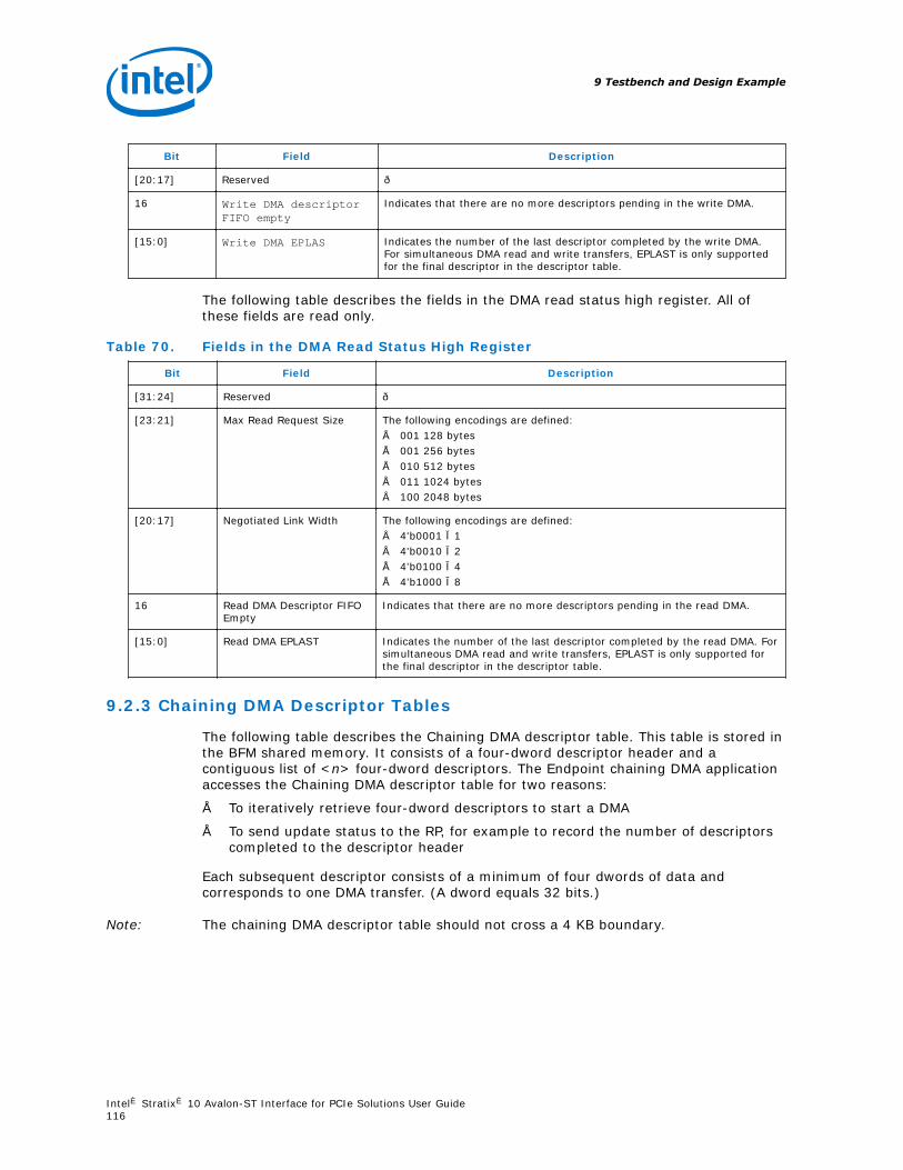
Bit Field Description
[20:17] Reserved —
16 Write DMA descriptorFIFO empty
Indicates that there are no more descriptors pending in the write DMA.
[15:0] Write DMA EPLAS Indicates the number of the last descriptor completed by the write DMA.For simultaneous DMA read and write transfers, EPLAST is only supportedfor the final descriptor in the descriptor table.
The following table describes the fields in the DMA read status high register. All ofthese fields are read only.
Table 70. Fields in the DMA Read Status High Register
Bit Field Description
[31:24] Reserved —
[23:21] Max Read Request Size The following encodings are defined:• 001 128 bytes• 001 256 bytes• 010 512 bytes• 011 1024 bytes• 100 2048 bytes
[20:17] Negotiated Link Width The following encodings are defined:• 4'b0001 ×1• 4'b0010 ×2• 4'b0100 ×4• 4'b1000 ×8
16 Read DMA Descriptor FIFOEmpty
Indicates that there are no more descriptors pending in the read DMA.
[15:0] Read DMA EPLAST Indicates the number of the last descriptor completed by the read DMA. Forsimultaneous DMA read and write transfers, EPLAST is only supported forthe final descriptor in the descriptor table.
9.2.3 Chaining DMA Descriptor Tables
The following table describes the Chaining DMA descriptor table. This table is stored inthe BFM shared memory. It consists of a four-dword descriptor header and acontiguous list of <n> four-dword descriptors. The Endpoint chaining DMA applicationaccesses the Chaining DMA descriptor table for two reasons:
• To iteratively retrieve four-dword descriptors to start a DMA
• To send update status to the RP, for example to record the number of descriptorscompleted to the descriptor header
Each subsequent descriptor consists of a minimum of four dwords of data andcorresponds to one DMA transfer. (A dword equals 32 bits.)
Note: The chaining DMA descriptor table should not cross a 4 KB boundary.
9 Testbench and Design Example
Intel® Stratix® 10 Avalon-ST Interface for PCIe Solutions User Guide116
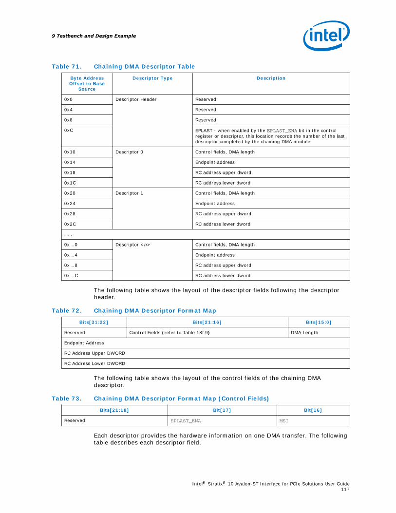
Table 71. Chaining DMA Descriptor Table
Byte AddressOffset to Base
Source
Descriptor Type Description
0x0 Descriptor Header Reserved
0x4 Reserved
0x8 Reserved
0xC EPLAST - when enabled by the EPLAST_ENA bit in the controlregister or descriptor, this location records the number of the lastdescriptor completed by the chaining DMA module.
0x10 Descriptor 0 Control fields, DMA length
0x14 Endpoint address
0x18 RC address upper dword
0x1C RC address lower dword
0x20 Descriptor 1 Control fields, DMA length
0x24 Endpoint address
0x28 RC address upper dword
0x2C RC address lower dword
. . .
0x ..0 Descriptor <n> Control fields, DMA length
0x ..4 Endpoint address
0x ..8 RC address upper dword
0x ..C RC address lower dword
The following table shows the layout of the descriptor fields following the descriptorheader.
Table 72. Chaining DMA Descriptor Format Map
Bits[31:22] Bits[21:16] Bits[15:0]
Reserved Control Fields (refer to Table 18–9) DMA Length
Endpoint Address
RC Address Upper DWORD
RC Address Lower DWORD
The following table shows the layout of the control fields of the chaining DMAdescriptor.
Table 73. Chaining DMA Descriptor Format Map (Control Fields)
Bits[21:18] Bit[17] Bit[16]
Reserved EPLAST_ENA MSI
Each descriptor provides the hardware information on one DMA transfer. The followingtable describes each descriptor field.
9 Testbench and Design Example
Intel® Stratix® 10 Avalon-ST Interface for PCIe Solutions User Guide117
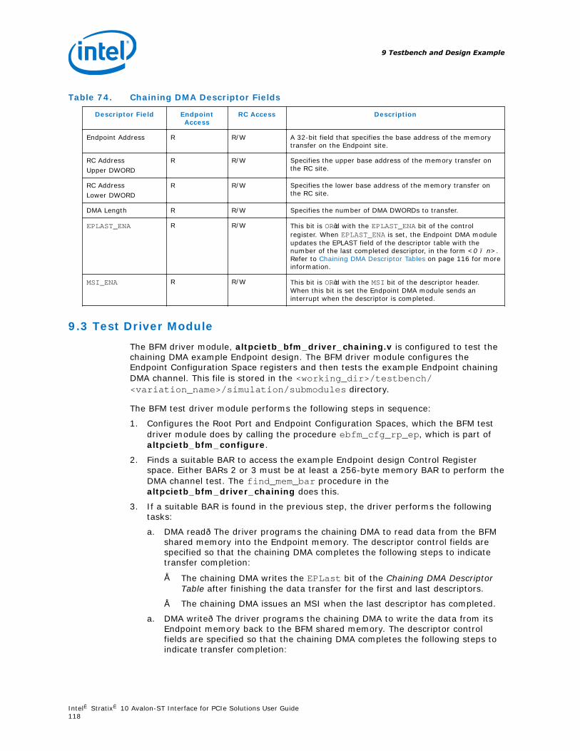
Table 74. Chaining DMA Descriptor Fields
Descriptor Field EndpointAccess
RC Access Description
Endpoint Address R R/W A 32-bit field that specifies the base address of the memorytransfer on the Endpoint site.
RC AddressUpper DWORD
R R/W Specifies the upper base address of the memory transfer onthe RC site.
RC AddressLower DWORD
R R/W Specifies the lower base address of the memory transfer onthe RC site.
DMA Length R R/W Specifies the number of DMA DWORDs to transfer.
EPLAST_ENA R R/W This bit is OR’d with the EPLAST_ENA bit of the controlregister. When EPLAST_ENA is set, the Endpoint DMA moduleupdates the EPLAST field of the descriptor table with thenumber of the last completed descriptor, in the form <0 – n>.Refer to Chaining DMA Descriptor Tables on page 116 for moreinformation.
MSI_ENA R R/W This bit is OR’d with the MSI bit of the descriptor header.When this bit is set the Endpoint DMA module sends aninterrupt when the descriptor is completed.
9.3 Test Driver Module
The BFM driver module, altpcietb_bfm_driver_chaining.v is configured to test thechaining DMA example Endpoint design. The BFM driver module configures theEndpoint Configuration Space registers and then tests the example Endpoint chainingDMA channel. This file is stored in the <working_dir>/testbench/<variation_name>/simulation/submodules directory.
The BFM test driver module performs the following steps in sequence:
1. Configures the Root Port and Endpoint Configuration Spaces, which the BFM testdriver module does by calling the procedure ebfm_cfg_rp_ep, which is part ofaltpcietb_bfm_configure.
2. Finds a suitable BAR to access the example Endpoint design Control Registerspace. Either BARs 2 or 3 must be at least a 256-byte memory BAR to perform theDMA channel test. The find_mem_bar procedure in thealtpcietb_bfm_driver_chaining does this.
3. If a suitable BAR is found in the previous step, the driver performs the followingtasks:
a. DMA read—The driver programs the chaining DMA to read data from the BFMshared memory into the Endpoint memory. The descriptor control fields arespecified so that the chaining DMA completes the following steps to indicatetransfer completion:
• The chaining DMA writes the EPLast bit of the Chaining DMA DescriptorTable after finishing the data transfer for the first and last descriptors.
• The chaining DMA issues an MSI when the last descriptor has completed.
a. DMA write—The driver programs the chaining DMA to write the data from itsEndpoint memory back to the BFM shared memory. The descriptor controlfields are specified so that the chaining DMA completes the following steps toindicate transfer completion:
9 Testbench and Design Example
Intel® Stratix® 10 Avalon-ST Interface for PCIe Solutions User Guide118

• The chaining DMA writes the EPLast bit of the Chaining DMA DescriptorTable after completing the data transfer for the first and last descriptors.
• The chaining DMA issues an MSI when the last descriptor has completed.
• The data written back to BFM is checked against the data that was readfrom the BFM.
• The driver programs the chaining DMA to perform a test thatdemonstrates downstream access of the chaining DMA Endpoint memory.
Note: Edit this file if you want to add your own custom PCIe transactions. Insert your owncustom function after the find_mem_bar function. You can use the functions in theBFM Procedures and Functions section.
Related Links
• Chaining DMA Descriptor Tables on page 116
• BFM Procedures and Functions on page 130
9.4 DMA Write Cycles
The procedure dma_wr_test used for DMA writes uses the following steps:
1. Configures the BFM shared memory. Configuration is accomplished with threedescriptor tables described below.
Table 75. Write Descriptor 0
Offset in BFMin SharedMemory
Value Description
DW0 0x810 82 Transfer length in dwords and control bits as described in BitDefinitions for the Control Field in the DMA Write Control Register andDMA Read Control Register.
DW1 0x814 3 Endpoint address
DW2 0x818 0 BFM shared memory data buffer 0 upper address value
DW3 0x81c 0x1800 BFM shared memory data buffer 1 lower address value
Data Buffer0
0x1800 Increment by 1from0x1515_0001
Data content in the BFM shared memory from address: 0x01800–0x1840
Table 76. Write Descriptor 1
Offset in BFMSharedMemory
Value Description
DW0 0x820 1,024 Transfer length in dwords and control bits as described in BitDefinitions for the Control Field in the DMA Write Control Register andDMA Read Control Register .
DW1 0x824 0 Endpoint address
continued...
9 Testbench and Design Example
Intel® Stratix® 10 Avalon-ST Interface for PCIe Solutions User Guide119
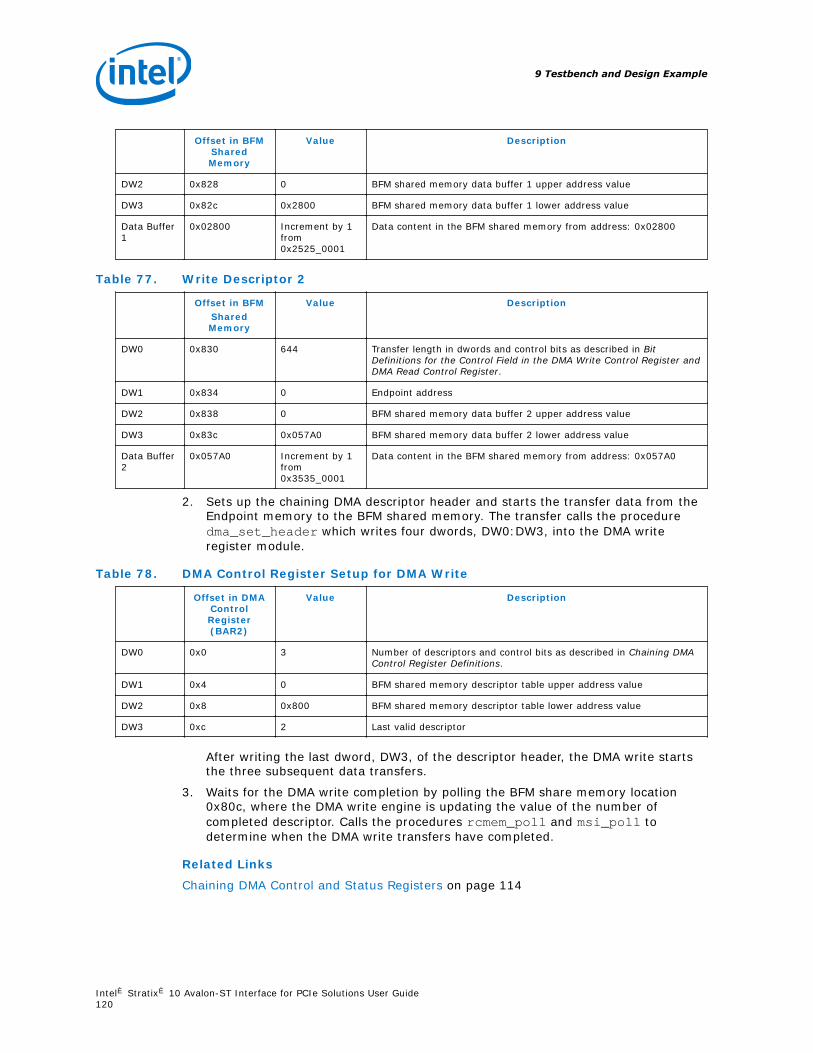
Offset in BFMSharedMemory
Value Description
DW2 0x828 0 BFM shared memory data buffer 1 upper address value
DW3 0x82c 0x2800 BFM shared memory data buffer 1 lower address value
Data Buffer1
0x02800 Increment by 1from0x2525_0001
Data content in the BFM shared memory from address: 0x02800
Table 77. Write Descriptor 2
Offset in BFMSharedMemory
Value Description
DW0 0x830 644 Transfer length in dwords and control bits as described in BitDefinitions for the Control Field in the DMA Write Control Register andDMA Read Control Register.
DW1 0x834 0 Endpoint address
DW2 0x838 0 BFM shared memory data buffer 2 upper address value
DW3 0x83c 0x057A0 BFM shared memory data buffer 2 lower address value
Data Buffer2
0x057A0 Increment by 1from0x3535_0001
Data content in the BFM shared memory from address: 0x057A0
2. Sets up the chaining DMA descriptor header and starts the transfer data from theEndpoint memory to the BFM shared memory. The transfer calls the proceduredma_set_header which writes four dwords, DW0:DW3, into the DMA writeregister module.
Table 78. DMA Control Register Setup for DMA Write
Offset in DMAControlRegister(BAR2)
Value Description
DW0 0x0 3 Number of descriptors and control bits as described in Chaining DMAControl Register Definitions.
DW1 0x4 0 BFM shared memory descriptor table upper address value
DW2 0x8 0x800 BFM shared memory descriptor table lower address value
DW3 0xc 2 Last valid descriptor
After writing the last dword, DW3, of the descriptor header, the DMA write startsthe three subsequent data transfers.
3. Waits for the DMA write completion by polling the BFM share memory location0x80c, where the DMA write engine is updating the value of the number ofcompleted descriptor. Calls the procedures rcmem_poll and msi_poll todetermine when the DMA write transfers have completed.
Related Links
Chaining DMA Control and Status Registers on page 114
9 Testbench and Design Example
Intel® Stratix® 10 Avalon-ST Interface for PCIe Solutions User Guide120
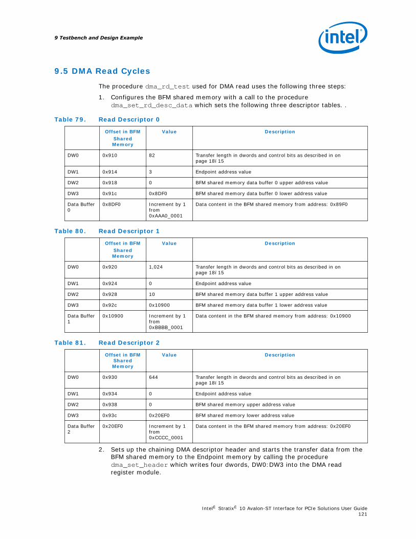
9.5 DMA Read Cycles
The procedure dma_rd_test used for DMA read uses the following three steps:
1. Configures the BFM shared memory with a call to the proceduredma_set_rd_desc_data which sets the following three descriptor tables. .
Table 79. Read Descriptor 0
Offset in BFMSharedMemory
Value Description
DW0 0x910 82 Transfer length in dwords and control bits as described in onpage 18–15
DW1 0x914 3 Endpoint address value
DW2 0x918 0 BFM shared memory data buffer 0 upper address value
DW3 0x91c 0x8DF0 BFM shared memory data buffer 0 lower address value
Data Buffer0
0x8DF0 Increment by 1from0xAAA0_0001
Data content in the BFM shared memory from address: 0x89F0
Table 80. Read Descriptor 1
Offset in BFMSharedMemory
Value Description
DW0 0x920 1,024 Transfer length in dwords and control bits as described in onpage 18–15
DW1 0x924 0 Endpoint address value
DW2 0x928 10 BFM shared memory data buffer 1 upper address value
DW3 0x92c 0x10900 BFM shared memory data buffer 1 lower address value
Data Buffer1
0x10900 Increment by 1from0xBBBB_0001
Data content in the BFM shared memory from address: 0x10900
Table 81. Read Descriptor 2
Offset in BFMSharedMemory
Value Description
DW0 0x930 644 Transfer length in dwords and control bits as described in onpage 18–15
DW1 0x934 0 Endpoint address value
DW2 0x938 0 BFM shared memory upper address value
DW3 0x93c 0x20EF0 BFM shared memory lower address value
Data Buffer2
0x20EF0 Increment by 1from0xCCCC_0001
Data content in the BFM shared memory from address: 0x20EF0
2. Sets up the chaining DMA descriptor header and starts the transfer data from theBFM shared memory to the Endpoint memory by calling the proceduredma_set_header which writes four dwords, DW0:DW3 into the DMA readregister module.
9 Testbench and Design Example
Intel® Stratix® 10 Avalon-ST Interface for PCIe Solutions User Guide121

Table 82. DMA Control Register Setup for DMA Read
Offset in DMA ControlRegisters (BAR2)
Value Description
DW0 0x0 3 Number of descriptors and control bits as described in Chaining DMAControl Register Definitions.
DW1 0x14 0 BFM shared memory upper address value
DW2 0x18 0x900 BFM shared memory lower address value
DW3 0x1c 2 Last descriptor written
After writing the last dword of the Descriptor header (DW3), the DMA read startsthe three subsequent data transfers.
3. Waits for the DMA read completion by polling the BFM shared memory location0x90c, where the DMA read engine is updating the value of the number ofcompleted descriptors. Calls the procedures rcmem_poll and msi_poll todetermine when the DMA read transfers have completed.
9.6 Root Port BFM
The basic Root Port BFM provides Verilog HDL task-based interface for requestingtransactions that are issued to the PCI Express link. The Root Port BFM also handlesrequests received from the PCI Express link. The following figure provides an overviewof the Root Port BFM.
Figure 74. Root Port BFM
BFM Shared Memory(altpcietb_bfm_shmem
_common)
BFM Log Interface(altpcietb_bfm_log
_common)
Root Port RTL Model (altpcietb_bfm_rp_top_x8_pipen1b)
IP Functional SimulationModel of the Root
Port Interface (altpcietb_bfm_driver_rp)
Avalon-ST Interface(altpcietb_bfm_vc_intf)
Root Port BFM
BFM Read/Write Shared Request Procedures
BFM Configuration Procedures
BFM Request Interface(altpcietb_bfm_req_intf_common)
9 Testbench and Design Example
Intel® Stratix® 10 Avalon-ST Interface for PCIe Solutions User Guide122

The functionality of each of the modules included is explained below.
• BFM shared memory (altpcietb_bfm_shmem_common Verilog HDL include file)—The Root Port BFM is based on the BFM memory that is used for the followingpurposes:
• Storing data received with all completions from the PCI Express link.
• Storing data received with all write transactions received from the PCI Expresslink.
• Sourcing data for all completions in response to read transactions received fromthe PCI Express link.
• Sourcing data for most write transactions issued to the PCI Express link. The onlyexception is certain BFM write procedures that have a four-byte field of write datapassed in the call.
• Storing a data structure that contains the sizes of and the values programmed inthe BARs of the Endpoint.
A set of procedures is provided to read, write, fill, and check the shared memory fromthe BFM driver. For details on these procedures, see BFM Shared Memory AccessProcedures.
• BFM Read/Write Request Functions(altpcietb_bfm_driver_rp.v)—Thesefunctions provide the basic BFM calls for PCI Express read and write requests. Fordetails on these procedures, refer to BFM Read and Write Procedures.
• BFM Configuration Functions(altpcietb_bfm_driver_rp.v )—These functionsprovide the BFM calls to request configuration of the PCI Express link and theEndpoint Configuration Space registers. For details on these procedures andfunctions, refer to BFM Configuration Procedures.
• BFM Log Interface(altpcietb_bfm_driver_rp.v)—The BFM log functionsprovides routines for writing commonly formatted messages to the simulatorstandard output and optionally to a log file. It also provides controls that stopsimulation on errors. For details on these procedures, refer to BFM Log andMessage Procedures.
• BFM Request Interface(altpcietb_bfm_driver_rp.v)—This interface providesthe low-level interface between the altpcietb_bfm_rdwr andaltpcietb_bfm_configure procedures or functions and the Root Port RTLModel. This interface stores a write-protected data structure containing the sizesand the values programmed in the BAR registers of the Endpoint, as well as, othercritical data used for internal BFM management. You do not need to access thesefiles directly to adapt the testbench to test your Endpoint application.
• Avalon-ST Interfaces (altpcietb_bfm_vc_intf.v)—These interface moduleshandle the Root Port interface model. They take requests from the BFM requestinterface and generate the required PCI Express transactions. They handlecompletions received from the PCI Express link and notify the BFM requestinterface when requests are complete. Additionally, they handle any requestsreceived from the PCI Express link, and store or fetch data from the sharedmemory before generating the required completions.
Related Links
BFM Shared Memory Access Procedures on page 136
9 Testbench and Design Example
Intel® Stratix® 10 Avalon-ST Interface for PCIe Solutions User Guide123

9.6.1 BFM Memory Map
The BFM shared memory is configured to be two MBs. The BFM shared memory ismapped into the first two MBs of I/O space and also the first two MBs of memoryspace. When the Endpoint application generates an I/O or memory transaction in thisrange, the BFM reads or writes the shared memory.
9.6.2 Configuration Space Bus and Device Numbering
The Root Port interface is assigned to be device number 0 on internal bus number 0.The Endpoint can be assigned to be any device number on any bus number (greaterthan 0) through the call to procedure ebfm_cfg_rp_ep. The specified bus number isassigned to be the secondary bus in the Root Port Configuration Space.
9.6.3 Configuration of Root Port and Endpoint
Before you issue transactions to the Endpoint, you must configure the Root Port andEndpoint Configuration Space registers. To configure these registers, call theprocedure ebfm_cfg_rp_ep, which is included in altpcietb_bfm_driver_rp.v.
The ebfm_cfg_rp_ep executes the following steps to initialize the ConfigurationSpace:
1. Sets the Root Port Configuration Space to enable the Root Port to sendtransactions on the PCI Express link.
2. Sets the Root Port and Endpoint PCI Express Capability Device Control registers asfollows:
a. Disables Error Reporting in both the Root Port and Endpoint. BFM does nothave error handling capability.
b. Enables Relaxed Ordering in both Root Port and Endpoint.
c. Enables Extended Tags for the Endpoint, if the Endpoint has that capability.
d. Disables Phantom Functions, Aux Power PM, and No Snoop in both theRoot Port and Endpoint.
e. Sets the Max Payload Size to what the Endpoint supports because the RootPort supports the maximum payload size.
f. Sets the Root Port Max Read Request Size to 4 KB because the exampleEndpoint design supports breaking the read into as many completions asnecessary.
g. Sets the Endpoint Max Read Request Size equal to the Max Payload Sizebecause the Root Port does not support breaking the read request intomultiple completions.
3. Assigns values to all the Endpoint BAR registers. The BAR addresses are assignedby the algorithm outlined below.
9 Testbench and Design Example
Intel® Stratix® 10 Avalon-ST Interface for PCIe Solutions User Guide124

a. I/O BARs are assigned smallest to largest starting just above the endingaddress of BFM shared memory in I/O space and continuing as neededthroughout a full 32-bit I/O space.
b. The 32-bit non-prefetchable memory BARs are assigned smallest to largest,starting just above the ending address of BFM shared memory in memoryspace and continuing as needed throughout a full 32-bit memory space.
c. Assignment of the 32-bit prefetchable and 64-bit prefetchable memory BARSare based on the value of the addr_map_4GB_limit input to theebfm_cfg_rp_ep. The default value of the addr_map_4GB_limit is 0.
If the addr_map_4GB_limit input to the ebfm_cfg_rp_ep is set to 0, thenthe 32-bit prefetchable memory BARs are assigned largest to smallest,starting at the top of 32-bit memory space and continuing as needed down tothe ending address of the last 32-bit non-prefetchable BAR.
However, if the addr_map_4GB_limit input is set to 1, the address map islimited to 4 GB, the 32-bit and 64-bit prefetchable memory BARs are assignedlargest to smallest, starting at the top of the 32-bit memory space andcontinuing as needed down to the ending address of the last 32-bit non-prefetchable BAR.
d. If the addr_map_4GB_limit input to the ebfm_cfg_rp_ep is set to 0, thenthe 64-bit prefetchable memory BARs are assigned smallest to largest startingat the 4 GB address assigning memory ascending above the 4 GB limitthroughout the full 64-bit memory space.
If the addr_map_4 GB_limit input to the ebfm_cfg_rp_ep is set to 1, thenthe 32-bit and the 64-bit prefetchable memory BARs are assigned largest tosmallest starting at the 4 GB address and assigning memory by descendingbelow the 4 GB address to addresses memory as needed down to the endingaddress of the last 32-bit non-prefetchable BAR.
The above algorithm cannot always assign values to all BARs when there are afew very large (1 GB or greater) 32-bit BARs. Although assigning addresses toall BARs may be possible, a more complex algorithm would be required toeffectively assign these addresses. However, such a configuration is unlikely tobe useful in real systems. If the procedure is unable to assign the BARs, itdisplays an error message and stops the simulation.
4. Based on the above BAR assignments, the Root Port Configuration Space addresswindows are assigned to encompass the valid BAR address ranges.
5. The Endpoint PCI control register is set to enable master transactions, memoryaddress decoding, and I/O address decoding.
The ebfm_cfg_rp_ep procedure also sets up a bar_table data structure in BFMshared memory that lists the sizes and assigned addresses of all Endpoint BARs. Thisarea of BFM shared memory is write-protected, which means any user write accessesto this area cause a fatal simulation error. This data structure is then used bysubsequent BFM procedure calls to generate the full PCI Express addresses for readand write requests to particular offsets from a BAR. This procedure allows thetestbench code that accesses the Endpoint Application Layer to be written to useoffsets from a BAR and not have to keep track of the specific addresses assigned tothe BAR. The following table shows how those offsets are used.
9 Testbench and Design Example
Intel® Stratix® 10 Avalon-ST Interface for PCIe Solutions User Guide125

Table 83. BAR Table Structure
Offset (Bytes) Description
+0 PCI Express address in BAR0
+4 PCI Express address in BAR1
+8 PCI Express address in BAR2
+12 PCI Express address in BAR3
+16 PCI Express address in BAR4
+20 PCI Express address in BAR5
+24 PCI Express address in Expansion ROM BAR
+28 Reserved
+32 BAR0 read back value after being written with all 1’s (used to compute size)
+36 BAR1 read back value after being written with all 1’s
+40 BAR2 read back value after being written with all 1’s
+44 BAR3 read back value after being written with all 1’s
+48 BAR4 read back value after being written with all 1’s
+52 BAR5 read back value after being written with all 1’s
+56 Expansion ROM BAR read back value after being written with all 1’s
+60 Reserved
The configuration routine does not configure any advanced PCI Express capabilitiessuch as the AER capability.
Besides the ebfm_cfg_rp_ep procedure in altpcietb_bfm_driver_rp.v, routines toread and write Endpoint Configuration Space registers directly are available in theVerilog HDL include file. After the ebfm_cfg_rp_ep procedure is run the PCI ExpressI/O and Memory Spaces have the layout as described in the following three figures.The memory space layout is dependent on the value of the add r_map_4GB_limitinput parameter. If addr_map_4GB_limit is 1 the resulting memory space map isshown in the following figure.
9 Testbench and Design Example
Intel® Stratix® 10 Avalon-ST Interface for PCIe Solutions User Guide126
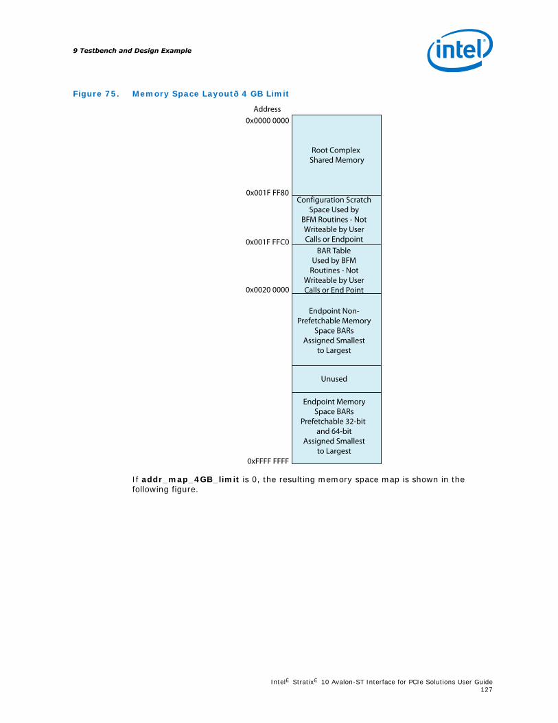
Figure 75. Memory Space Layout—4 GB Limit
Root Complex Shared Memory
Unused
Configuration ScratchSpace Used by
BFM Routines - NotWriteable by UserCalls or Endpoint
BAR TableUsed by BFM
Routines - NotWriteable by UserCalls or End Point
Endpoint Non-Prefetchable Memory
Space BARsAssigned Smallest
to Largest
Endpoint MemorySpace BARs
Prefetchable 32-bit and 64-bit
Assigned Smallestto Largest
0xFFFF FFFF
0x0020 0000
0x0000 0000Address
0x001F FFC0
0x001F FF80
If addr_map_4GB_limit is 0, the resulting memory space map is shown in thefollowing figure.
9 Testbench and Design Example
Intel® Stratix® 10 Avalon-ST Interface for PCIe Solutions User Guide127

Figure 76. Memory Space Layout—No Limit
Root Complex Shared Memory
Unused
Unused
Configuration ScratchSpace Used byRoutines - Not
Writeable by UserCalls or Endpoint
BAR TableUsed by BFM
Routines - NotWriteable by UserCalls or Endpoint
Endpoint Non-Prefetchable Memory
Space BARsAssigned Smallest
to Largest
Endpoint MemorySpace BARs
Prefetchable 64-bit Assigned Smallest
to Largest
Endpoint MemorySpace BARs
Prefetchable 32-bit Assigned Smallest
to Largest
BAR-Size Dependent
BAR-Size Dependent
BAR-Size Dependent
0x0000 0001 0000 0000
0xFFFF FFFF FFFF FFFF
0x0020 0000
0x0000 0000Address
0x001F FF00
0x001F FF80
The following figure shows the I/O address space.
9 Testbench and Design Example
Intel® Stratix® 10 Avalon-ST Interface for PCIe Solutions User Guide128

Figure 77. I/O Address Space
Root Complex Shared Memory
Unused
Configuration ScratchSpace Used by BFM
Routines - NotWriteable by UserCalls or Endpoint
BAR TableUsed by BFM
Routines - NotWriteable by UserCalls or Endpoint
Endpoint I/O Space BARs
Assigned Smallestto Largest
BAR-Size Dependent
0xFFFF FFFF
0x0020 0000
0x0000 0000Address
0x001F FFC0
0x001F FF80
9 Testbench and Design Example
Intel® Stratix® 10 Avalon-ST Interface for PCIe Solutions User Guide129

9.6.4 Issuing Read and Write Transactions to the Application Layer
Read and write transactions are issued to the Endpoint Application Layer by calling oneof the ebfm_bar procedures in altpcietb_bfm_driver_rp.v. The procedures andfunctions listed below are available in the Verilog HDL include filealtpcietb_bfm_driver_rp.v. The complete list of available procedures and functionsis as follows:
• ebfm_barwr—writes data from BFM shared memory to an offset from a specificEndpoint BAR. This procedure returns as soon as the request has been passed tothe VC interface module for transmission.
• ebfm_barwr_imm—writes a maximum of four bytes of immediate data (passed ina procedure call) to an offset from a specific Endpoint BAR. This procedure returnsas soon as the request has been passed to the VC interface module fortransmission.
• ebfm_barrd_wait—reads data from an offset of a specific Endpoint BAR andstores it in BFM shared memory. This procedure blocks waiting for the completiondata to be returned before returning control to the caller.
• ebfm_barrd_nowt—reads data from an offset of a specific Endpoint BAR andstores it in the BFM shared memory. This procedure returns as soon as the requesthas been passed to the VC interface module for transmission, allowing subsequentreads to be issued in the interim.
These routines take as parameters a BAR number to access the memory space andthe BFM shared memory address of the bar_table data structure that was set up bythe ebfm_cfg_rp_ep procedure. (Refer to Configuration of Root Port and Endpoint.)Using these parameters simplifies the BFM test driver routines that access an offsetfrom a specific BAR and eliminates calculating the addresses assigned to the specifiedBAR.
The Root Port BFM does not support accesses to Endpoint I/O space BARs.
Related Links
Configuration of Root Port and Endpoint on page 124
9.7 BFM Procedures and Functions
The BFM includes procedures, functions, and tasks to drive Endpoint applicationtesting. It also includes procedures to run the chaining DMA design example.
The BFM read and write procedures read and write data among BFM shared memory,Endpoint BARs, and specified configuration registers. The procedures and functions areavailable in the Verilog HDL. They are in the include file altpcietb_bfm_driver.v.These procedures and functions support issuing memory and configurationtransactions on the PCI Express link.
9.7.1 ebfm_barwr Procedure
The ebfm_barwr procedure writes a block of data from BFM shared memory to anoffset from the specified Endpoint BAR. The length can be longer than the configuredMAXIMUM_PAYLOAD_SIZE; the procedure breaks the request up into multipletransactions as needed. This routine returns as soon as the last transaction has beenaccepted by the VC interface module.
9 Testbench and Design Example
Intel® Stratix® 10 Avalon-ST Interface for PCIe Solutions User Guide130

Location altpcietb_bfm_rdwr.v
Syntax ebfm_barwr(bar_table, bar_num, pcie_offset, lcladdr, byte_len, tclass)
Arguments bar_table Address of the Endpoint bar_table structure in BFM shared memory.The bar_table structure stores the address assigned to each BAR sothat the driver code does not need to be aware of the actual assignedaddresses only the application specific offsets from the BAR.
bar_num Number of the BAR used with pcie_offset to determine PCI Expressaddress.
pcie_offset Address offset from the BAR base.
lcladdr BFM shared memory address of the data to be written.
byte_len Length, in bytes, of the data written. Can be 1 to the minimum of thebytes remaining in the BAR space or BFM shared memory.
tclass Traffic class used for the PCI Express transaction.
9.7.2 ebfm_barwr_imm Procedure
The ebfm_barwr_imm procedure writes up to four bytes of data to an offset from thespecified Endpoint BAR.
Location altpcietb_bfm_driver_rp.v
Syntax ebfm_barwr_imm(bar_table, bar_num, pcie_offset, imm_data, byte_len, tclass)
Arguments bar_table Address of the Endpoint bar_table structure in BFM shared memory.The bar_table structure stores the address assigned to each BAR sothat the driver code does not need to be aware of the actual assignedaddresses only the application specific offsets from the BAR.
bar_num Number of the BAR used with pcie_offset to determine PCI Expressaddress.
pcie_offset Address offset from the BAR base.
imm_data Data to be written. In Verilog HDL, this argument is reg [31:0].Inboth languages, the bits written depend on the length as follows:Length Bits Written• 4: 31 downto 0• 3: 23 downto 0• 2: 15 downto 0• 1: 7 downto 0
byte_len Length of the data to be written in bytes. Maximum length is 4 bytes.
tclass Traffic class to be used for the PCI Express transaction.
9.7.3 ebfm_barrd_wait Procedure
The ebfm_barrd_wait procedure reads a block of data from the offset of thespecified Endpoint BAR and stores it in BFM shared memory. The length can be longerthan the configured maximum read request size; the procedure breaks the request upinto multiple transactions as needed. This procedure waits until all of the completiondata is returned and places it in shared memory.
Location altpcietb_bfm_driver_rp.v
Syntax ebfm_barrd_wait(bar_table, bar_num, pcie_offset, lcladdr, byte_len, tclass)
continued...
9 Testbench and Design Example
Intel® Stratix® 10 Avalon-ST Interface for PCIe Solutions User Guide131

Arguments bar_table Address of the Endpoint bar_table structure in BFM shared memory.The bar_table structure stores the address assigned to each BAR so thatthe driver code does not need to be aware of the actual assignedaddresses only the application specific offsets from the BAR.
bar_num Number of the BAR used with pcie_offset to determine PCI Expressaddress.
pcie_offset Address offset from the BAR base.
lcladdr BFM shared memory address where the read data is stored.
byte_len Length, in bytes, of the data to be read. Can be 1 to the minimum ofthe bytes remaining in the BAR space or BFM shared memory.
tclass Traffic class used for the PCI Express transaction.
9.7.4 ebfm_barrd_nowt Procedure
The ebfm_barrd_nowt procedure reads a block of data from the offset of thespecified Endpoint BAR and stores the data in BFM shared memory. The length can belonger than the configured maximum read request size; the procedure breaks therequest up into multiple transactions as needed. This routine returns as soon as thelast read transaction has been accepted by the VC interface module, allowingsubsequent reads to be issued immediately.
Location altpcietb_b fm_driver_rp.v
Syntax ebfm_barrd_nowt(bar_table, bar_num, pcie_offset, lcladdr, byte_len, tclass)
Arguments bar_table Address of the Endpoint bar_table structure in BFM shared memory.
bar_num Number of the BAR used with pcie_offset to determine PCI Expressaddress.
pcie_offset Address offset from the BAR base.
lcladdr BFM shared memory address where the read data is stored.
byte_len Length, in bytes, of the data to be read. Can be 1 to the minimum ofthe bytes remaining in the BAR space or BFM shared memory.
tclass Traffic Class to be used for the PCI Express transaction.
9.7.5 ebfm_cfgwr_imm_wait Procedure
The ebfm_cfgwr_imm_wait procedure writes up to four bytes of data to thespecified configuration register. This procedure waits until the write completion hasbeen returned.
Location altpcietb_bfm_driver_rp.v
Syntax ebfm_cfgwr_imm_wait(bus_num, dev_num, fnc_num, imm_regb_ad, regb_ln, imm_data,compl_status
Arguments bus_num PCI Express bus number of the target device.
dev_num PCI Express device number of the target device.
fnc_num Function number in the target device to be accessed.
regb_ad Byte-specific address of the register to be written.
continued...
9 Testbench and Design Example
Intel® Stratix® 10 Avalon-ST Interface for PCIe Solutions User Guide132

Location altpcietb_bfm_driver_rp.v
regb_ln Length, in bytes, of the data written. Maximum length is four bytes. Theregb_ln and the regb_ad arguments cannot cross a DWORDboundary.
imm_data Data to be written.This argument is reg [31:0].The bits written depend on the length:• 4: 31 downto 0• 3: 23 downto 0• 2: 15 downto 0• 1: 7 downto 0
compl_status This argument is reg [2:0].This argument is the completion status as specified in the PCI Expressspecification. The following encodings are defined:• 3’b000: SC— Successful completion• 3’b001: UR— Unsupported Request• 3’b010: CRS — Configuration Request Retry Status• 3’b100: CA — Completer Abort
9.7.6 ebfm_cfgwr_imm_nowt Procedure
The ebfm_cfgwr_imm_nowt procedure writes up to four bytes of data to thespecified configuration register. This procedure returns as soon as the VC interfacemodule accepts the transaction, allowing other writes to be issued in the interim. Usethis procedure only when successful completion status is expected.
Location altpcietb_bfm_driver_rp.v
Syntax ebfm_cfgwr_imm_nowt(bus_num, dev_num, fnc_num, imm_regb_adr, regb_len,imm_data)
Arguments bus_num PCI Express bus number of the target device.
dev_num PCI Express device number of the target device.
fnc_num Function number in the target device to be accessed.
regb_ad Byte-specific address of the register to be written.
regb_ln Length, in bytes, of the data written. Maximum length is four bytes, Theregb_ln the regb_ad arguments cannot cross a DWORD boundary.
imm_data Data to be writtenThis argument is reg [31:0].In both languages, the bits written depend on the length. The followingencodes are defined.• 4: [31:0]• 3: [23:0]• 2: [15:0]• 1: [7:0]
9.7.7 ebfm_cfgrd_wait Procedure
The ebfm_cfgrd_wait procedure reads up to four bytes of data from the specifiedconfiguration register and stores the data in BFM shared memory. This procedurewaits until the read completion has been returned.
9 Testbench and Design Example
Intel® Stratix® 10 Avalon-ST Interface for PCIe Solutions User Guide133

Location altpcietb_bfm_driver_rp.v
Syntax ebfm_cfgrd_wait(bus_num, dev_num, fnc_num, regb_ad, regb_ln, lcladdr,compl_status)
Arguments bus_num PCI Express bus number of the target device.
dev_num PCI Express device number of the target device.
fnc_num Function number in the target device to be accessed.
regb_ad Byte-specific address of the register to be written.
regb_ln Length, in bytes, of the data read. Maximum length is four bytes. Theregb_ln and the regb_ad arguments cannot cross a DWORDboundary.
lcladdr BFM shared memory address of where the read data should be placed.
compl_status Completion status for the configuration transaction.This argument is reg [2:0].In both languages, this is the completion status as specified in the PCIExpress specification. The following encodings are defined.• 3’b000: SC— Successful completion• 3’b001: UR— Unsupported Request• 3’b010: CRS — Configuration Request Retry Status• 3’b100: CA — Completer Abort
9.7.8 ebfm_cfgrd_nowt Procedure
The ebfm_cfgrd_nowt procedure reads up to four bytes of data from the specifiedconfiguration register and stores the data in the BFM shared memory. This procedurereturns as soon as the VC interface module has accepted the transaction, allowingother reads to be issued in the interim. Use this procedure only when successfulcompletion status is expected and a subsequent read or write with a wait can be usedto guarantee the completion of this operation.
Location altpcietb_bfm_driver_rp.v
Syntax ebfm_cfgrd_nowt(bus_num, dev_num, fnc_num, regb_ad, regb_ln, lcladdr)
Arguments bus_num PCI Express bus number of the target device.
dev_num PCI Express device number of the target device.
fnc_num Function number in the target device to be accessed.
regb_ad Byte-specific address of the register to be written.
regb_ln Length, in bytes, of the data written. Maximum length is four bytes. Theregb_ln and regb_ad arguments cannot cross a DWORD boundary.
lcladdr BFM shared memory address where the read data should be placed.
9.7.9 BFM Configuration Procedures
The BFM configuration procedures are available in altpcietb_bfm_driver_rp.v.These procedures support configuration of the Root Port and Endpoint ConfigurationSpace registers.
All Verilog HDL arguments are type integer and are input-only unless specifiedotherwise.
9 Testbench and Design Example
Intel® Stratix® 10 Avalon-ST Interface for PCIe Solutions User Guide134

9.7.9.1 ebfm_cfg_rp_ep Procedure
The ebfm_cfg_rp_ep procedure configures the Root Port and Endpoint ConfigurationSpace registers for operation.
Location altpcietb_bfm_driver_rp.v
Syntax ebfm_cfg_rp_ep(bar_table, ep_bus_num, ep_dev_num, rp_max_rd_req_size,display_ep_config, addr_map_4GB_limit)
Arguments bar_table Address of the Endpoint bar_table structure in BFM shared memory.This routine populates the bar_table structure. The bar_tablestructure stores the size of each BAR and the address values assigned toeach BAR. The address of the bar_table structure is passed to allsubsequent read and write procedure calls that access an offset from aparticular BAR.
ep_bus_num PCI Express bus number of the target device. This number can be anyvalue greater than 0. The Root Port uses this as its secondary busnumber.
ep_dev_num PCI Express device number of the target device. This number can beany value. The Endpoint is automatically assigned this value when itreceives its first configuration transaction.
rp_max_rd_req_size Maximum read request size in bytes for reads issued by the Root Port.This parameter must be set to the maximum value supported by theEndpoint Application Layer. If the Application Layer only supports readsof the MAXIMUM_PAYLOAD_SIZE, then this can be set to 0 and the readrequest size will be set to the maximum payload size. Valid values forthis argument are 0, 128, 256, 512, 1,024, 2,048 and 4,096.
display_ep_config When set to 1 many of the Endpoint Configuration Space registers aredisplayed after they have been initialized, causing some additional readsof registers that are not normally accessed during the configurationprocess such as the Device ID and Vendor ID.
addr_map_4GB_limit When set to 1 the address map of the simulation system will be limitedto 4 GB. Any 64-bit BARs will be assigned below the 4 GB limit.
9.7.9.2 ebfm_cfg_decode_bar Procedure
The ebfm_cfg_decode_bar procedure analyzes the information in the BAR table forthe specified BAR and returns details about the BAR attributes.
Location altpcietb_bfm_driver_rp.v
Syntax ebfm_cfg_decode_bar(bar_table, bar_num, log2_size, is_mem, is_pref, is_64b)
Arguments bar_table Address of the Endpoint bar_table structure in BFM shared memory.
bar_num BAR number to analyze.
log2_size This argument is set by the procedure to the log base 2 of the size ofthe BAR. If the BAR is not enabled, this argument will be set to 0.
is_mem The procedure sets this argument to indicate if the BAR is a memoryspace BAR (1) or I/O Space BAR (0).
is_pref The procedure sets this argument to indicate if the BAR is a prefetchableBAR (1) or non-prefetchable BAR (0).
is_64b The procedure sets this argument to indicate if the BAR is a 64-bit BAR(1) or 32-bit BAR (0). This is set to 1 only for the lower numbered BARof the pair.
9 Testbench and Design Example
Intel® Stratix® 10 Avalon-ST Interface for PCIe Solutions User Guide135

9.7.10 BFM Shared Memory Access Procedures
The BFM shared memory access procedures and functions are in the Verilog HDLinclude file altpcietb_bfm_driver.v. These procedures and functions supportaccessing the BFM shared memory.
9.7.10.1 Shared Memory Constants
The following constants are defined in altpcietb_bfm_driver.v. They select a datapattern in the shmem_fill and shmem_chk_ok routines. These shared memoryconstants are all Verilog HDL type integer.
Table 84. Constants: Verilog HDL Type INTEGER
Constant Description
SHMEM_FILL_ZEROS Specifies a data pattern of all zeros
SHMEM_FILL_BYTE_INC Specifies a data pattern of incrementing 8-bit bytes (0x00, 0x01, 0x02,etc.)
SHMEM_FILL_WORD_INC Specifies a data pattern of incrementing 16-bit words (0x0000, 0x0001,0x0002, etc.)
SHMEM_FILL_DWORD_INC Specifies a data pattern of incrementing 32-bit dwords (0x00000000,0x00000001, 0x00000002, etc.)
SHMEM_FILL_QWORD_INC Specifies a data pattern of incrementing 64-bit qwords(0x0000000000000000, 0x0000000000000001, 0x0000000000000002,etc.)
SHMEM_FILL_ONE Specifies a data pattern of all ones
9.7.10.2 shmem_write
The shmem_write procedure writes data to the BFM shared memory.
Location altpcietb_bfm_driver_rp.v
Syntax shmem_write(addr, data, leng)
Arguments addr BFM shared memory starting address for writing data
data Data to write to BFM shared memory.This parameter is implemented as a 64-bit vector. leng is 1–8 bytes.Bits 7 downto 0 are written to the location specified by addr; bits 15downto 8 are written to the addr+1 location, etc.
length Length, in bytes, of data written
9.7.10.3 shmem_read Function
The shmem_read function reads data to the BFM shared memory.
Location altpcietb_bfm_driver_rp.v
Syntax data:= shmem_read(addr, leng)
Arguments addr BFM shared memory starting address for reading data
leng Length, in bytes, of data read
Return data Data read from BFM shared memory.
continued...
9 Testbench and Design Example
Intel® Stratix® 10 Avalon-ST Interface for PCIe Solutions User Guide136

Location altpcietb_bfm_driver_rp.v
This parameter is implemented as a 64-bit vector. leng is 1- 8 bytes. Ifleng is less than 8 bytes, only the corresponding least significant bits ofthe returned data are valid.Bits 7 downto 0 are read from the location specified by addr; bits 15downto 8 are read from the addr+1 location, etc.
9.7.10.4 shmem_display Verilog HDL Function
The shmem_display Verilog HDL function displays a block of data from the BFMshared memory.
Location altpcietb_bfm_driver_rp.v
Syntax Verilog HDL: dummy_return:=shmem_display(addr, leng, word_size, flag_addr,msg_type);
Arguments addr BFM shared memory starting address for displaying data.
leng Length, in bytes, of data to display.
word_size Size of the words to display. Groups individual bytes into words. Validvalues are 1, 2, 4, and 8.
flag_addr Adds a <== flag to the end of the display line containing this address.Useful for marking specific data. Set to a value greater than 2**21 (sizeof BFM shared memory) to suppress the flag.
msg_type Specifies the message type to be displayed at the beginning of eachline. See “BFM Log and Message Procedures” on page 18–37 for moreinformation about message types. Set to one of the constants defined inTable 18–36 on page 18–41.
9.7.10.5 shmem_fill Procedure
The shmem_fill procedure fills a block of BFM shared memory with a specified datapattern.
Location altpcietb_bfm_driver_rp.v
Syntax shmem_fill(addr, mode, leng, init)
Arguments addr BFM shared memory starting address for filling data.
mode Data pattern used for filling the data. Should be one of the constantsdefined in section Shared Memory Constants.
leng Length, in bytes, of data to fill. If the length is not a multiple of theincrementing data pattern width, then the last data pattern is truncatedto fit.
init Initial data value used for incrementing data pattern modes. Thisargument is reg [63:0].The necessary least significant bits are used for the data patterns thatare smaller than 64 bits.
Related Links
Shared Memory Constants on page 136
9.7.10.6 shmem_chk_ok Function
The shmem_chk_ok function checks a block of BFM shared memory against aspecified data pattern.
9 Testbench and Design Example
Intel® Stratix® 10 Avalon-ST Interface for PCIe Solutions User Guide137

Location altpcietb_bfm_shmem.v
Syntax result:= shmem_chk_ok(addr, mode, leng, init, display_error)
Arguments addr BFM shared memory starting address for checking data.
mode Data pattern used for checking the data. Should be one of the constantsdefined in section “Shared Memory Constants” on page 18–35.
leng Length, in bytes, of data to check.
init This argument is reg [63:0].The necessary least significant bits areused for the data patterns that are smaller than 64-bits.
display_error When set to 1, this argument displays the miscomparing data on thesimulator standard output.
Return Result Result is 1-bit.• 1’b1 — Data patterns compared successfully• 1’b0 — Data patterns did not compare successfully
9.7.11 BFM Log and Message Procedures
The following procedures and functions are available in the Verilog HDL include filealtpcietb_bfm_driver_rp.v.
These procedures provide support for displaying messages in a common format,suppressing informational messages, and stopping simulation on specific messagetypes.
The following constants define the type of message and their values determinewhether a message is displayed or simulation is stopped after a specific message.Each displayed message has a specific prefix, based on the message type in thefollowing table.
You can suppress the display of certain message types. The default values determiningwhether a message type is displayed are defined in the following table. To change thedefault message display, modify the display default value with a procedure call toebfm_log_set_suppressed_msg_mask.
Certain message types also stop simulation after the message is displayed. Thefollowing table shows the default value determining whether a message type stopssimulation. You can specify whether simulation stops for particular messages with theprocedure ebfm_log_set_stop_on_msg_mask.
All of these log message constants type integer.
Table 85. Log Messages
Constant(Message
Type)
Description Mask BitNo
Displayby Default
SimulationStops byDefault
MessagePrefix
EBFM_MSG_DEBUG
Specifies debug messages. 0 No No DEBUG:
EBFM_MSG_INFO
Specifies informational messages,such as configuration registervalues, starting and ending of tests.
1 Yes No INFO:
continued...
9 Testbench and Design Example
Intel® Stratix® 10 Avalon-ST Interface for PCIe Solutions User Guide138

Constant(Message
Type)
Description Mask BitNo
Displayby Default
SimulationStops byDefault
MessagePrefix
EBFM_MSG_WARNING
Specifies warning messages, suchas tests being skipped due to thespecific configuration.
2 Yes No WARNING:
EBFM_MSG_ERROR_INFO
Specifies additional information foran error. Use this message todisplay preliminary informationbefore an error message that stopssimulation.
3 Yes No ERROR:
EBFM_MSG_ERROR_CONTINUE
Specifies a recoverable error thatallows simulation to continue. Usethis error for data miscompares.
4 Yes No ERROR:
EBFM_MSG_ERROR_FATAL
Specifies an error that stopssimulation because the error leavesthe testbench in a state wherefurther simulation is not possible.
N/A YesCannotsuppress
YesCannot suppress
FATAL:
EBFM_MSG_ERROR_FATAL_TB_ERR
Used for BFM test driver or RootPort BFM fatal errors. Specifies anerror that stops simulation becausethe error leaves the testbench in astate where further simulation isnot possible. Use this errormessage for errors that occur dueto a problem in the BFM test drivermodule or the Root Port BFM, thatare not caused by the EndpointApplication Layer being tested.
N/A YCannotsuppress
YCannot suppress
FATAL:
9.7.11.1 ebfm_display Verilog HDL Function
The ebfm_display procedure or function displays a message of the specified type tothe simulation standard output and also the log file if ebfm_log_open is called.
A message can be suppressed, simulation can be stopped or both based on the defaultsettings of the message type and the value of the bit mask when each of theprocedures listed below is called. You can call one or both of these procedures basedon what messages you want displayed and whether or not you want simulation to stopfor specific messages.
• When ebfm_log_set_suppressed_msg_mask is called, the display of themessage might be suppressed based on the value of the bit mask.
• When ebfm_log_set_stop_on_msg_mask is called, the simulation can bestopped after the message is displayed, based on the value of the bit mask.
Location altpcietb_bfm_driver_rp.v
Syntax Verilog HDL: dummy_return:=ebfm_display(msg_type, message);
Argument msg_type Message type for the message. Should be one of the constants definedin Table 18–36 on page 18–41.
message The message string is limited to a maximum of 100 characters. Also,because Verilog HDL does not allow variable length strings, this routinestrips off leading characters of 8’h00 before displaying the message.
Return always 0 Applies only to the Verilog HDL routine.
9 Testbench and Design Example
Intel® Stratix® 10 Avalon-ST Interface for PCIe Solutions User Guide139

9.7.11.2 ebfm_log_stop_sim Verilog HDL Function
The ebfm_log_stop_sim procedure stops the simulation.
Location altpcietb_bfm_driver_rp.v
Syntax Verilog HDL: return:=ebfm_log_stop_sim(success);
Argument success When set to a 1, this process stops the simulation with a messageindicating successful completion. The message is prefixed withSUCCESS:.Otherwise, this process stops the simulation with a message indicatingunsuccessful completion. The message is prefixed with FAILURE:.
Return Always 0 This value applies only to the Verilog HDL function.
9.7.11.3 ebfm_log_set_suppressed_msg_mask #Verilog HDL Function
The ebfm_log_set_suppressed_msg_mask procedure controls which messagetypes are suppressed.
Location altpcietb_bfm_driver_rp.v
Syntax bfm_log_set_suppressed_msg_mask (msg_mask)
Argument msg_mask This argument is reg [EBFM_MSG_ERROR_CONTINUE:EBFM_MSG_DEBUG].
A 1 in a specific bit position of the msg_mask causes messages of thetype corresponding to the bit position to be suppressed.
9.7.11.4 ebfm_log_set_stop_on_msg_mask Verilog HDL Function
The ebfm_log_set_stop_on_msg_mask procedure controls which message typesstop simulation. This procedure alters the default behavior of the simulation whenerrors occur as described in the BFM Log and Message Procedures.
Location altpcietb_bfm_driver_rp.v
Syntax ebfm_log_set_stop_on_msg_mask (msg_mask)
Argument msg_mask This argument is reg[EBFM_MSG_ERROR_CONTINUE:EBFM_MSG_DEBUG].A 1 in a specific bit position of the msg_mask causes messages of thetype corresponding to the bit position to stop the simulation after themessage is displayed.
Related Links
BFM Log and Message Procedures on page 138
9.7.11.5 ebfm_log_open Verilog HDL Function
The ebfm_log_open procedure opens a log file of the specified name. All displayedmessages are called by ebfm_display and are written to this log file as simulatorstandard output.
Location altpcietb_bfm_driver_rp.v
Syntax ebfm_log_open (fn)
Argument fn This argument is type string and provides the file name of log file tobe opened.
9 Testbench and Design Example
Intel® Stratix® 10 Avalon-ST Interface for PCIe Solutions User Guide140
9.7.11.6 ebfm_log_close Verilog HDL Function
The ebfm_log_close procedure closes the log file opened by a previous call toebfm_log_open.
Location altpcietb_bfm_driver_rp.v
Syntax ebfm_log_close
Argument NONE
9.7.12 Verilog HDL Formatting Functions
The Verilog HDL Formatting procedures and functions are available in thealtpcietb_bfm_driver_rp.v. The formatting functions are only used by Verilog HDL.All these functions take one argument of a specified length and return a vector of aspecified length.
9.7.12.1 himage1
This function creates a one-digit hexadecimal string representation of the inputargument that can be concatenated into a larger message string and passed toebfm_display.
Location altpcietb_bfm_driver_rp.v
Syntax string:= himage(vec)
Argument vec Input data type reg with a range of 3:0.
Return range string Returns a 1-digit hexadecimal representation of the input argument.Return data is type reg with a range of 8:1
9.7.12.2 himage2
This function creates a two-digit hexadecimal string representation of the inputargument that can be concatenated into a larger message string and passed toebfm_display.
Location altpcietb_bfm_driver_rp.v
Syntax string:= himage(vec)
Argument range vec Input data type reg with a range of 7:0.
Return range string Returns a 2-digit hexadecimal presentation of the input argument,padded with leading 0s, if they are needed. Return data is type reg witha range of 16:1
9.7.12.3 himage4
This function creates a four-digit hexadecimal string representation of the inputargument can be concatenated into a larger message string and passed toebfm_display.
9 Testbench and Design Example
Intel® Stratix® 10 Avalon-ST Interface for PCIe Solutions User Guide141

Location altpcietb_bfm_driver_rp.v
Syntax string:= himage(vec)
Argument range vec Input data type reg with a range of 15:0.
Return range Returns a four-digit hexadecimal representation of the input argument, padded with leading 0s, if theyare needed. Return data is type reg with a range of 32:1.
9.7.12.4 himage8
This function creates an 8-digit hexadecimal string representation of the inputargument that can be concatenated into a larger message string and passed toebfm_display.
Location altpcietb_bfm_driver_rp.v
Syntax string:= himage(vec)
Argument range vec Input data type reg with a range of 31:0.
Return range string Returns an 8-digit hexadecimal representation of the input argument,padded with leading 0s, if they are needed. Return data is type reg witha range of 64:1.
9.7.12.5 himage16
This function creates a 16-digit hexadecimal string representation of the inputargument that can be concatenated into a larger message string and passed toebfm_display.
Location altpcietb_bfm_driver_rp.v
Syntax string:= himage(vec)
Argument range vec Input data type reg with a range of 63:0.
Return range string Returns a 16-digit hexadecimal representation of the input argument,padded with leading 0s, if they are needed. Return data is type reg witha range of 128:1.
9.7.12.6 dimage1
This function creates a one-digit decimal string representation of the input argumentthat can be concatenated into a larger message string and passed to ebfm_display.
Location altpcietb_bfm_driver_rp.v
Syntax string:= dimage(vec)
Argument range vec Input data type reg with a range of 31:0.
Return range string Returns a 1-digit decimal representation of the input argument that ispadded with leading 0s if necessary. Return data is type reg with arange of 8:1.Returns the letter U if the value cannot be represented.
9.7.12.7 dimage2
This function creates a two-digit decimal string representation of the input argumentthat can be concatenated into a larger message string and passed to ebfm_display.
9 Testbench and Design Example
Intel® Stratix® 10 Avalon-ST Interface for PCIe Solutions User Guide142
Location altpcietb_bfm_driver_rp.v
Syntax string:= dimage(vec)
Argument range vec Input data type reg with a range of 31:0.
Return range string Returns a 2-digit decimal representation of the input argument that ispadded with leading 0s if necessary. Return data is type reg with arange of 16:1.Returns the letter U if the value cannot be represented.
9.7.12.8 dimage3
This function creates a three-digit decimal string representation of the input argumentthat can be concatenated into a larger message string and passed to ebfm_display.
Location altpcietb_bfm_driver_rp.v
Syntax string:= dimage(vec)
Argument range vec Input data type reg with a range of 31:0.
Return range string Returns a 3-digit decimal representation of the input argument that ispadded with leading 0s if necessary. Return data is type reg with arange of 24:1.Returns the letter U if the value cannot be represented.
9.7.12.9 dimage4
This function creates a four-digit decimal string representation of the input argumentthat can be concatenated into a larger message string and passed to ebfm_display.
Location altpcietb_bfm_driver_rp.v
Syntax string:= dimage(vec)
Argument range vec Input data type reg with a range of 31:0.
Return range string Returns a 4-digit decimal representation of the input argument that ispadded with leading 0s if necessary. Return data is type reg with arange of 32:1.Returns the letter U if the value cannot be represented.
9.7.12.10 dimage5
This function creates a five-digit decimal string representation of the input argumentthat can be concatenated into a larger message string and passed to ebfm_display.
Location altpcietb_bfm_driver_rp.v
Syntax string:= dimage(vec)
Argument range vec Input data type reg with a range of 31:0.
Return range string Returns a 5-digit decimal representation of the input argument that ispadded with leading 0s if necessary. Return data is type reg with arange of 40:1.Returns the letter U if the value cannot be represented.
9 Testbench and Design Example
Intel® Stratix® 10 Avalon-ST Interface for PCIe Solutions User Guide143
9.7.12.11 dimage6
This function creates a six-digit decimal string representation of the input argumentthat can be concatenated into a larger message string and passed to ebfm_display.
Location altpcietb_bfm_log.v
Syntax string:= dimage(vec)
Argument range vec Input data type reg with a range of 31:0.
Return range string Returns a 6-digit decimal representation of the input argument that ispadded with leading 0s if necessary. Return data is type reg with arange of 48:1.Returns the letter U if the value cannot be represented.
9.7.12.12 dimage7
This function creates a seven-digit decimal string representation of the input argumentthat can be concatenated into a larger message string and passed to ebfm_display.
Location altpcietb_bfm_log.v
Syntax string:= dimage(vec)
Argument range vec Input data type reg with a range of 31:0.
Return range string Returns a 7-digit decimal representation of the input argument that ispadded with leading 0s if necessary. Return data is type reg with arange of 56:1.Returns the letter <U> if the value cannot be represented.
9.7.13 Procedures and Functions Specific to the Chaining DMA DesignExample
The procedures specific to the chaining DMA design example are in the Verilog HDLmodule file altpcietb_bfm_driver_rp.v.
9.7.13.1 chained_dma_test Procedure
The chained_dma_test procedure is the top-level procedure that runs the chainingDMA read and the chaining DMA write
Location altpcietb_bfm_driver_rp.v
Syntax chained_dma_test (bar_table, bar_num, direction, use_msi, use_eplast)
Arguments bar_table Address of the Endpoint bar_table structure in BFM shared memory.
bar_num BAR number to analyze.
direction When 0 the direction is read.When 1 the direction is write.
Use_msi When set, the Root Port uses native PCI Express MSI to detect the DMAcompletion.
Use_eplast When set, the Root Port uses BFM shared memory polling to detect theDMA completion.
9 Testbench and Design Example
Intel® Stratix® 10 Avalon-ST Interface for PCIe Solutions User Guide144

9.7.13.2 dma_rd_test Procedure
Use the dma_rd_test procedure for DMA reads from the Endpoint memory to theBFM shared memory.
Location altpcietb_bfm_driver_rp.v
Syntax dma_rd_test (bar_table, bar_num, use_msi, use_eplast)
Arguments bar_table Address of the Endpoint bar_table structure in BFM shared memory.
bar_num BAR number to analyze.
Use_msi When set, the Root Port uses native PCI express MSI to detect the DMAcompletion.
Use_eplast When set, the Root Port uses BFM shared memory polling to detect theDMA completion.
9.7.13.3 dma_wr_test Procedure
Use the dma_wr_test procedure for DMA writes from the BFM shared memory to theEndpoint memory.
Location altpcietb_bfm_driver_rp.v
Syntax dma_wr_test (bar_table, bar_num, use_msi, use_eplast)
Arguments bar_table Address of the Endpoint bar_table structure in BFM shared memory.
bar_num BAR number to analyze.
Use_msi When set, the Root Port uses native PCI Express MSI to detect the DMAcompletion.
Use_eplast When set, the Root Port uses BFM shared memory polling to detect theDMA completion.
9.7.13.4 dma_set_rd_desc_data Procedure
Use the dma_set_rd_desc_data procedure to configure the BFM shared memory forthe DMA read.
Location altpcietb_bfm_driver_rp.v
Syntax dma_set_rd_desc_data (bar_table, bar_num)
Arguments bar_table Address of the Endpoint bar_table structure in BFM shared memory.
bar_num BAR number to analyze.
9.7.13.5 dma_set_wr_desc_data Procedure
Use the dma_set_wr_desc_data procedure to configure the BFM shared memory forthe DMA write.
Location altpcietb_bfm_driver_rp.v
Syntax dma_set_wr_desc_data_header (bar_table, bar_num)
Arguments bar_table Address of the Endpoint bar_table structure in BFM shared memory.
bar_num BAR number to analyze.
9 Testbench and Design Example
Intel® Stratix® 10 Avalon-ST Interface for PCIe Solutions User Guide145

9.7.13.6 dma_set_header Procedure
Use the dma_set_header procedure to configure the DMA descriptor table for DMAread or DMA write.
Location altpcietb_bfm_driver_rp.v
Syntax dma_set_header (bar_table, bar_num, Descriptor_size, direction, Use_msi,Use_eplast, Bdt_msb, Bdt_lab, Msi_number, Msi_traffic_class,Multi_message_enable)
Arguments bar_table Address of the Endpoint bar_table structure in BFM shared memory.
bar_num BAR number to analyze.
Descriptor_size Number of descriptor.
direction When 0 the direction is read.When 1 the direction is write.
Use_msi When set, the Root Port uses native PCI Express MSI to detect the DMAcompletion.
Use_eplast When set, the Root Port uses BFM shared memory polling to detect theDMA completion.
Bdt_msb BFM shared memory upper address value.
Bdt_lsb BFM shared memory lower address value.
Msi_number When use_msi is set, specifies the number of the MSI which is set bythe dma_set_msi procedure.
Msi_traffic_class When use_msi is set, specifies the MSI traffic class which is set by thedma_set_msi procedure.
Multi_message_enable When use_msi is set, specifies the MSI traffic class which is set by thedma_set_msi procedure.
9.7.13.7 rc_mempoll Procedure
Use the rc_mempoll procedure to poll a given dword in a given BFM shared memorylocation.
Location altpcietb_bfm_driver_rp.v
Syntax rc_mempoll (rc_addr, rc_data, rc_mask)
Arguments rc_addr Address of the BFM shared memory that is being polled.
rc_data Expected data value of the that is being polled.
rc_mask Mask that is logically ANDed with the shared memory data before it iscompared with rc_data.
9.7.13.8 msi_poll Procedure
The msi_poll procedure tracks MSI completion from the Endpoint.
Location altpcietb_bfm_driver_rp.v
Syntax msi_poll(max_number_of_msi,msi_address,msi_expected_dmawr,msi_expected_dmard,dma_write,dma_read)
Arguments max_number_of_msi Specifies the number of MSI interrupts to wait for.
continued...
9 Testbench and Design Example
Intel® Stratix® 10 Avalon-ST Interface for PCIe Solutions User Guide146

Location altpcietb_bfm_driver_rp.v
msi_address The shared memory location to which the MSI messages will be written.
msi_expected_dmawr When dma_write is set, this specifies the expected MSI data value forthe write DMA interrupts which is set by the dma_set_msi procedure.
msi_expected_dmard When the dma_read is set, this specifies the expected MSI data valuefor the read DMA interrupts which is set by the dma_set_msiprocedure.
Dma_write When set, poll for MSI from the DMA write module.
Dma_read When set, poll for MSI from the DMA read module.
9.7.13.9 dma_set_msi Procedure
The dma_set_msi procedure sets PCI Express native MSI for the DMA read or theDMA write.
Location altpcietb_bfm_driver_rp.v
Syntax dma_set_msi(bar_table, bar_num, bus_num, dev_num, fun_num, direction,msi_address, msi_data, msi_number, msi_traffic_class, multi_message_enable,msi_expected)
Arguments bar_table Address of the Endpoint bar_table structure in BFM shared memory.
bar_num BAR number to analyze.
Bus_num Set configuration bus number.
dev_num Set configuration device number.
Fun_num Set configuration function number.
Direction When 0 the direction is read.When 1 the direction is write.
msi_address Specifies the location in shared memory where the MSI message datawill be stored.
msi_data The 16-bit message data that will be stored when an MSI message issent. The lower bits of the message data will be modified with themessage number as per the PCI specifications.
Msi_number Returns the MSI number to be used for these interrupts.
Msi_traffic_class Returns the MSI traffic class value.
Multi_message_enable Returns the MSI multi message enable status.
msi_expected Returns the expected MSI data value, which is msi_data modified bythe msi_number chosen.
9.7.13.10 find_mem_bar Procedure
The find_mem_bar procedure locates a BAR which satisfies a given memory spacerequirement.
Location altpcietb_bfm_driver_rp.v
Syntax Find_mem_bar(bar_table,allowed_bars,min_log2_size, sel_bar)
Arguments bar_table Address of the Endpoint bar_table structure in BFM shared memory
continued...
9 Testbench and Design Example
Intel® Stratix® 10 Avalon-ST Interface for PCIe Solutions User Guide147

Location altpcietb_bfm_driver_rp.v
allowed_bars One hot 6 bits BAR selection
min_log2_size Number of bit required for the specified address space
sel_bar BAR number to use
9.7.13.11 dma_set_rclast Procedure
The dma_set_rclast procedure starts the DMA operation by writing to the EndpointDMA register the value of the last descriptor to process (RCLast).
Location altpcietb_bfm_driver_rp.v
Syntax Dma_set_rclast(bar_table, setup_bar, dt_direction, dt_rclast)
Arguments bar_table Address of the Endpoint bar_table structure in BFM shared memory
setup_bar BAR number to use
dt_direction When 0 read, When 1 write
dt_rclast Last descriptor number
9.7.13.12 ebfm_display_verb Procedure
The ebfm_display_verb procedure calls the procedure ebfm_display when theglobal variable DISPLAY_ALL is set to 1.
Location altpcietb_bfm_driver_chaining.v
Syntax ebfm_display_verb(msg_type, message)
Arguments msg_type Message type for the message. Should be one of the constants definedin BFM Log and Message Procedures.
message The message string is limited to a maximum of 100 characters. Also,because Verilog HDL does not allow variable length strings, this routinestrips off leading characters of 8'h00 before displaying the message.
Related Links
BFM Log and Message Procedures on page 138
9.8 Setting Up Simulation
Changing the simulation parameters reduces simulation time and provides greatervisibility.
9.8.1 Changing Between Serial and PIPE Simulation
By default, the Intel testbench runs a serial simulation. You can change between serialand PIPE simulation by editing the top-level testbench file. For Endpoint designs, thetop-level testbench file is
The serial_sim_hwtcl and enable_pipe32_sim_hwtcl parameters control serialmode or PIPE simulation mode. To change to PIPE mode, changeenable_pipe32_sim_hwtcl to 1'b1 and serial_sim_hwtcl to 1'b0.
9 Testbench and Design Example
Intel® Stratix® 10 Avalon-ST Interface for PCIe Solutions User Guide148

Table 86. Controlling Serial and PIPE Simulations
Data Rates Parameter Settings
serial_sim_hwtcl enable_pipe32_sim_hwtcl
Serial simulation 1 0
PIPE simulation 0 1
9.8.2 Using the PIPE Interface for Gen1 and Gen2 Variants
Running the simulation in PIPE mode reduces simulation time and provides greatervisibility.
Complete the following steps to simulate using the PIPE interface:
1. Change to your simulation directory, <work_dir>/<variant>/testbench/<variant>_tb/simulation
2. Open <variant>_tb.v.
3. Search for the string, serial_sim_hwtcl. Set the value of this parameter to 0 ifit is 1.
4. Save <variant>_tb.v.
9.8.3 Viewing the Important PIPE Interface Signals
You can view the most important PIPE interface signals, txdata, txdatak, rxdata,and rxdatak at the following level of the design hierarchy:altpcie_<device>_hip_pipen1b|twentynm_hssi_<gen>_<lanes>_pcie_hip.
9.8.4 Disabling the Scrambler for Gen1 and Gen2 Simulations
The encoding scheme implemented by the scrambler applies a binary polynomial tothe data stream to ensure enough data transitions between 0 and 1 to prevent clockdrift. The data is decoded at the other end of the link by running the inversepolynomial.
Complete the following steps to disable the scrambler:
1. Open <work_dir>/<variant>/testbench/<variant>_tb/simulation/submodules/altpcie_tbed_<dev>_hwtcl.v.
2. Search for the string, test_in.
3. To disable the scrambler, set test_in[2] = 1.
4. Save altpcie_tbed_sv_hwtcl.v.
9.8.5 Disabling 8B/10B Encoding and Decoding for Gen1 and Gen2Simulations
You can disable 8B/10B encoding and decoding to facilitate debugging.
For Gen1 and Gen2 variants, you can disable 8B/10B encoding and decoding bysetting test_in[2] = 1 in altpcietb_bfm_top_rp.v.
9 Testbench and Design Example
Intel® Stratix® 10 Avalon-ST Interface for PCIe Solutions User Guide149

A Troubleshooting and Observing the Link
A.1 Simulation Fails To Progress Beyond Polling.Active State
If your PIPE simulation cycles between the Detect.Quiet, Detect.Active, andPolling.Active LTSSM states, the PIPE interface width may be incorrect. The width ofthe DUT top-level PIPE interface is 32 bits for Stratix 10 devices.
A.2 Hardware Bring-Up Issues
Typically, PCI Express hardware bring-up involves the following steps:
1. System reset
2. Link training
3. BIOS enumeration
The following sections describe how to debug the hardware bring-up flow. Intelrecommends a systematic approach to diagnosing bring-up issues as illustrated in thefollowing figure.
Figure 78. Debugging Link Training Issues
No
System Reset Does Link Train
Correctly?
Check PIPEInterface
Use PCIe Protocol Analyzer
Soft Reset System to Force Enumeration
Check Configuration Space
Check LTSSMStatus
YesYes
No
SuccessfulOS/BIOS
Enumeration?
A.3 Link Training
The Physical Layer automatically performs link training and initialization withoutsoftware intervention. This is a well-defined process to configure and initialize thedevice's Physical Layer and link so that PCIe packets can be transmitted. If youencounter link training issues, viewing the actual data in hardware should help youdetermine the root cause. You can use the following tools to provide hardwarevisibility:
• SignalTap II Embedded Logic Analyzer
• Third-party PCIe protocol analyzer
A Troubleshooting and Observing the Link
Intel Corporation. All rights reserved. Intel, the Intel logo, Altera, Arria, Cyclone, Enpirion, MAX, Nios, Quartusand Stratix words and logos are trademarks of Intel Corporation or its subsidiaries in the U.S. and/or othercountries. Intel warrants performance of its FPGA and semiconductor products to current specifications inaccordance with Intel's standard warranty, but reserves the right to make changes to any products and servicesat any time without notice. Intel assumes no responsibility or liability arising out of the application or use of anyinformation, product, or service described herein except as expressly agreed to in writing by Intel. Intelcustomers are advised to obtain the latest version of device specifications before relying on any publishedinformation and before placing orders for products or services.*Other names and brands may be claimed as the property of others.
ISO9001:2008Registered

You can use SignalTap II Embedded Logic Analyzer to diagnose the LTSSM statetransitions that are occurring on the PIPE interface. The ltssmstate bus encodes thestatus of LTSSM. The LTSSM state machine reflects the Physical Layer’s progressthrough the link training process. For a complete description of the states thesesignals encode, refer to Reset, Status, and Link Training Signals. When link trainingcompletes successfully and the link is up, the LTSSM should remain stable in the L0state. When link issues occur, you can monitor ltssmstate to determine the cause.
A.4 Link Hangs in L0 State
There are many reasons that link may stop transmitting data. The following table listssome possible causes.
Table 87. Link Hangs in L0
Possible Causes Symptoms and Root Causes Workarounds and Solutions
Avalon-ST signalingviolates Avalon-STprotocol
Avalon-ST protocol violationsinclude the following errors:• More than one tx_st_sop per
tx_st_eop.• Two or more tx_st_eop’s
without a correspondingtx_st_sop.
• rx_st_valid is not assertedwith tx_st_sop ortx_st_eop.
These errors are applicable to bothsimulation and hardware.
Add logic to detect situations where tx_st_readyremains deasserted for more than 100 cycles. Setpost-triggering conditions to check for the Avalon-STsignaling of last two TLPs to verify correct tx_st_sopand tx_st_eop signaling.
Incorrect payload size Determine if the length field of thelast TLP transmitted by End Pointis greater than the InitFC creditadvertised by the link partner. Forsimulation, refer to the log file andsimulation dump. For hardware,use a third-party logic analyzertrace to capture PCIe transactions.
If the payload is greater than the initFC creditadvertised, you must either increase the InitFC of theposted request to be greater than the max payloadsize or reduce the payload size of the requested TLP tobe less than the InitFC value.
Flow control creditoverflows
Determine if the credit fieldassociated with the current TLPtype in the tx_cred bus is lessthan the requested credit value.When insufficient credits areavailable, the core waits for thelink partner to release the correctcredit type. Sufficient credits maybe unavailable if the link partnerincrements credits more thanexpected, creating a situationwhere the Stratix 10 Hard IP forPCI Express IP Core creditcalculation is out-of-sync with itslink partner.
Add logic to detect conditions where the tx_st_readysignal remains deasserted for more than 100 cycles.Set post-triggering conditions to check the value of thetx_cred_* and tx_st_* interfaces. Add a FIFO statussignal to determine if the TXFIFO is full.
Malformed TLP istransmitted
Refer to the error log file to findthe last good packet transmittedon the link. Correlate this packetwith TLP sent on Avalon-ST
Revise the Application Layer logic to correct the errorcondition.
continued...
A Troubleshooting and Observing the Link
Intel® Stratix® 10 Avalon-ST Interface for PCIe Solutions User Guide151

Possible Causes Symptoms and Root Causes Workarounds and Solutions
interface. Determine if the last TLPsent has any of the followingerrors:• The actual payload sent does
not match the length field.• The format and type fields are
incorrectly specified.• TD field is asserted, indicating
the presence of a TLP digest(ECRC), but the ECRC dword isnot present at the end of TLP.
• The payload crosses a 4KByteboundary.
Insufficient Posted creditsreleased by Root Port
If a Memory Write TLP istransmitted with a payload greaterthan the maximum payload size,the Root Port may release anincorrect posted data credit to theEndpoint in simulation. As a result,the Endpoint does not haveenough credits to send additionalMemory Write Requests.
Make sure Application Layer sends Memory WriteRequests with a payload less than or equal the valuespecified by the maximum payload size.
Missing completionpackets or droppedpackets
The RX Completion TLP mightcause the RX FIFO to overflow.Make sure that the totaloutstanding read data of allpending Memory Read Requests issmaller than the allocatedcompletion credits in RX buffer.
You must ensure that the data for all outstanding readrequests does not exceed the completion credits in theRX buffer.
Related Links
• Design Debugging with the SignalTap II Logic Analyzer
• PCI Express Base Specification 3.0
A.5 Use Third-Party PCIe Analyzer
A third-party logic analyzer for PCI Express records the traffic on the physical link anddecodes traffic, saving you the trouble of translating the symbols yourself. Athird-party logic analyzer can show the two-way traffic at different levels for differentrequirements. For high-level diagnostics, the analyzer shows the LTSSM flows fordevices on both side of the link side-by-side. This display can help you see the linktraining handshake behavior and identify where the traffic gets stuck. A trafficanalyzer can display the contents of packets so that you can verify the contents. Forcomplete details, refer to the third-party documentation.
A.6 BIOS Enumeration Issues
Both FPGA programming (configuration) and the initialization of a PCIe link requiretime. Potentially, an Intel FPGA including a Hard IP block for PCI Express may not beready when the OS/BIOS begins enumeration of the device tree. If the FPGA is notfully programmed when the OS/BIOS begins its enumeration, the OS does not includethe Hard IP for PCI Express in its device map.
A Troubleshooting and Observing the Link
Intel® Stratix® 10 Avalon-ST Interface for PCIe Solutions User Guide152

You can use either of the following two methods to eliminate this issue:
• You can perform a soft reset of the system to retain the FPGA programming whileforcing the OS/BIOS to repeat its enumeration.
• You can use CvP to program the device. CvP is not available in the Quartus PrimePro Edition Software v17.0/17.1 Stratix 10 ES Version.
A Troubleshooting and Observing the Link
Intel® Stratix® 10 Avalon-ST Interface for PCIe Solutions User Guide153
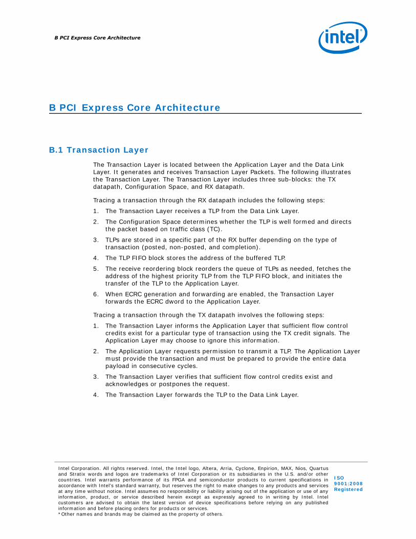
B PCI Express Core Architecture
B.1 Transaction Layer
The Transaction Layer is located between the Application Layer and the Data LinkLayer. It generates and receives Transaction Layer Packets. The following illustratesthe Transaction Layer. The Transaction Layer includes three sub-blocks: the TXdatapath, Configuration Space, and RX datapath.
Tracing a transaction through the RX datapath includes the following steps:
1. The Transaction Layer receives a TLP from the Data Link Layer.
2. The Configuration Space determines whether the TLP is well formed and directsthe packet based on traffic class (TC).
3. TLPs are stored in a specific part of the RX buffer depending on the type oftransaction (posted, non-posted, and completion).
4. The TLP FIFO block stores the address of the buffered TLP.
5. The receive reordering block reorders the queue of TLPs as needed, fetches theaddress of the highest priority TLP from the TLP FIFO block, and initiates thetransfer of the TLP to the Application Layer.
6. When ECRC generation and forwarding are enabled, the Transaction Layerforwards the ECRC dword to the Application Layer.
Tracing a transaction through the TX datapath involves the following steps:
1. The Transaction Layer informs the Application Layer that sufficient flow controlcredits exist for a particular type of transaction using the TX credit signals. TheApplication Layer may choose to ignore this information.
2. The Application Layer requests permission to transmit a TLP. The Application Layermust provide the transaction and must be prepared to provide the entire datapayload in consecutive cycles.
3. The Transaction Layer verifies that sufficient flow control credits exist andacknowledges or postpones the request.
4. The Transaction Layer forwards the TLP to the Data Link Layer.
B PCI Express Core Architecture
Intel Corporation. All rights reserved. Intel, the Intel logo, Altera, Arria, Cyclone, Enpirion, MAX, Nios, Quartusand Stratix words and logos are trademarks of Intel Corporation or its subsidiaries in the U.S. and/or othercountries. Intel warrants performance of its FPGA and semiconductor products to current specifications inaccordance with Intel's standard warranty, but reserves the right to make changes to any products and servicesat any time without notice. Intel assumes no responsibility or liability arising out of the application or use of anyinformation, product, or service described herein except as expressly agreed to in writing by Intel. Intelcustomers are advised to obtain the latest version of device specifications before relying on any publishedinformation and before placing orders for products or services.*Other names and brands may be claimed as the property of others.
ISO9001:2008Registered

Figure 79. Architecture of the Transaction Layer: Dedicated Receive Buffer
Transaction Layer TX Datapath
Transaction Layer RX Datapath
Avalon-STRX Control
Configuration Space
TLPs to theData Link Layer
TLPs from the Data Link Layer
Avalon-ST RX Data
Avalon-STTX Data
to Application Layer
ConfigurationRequests
Reordering
RX Buffer
Posted & Completion
Non-Posted
Flow Control Update
Transaction Layer Packet FIFO
WidthAdapter( <256
bits)
PacketAlignment TX
Control
RXControl
TX Flow Control
B.2 Data Link Layer
The Data Link Layer is located between the Transaction Layer and the Physical Layer.It maintains packet integrity and communicates (by DLL packet transmission) at thePCI Express link level.
The DLL implements the following functions:
• Link management through the reception and transmission of DLL packets (DLLP),which are used for the following functions:
— Power management of DLLP reception and transmission
— To transmit and receive ACK/NAK packets
— Data integrity through generation and checking of CRCs for TLPs and DLLPs
— TLP retransmission in case of NAK DLLP reception or replay timeout, using theretry (replay) buffer
— Management of the retry buffer
— Link retraining requests in case of error through the Link Training and StatusState Machine (LTSSM) of the Physical Layer
B PCI Express Core Architecture
Intel® Stratix® 10 Avalon-ST Interface for PCIe Solutions User Guide155

Figure 80. Data Link LayerTo Transaction Layer
Tx Transaction LayerPacket Description & Data Transaction Layer
Packet Generator
Retry Buffer
To Physical Layer
Tx Packets
Ack/NackPackets
RX Datapath
TX Datapath
Rx Packets
DLLPChecker
Transaction LayerPacket Checker
DLLPGenerator
Tx Arbitration
Data Link Controland Management
State Machine
Control& StatusConfiguration Space
Tx Flow Control Credit Information
Rx Flow Control Credit Information
Rx Transation LayerPacket Description & Data
PowerManagement
Function
Note:(1) The L0s (Standby) or L1 (Low Power Standby) states are not supported. The DLL has the following sub-blocks:
• Data Link Control and Management State Machine—This state machine connects toboth the Physical Layer’s LTSSM state machine and the Transaction Layer. Itinitializes the link and flow control credits and reports status to the TransactionLayer.
• Power Management—This function handles the handshake to enter low powermode. Such a transition is based on register values in the Configuration Space andreceived Power Management (PM) DLLPs. None of Stratix 10 Hard IP for PCIe IPcore variants support low power modes.
• Data Link Layer Packet Generator and Checker—This block is associated with theDLLP’s 16-bit CRC and maintains the integrity of transmitted packets.
• Transaction Layer Packet Generator—This block generates transmit packets,including a sequence number and a 32-bit Link CRC (LCRC). The packets are alsosent to the retry buffer for internal storage. In retry mode, the TLP generatorreceives the packets from the retry buffer and generates the CRC for the transmitpacket.
• Retry Buffer—The retry buffer stores TLPs and retransmits all unacknowledgedpackets in the case of NAK DLLP reception. In case of ACK DLLP reception, theretry buffer discards all acknowledged packets.
B PCI Express Core Architecture
Intel® Stratix® 10 Avalon-ST Interface for PCIe Solutions User Guide156

• ACK/NAK Packets—The ACK/NAK block handles ACK/NAK DLLPs and generates thesequence number of transmitted packets.
• Transaction Layer Packet Checker—This block checks the integrity of the receivedTLP and generates a request for transmission of an ACK/NAK DLLP.
• TX Arbitration—This block arbitrates transactions, prioritizing in the followingorder:
— Initialize FC Data Link Layer packet
— ACK/NAK DLLP (high priority)
— Update FC DLLP (high priority)
— PM DLLP
— Retry buffer TLP
— TLP
— Update FC DLLP (low priority)
— ACK/NAK FC DLLP (low priority)
B.3 Physical Layer
The Physical Layer is the lowest level of the PCI Express protocol stack. It is the layerclosest to the serial link. It encodes and transmits packets across a link and acceptsand decodes received packets. The Physical Layer connects to the link through ahigh-speed SERDES interface running at 2.5 Gbps for Gen1 implementations, at 2.5 or5.0 Gbps for Gen2 implementations, and at 2.5, 5.0 or 8.0 Gbps for Gen3implementations.
The Physical Layer is responsible for the following actions:
• Training the link
• Scrambling/descrambling and 8B/10B encoding/decoding for 2.5 Gbps (Gen1),5.0 Gbps (Gen2), or 128b/130b encoding/decoding of 8.0 Gbps (Gen3) per lane
• Serializing and deserializing data
• Equalization (Gen3)
• Operating the PIPE 3.0 Interface
• Implementing auto speed negotiation (Gen2 and Gen3)
• Transmitting and decoding the training sequence
• Providing hardware autonomous speed control
• Implementing auto lane reversal
The Physical Layer is subdivided by the PIPE Interface Specification into two layers(bracketed horizontally in above figure):
• PHYMAC—The MAC layer includes the LTSSM and the scrambling/descrambling.byte reordering, and multilane deskew functions.
• PHY Layer—The PHY layer includes the 8B/10B encode and decode functions forGen1 and Gen2. It includes 128b/130b encode and decode functions for Gen3.The PHY also includes elastic buffering and serialization/deserialization functions.
B PCI Express Core Architecture
Intel® Stratix® 10 Avalon-ST Interface for PCIe Solutions User Guide157

The Physical Layer integrates both digital and analog elements. Intel designed thePIPE interface to separate the PHYMAC from the PHY. The Stratix 10 Hard IP for PCIExpress complies with the PIPE interface specification.
Note: The internal PIPE interface is visible for simulation. It is not available for debugging inhardware using a logic analyzer such as SignalTap® II. If you try to connect SignalTapII to this interface you will not be able to compile your design.
B PCI Express Core Architecture
Intel® Stratix® 10 Avalon-ST Interface for PCIe Solutions User Guide158

Figure 81. Physical Layer Architecture
TX+ / TX-
TX+ / TX-
Descrambler 8B/10BDecoder
128b/130bEncoder/Decoder
Lane n
RX+ / RX-ElasticBuffer
LTSSM State Machine
SKIPGeneration
Control & StatusRX MAC
Gen1, Gen2
Gen1, Gen2
Gen1, Gen2
Gen1, Gen2
Gen3
Gen3
TX MAC
Link S
erial
izer
for a
n x8 L
inkTX Packets
Dev
ice T
rans
ceive
r (pe
r Lan
e) w
ith 2.
5, 5.0
, or 8
Gbp
s SER
DES &
PLL
Descrambler
Lane 0RX+ / RX-
PIPEInterface
Byte
Reor
der &
Mult
ilane
Des
kew
Link S
erial
izer f
or an
x8 Li
nk
RX Packets
TransmitData Path
ReceiveData Path
PHYMAC Layer PHY Layer
To LinkTo Data Link Layer
8B10BDecoder
128b/130bEncoder/Decoder
ElasticBuffer
Lane 0(or) 128b/130b
Encoder/Decoder
Scrambler 8B/10BEncoder
Gen3
Lane n(or) 128b/130b
Encoder/Decoder
8B/10BEncoder
Gen3
Scrambler
The PHYMAC block comprises four main sub-blocks:
• MAC Lane—Both the RX and the TX path use this block.
— On the RX side, the block decodes the Physical Layer packet and reports to theLTSSM the type and number of TS1/TS2 ordered sets received.
— On the TX side, the block multiplexes data from the DLL and the Ordered Setand SKP sub-block (LTSTX). It also adds lane specific information, includingthe lane number and the force PAD value when the LTSSM disables the laneduring initialization.
• LTSSM—This block implements the LTSSM and logic that tracks TX and RX trainingsequences on each lane.
• For transmission, it interacts with each MAC lane sub-block and with the LTSTXsub-block by asserting both global and per-lane control bits to generate specificPhysical Layer packets.
— On the receive path, it receives the Physical Layer packets reported by eachMAC lane sub-block. It also enables the multilane deskew block. This blockreports the Physical Layer status to higher layers.
— LTSTX (Ordered Set and SKP Generation)—This sub-block generates thePhysical Layer packet. It receives control signals from the LTSSM block andgenerates Physical Layer packet for each lane. It generates the same PhysicalLayer Packet for all lanes and PAD symbols for the link or lane number in thecorresponding TS1/TS2 fields. The block also handles the receiver detectionoperation to the PCS sub-layer by asserting predefined PIPE signals andwaiting for the result. It also generates a SKP Ordered Set at every predefinedtimeslot and interacts with the TX alignment block to prevent the insertion of aSKP Ordered Set in the middle of packet.
— Deskew—This sub-block performs the multilane deskew function and the RXalignment between the initialized lanes and the datapath. The multilanedeskew implements an eight-word FIFO buffer for each lane to store symbols.Each symbol includes eight data bits, one disparity bit, and one control bit.The FIFO discards the FTS, COM, and SKP symbols and replaces PAD and IDLwith D0.0 data. When all eight FIFOs contain data, a read can occur. When themultilane lane deskew block is first enabled, each FIFO begins writing after thefirst COM is detected. If all lanes have not detected a COM symbol after sevenclock cycles, they are reset and the resynchronization process restarts, or elsethe RX alignment function recreates a 64-bit data word which is sent to theDLL.
B PCI Express Core Architecture
Intel® Stratix® 10 Avalon-ST Interface for PCIe Solutions User Guide159

C TX Credit Adjustment Sample CodeThis sample Verilog HDL code computes the available credits for non-posted TLPs. Itprovides the updated credit information from the remote device on the tx_nph_cdtsand tx_npd_cdts buses. The tx_nph_cdts and tx_npd_cdts buses drive theactual available credit space in the link partner's RX buffer. The actual credit space isdifficult to use due to the EMIB (Embedded Multi-die Interconnect Bridge) latency.
The following Verilog RTL restores the credit limit for non-posted TLPs that can beused by application logic before it sends a TLP.
module nph_credit_limit_gen ( input clk, input rst_n, input [7:0] tx_nph_cdts, input tx_hdr_cdts_consumed, input [1:0] tx_cdts_type, output [7:0] tx_nph_cdts_limit); reg tx_nph_credit_consume_1r; reg tx_nph_credit_consume_2r; reg [7:0] tx_nph_credit_consume_count_hip_3r; always @(posedge clk) begin if (!rst_n) begin tx_nph_credit_consume_1r <= 1'b0; tx_nph_credit_consume_2r <= 1'b0; tx_nph_credit_consume_count_hip <= 8'h0;
end else begin tx_nph_credit_consume_1r <= (tx_cdts_type == 2'b01) ? tx_hdr_cdts_consumed : 1'b0; tx_nph_credit_consume_2r <= tx_nph_credit_consume_1r; tx_nph_credit_consume_count_hip_3r <= tx_nph_credit_consume_count_hip_3r + tx_nph_credit_consume_2r; end end assign tx_nph_cdts_limit = tx_nph_cdts + tx_nph_credit_consume_count_hip_3r; endmodule
The following pseudo-code explains the Verilog RTL above.
// reset credit_consume_count initiallytx_nph_credit_consume_count = 0; tx_nph_credit_consume_count_hip = 0;
if (tx_nph_credit_limit_count – (tx_nph_credit_consume_count + tx_nph_credit_required) <= (2^8)/2) { send NPH packet tx_nph_credit_consume_count += tx_nph_credit_required;}
where
C TX Credit Adjustment Sample Code
Intel Corporation. All rights reserved. Intel, the Intel logo, Altera, Arria, Cyclone, Enpirion, MAX, Nios, Quartusand Stratix words and logos are trademarks of Intel Corporation or its subsidiaries in the U.S. and/or othercountries. Intel warrants performance of its FPGA and semiconductor products to current specifications inaccordance with Intel's standard warranty, but reserves the right to make changes to any products and servicesat any time without notice. Intel assumes no responsibility or liability arising out of the application or use of anyinformation, product, or service described herein except as expressly agreed to in writing by Intel. Intelcustomers are advised to obtain the latest version of device specifications before relying on any publishedinformation and before placing orders for products or services.*Other names and brands may be claimed as the property of others.
ISO9001:2008Registered

tx_nph_credit_required: the number of credits required to send given NP TLP. For NP, tx_nph_credit_required is 1.tx_nph_credit_consume_count_hip += (tx_cdts_type == "01") ? tx_hdr_cdts_consumed : 1'b0;tx_nph_credit_consume_count_hip_delayed : three pld_clk cycle delayed tx_nph_credit_consume_count_hiptx_nph_credit_limit_count = tx_nph_cdts + tx_nph_credit_consume_count_hip_delayed;
C TX Credit Adjustment Sample Code
Intel® Stratix® 10 Avalon-ST Interface for PCIe Solutions User Guide161

D Stratix 10 Avalon-ST Interface for PCIe Solutions UserGuide Archive
If an IP core version is not listed, the user guide for the previous IP core version applies.
IP Core Version User Guide
16.1 Stratix 10 EditionBeta Beta
Stratix 10 Avalon-ST Interface for PCIe Solutions User Guide
D Stratix 10 Avalon-ST Interface for PCIe Solutions User Guide Archive
Intel Corporation. All rights reserved. Intel, the Intel logo, Altera, Arria, Cyclone, Enpirion, MAX, Nios, Quartusand Stratix words and logos are trademarks of Intel Corporation or its subsidiaries in the U.S. and/or othercountries. Intel warrants performance of its FPGA and semiconductor products to current specifications inaccordance with Intel's standard warranty, but reserves the right to make changes to any products and servicesat any time without notice. Intel assumes no responsibility or liability arising out of the application or use of anyinformation, product, or service described herein except as expressly agreed to in writing by Intel. Intelcustomers are advised to obtain the latest version of device specifications before relying on any publishedinformation and before placing orders for products or services.*Other names and brands may be claimed as the property of others.
ISO9001:2008Registered

E Document Revision History
Date Version Changes
May 2017 Quartus PrimePro v17.1 Stratix10 ES Editions
Software
Made the following changes to the IP core:• Added support for the H-Tile transceiver including example designs
available in the installation directory.• Added support for a Gen3x16 simulation testbench model that you can
use in an Avery testbench.Made the following changes to the user guide:• Added definitions for Advance, Preliminary, and Final timing models.• Added Testbench and Design Example for the Avalon-ST Interface
chapter.• Added figures showing the connections between the Avalon-ST and
user application and between Stratix 10 Hard IP for PCI Express IPCore, system interfaces, and the user application.
• Revised Generation discussion to match theThe Quartus Prime Pro v17.1 Stratix 10 ES Editions Software designflow.
• Changed TX credit interface pseudo code.tx_nph_credit_consume_count_hip_delayed is 3 pld_clkcycle delayed, not 2.
October 2016 Quartus PrimePro – Stratix 10
Edition Beta
Initial release
E Document Revision History
Intel Corporation. All rights reserved. Intel, the Intel logo, Altera, Arria, Cyclone, Enpirion, MAX, Nios, Quartusand Stratix words and logos are trademarks of Intel Corporation or its subsidiaries in the U.S. and/or othercountries. Intel warrants performance of its FPGA and semiconductor products to current specifications inaccordance with Intel's standard warranty, but reserves the right to make changes to any products and servicesat any time without notice. Intel assumes no responsibility or liability arising out of the application or use of anyinformation, product, or service described herein except as expressly agreed to in writing by Intel. Intelcustomers are advised to obtain the latest version of device specifications before relying on any publishedinformation and before placing orders for products or services.*Other names and brands may be claimed as the property of others.
ISO9001:2008Registered


