
ISM4334x Product Specification
DOC-DS-20072-3.2 Confidential Inventek Systems Page 1
INVENTEK SYSTEMS ISM4334X-L77
Embedded SiP Module 802.11 a/b/g/n Bluetooth 4.0 & NFC Data Sheet

ISM4334x Product Specification
DOC-DS-20072-3.2 Confidential Inventek Systems Page 2
Table of Contents
1 PART NUMBER DETAIL DESCRIPTION .......................................................................... 3 1.1 Ordering Information ...................................................................................................... 3
2 OVERVIEW ........................................................................................................................... 3 3 FEATURES ............................................................................................................................ 4
3.1 Limitations ...................................................................................................................... 5
4 COMPLEMENTARY DOCUMENTATION ........................................................................ 5 4.1 Inventek Systems ............................................................................................................ 5
5 BLOCK DIAGRAM ............................................................................................................... 6 6 HOST INTERFACES ............................................................................................................. 6
6.1 UART Interface .............................................................................................................. 6 6.2 NFC Host Interfaces (ISM43341 only)........................................................................... 8
7 ELECTRICAL SPECIFICATIONS ....................................................................................... 8
7.1 Absolute Maximum Ratings ........................................................................................... 8 7.2 Environmental Ratings.................................................................................................... 9
7.3 Recommended Operating Conditions and DC Characteristics ....................................... 9 8 RF SPECIFICATIONS ........................................................................................................... 9
8.1 Bluetooth RF Specifications ........................................................................................... 9
8.2 WLAN RF Specifications ............................................................................................. 10
8.3 Environmental Specifications ....................................................................................... 13 9 PIN OUT AND DESCRIPTIONS ........................................................................................ 14
9.1 Module Pin-Out (1 of 2) ............................................................................................... 14
9.2 Module Pin-Out (2 of 2) ............................................................................................... 15 9.3 Recommended PCB Footprint (Bottom View) ............................................................. 16 9.4 Recommended PCB Footprint (Top View) .................................................................. 17
9.5 Detailed Pin Description ............................................................................................... 18 10 Product Compliance Considerations ..................................................................................... 20 11 Reflow Profile ....................................................................................................................... 21 12 Packaging Information .......................................................................................................... 22
12.1 MSL Level / Storage Condition .................................................................................... 22
12.2 Device baking requirements prior to assembly ............................................................. 23
13 REVISION CONTROL ........................................................................................................ 23
14 CONTACT INFORMATION ............................................................................................... 23

ISM4334x Product Specification
DOC-DS-20072-3.2 Confidential Inventek Systems Page 3
1 PART NUMBER DETAIL DESCRIPTION
1.1 Ordering Information
Device Description Ordering Number ISM43341-L77 2.4/5G Wi-Fi, Bluetooth, NFC
SiP Module ISM43341-L77
ISM43340-L77 2.4/5G Wi-Fi, Bluetooth SiP Module
ISM43340-L77
ISM43341-SDIO-EVB or ISM43340
SDIO Evaluation Board ISM43341-SDIO-EVB
2 OVERVIEW The Inventek ISM4443X single-chip quad-radio device provides the highest level of integration for a wireless system, with integrated dual band (2.4 GHz/ 5 GHz) IEEE 802.11 a/b/g and single-stream IEEE 802.11n MAC/baseband/radio, Bluetooth 4.0. The ISM43341 also integrates a low power NFC controller. The ISM4443X includes integrated power amplifiers, LNAs and T/R switches for the 2.4 GHz and 5 GHz WLAN bands, greatly reducing the external part count, PCB footprint, and cost of the solution. It provides a small form-factor solution with minimal external components to drive down cost for mass volumes and allows for handheld device flexibility in size, form and function. Comprehensive power management circuitry and software ensure the system can meet the needs of high mobile devices that require minimal power consumption and reliable operations.
The ISM4443X is compatible with the Bluetooth Low Energy operating mode, which provides a dramatic reduction in the power consumption of the Bluetooth radio and baseband. The primary application for this mode is to provide support for low data rate devices, such as sensors and remote controls.
The ISM4443X implements the highly sophisticated Enhanced Collaborative Coexistence algorithms and hardware mechanisms, allowing for an extremely collaborative Bluetooth coexistence scheme along with coexistence support for external radios such as cellular and LTE, GPS, and Ultra-Wideband. For the WLAN section, host interface is a SDIO v2.0 interface. An independent, high-speed UART is provided for the Bluetooth host interface. Separate independent interfaces (I²C-compatible, SPI and UART) for NFC are also provided.
ISM4334x Product Specification
DOC-DS-20072-3.2 Confidential Inventek Systems Page 4
3 FEATURES
The ISM4443X supports the following WLAN, Bluetooth functions:
Dual-band 2.4 GHz and 5 GHz IEEE 802.11 a/b/g/n
Single-stream IEEE 802.11n support for 20 MHz and 40 MHz channels provides PHY
layer rates up to 150 Mbps for typical upper-layer throughput in excess of 90 Mbps.
Supports a single 2.4 GHz antenna shared between WLAN and Bluetooth
IEEE 802.11a/b/g/n dual-band radio with internal Power Amplifiers, LNAs and T/R
switches
OneDriver™ software architecture for easy migration from existing embedded WLAN
and Bluetooth devices as well as future devices.
Bluetooth v4.0 with integrated Class 1 PA
Concurrent Bluetooth, NFC and WLAN operation
On-chip WLAN driver execution capable of supporting IEEE 802.11 functionality
Single and dual-antenna support
WLAN host interface :
o SDIO v2.0, including default and high-speed timing.
BT host digital interface (can be used concurrently with above interface):
o UART (up to 4 Mbps)
ECI – enhanced coexistence support, ability to coordinate BT SCO transmissions
around WLAN receives
I²S/PCM for BT audio
HCI high-speed UART (H4, H4 +, H5) transport support
Bluetooth SmartAudio® technology improves voice and music quality to headsets
Bluetooth low power inquiry and page scan
Bluetooth Low Energy (BLE) support
Bluetooth Packet Loss Concealment (PLC)
Bluetooth Wide Band Speech (WBS)
The BBC supports all Bluetooth 4.0 features, with the following benefits:
Dual-mode classic Bluetooth and classic Low Energy (BT and BLE) operation.
Low Energy Physical Layer
Low Energy Link Layer
Enhancements to HCI for Low Energy
Low Energy Direct Test mode
AES encryption The ISM43341 supports the following NFC features:
Support for the ISO/IEC 18092, ISO/IEC 21481, ISO/IEC 14443 Types A, B and B’,
Japanese Industrial Standard (JIS) (X) 6319-4 and ISO/IEC 15693 standards
No active components required for antenna or field-power conditioning
Individual byte framing

ISM4334x Product Specification
DOC-DS-20072-3.2 Confidential Inventek Systems Page 5
Hardware-based collision detection and modulation controls
Reader/Writer (R/W) mode
Active and Passive Peer-to-Peer (P2P) mode
Tag/Card Emulation mode:
o Support for battery-enabled card emulation mode
o Support for two levels of “residual” battery-assisted card emulation mode
o Support for “battery-off” card emulation mode (completely powered from the field)
Dual Signal Wire Protocol (SWP) interfaces:
o SWP_0 with platform power management unit (PMU) power switching to a UICC
SIM card
o SWP_1 for embedded secure element or a second UICC SIM card
Supports Application ID (AID) routing between a reader and secure element(s)
Ability to recover card emulation personality data
Internal low-power oscillator for periodic wake-up and mode switch operation
Low-Power Target Detection mode for extremely low average current consumption
(“sniff mode”)
NFC Forum NFC Controller Interface (NCI) for the host interface
3.1 Limitations
Inventek Systems products are not authorized for use in safety-critical applications (such as life support) where a failure of the Inventek Systems product would reasonably be expected to cause severe personal injury or death.
4 COMPLEMENTARY DOCUMENTATION
4.1 Inventek Systems
Evaluation Board
o SDIO Evaluation Board Specification
o EVB User’s Guide
o Drivers under NDA
o Design Guidelines
ISM4334x Product Specification
DOC-DS-20072-3.2 Confidential Inventek Systems Page 6
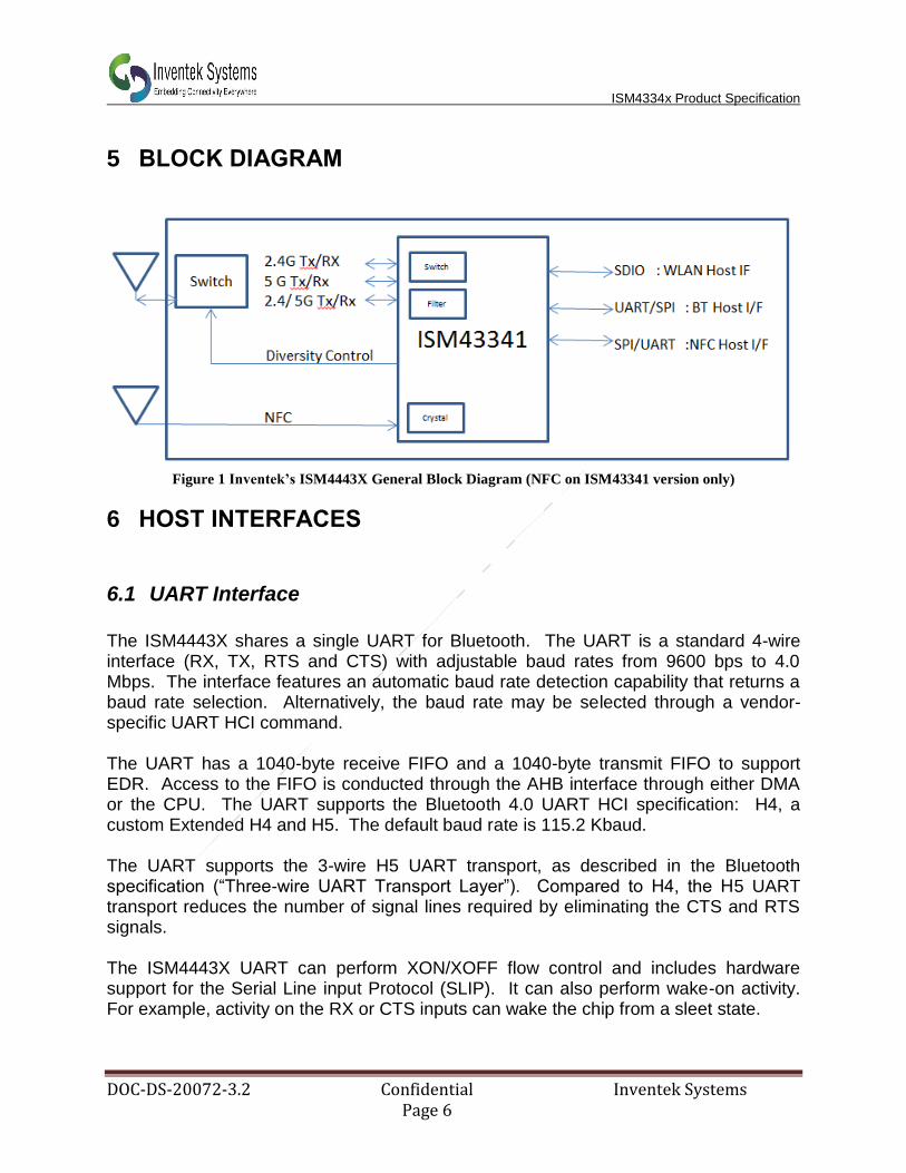
5 BLOCK DIAGRAM
Figure 1 Inventek’s ISM4443X General Block Diagram (NFC on ISM43341 version only)
6 HOST INTERFACES
6.1 UART Interface
The ISM4443X shares a single UART for Bluetooth. The UART is a standard 4-wire interface (RX, TX, RTS and CTS) with adjustable baud rates from 9600 bps to 4.0 Mbps. The interface features an automatic baud rate detection capability that returns a baud rate selection. Alternatively, the baud rate may be selected through a vendor-specific UART HCI command. The UART has a 1040-byte receive FIFO and a 1040-byte transmit FIFO to support EDR. Access to the FIFO is conducted through the AHB interface through either DMA or the CPU. The UART supports the Bluetooth 4.0 UART HCI specification: H4, a custom Extended H4 and H5. The default baud rate is 115.2 Kbaud. The UART supports the 3-wire H5 UART transport, as described in the Bluetooth specification (“Three-wire UART Transport Layer”). Compared to H4, the H5 UART transport reduces the number of signal lines required by eliminating the CTS and RTS signals. The ISM4443X UART can perform XON/XOFF flow control and includes hardware support for the Serial Line input Protocol (SLIP). It can also perform wake-on activity. For example, activity on the RX or CTS inputs can wake the chip from a sleet state.

ISM4334x Product Specification
DOC-DS-20072-3.2 Confidential Inventek Systems Page 7
Normally, the UART baud rate is set by a configuration record downloaded after device reset, or by automatic baud rate detection, and the host does not need to adjust the baud rate. Support for changing the baud rate during normal HCI UART operation is included through a vendor-specific command that allows the host to adjust the contents of the baud rate registers. The ISM4443X UARTs operate correctly with the host UART as long as the combined baud rate error of the two devices is within ±2% (see Table 12).
Desired Rate Actual Rate Error (%)
4000000 4000000 0.00
3692000 3692308 0.01
3000000 3000000 0.00
2000000 2000000 0.00
1500000 1500000 0.00
1444444 1454544 0.70
921600 923077 0.16
460800 461538 0.16
230400 230796 0.17
115200 115385 0.16
57600 57692 0.16
38400 38400 0.00
28800 28846 0.16
19200 19200 0.00
14400 14423 0.16
9600 9600 0.00
Table 1: Example of Common Baud Rates

ISM4334x Product Specification
DOC-DS-20072-3.2 Confidential Inventek Systems Page 8
6.2 NFC Host Interfaces (ISM43341 only)
The ISM43341 supports UART, I²C-compatible BSC, and SPI for the host interface physical transport layer. The host interface type is selected upon power-up boot, depending upon the state of the NFC_SPI_INT pin.
NFC_SPI_INT pulled low – The UART interface will be selected
NFC_SPI_INT pulled high – The I²C-compatible BSC slave interface will be selected
NFC_SPI_INT floating – The SPI interface will be selected. After boot, the NFC_SPI_INT signal will function as the SPI interrupt output. During power-up book, the external host must leave this pin floating, as in the case of the tri-state or input pin. The external host must also ignore interrupts from this signal for a period of 10 milliseconds after boot-up. The NFC host interface pins are multiplexed onto shared signals as defined in Table 2.
UART BSC SPI
NFC_CTS I2C_REQ SPI_CS
NFC_RTS I2C_SCL SPI_MISO
NFC_URX - SPI_CLK
NFC_UTX I2C_SDA SPI-MOSI
Pull low Pull high NFC_SPI_INT
Table 2: NFC Host Interface Multiplexing
7 ELECTRICAL SPECIFICATIONS
7.1 Absolute Maximum Ratings
Caution! The absolute maximum ratings in Table 28 indicate levels where permanent damage to the device can occur, even if these limits are exceeded for only a brief duration. Functional operation is not guaranteed under these conditions. Operation at absolute maximum conditions for extended periods can adversely affect long-term reliability of the device.
Rating Symbol Value Unit
DC supply for VBAT and PA driver supply VBAT -0.5 to +6.0 V
DC supply voltage for digital I/O VIO -0.5 to 3.9 V
Table 3: Absolute Maximum Ratings
ISM4334x Product Specification
DOC-DS-20072-3.2 Confidential Inventek Systems Page 9
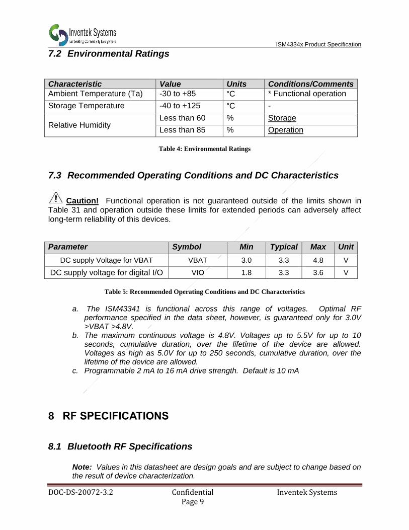
7.2 Environmental Ratings
Characteristic Value Units Conditions/Comments
Ambient Temperature (Ta) -30 to +85 °C * Functional operation
Storage Temperature -40 to +125 °C -
Relative Humidity Less than 60 % Storage
Less than 85 % Operation
Table 4: Environmental Ratings
7.3 Recommended Operating Conditions and DC Characteristics
Caution! Functional operation is not guaranteed outside of the limits shown in Table 31 and operation outside these limits for extended periods can adversely affect long-term reliability of this devices.
Parameter Symbol Min Typical Max Unit
DC supply Voltage for VBAT VBAT 3.0 3.3 4.8 V
DC supply voltage for digital I/O VIO 1.8 3.3 3.6 V
Table 5: Recommended Operating Conditions and DC Characteristics
a. The ISM43341 is functional across this range of voltages. Optimal RF
performance specified in the data sheet, however, is guaranteed only for 3.0V >VBAT >4.8V.
b. The maximum continuous voltage is 4.8V. Voltages up to 5.5V for up to 10 seconds, cumulative duration, over the lifetime of the device are allowed. Voltages as high as 5.0V for up to 250 seconds, cumulative duration, over the lifetime of the device are allowed.
c. Programmable 2 mA to 16 mA drive strength. Default is 10 mA
8 RF SPECIFICATIONS
8.1 Bluetooth RF Specifications
Note: Values in this datasheet are design goals and are subject to change based on the result of device characterization.

ISM4334x Product Specification
DOC-DS-20072-3.2 Confidential Inventek Systems Page 10
Unless otherwise stated, limit values apply for the conditions specified in Tabel 29: “Environmental Ratings” on page 117 and table 31: “Recommended Operating Conditions and DC Characteristics” on page 118. Typical values apply for the following conditions:
VBAT = 3.6V
Ambient temperature +25°Cͨ
Parameter Conditions Min Typical Max Unit
Note: The specifications in this table are measured at the Chip port output unless otherwise specified:
General
Frequency Range - 2402 - 2480 MHz
RX sensitivity
GFSK, 0.1% BER, 1 Mbps
- -93.5 - dBm
π/4-DQPSK,
0.01% BER, 2 Mbps
- -95.5 - dBm
8-DPSK, 0.01% BER, 3 Mbps
- -89.5 - dBm
Input IP3 - -16 - - dBm
Maximum input at antenna - - - -20 dBm
Table 6: Bluetooth Receiver RF Specifications
Parameter Conditions Min Typical Max Unit
General
Frequency Range 2402 - 2480 MHz
Basic rate (GFSK) Tx power at Bluetooth
- 10.0 12.0 - dBm
QPSK Tx Power at Bluetooth 7.0 9.0 - dBm
8PSK Tx Power at Bluetooth 7.0 9.0 - dBm
Power control step 2 4 6 dB
Table 7: Bluetooth Transmitter RF Specifications
8.2 WLAN RF Specifications
ISM4334x Product Specification
DOC-DS-20072-3.2 Confidential Inventek Systems Page 11
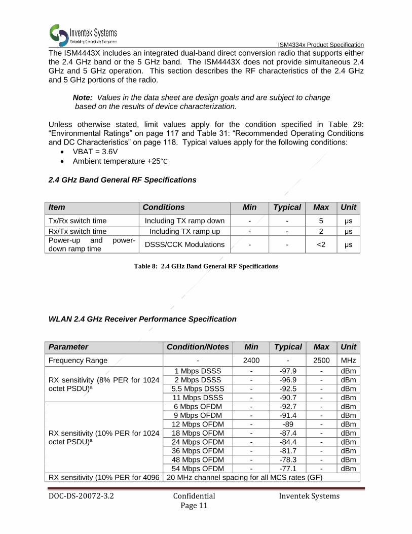
The ISM4443X includes an integrated dual-band direct conversion radio that supports either the 2.4 GHz band or the 5 GHz band. The ISM4443X does not provide simultaneous 2.4 GHz and 5 GHz operation. This section describes the RF characteristics of the 2.4 GHz and 5 GHz portions of the radio.
Note: Values in the data sheet are design goals and are subject to change based on the results of device characterization.
Unless otherwise stated, limit values apply for the condition specified in Table 29: “Environmental Ratings” on page 117 and Table 31: “Recommended Operating Conditions and DC Characteristics” on page 118. Typical values apply for the following conditions:
VBAT = 3.6V
Ambient temperature +25°C
2.4 GHz Band General RF Specifications
Item Conditions Min Typical Max Unit
Tx/Rx switch time Including TX ramp down - - 5 μs
Rx/Tx switch time Including TX ramp up - - 2 μs
Power-up and power-down ramp time
DSSS/CCK Modulations - - <2 μs
Table 8: 2.4 GHz Band General RF Specifications
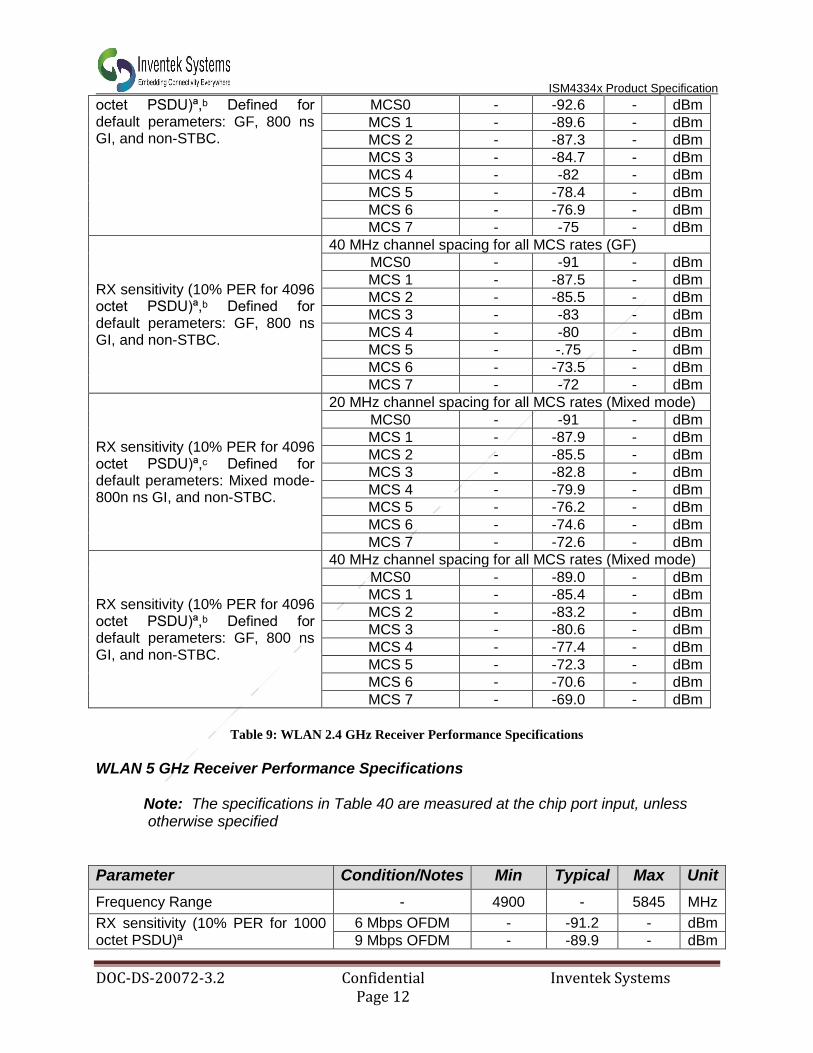
WLAN 2.4 GHz Receiver Performance Specification
Parameter Condition/Notes Min Typical Max Unit
Frequency Range - 2400 - 2500 MHz
RX sensitivity (8% PER for 1024 octet PSDU)ª
1 Mbps DSSS - -97.9 - dBm
2 Mbps DSSS - -96.9 - dBm
5.5 Mbps DSSS - -92.5 - dBm
11 Mbps DSSS - -90.7 - dBm
RX sensitivity (10% PER for 1024 octet PSDU)ª
6 Mbps OFDM - -92.7 - dBm
9 Mbps OFDM - -91.4 - dBm
12 Mbps OFDM - -89 - dBm
18 Mbps OFDM - -87.4 - dBm
24 Mbps OFDM - -84.4 - dBm
36 Mbps OFDM - -81.7 - dBm
48 Mbps OFDM - -78.3 - dBm
54 Mbps OFDM - -77.1 - dBm
RX sensitivity (10% PER for 4096 20 MHz channel spacing for all MCS rates (GF)
ISM4334x Product Specification
DOC-DS-20072-3.2 Confidential Inventek Systems Page 12
octet PSDU)ª,ᵇ Defined for default perameters: GF, 800 ns GI, and non-STBC.
MCS0 - -92.6 - dBm
MCS 1 - -89.6 - dBm
MCS 2 - -87.3 - dBm
MCS 3 - -84.7 - dBm
MCS 4 - -82 - dBm
MCS 5 - -78.4 - dBm
MCS 6 - -76.9 - dBm
MCS 7 - -75 - dBm
RX sensitivity (10% PER for 4096 octet PSDU)ª,ᵇ Defined for default perameters: GF, 800 ns GI, and non-STBC.
40 MHz channel spacing for all MCS rates (GF)
MCS0 - -91 - dBm
MCS 1 - -87.5 - dBm
MCS 2 - -85.5 - dBm
MCS 3 - -83 - dBm
MCS 4 - -80 - dBm
MCS 5 - -.75 - dBm
MCS 6 - -73.5 - dBm
MCS 7 - -72 - dBm
RX sensitivity (10% PER for 4096 octet PSDU)ª,ᶜ Defined for default perameters: Mixed mode- 800n ns GI, and non-STBC.
20 MHz channel spacing for all MCS rates (Mixed mode)
MCS0 - -91 - dBm
MCS 1 - -87.9 - dBm
MCS 2 - -85.5 - dBm
MCS 3 - -82.8 - dBm
MCS 4 - -79.9 - dBm
MCS 5 - -76.2 - dBm
MCS 6 - -74.6 - dBm
MCS 7 - -72.6 - dBm
RX sensitivity (10% PER for 4096 octet PSDU)ª,ᵇ Defined for default perameters: GF, 800 ns GI, and non-STBC.
40 MHz channel spacing for all MCS rates (Mixed mode)
MCS0 - -89.0 - dBm
MCS 1 - -85.4 - dBm
MCS 2 - -83.2 - dBm
MCS 3 - -80.6 - dBm
MCS 4 - -77.4 - dBm
MCS 5 - -72.3 - dBm
MCS 6 - -70.6 - dBm
MCS 7 - -69.0 - dBm
Table 9: WLAN 2.4 GHz Receiver Performance Specifications
WLAN 5 GHz Receiver Performance Specifications
Note: The specifications in Table 40 are measured at the chip port input, unless otherwise specified
Parameter Condition/Notes Min Typical Max Unit
Frequency Range - 4900 - 5845 MHz
RX sensitivity (10% PER for 1000 octet PSDU)ª
6 Mbps OFDM - -91.2 - dBm
9 Mbps OFDM - -89.9 - dBm

ISM4334x Product Specification
DOC-DS-20072-3.2 Confidential Inventek Systems Page 13
12 Mbps OFDM - -87.5 - dBm
18 Mbps OFDM - -85.9 - dBm
24 Mbps OFDM - -82.9 - dBm
36 Mbps OFDM - -80.2 - dBm
48 Mbps OFDM - -76.8 - dBm
54 Mbps OFDM - -75.6 - dBm
RX sensitivity (10% PER for 4096 octet PSDU)ª Defined for default perameters: GF, 800 ns GI, and non-STBC.
20 MHz channel spacing for all MCS rates (GF)
MCS0 - -91.1 - dBm
MCS 1 - -88.1 - dBm
MCS 2 - -85.8 - dBm
MCS 3 - -83.2 - dBm
MCS 4 - -80.5 - dBm
MCS 5 - 76.9 - dBm
MCS 6 - 75.4 - dBm
MCS 7 - -73.5 - dBm
RX sensitivity (10% PER for 4096 octet PSDU)ª Defined for default perameters: GF, 800 ns GI, and non-STBC.
40 MHz channel spacing for all MCS rates (GF)
MCS0 - -89.5 - dBm
MCS 1 - -86 - dBm
MCS 2 - -84 - dBm
MCS 3 - -81.5 - dBm
MCS 4 - -78.5 - dBm
MCS 5 - -73.5 - dBm
MCS 6 - -72 - dBm
MCS 7 - -70.5 - dBm
Table 10: WLAN 5 GHz Receiver Performance Specifications
8.3 Environmental Specifications
Item Description
Operating temperature range -40 deg. C to +85 deg. C
Storage temperature range -40 deg. C to +85 deg. C
Humidity 95% max non-condensing
Note 1: The ISM4443X supports a functional operating range of -40°C to +85°C. However
the optimal RF performance specified in this data sheet is only guaranteed for temperatures
from -10°C to +65°C

ISM4334x Product Specification
DOC-DS-20072-3.2 Confidential Inventek Systems Page 14
9 PIN OUT AND DESCRIPTIONS
9.1 Module Pin-Out (1 of 2)
ISM4334x Product Specification
DOC-DS-20072-3.2 Confidential Inventek Systems Page 15
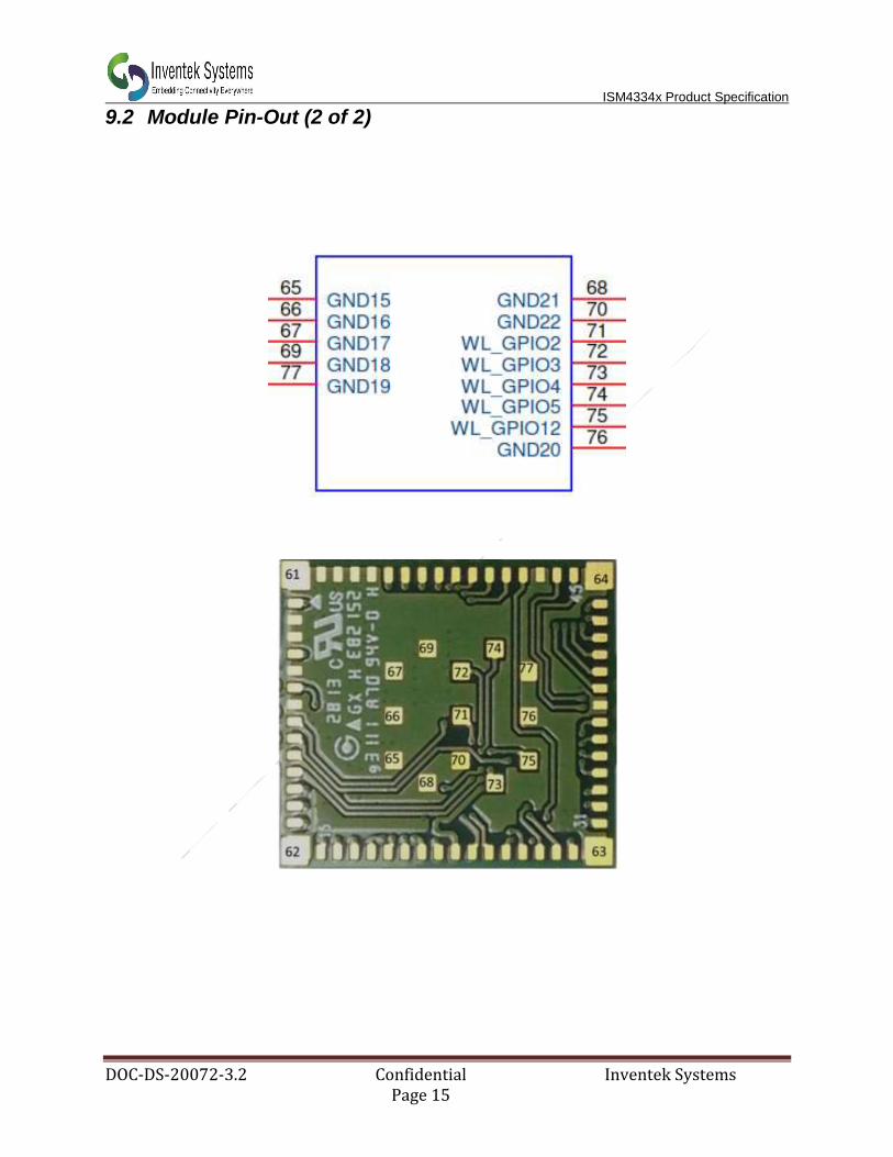
9.2 Module Pin-Out (2 of 2)

ISM4334x Product Specification
DOC-DS-20072-3.2 Confidential Inventek Systems Page 16
9.3 Recommended PCB Footprint (Bottom View)

ISM4334x Product Specification
DOC-DS-20072-3.2 Confidential Inventek Systems Page 17
9.4 Recommended PCB Footprint (Top View)

ISM4334x Product Specification
DOC-DS-20072-3.2 Confidential Inventek Systems Page 18
9.5 Detailed Pin Description
Pin No. Name TYPE Description
1 RFIN_5G RF in RF IN 5G
2 Ground G GRD
3 Ground G GRD
4 5 GHZ & 2.4 G RF in RF in
5 Ground G GRD
6 2.4 G RF in RF in RF IN 2G
7 Ground G
8 WRF_GPIO_OUT G GPIO_OUT
9 RF_SWO O Ext. RF Switch Enable -NC
10 RF_SW3 O Ext. RF Switch Enable -NC
11 RF_SW4 O Ext. RF Switch Enable -NC
12 BT_HOST_WAKE O BT_Host_Wake to Host Active High
13 32 Khz sleep clk
14 NFC_REG_PU I NFC Regulator Power Up Active High
15 BT_12S_DO BT_I2S DO
16 BT_125_CLK BT_I2S_CLK
17 BT_12S_WS BT_I2S_WS
18 BT_PCM_SYNC BT PCM Sync
19 BT_PCM_CLK BT PCM Clock
20 BT_PCM_OUT BT_PCM _Out
21 BT_PCM_IN BT_PCM In
22 BT_DEV_WAKE I BT Dev Wake up from Host Active High
23 Vio V I/O Supply Voltage ( 1.8-3.3V)
24 BT_UART_CTS_L I BT_UART_CTS_N
25 BT_UART_RTS_L O BT_UART_RTS_N
26 BT_UART_TXD I/O BT_UART_TXD
27 BT_UART_RXD I/O BT_UART_RXD
28 *NFC_VDDSWPIN_0 I NFC single wire protocol and power - UICC
29 *NFC_VDDSWP_0 O NFC single wire protocol and power
30 *NFC_RTS O NFC UART Request to Send
31 *NFC_CTS I NFC UART Clear-to-Send
32 *NFC_TX2 RF NFC antenna TX/RX Pin 2
33 *NFC_TX1 RF NFC antenna TX/RX Pin 1
34 *NFC_SDA I/O BSC data for EEPROM
35 *NFC_SCL O BSC clock for EEPROM
36 *NFC_SPI_INT I/O NFC Host Interface/Select SPI interrupt
ISM4334x Product Specification
DOC-DS-20072-3.2 Confidential Inventek Systems Page 19
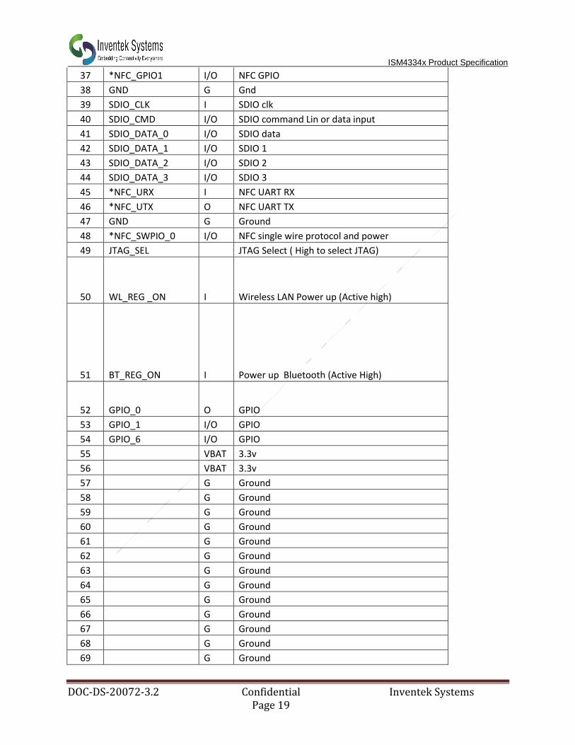
37 *NFC_GPIO1 I/O NFC GPIO
38 GND G Gnd
39 SDIO_CLK I SDIO clk
40 SDIO_CMD I/O SDIO command Lin or data input
41 SDIO_DATA_0 I/O SDIO data
42 SDIO_DATA_1 I/O SDIO 1
43 SDIO_DATA_2 I/O SDIO 2
44 SDIO_DATA_3 I/O SDIO 3
45 *NFC_URX I NFC UART RX
46 *NFC_UTX O NFC UART TX
47 GND G Ground
48 *NFC_SWPIO_0 I/O NFC single wire protocol and power
49 JTAG_SEL JTAG Select ( High to select JTAG)
50 WL_REG _ON I Wireless LAN Power up (Active high)
51 BT_REG_ON I Power up Bluetooth (Active High)
52 GPIO_0 O GPIO
53 GPIO_1 I/O GPIO
54 GPIO_6 I/O GPIO
55 VBAT 3.3v
56 VBAT 3.3v
57 G Ground
58 G Ground
59 G Ground
60 G Ground
61 G Ground
62 G Ground
63 G Ground
64 G Ground
65 G Ground
66 G Ground
67 G Ground
68 G Ground
69 G Ground

ISM4334x Product Specification
DOC-DS-20072-3.2 Confidential Inventek Systems Page 20
70 G Ground
71 WL_GPIO2 WL_GPIO2
72 WL_GPIO3 WL_GPIO3
73 WL_GPIO4 WL_GPIO4
74 WL_GPIO5 WL_GPIO5
75 WL_GPIO_12 WL_GPIO_12
76 G Ground
77 G Ground
Note: All NFC pins labelled with (*) are only available for ISM43341, and for ISM43340 these pins should
be left floating.
10 Product Compliance Considerations
RoHS: Restriction of Hazardous Substances (RoHS) directive has come into force since 1st July 2006 all electronic products sold in the EU must be free of hazardous materials, such as lead. Inventek is fully committed to being one of the first to introduce lead-free products while maintaining backwards compatibility and focusing on a continuously high level of product and manufacturing quality. EMI/EMC: The Inventek module design embeds EMI/EMC suppression features and accommodations to allow for higher operational reliability in noisier (RF) environments and easier integration compliance in host (OEM) applications.
FCC/CE: The module will be in compliance test for FCC/CE

ISM4334x Product Specification
DOC-DS-20072-3.2 Confidential Inventek Systems Page 21
11 Reflow Profile
Reference the IPC/JEDEC standard.
Peak Temperature: <250°C
Number of Times: ≤2 times

ISM4334x Product Specification
DOC-DS-20072-3.2 Confidential Inventek Systems Page 22
12 Packaging Information
12.1 MSL Level / Storage Condition

ISM4334x Product Specification
DOC-DS-20072-3.2 Confidential Inventek Systems Page 23
12.2 Device baking requirements prior to assembly
Boards must be baked prior to rework or assembly to avoid damaging moisture sensitive
components during localized reflow. The default bake cycles is 24 hours at 125C.
Maintaining proper control of moisture uptake in components is critical. Before opening the shipping bag and attempting solder reflow, you should maintain a minimal out-of-bag time and ensure the highest possible package reliability for the final product.
13 REVISION CONTROL
Document : ISM4443X Wi-Fi SIP module
External Release DOC-DS-20023
Date Author Revision Comment
1/15/2015 KMT 1.0 Preliminary 12/17/2015 KMT 1.1 Released
1/12/2016 KMT 1.2 Pin list Update 3/22/2016 KMT 3.2 Pin Description, added
Power Consumption and P/N
14 CONTACT INFORMATION
Inventek Systems 2 Republic Road Billerica Ma, 01862 Tel: 978-667-1962 [email protected] www.inventeksys.com Inventek Systems reserves the right to make changes without further notice to any products or data herein to improve reliability, function, or design. The information contained within is believed to be accurate and reliable. However Inventek Systems does not assume any liability arising out of the application or use of this information, nor the application or use of any product or circuit described herein, neither does it convey any license under its patent rights nor the rights of others.


