FN8642Rev.2.00
Jul 20, 2017
ISL9914040A DrMOS Power Module with Integrated Diode Emulation and Thermal Warning Output
DATASHEET
The ISL99140 is a high performance DrMOS power module designed for high frequency power conversion. By combining a high performance FET driver and MOSFETs in an advanced package, high density DC/DC converters can be created. Combined with an Intersil PWM controller, a complete voltage regulator solution can be created with reduced external components and minimum overall PCB real estate.
The ISL99140 features a three-state PWM input that, working together with Intersil’s multiphase PWM controllers, will provide a robust solution in the event of abnormal operating conditions. To further support robust applications, the ISL99140 features a thermal warning output that can be used to notify the power system of an impending thermal fail event.
The ISL99140 supports high efficiency operation not only at heavy loads, but also at light loads through its diode emulation capability. Diode emulation can be disabled for those applications in which variable frequency operation is not desired at light loads.
Related Literature• For a full list of related documents, visit our website
- ISL99140 product page
Features• Compliant with Intel DrMOS revision 4.0 specifications
• 40A average output current capability
• Supports 3-state 3.3V PWM input
• Supports 2-state 5V PWM input
• Thermal warning output
• Diode emulation option
• Adaptive shoot-through protection
• Integrated high-side gate-to-source resistor to prevent self turn-on due to high input bus dV/dt
• Undervoltage lockout
• Switching frequencies up to 2MHz
• Pb-free (RoHS compliant)
• 6x6 QFN package
Applications• High frequency and high efficiency VRM and VRD
• Core, graphic, and memory regulators for microprocessors
• High density VR for server, networking, and cloud computing
• POL DC/DC converters and video gaming consoles
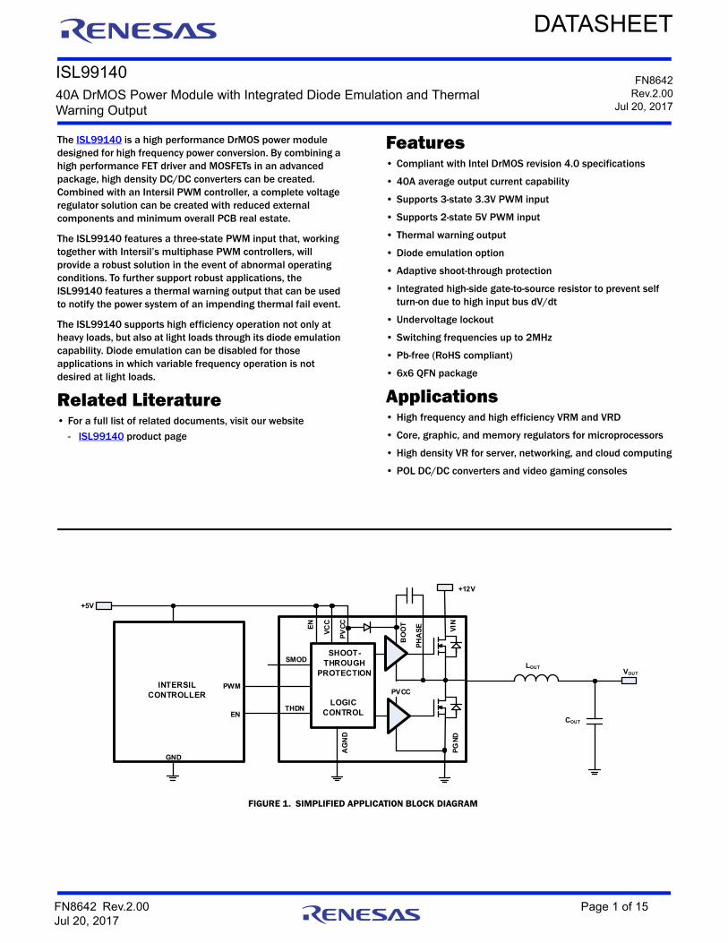
FIGURE 1. SIMPLIFIED APPLICATION BLOCK DIAGRAM
INTERSIL CONTROLLER
PWM
PHA
SE
BO
OT
+5V
ENTHDN
SHOOT- THROUGH
PROTECTION
LOGIC CONTROL
EN
VCC
PVCC
PVCC
AG
ND
PGND
VIN
+12V
GND
SMODLOUT VOUT
COUT
FN8642 Rev.2.00 Page 1 of 15Jul 20, 2017
ISL99140
Ordering InformationPART NUMBER(Notes 1, 2, 3)
PART MARKING
TEMP RANGE(°C)
TAPE AND REEL QUANTITY(UNITS)
PACKAGE(RoHS Compliant)
PKG. DWG. #
ISL99140IRZ-T 99140 IRZ -40 to +85 3k 40 Ld Exposed Pad 6x6 QFN L40.6x6A
NOTES:
1. Refer to TB347 for details on reel specifications.
2. These Intersil Pb-free plastic packaged products employ special Pb-free material sets, molding compounds/die attach materials, and 100% matte tin plate plus anneal (e3 termination finish, which is RoHS compliant and compatible with both SnPb and Pb-free soldering operations). Intersil Pb-free products are MSL classified at Pb-free peak reflow temperatures that meet or exceed the Pb-free requirements of IPC/JEDEC J STD-020.
3. For Moisture Sensitivity Level (MSL), see the product information page for ISL99140. For more information on MSL, see TB363.
TABLE 1. KEY DIFFERENCES BETWEEN FAMILY OF PARTS
PART #
CURRENTRATING
(A)PWM
(V)THERMAL
FLAGOCPFLAG IMON TMON
PACKAGEDWG. #
P2PCOMPATIBLE USED WITH
5.0V PWM POWER STAGE FAMILY
ISL99125B 25 5.0 No No No No L24.3.5x5W ISL99135B Analog Controllers: ISL633x, ISL636x, ISL637x, ISL95829, ISL9585xDigital Hybrid Controllers: ISL68201, ISL6388/98Full Digital Controller: ZL8802Phase Doublers: ISL6617, ISL6617A
ISL99135B 35 5.0 No No No No L24.3.5x5W ISL99125B
ISL99227B 60 5.0 Yes Yes Yes Yes L32.5x5V N/A
3.3V PWM POWER STAGE FAMILY
ISL99140 40 3.3 Yes No No No L40.6x6A N/A Full Digital Controllers: ISL68/69xxx, ZL8802Digital Hybrid Controllers: ISL68201, ISL6388/98 (3.3V PWM Setting)ISL99227 60 3.3 Yes Yes Yes Yes L32.5x5V N/A
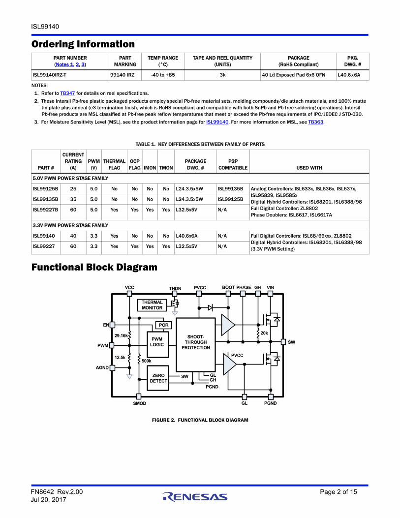
Functional Block Diagram
FIGURE 2. FUNCTIONAL BLOCK DIAGRAM
GHBOOTTHDN
SHOOT-THROUGH
PROTECTION
EN
VCC PVCC
PVCC
VIN
20kPWM
LOGIC
POR
PWM
ZERO DETECT
SW
PGNDGLSMOD
AGND
SW
PGND
PHASE
GLGH
THERMAL MONITOR
12.5k
29.16k
500k
FN8642 Rev.2.00 Page 2 of 15Jul 20, 2017

ISL99140
Pin ConfigurationISL99140
(40 LD QFN)TOP VIEW
10 9 8 7 6 5 4 3 2 1
21 22 23 24 25 26 27 28 29 30
40
39
38
37
36
35
34
33
32
31
11
12
13
14
15
16
17
18
19
20
PWM
EN
THDN
GND
GL
SW
SW
SW
SW
SW
VIN
VIN
VIN
VIN
SW
PGND
PGND
PGND
PGND
PGND
PG
ND
PG
ND
PG
ND
PG
ND
PG
ND
PG
ND
PG
ND
PG
ND
SW
SW
VIN
VIN
VIN
PH
AS
E
GH
AG
ND
BO
OT
PV
CC
VC
C
SM
OD
VINPAD2
AGNDPAD1
SWPAD3
FN8642 Rev.2.00 Page 3 of 15Jul 20, 2017
ISL99140
Pin DescriptionsPIN NUMBER PIN NAME DESCRIPTION
1 SMOD Input pin to enable or disable diode emulation with built-in pull up of 10μA. When SMOD is LOW, diode emulation is allowed. Otherwise, continuous conduction mode is forced.
2 VCC +5V logic bias supply. Place a high quality low ESR ceramic capacitor from this pin to GND.
3 PVCC +5V driver bias supply. Place a high quality low ESR ceramic capacitor from this pin to GND. VCC and PVCC often share the decoupling capacitor (~1μF/0402~0603/ X5R~X7R).
4 BOOT Floating bootstrap supply pin for the upper gate drive. Place a high quality low ESR ceramic capacitor (~0.1μF to 0.22μF) in close proximity across the BOOT and PHASE pins. A series resistor (typically 1.5 to 3.9Ω) with a bootstrap capacitor is optional, but recommended for high input voltage applications.
5, 37, PAD1 AGND, GND Return of logic bias supply VCC. Connect directly to the system ground plane.
6 GH High-side gate drive output for monitoring/testing. No circuit connection needed.
7 PHASE Return of bootstrap capacitor. Internally connected to SW node. External connection is not needed.
8, 9, 10, 11, 12, 13, 14, PAD2
VIN Input of Power Stage. Place couple high quality low ESR ceramic capacitor (couple 10μF or higher, X7R) and a high frequency decoupling capacitor (0.1μF to 1μF) in close proximity across the VIN and GND planes.
16, 17, 18, 19, 20, 21, 22, 23, 24, 25,
26, 27, 28
PGND Power Stage return. Connect directly to the system ground plane.
15, 29, 30, 31, 32, 33, 34, 35, PAD3
SW Switching junction node between low and high-side MOSFETs. Connect directly to the output inductor.
36 GL Low-side gate drive output for monitoring/testing. No circuit connection needed.
38 THDN Thermal warning flag, an output open-drain pin. High = Normal operation; Low = Shutdown.
39 EN Enable input pin with 2μA internal weak pull-down. High = Enable; Low = Disable.
40 PWM PWM input of gate driver. The PWM signal can enter three distinct states during operation. Connect this pin to the PWM output of the controller.
FN8642 Rev.2.00 Page 4 of 15Jul 20, 2017
ISL99140
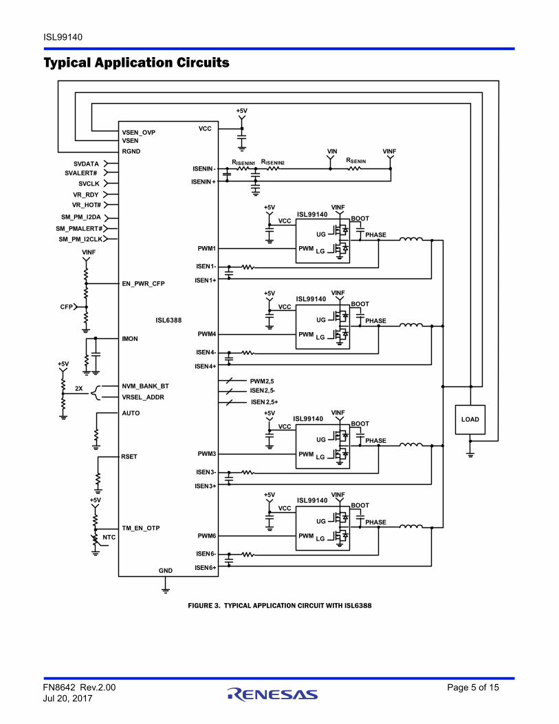
Typical Application Circuits
FIGURE 3. TYPICAL APPLICATION CIRCUIT WITH ISL6388
NTC1 NETWORK IS NOT NEEDEDIF TMS IS USED FOR VR1, GPU
VCC
IMON
SVDATA
VR_RDY
RSET
LOAD
VINF
EN_PWR_CFP
ISL6388
+5V
SM_PM_I2DA
VR_HOT#
SVCLK
SVALERT#
VINFVIN
ISENIN +
ISENIN -RISENIN1
TM_EN_OTP
+5V
NTC
RISENIN2
CFP
RSENIN
AUTO
GND
SM_PM_I2CLK
VRSEL_ADDR
NVM_BANK_BT
SM_PMALERT#
+5V
2X
ISEN1-
ISEN1+
PWM1
+5V
VCC BOOT
PHASE
VINF
PWM
ISL99140
UG
LG
ISEN4-
ISEN4+
PWM4
+5V
VCC BOOT
PHASE
VINF
PWM
ISL99140
UG
LG
ISEN3-
ISEN3+
PWM3
+5V
VCC BOOT
PHASE
VINF
PWM
ISL99140
UG
LG
ISEN6-
ISEN6+
PWM6
+5V
VCC BOOT
PHASE
VINF
PWM
ISL99140
UG
LG
ISEN2,5-
ISEN 2,5+
PWM2,5
VSENVSEN_OVP
RGND
FN8642 Rev.2.00 Page 5 of 15Jul 20, 2017
ISL99140
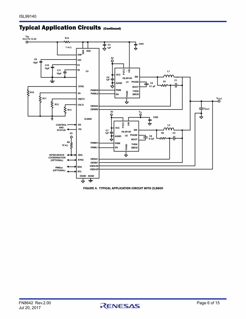
FIGURE 4. TYPICAL APPLICATION CIRCUIT WITH ZL8800
Typical Application Circuits (Continued)
VIN
VOUT
COUT
ZL8800
PWMH0
PWMH1
VIN
VDD
SDA
SCL
PG
EN
SGNDDGND
PWML0
PWML1
DDC
10.8 TO 13.2V
ISENA0
ISENB0
ISENA1
ISENB1
INTER-DEVICECOORDINATION
(OPTIONAL)
PMBus(OPTIONAL)
CONTROL AND
STATUS
U3
ISL99140V
INP
GN
D
BOOT
PV
CC
U2
VCC
AGND
SW
PWM
EN
C8C2
C31µF
0.1µF
C9
CIN1
CIN2
L2
C1R1
R2
L1
SYNC
VSEN0N
VSEN0P
10µF
10µF
10µF
C10
C11
V25
V5
V6
R11
R12
R13
SA
VSET0
UVLO
R14
1 m
IINP
IINN
R10
SYNC
R910 k
V5
ISL99140
VIN
PG
ND
BOOT
PV
CC
U1
VCC
AGND
SW
PWM
EN
C50.1 µF
THDNSMOD
THDN
SMOD
PHASE
PHASE
5V
5V
1µFC4
1µFC7
FN8642 Rev.2.00 Page 6 of 15Jul 20, 2017
ISL99140
/
Absolute Maximum Ratings Thermal InformationContinuous Current (Notes 8) . . . . . . . . . . . . . . . . . . . . . . . . . . . . . . . . . . 40AVIN . . . . . . . . . . . . . . . . . . . . . . . . . . . . . . . . . . . . . . . . . . . . . . . . -0.3V to 30VSupply Voltage (VCC) . . . . . . . . . . . . . . . . . . . . . . . . . . . . . . . . . . . -0.3V to 7VI/O Voltage (VEN, VPWM, VSMOD, VTHDN). . . . . . . . . . . -0.3V to VCC + 0.3VBOOT Voltage (VBOOT-GND) . . . . . . . . . . -0.3V to 25V (DC) or 36V (<200ns)BOOT To PHASE Voltage (VBOOT-PHASE). . . . . . . . . . . . . . . . -0.3V to 7V (DC)
-0.3V to 9V (<10ns)PHASE Voltage . . . . . . . . . . . . . . . . . . . . . . . . . . . . . . . . . (GND - 0.3V) to 30V
(GND - 10V) (<20ns Pulse Width, 10µJ)
Thermal Resistance JA (°C/W) JC (°C/W)40 Ld 6x6 QFN Package (Notes 4, 5, 7) . . 14.5 5
Maximum Junction Temperature (Plastic Package) . . . . . . . . . . . .+150°CMaximum Storage Temperature Range . . . . . . . . . . . . . .-65°C to +150°CPb-Free Reflow Profile . . . . . . . . . . . . . . . . . . . . . . . . . . . . . . . . . . see TB493
Recommended Operating ConditionsAmbient Temperature Range . . . . . . . . . . . . . . . . . . . . . . . . -40°C to +85°CMaximum Operating Junction Temperature . . . . . . . . . . . . . . . . . . +125°CSupply Voltage, VCC, PVCC . . . . . . . . . . . . . . . . . . . . . . . . . . . . . . . . 5V 5%Input Supply Voltage, VIN (Notes 9) . . . . . . . . . . . . . . . . . . . . . . . . 0V to 20V
CAUTION: Do not operate at or near the maximum ratings listed for extended periods of time. Exposure to such conditions may adversely impact productreliability and result in failures not covered by warranty.
NOTES:
4. JA is measured in free air with the component mounted on an Intersil evaluation board with “direct attach” features. Refer to TB379 for general thermal metric information.
5. For JC, the “case temp” location is the center of the exposed metal pad on the package underside.
6. Jedec Class II pulse conditions and failure criterion used.
7. These ratings vary with PCB layout and operating conditions.
8. Limited to power dissipation, thermal management solution, junction temperature, and over-temperature trip point for continuous operation; lower power dissipation and better cooling design allow higher continuous current.
9. A tightly decoupling loop across VIN and PGND with input ceramics capacitors is required. See “PCB Layout Considerations” on page 10 for details. A resistor in series (typically 1.5 to 3.9Ω) with a bootstrap capacitor is optional, but recommended for high input voltage applications to prevent exceeding the absolute maximum ratings of the device.
Electrical Specifications TA = +25°C; VIN = 12V, VVCC = VPVCC = 5V unless otherwise noted. Boldface limits apply across the recommended operating temperature range.
PARAMETER SYMBOL TEST CONDITIONSMIN
(Note 10) TYPMAX
(Note 10) UNIT
SUPPLY CURRENT
VCC Standby Supply Bias Current IVCC EN = Low, VVCC = 5V 187 µA
EN = High, VPWM = Open 467 µA
EN = High, VPWM = 0V 664 µA
PVCC Supply Bias Current IPVCC EN = High, VPWM = 300kHz, 50% duty cycle 23 mA
EN = High, VPWM = 1MHz, 50% duty cycle 51 mA
POWER-ON RESET AND ENABLE
POR Rising Threshold VPORR 3.40 3.90 V
POR Falling Threshold VPORF 2.3 2.92 V
POR Hysteresis VPORH 570 mV
EN High Threshold VENH 2.0 V
EN Low Threshold VENL 0.8 V
EN Pull-Down Current IENL 2 µA
PWM INPUT
Pull-Up Impedance 29.1 kΩ
Pull-Down Impedance 12.5 kΩ
PWM Rising Threshold VPWMH VVCC = 5V 1.70 2.05 2.35 V
PWM Falling Threshold VPWML VVCC = 5V 0.75 1.00 1.25 V
PWM Tri-State Rising Threshold VTRIH VVCC = 5V 1.10 1.32 1.50 V
FN8642 Rev.2.00 Page 7 of 15Jul 20, 2017
ISL99140
PWM Tri-State Falling Threshold VTRIL VVCC = 5V 1.60 1.75 1.95 V
PWM Tri-State Rising Hysteresis VTRRH VVCC = 5V 310 mV
PWM Tri-State Falling Hysteresis VTRFH VVCC = 5V 310 mV
SWITCHING TIME
GH Turn-On Propagation Delay tPDHU VVCC = 5V, see Figure 5 (GL Low to GH High) 15 ns
GH Turn-Off Propagation Delay tPDLU VVCC = 5V, see Figure 5 (PWM Low to GH Low) 18 ns
GL Turn-On Propagation Delay tPDHL VVCC = 5V, see Figure 5 (GH Low to GL High) 20 ns
GL Turn-Off Propagation Delay tPDLL VVCC = 5V, see Figure 5 (PWM High to GL Low) 18 ns
GH/GL Exit Tri-State Propagation Delay tPDTS VVCC = 5V, see Figure 5 (Tri-State to GH/GL High) 20 ns
Tri-State Shutdown Hold-Off Time tTSSHD VVCC = 5V, see Figure 5 75 150 225 ns
Minimum GL On-Time in DCM tLGMIN VVCC = 5V 350 ns
SMOD INPUT
SMOD High Threshold VSMODH 2.0 V
SMOD Low Threshold VSMODL 0.8 V
SMOD Pin Pull-Up Current ISMOD 10 µA
THERMAL SHUTDOWN (THDN)
Pull-Down Impedance 1mA 60 Ω
Output Low 1mA 70 mV
Thermal Shutdown Flag Set (Note 11) 150 °C
Thermal Shutdown Flag Clear (Note 11) 135 °C
Hysteresis (Note 11) 15 °C
NOTES:
10. Parameters with MIN and/or MAX limits are 100% tested at +25°C, unless otherwise specified. Temperature limits established by characterization and are not production tested.
11. Limits established by characterization and are not production tested.
Electrical Specifications TA = +25°C; VIN = 12V, VVCC = VPVCC = 5V unless otherwise noted. Boldface limits apply across the recommended operating temperature range. (Continued)
PARAMETER SYMBOL TEST CONDITIONSMIN
(Note 10) TYPMAX
(Note 10) UNIT
FN8642 Rev.2.00 Page 8 of 15Jul 20, 2017

ISL99140
Operation The ISL99140 is an optimized driver and power stage solution for high density synchronous DC/DC power conversion. The ISL99140 includes a high performance driver, integrated Schottky bootstrap diode, and MOSFET pair optimized for high switching frequency buck voltage regulators. The ISL99140 includes a driver with advanced power management features that allow direct control of the Lower MOSFET, diode emulation, and thermal protection.
Power-On Reset (POR) and ENDuring initial start-up, the VCC voltage rise is monitored. When the rising VCC voltage exceeds 3.40V (typically), normal operation of the driver is enabled. If VCC drops below the falling threshold of 2.92V (typically), operation of the driver is disabled.
If the EN pin is pulled low, the driver will immediately force both MOSFETS to their off states. This action does not depend on the state of the PWM input.
Shoot-Through ProtectionBefore VCC exceeding its POR level, the undervoltage protection function is activated and both GH and GL are held active low (off). When the VCC voltage surpasses the Rising Threshold (see “Electrical Specifications” on page 7) the PWM, SMOD, and DE signals are used to control both high-side and low-side MOSFETs.
The rising edge on PWM initiates the turn-off of the lower MOSFET. Adaptive shoot-through circuitry monitors the GL voltage and determines a safe time for the upper MOSFET to turn on. This prevents the MOSFET’s from conducting simultaneously.
The falling PWM transition causes the upper FET to turn off and the lower FET to turn-on. Adaptive shoot-through circuitry monitors the GH to SW voltage to determine a safe time for low-side MOSFET turn-on. This prevents the MOSFETs from conducting simultaneously.
If the driver has no bias voltage applied and is unable to actively hold the MOSFETs off, an integrated 20kΩ resistor from the upper MOSFET gate-to-source will aid in keeping the device in its off state. This can be especially critical in applications where the input voltage rises before the ISL99140 VCC /PVCC supplies.
Tri-State PWM InputThe ISL99140 supports a tri-level input on the PWM pin. If the pin is pulled into and remains in the tri-state window for a set holdoff time, the driver will force both MOSFETs to their off states. When the PWM signal moves outside the shutdown window, the driver immediately resumes driving the MOSFETs according to the PWM commands.
This feature is used by Intersil PWM controllers as a method of forcing both MOSFETs off. If the PWM input is left floating, the pin will be pulled into the tri-state window internally and force both MOSFETs to a safe off state. The ISL99140’s tri-state levels are compatible with 3.3V PWM logic.
FIGURE 5. TIMING DIAGRAM
PWM
UGATE
LGATE
tFL
tPDHU
tPDLL
tRL
tTSSHD
tPDTS
tPDTS
tFUtRU
tPDLU
tPDHL
tTSSHD
TABLE 2. GATE DRIVE TRUTH TABLE
ENABLE SMOD PWM GL GH
L X X L L
H L L H (Note 12) L
H L H L H
H H L H L
H H H L H
NOTE:12. The GL stays high until the inductor current drops to zero.
FN8642 Rev.2.00 Page 9 of 15Jul 20, 2017

ISL99140
Although PWM input can sustain as high as VCC, the ISL99140 is not compatible with a controller (such as ISL637x family) that actively drives its mid level in tri-state higher than 1.7V. However, the ISL99140 can be configured to be compatible with ZL8800 by connecting PWMH to PWM and PWML to EN, as shown in Figure 4 on page 6. In this example, the tri-state operation is controlled by PWML output of ZL8800 through ISL99140’s EN input. For detailed design information, consult the ZL8800 datasheet.
Diode EmulationDiode emulation allows for higher converter efficiency under light load situations. With diode emulation active (SMOD pulled low), the ISL99140 will detect the zero current crossing of the output inductor and turn off the low-side gate after the minimum LGATE ON time of 350ns expires. This ensures that Discontinuous Conduction Mode (DCM) is achieved to minimize losses. Diode emulation is asynchronous to the PWM signal. Therefore, the ISL99140 will respond to the SMOD input immediately after it changes state.
Bootstrap FunctionThe ISL99140 features an internal bootstrap Schottky diode. A high quality ceramic capacitor should be placed in close proximity across the BOOT and PHASE pins. The bootstrap capacitor can range between 0.1µF~0.22µF/0402~0603/X5R~X7R for normal buck switching applications. A resistor (typically 1.5Ω to 3.9Ω) in series with a bootstrap capacitor is optional, but recommended for high input voltage application to prevent exceeding the absolute maximum ratings of the device.
Thermal Shutdown Warning (THDN)The THDN pin is an open-drain output and is pulled low when the internal junction temperature exceeds +150°C. The ISL99140 does not stop operation when the flag is set. This signal is often fed back to the controller to issue a system thermal shutdown. When the junction temperature drops below +135°C, the device will clear the THDN signal.
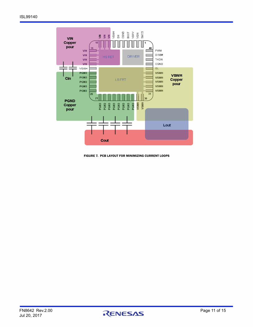
PCB Layout ConsiderationsProper PCB layout will reduce noise coupling to other circuits, improve thermal performance, and maximize the efficiency. The following is meant to lead to an optimized layout:
• Place a 0.1µF and multiple 10µF or greater ceramic capacitors directly at device between VIN and PGND as indicated in Figure 7. This is the most critical decoupling and reduces parasitic inductance in the power switching loop. This will reduce overall electrical stress on the device as well as reduce coupling to other circuits. Best practice is to place the decoupling capacitors on the same PCB side as the device.
• Connect PGND to the system GND plane with a large via array as close to the PGND pins as design rules allow. This improves thermal and electrical performance.
• Place PVCC, VCC, and BOOT-PHASE decoupling capacitors at the IC pins with the shortest loop as shown in Figure 7.
• Note that the SW plane connecting the ISL99140 and inductor must carry full load current and will create resistive loss if not sized properly. However, it is also a very noisy node that should not be oversized or routed close to any sensitive signals. Best practice is to place the inductor as close to the device as possible and thus minimize the required area for the SW connection. If the user must choose a long route of either the VOUT side of the inductor or the SW side, choose the quiet VOUT side. Best practice is to locate the ISL99140 as close to the final load as possible and thus avoid noisy or lossy routes to the load.
FIGURE 6. BOOT RESISTOR OPTION
ISL99140
VIN
PG
ND
PHASE
PV
CC
U1
VCC
AGND
SW
PWM
EN
THDN
SMOD
BOOT
5V
1µF
CBT
RBT
RBT is optional, but recommendedfor high VIN
TABLE 3. AVAILABLE EVALUATION BOARDS
EVALUATION BOARDS DESCRIPTIONSMBus/
PMBus/I2C
ISL6388EVAL1Z 6-Phase Core VR with ISL99140, 6x6 DrMOS, and the ISL6388, EAPP Digital Controller; Socket R3 Yes
ISL6398EVAL1Z 3-Phase POL VR with ISL99140, 6x6 DrMOS, and the ISL6388, EAPP Digital Controller; On-Board Transient Load Yes
FN8642 Rev.2.00 Page 10 of 15Jul 20, 2017
ISL99140
FIGURE 7. PCB LAYOUT FOR MINIMIZING CURRENT LOOPS
FN8642 Rev.2.00 Page 11 of 15Jul 20, 2017
ISL99140
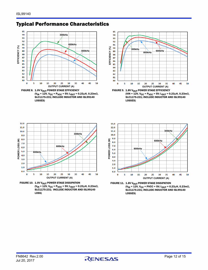
Typical Performance Characteristics
FIGURE 8. 1.0V VOUT POWER STAGE EFFICIENCY (VIN = 12V, VCC = PVCC = 5V; LOUT = 0.23µH, 0.23mΩ, SLC1175-231; INCLUDE INDUCTOR AND ISL99140 LOSSES)
FIGURE 9. 1.8V VOUT POWER STAGE EFFICIENCY (VIN = 12V, VCC = PVCC = 5V; LOUT = 0.23µH, 0.23mΩ, SLC1175-231; INCLUDE INDUCTOR AND ISL99140 LOSSES)
FIGURE 10. 1.0V VOUT POWER STAGE DISSIPATION (VIN = 12V, VCC = PVCC = 5V; LOUT = 0.23µH, 0.23mΩ,SLC1175-231; INCLUDE INDUCTOR AND ISL99140 LOSS)
FIGURE 11. 1.8V VOUT POWER STAGE DISSIPATION (VIN = 12V, VCC = PVCC = 5V; LOUT = 0.23µH, 0.23mΩ, SLC1175-231; INCLUDE INDUCTOR AND ISL99140 LOSSES)
300kHz
600kHz
800kHz
OUTPUT CURRENT (A)
EF
FIC
IEN
CY
(%
)
800kHz 300kHz
600kHz
OUTPUT CURRENT (A)
EF
FIC
IEN
CY
(%
)
800kHz
300kHz
600kHz
PO
WE
R L
OS
S (
W)
OUTPUT CURRENT (A)
PO
WE
R L
OS
S (
W)
OUTPUT CURRENT (A)
800kHz
300kHz
600kHz
FN8642 Rev.2.00 Page 12 of 15Jul 20, 2017
ISL99140
Intersil products are manufactured, assembled and tested utilizing ISO9001 quality systems as notedin the quality certifications found at www.intersil.com/en/support/qualandreliability.html
Intersil products are sold by description only. Intersil may modify the circuit design and/or specifications of products at any time without notice, provided that such modification does not, in Intersil's sole judgment, affect the form, fit or function of the product. Accordingly, the reader is cautioned to verify that datasheets are current before placing orders. Information furnished by Intersil is believed to be accurate and reliable. However, no responsibility is assumed by Intersil or its subsidiaries for its use; nor for any infringements of patents or other rights of third parties which may result from its use. No license is granted by implication or otherwise under any patent or patent rights of Intersil or its subsidiaries.
For information regarding Intersil Corporation and its products, see www.intersil.com
For additional products, see www.intersil.com/en/products.html
© Copyright Intersil Americas LLC 2014-2017. All Rights Reserved.All trademarks and registered trademarks are the property of their respective owners.
About IntersilIntersil Corporation is a leading provider of innovative power management and precision analog solutions. The company's products address some of the largest markets within the industrial and infrastructure, mobile computing, and high-end consumer markets.
For the most updated datasheet, application notes, related documentation, and related parts, see the respective product information page found at www.intersil.com.
For a listing of definitions and abbreviations of common terms used in our documents, visit www.intersil.com/glossary.
You can report errors or suggestions for improving this datasheet by visiting www.intersil.com/ask.
Reliability reports are also available from our website at www.intersil.com/support.
Revision History The revision history provided is for informational purposes only and is believed to be accurate, but not warranted. Please visit our website to make sure that you have the latest revision.
DATE REVISION CHANGE
Jul 20, 2017 FN8642.2 Updated Related Literature section.Added Table 1.Updated the BOOT and VIN pin descriptions.Added 40A continuous current under absolute maximum ratings.Updated Theta JA value from “50” to “14.5”.Updated Note 4.Added Notes 7, 8, and 9.Opened up the recommended VIN range from “4.5V to 18V” to “0 to 20V”. In “Power-On Reset (POR) and EN” on page 9, changed “3.5V” to “3.4V” and “2.95V” to “2.92V” to match page 7 in the “Electrical Specifications” table. Updated Note 12, corrected typo LG to GL.Updated “Bootstrap Function” on page 10.Added “a 0.1µF and” on first bullet and “the with shortest loop” on the third bullet under PCB Layout Considerations.
Jan 7, 2016 FN8642.1 Updated the Ordering Information table on page 2 by adding the tape and reel quantity.Under “Absolute Maximum Ratings” on page 7, added the following:“Phase Voltage............................(GND - 0.3V) to 30V
(GND-10V) (<20ns Pulse Width, 10µJ)
May 5, 2014 FN8642.0 Initial release
FN8642 Rev.2.00 Page 13 of 15Jul 20, 2017

ISL99140
Package Outline DrawingL40.6x6A40 LEAD THIN QUAD FLAT NO-LEAD PLASTIC PACKAGE
Rev 0, 3/14
11
21
1
31 20
30
40
D/2
D
2
INDEX AREA(D/2 x E/2)
B
A
E/2
e
A3
TOP VIEW
2x
2xaaa C
10
SEATINGPLANE
C
40 x b
A
SIDE VIEW
4
Cbbb M A B3
ddd C A1
A3ccc C
11
21
1
31 20
30
10
40
PIN #1 IDA
D1
D2
D1
L1
L1
ee/2
L5
L5L
C0.30 x 45°
BOTTOM VIEW
L2E1 E1
E2
L6
L
L3
L4
Coplanarity applies to the terminals and all other
measured between 0.20mm and 0.35mm from the Dimension b applies to metallized terminal and is
The location of the terminal #1 identifier and
4.
3.
2.
Dimensions are in millimeters.1.
NOTES:
E
aaa
C
terminal numbering convention conforms to
terminal tip. If the terminal has the optional radiuson the other end of the terminal, the dimension b
bottom surface metallization.
DIMENSIONS IN MILLIMETERS
SYMBOLS MIN TYP MAX
0.73L3
0.260.210.15L2
0.250.200.15L1
0.80
0.05
0.75
0.02
2.00
0.70
0.00
A
A1
E
D2
D1
6.00 BSC
bbb
aaa
L
A3 0.20 REF
0.350.250.20b
0.500.400.30
0.50 BSC
D 6.00 BSC
E1
ccc
ddd
0.15
0.10
0.10
0.08
1.40 1.601.50
e
1.90 2.10
4.30 4.40 4.50
E2 2.17 2.372.27
0.830.63
0.54L4 0.640.44
0.37L6 0.470.27
0.40L5 0.500.30
should not be measured in that radius area.
JEDEC publication 95 SPP-002.
FN8642 Rev.2.00 Page 14 of 15Jul 20, 2017

ISL99140
0.30 x 45°
0.73
1.50
0.52
0.21
2.23
2.27
2.20
4.40
2.002.00
0.20
0.50 REF
0.37
0.55
0.54
RECOMMENDED LAND PATTERN
0.25
0.25
0.40
0.20
2.87 2.87
2.87
2.87
0.75
Dimensions are in millimeters.1.
NOTE:
FN8642 Rev.2.00 Page 15 of 15Jul 20, 2017


