
ECE 3040 - Dr. Alan DoolittleGeorgia Tech
Lecture 25
MOSFET Basics (Understanding with Math)
Reading: Pierret 17.1-17.2 and Jaeger 4.1-4.10 and Notes

ECE 3040 - Dr. Alan DoolittleGeorgia Tech
MOS Transistor I-V Derivation
With our expression relating the Gate voltage to the surface potential and the fact that S=2F we can determine the value of the threshold voltage
areaunit per ecapacitanc oxide theis
where,
devices) channel-p(for 222
devices) channel-n(for 22
2
ox
oxox
FS
D
ox
SFT
FS
A
ox
SFT
xC
qNC
V
qNC
V
Where we have made use of the use of the expression,
oSS K

ECE 3040 - Dr. Alan DoolittleGeorgia Tech
MOS Transistor I-V Derivation
Coordinate Definitions for our “NMOS” Transistor
x=depth into the semiconductor from the oxide interface.
y=length along the channel from the source contact
z=width of the channel
xc(y) = channel depth (varies along the length of the channel).
n(x,y)= electron concentration at point (x,y)
n(x,y)=the mobility of the carriers at point (x,y)
Device width is Z
Channel Length is L
Assume a “Long Channel” device (for now do not worry about the channel length modulation effect)
ECE 3040 - Dr. Alan DoolittleGeorgia Tech
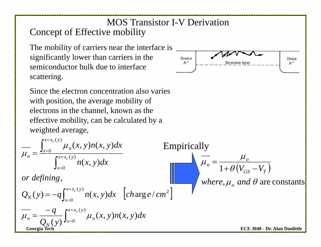
MOS Transistor I-V DerivationConcept of Effective mobilityThe mobility of carriers near the interface is significantly lower than carriers in the semiconductor bulk due to interface scattering.
Since the electron concentration also varies with position, the average mobility of electrons in the channel, known as the effective mobility, can be calculated by a weighted average,
)(
0
2)(
0
)(
0
)(
0
),(),()(
/arg),()(
,
),(
),(),(
yxx
x nN
n
yxx
xN
yxx
x
yxx
x nn
c
c
c
c
dxyxnyxyQ
q
cmechdxyxnqyQ
definingor
dxyxn
dxyxnyx
Empirically
constants are ,
1
andwhereVV
o
TGS
on
ECE 3040 - Dr. Alan DoolittleGeorgia Tech
MOS Transistor I-V Derivation
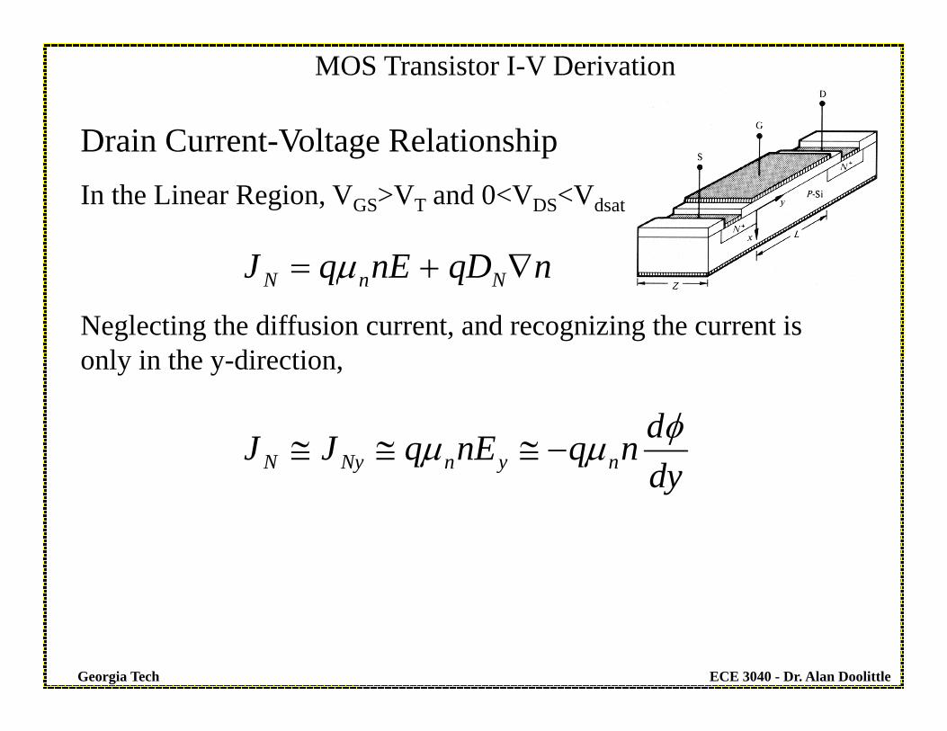
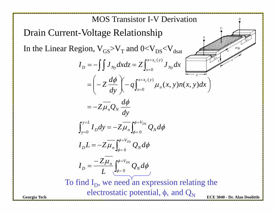
Drain Current-Voltage RelationshipIn the Linear Region, VGS>VT and 0<VDS<Vdsat
dydnqnEqJJ
nqDnEqJ
nynNyN
NnN
Neglecting the diffusion current, and recognizing the current is only in the y-direction,
ECE 3040 - Dr. Alan DoolittleGeorgia Tech
MOS Transistor I-V Derivation
Drain Current-Voltage RelationshipIn the Linear Region, VGS>VT and 0<VDS<Vdsat
DS
DS
DS
c
c
V
Nn
D
V
NnD
V
Nn
Ly
y D
Nn
yxx
x n
yxx
x NyNyD
dQLZI
dQZLI
dQZdyI
dydQZ
dxyxnyxqdydZ
dxJZdxdzJI
0
0
00
)(
0
)(
0
),(),(
To find ID, we need an expression relating the electrostatic potential, and QN

ECE 3040 - Dr. Alan DoolittleGeorgia Tech
MOS Transistor I-V Derivation“Capacitor-Like” Model for QNAssumptions:•Neglect all but the mobile inversion charge (valid for deep inversion)•For the MOSFET, the charge in the semiconductor is a linear function of position along the semiconductor side of the plate. Thus, varies from 0 to VDS
MOS Capacitor MOS Transistor
TGS VVfor TGSoxN VVCQ
TGS VVfor TGSoxN VVCQ
Source Drain
,dVdQCSince ox
Neglect the depletion region chargeNote: Assuming a linear variation of potential along the channel leads to an underestimation of current but is a good estimate for hand calculations.
Only voltages above threshold create inversion charge
ECE 3040 - Dr. Alan DoolittleGeorgia Tech
MOS Transistor I-V Derivation
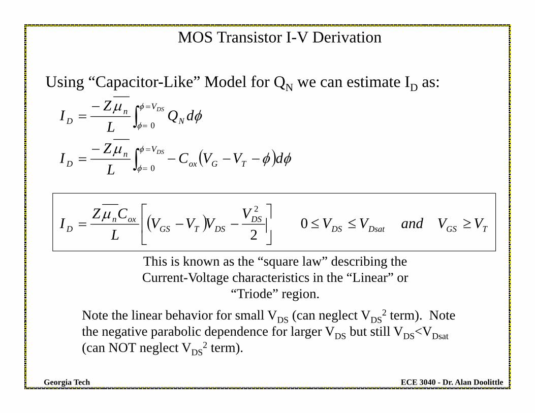
Using “Capacitor-Like” Model for QN we can estimate ID as:
TGSDsatDSDS
DSTGSoxn
D
V
TGoxn
D
V
Nn
D
VVandVVV
VVVLCZ
I
dVVCLZ
I
dQLZ
I
DS
DS
02
2
0
0
This is known as the “square law” describing the Current-Voltage characteristics in the “Linear” or
“Triode” region.Note the linear behavior for small VDS (can neglect VDS
2 term). Note the negative parabolic dependence for larger VDS but still VDS<VDsat(can NOT neglect VDS
2 term).
ECE 3040 - Dr. Alan DoolittleGeorgia Tech
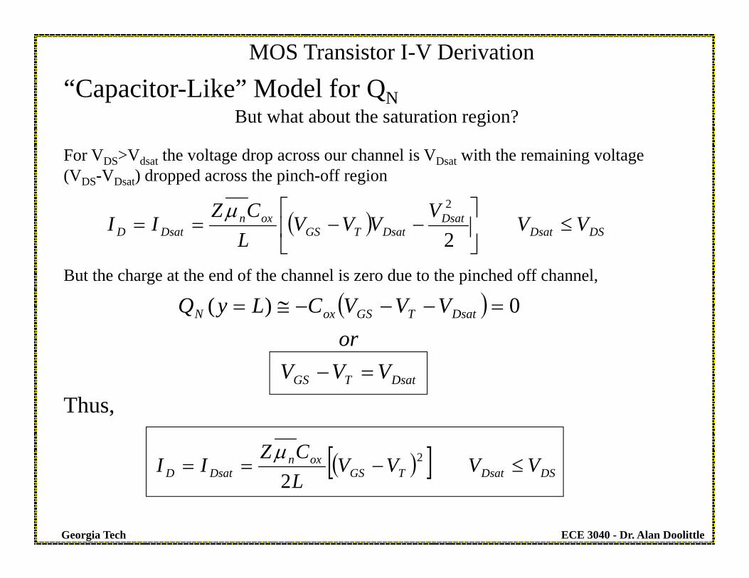
MOS Transistor I-V Derivation
“Capacitor-Like” Model for QN
For VDS>Vdsat the voltage drop across our channel is VDsat with the remaining voltage (VDS-VDsat) dropped across the pinch-off region
DSDsatDsat
DsatTGSoxn
DsatD VVV
VVVLCZ
II
2
2
But the charge at the end of the channel is zero due to the pinched off channel,
DsatTGS
DsatTGSoxN
VVVor
VVVCLyQ
0)(
Thus,
DSDsatTGSoxn
DsatD VVVVLCZ
II 2
2
But what about the saturation region?

ECE 3040 - Dr. Alan DoolittleGeorgia Tech
MOS Transistor I-V Derivation
TGSDsat VVV
DSDsatTGSoxn
DsatD VVVVLCZ
II 2
2
TGSDsatDS
DSDSTGS
oxnD
VVandVV
VVVV
LCZ
I
02
2
Summary of MOSFET IV Relationship
ECE 3040 - Dr. Alan DoolittleGeorgia Tech
MOS Transistor Applications
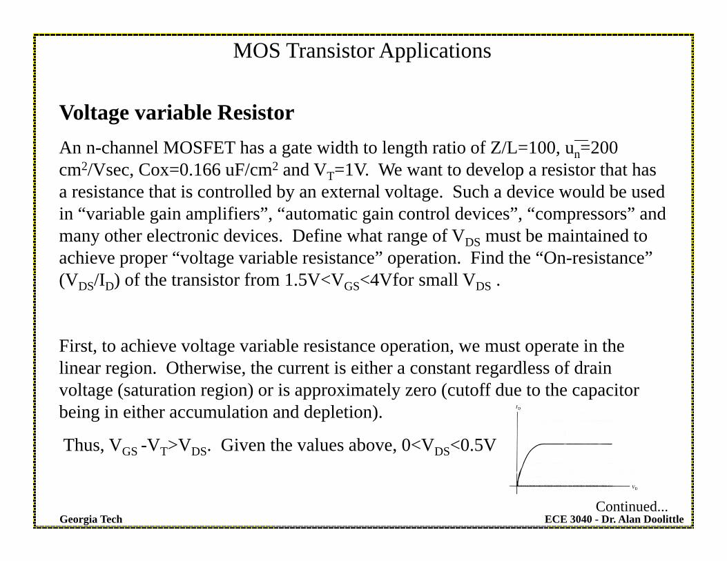
Voltage variable ResistorAn n-channel MOSFET has a gate width to length ratio of Z/L=100, un=200 cm2/Vsec, Cox=0.166 uF/cm2 and VT=1V. We want to develop a resistor that has a resistance that is controlled by an external voltage. Such a device would be used in “variable gain amplifiers”, “automatic gain control devices”, “compressors” and many other electronic devices. Define what range of VDS must be maintained to achieve proper “voltage variable resistance” operation. Find the “On-resistance” (VDS/ID) of the transistor from 1.5V<VGS<4Vfor small VDS .
First, to achieve voltage variable resistance operation, we must operate in the linear region. Otherwise, the current is either a constant regardless of drain voltage (saturation region) or is approximately zero (cutoff due to the capacitor being in either accumulation and depletion).
Thus, VGS -VT>VDS. Given the values above, 0<VDS<0.5V
Continued...

ECE 3040 - Dr. Alan DoolittleGeorgia Tech
MOS Transistor Applications
Voltage variable ResistorUsing the linear region ID equation:
600100,
1/6166.020001.0
V smallfor 2
2
DS
2
DS
GSDS
TGSoxnDSTGS
oxn
DS
D
DSDS
DSTGSoxnDS
DSTGSoxn
D
RThus
VcmFeR
VVCZ
L
VVVLCZ
VI
VR
VVVLCZV
VVVLCZ
I
ECE 3040 - Dr. Alan DoolittleGeorgia Tech
MOS Transistor Applications
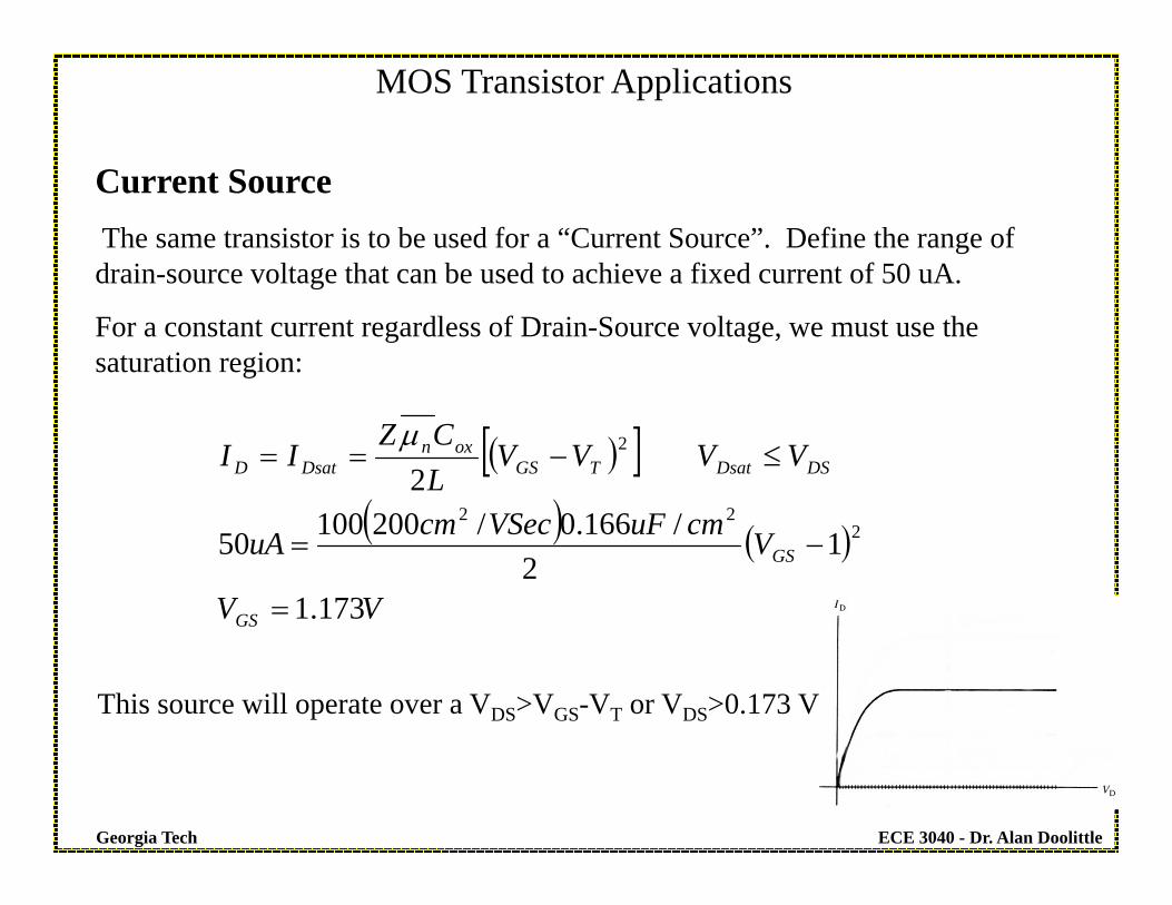
Current SourceThe same transistor is to be used for a “Current Source”. Define the range of drain-source voltage that can be used to achieve a fixed current of 50 uA.
For a constant current regardless of Drain-Source voltage, we must use the saturation region:
VV
VcmuFVSeccmuA
VVVVLCZ
II
GS
GS
DSDsatTGSoxn
DsatD
173.1
12
/166.0/20010050
22
22
2
This source will operate over a VDS>VGS-VT or VDS>0.173 V
ECE 3040 - Dr. Alan DoolittleGeorgia Tech
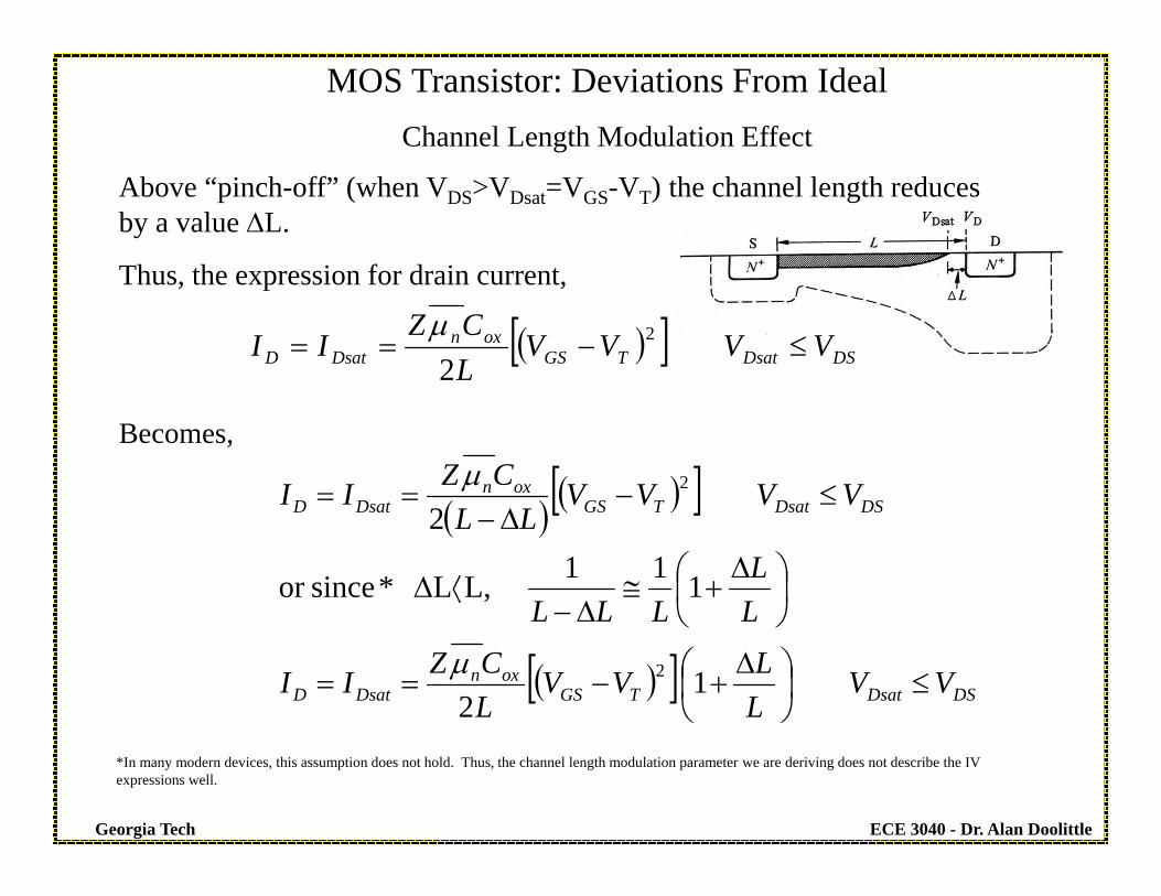
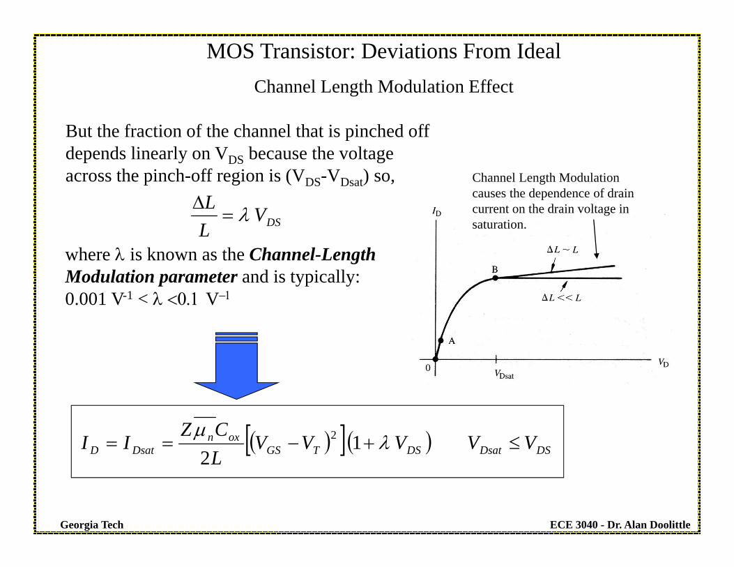
MOS Transistor: Deviations From IdealChannel Length Modulation Effect
Above “pinch-off” (when VDS>VDsat=VGS-VT) the channel length reduces by a value L.
Thus, the expression for drain current,
Becomes,
DSDsatTGSoxn
DsatD VVVVLCZ
II 2
2
DSDsatTGSoxn
DsatD
DSDsatTGSoxn
DsatD
VVLLVV
LCZII
LL
LLL
VVVVLL
CZII
12
111 L,L *sinceor
2
2
2
*In many modern devices, this assumption does not hold. Thus, the channel length modulation parameter we are deriving does not describe the IV expressions well.
ECE 3040 - Dr. Alan DoolittleGeorgia Tech
MOS Transistor: Deviations From IdealChannel Length Modulation Effect
DSVLL
But the fraction of the channel that is pinched off depends linearly on VDS because the voltage across the pinch-off region is (VDS-VDsat) so,
DSDsatDSTGSoxn
DsatD VVVVVLCZ
II
12
2
where is known as the Channel-Length Modulation parameter and is typically: 0.001 V-1 < V
Channel Length Modulation causes the dependence of drain current on the drain voltage in saturation.

ECE 3040 - Dr. Alan DoolittleGeorgia Tech
MOS Transistor: Deviations From IdealBody Effect (Substrate Biasing)
Until now, we have only considered the case where the substrate (Body) has been grounded….
…but the substrate (Body) is often intentionally biased such that the Source-Body and Drain-Body junctions are reversed biased.
The body bias, VBS, is known as the backgate bias and can be used to modify the threshold voltage.
Note that now our channel potential has an offset equal to VBS, ….

ECE 3040 - Dr. Alan DoolittleGeorgia Tech
devices) channel-p(for 22
2
devices) channel-n (for222
FS
D
ox
SFT
FS
A
ox
SFT
qNC
V
qNC
V
MOS Transistor: Deviations From IdealBody Effect (Substrate Biasing)
Thus, our threshold potential with the body grounded,
The Gate- Body Threshold becomes,
devices) channel-n(for 222
devices) channel-p(for 222
BSFS
A
ox
SBSFGB
BSFS
D
ox
SBSFGB
VqNC
VV
VqNC
VV
Threshold
Threshold
But we would like to have this in terms of VGS instead of VGB.
Since, VGS =VGB+VBS
devices) channel-p(for 22
2
devices) channel-n(for 222
BSFS
D
ox
SFGS
BSFS
A
ox
SFGS
VqN
CV
VqNC
V
Threshold
Threshold
Surface Potential S
VT=
ECE 3040 - Dr. Alan DoolittleGeorgia Tech
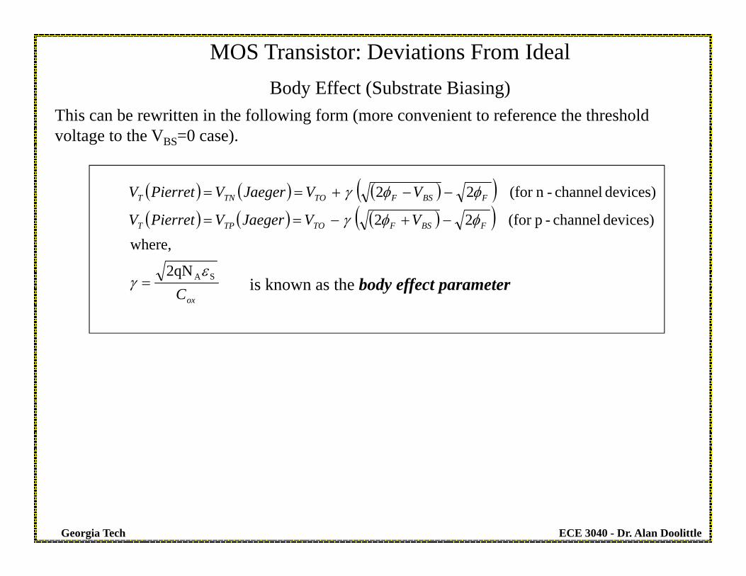
MOS Transistor: Deviations From IdealBody Effect (Substrate Biasing)
ox
FBSFTOTPT
FBSFTOTNT
C
VVJaegerVPierretV
VVJaegerVPierretV
SA2qN
where,devices) channel-p(for 22
devices) channel-n(for 22
This can be rewritten in the following form (more convenient to reference the threshold voltage to the VBS=0 case).
is known as the body effect parameter

ECE 3040 - Dr. Alan DoolittleGeorgia Tech
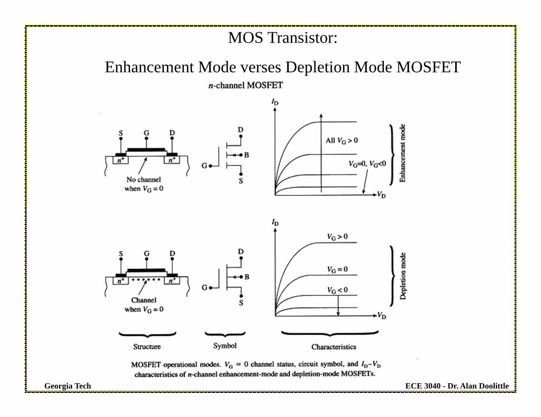
MOS Transistor:
Enhancement Mode verses Depletion Mode MOSFET
We have been studying the “enhancement mode” MOSFET (Metal-Oxide-Semiconductor Field Effect Transistor). It is called “enhancement” because conduction occurs only after the channel conductance is “improved” or “enhanced”. In this case,
VTN>0 and VTP<0
Transistors can be fabricated such that:
These transistors have conduction for VGS=0 due to a channel already existing without the need to “invert the near surface region”. To modulate currents, a field must applied to the gate that depletes the channel. Thus, transistors of this nature are called “Depletion mode MOSFETs”.
0V and 0V TPTN
ECE 3040 - Dr. Alan DoolittleGeorgia Tech
MOS Transistor:
Enhancement Mode verses Depletion Mode MOSFET
ECE 3040 - Dr. Alan DoolittleGeorgia Tech
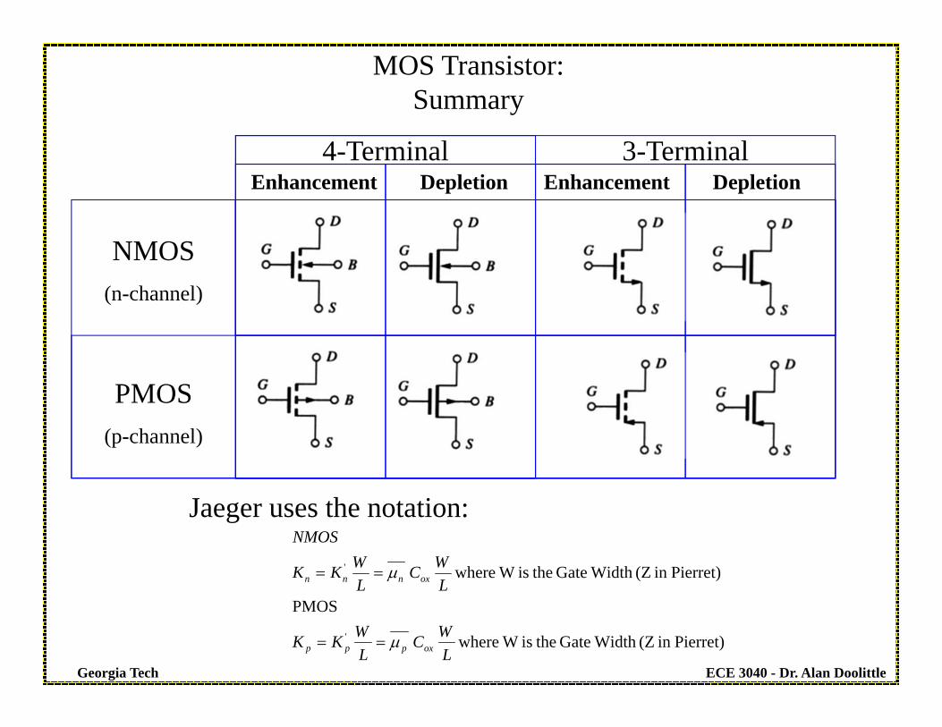
MOS Transistor: Summary
Jaeger uses the notation:
Pierret)in (Z Width Gate theisW where
PMOS
Pierret)in (Z Width Gate theisW where
'
'
LWC
LWKK
LWC
LWKK
NMOS
oxppp
oxnnn
4-Terminal 3-Terminal
NMOS(n-channel)
PMOS(p-channel)
Enhancement EnhancementDepletion Depletion

ECE 3040 - Dr. Alan DoolittleGeorgia Tech
MOS Transistor: Summary
NMOS PMOSRegardless of Mode
Cutoff
Linear
Saturation
Threshold Voltage
VT for Enhancement Mode
VT for Depletion Mode
Pierret)in Z W:(Note ' LWC
LWKK oxnnn Pierret)in ZW :(Note '
LWC
LWKK oxppp
TNGSDS VVforI 0 TPGSDS VVforI 0
0
12
2
TNGSDSTNGS
DSTNGSoxn
DS
VVVandVV
VVVLCZ
I
0
12
2
TPGSDSTPGS
DSTPGSoxn
DS
VVVandVV
VVVLCZ
I
02
2
DSTNGSTNGS
DSDSTNGS
oxnDS
VVVandVV
VVVV
LCZ
I
0
2
2
DSTPGSTPGS
DSDSTPGS
oxnD
VVVandVV
VVVV
LCZ
I
0TNV
0TNV
0TPV
0TPV
FBSFTOTP VVV 22 FSBFTOTN VVV 22

ECE 3040 - Dr. Alan DoolittleGeorgia Tech
MOS Transistor: Bias Circuitry-Enhancement Mode NMOS
Due to zero DC current flow in the gate, the bias analysis of a MOSFET is significantly easier than a BJT.
A B
C •Form Thevenin circuits looking out the gate, drain, and source

ECE 3040 - Dr. Alan DoolittleGeorgia Tech
DSDS
GSthG
VRIVVRIV
310
3
•But IG=0 so VGS=3V
•Assume Saturation operation (selected for easy math because IDS does not depend on VDS since no was given – =0):
DS
DS
TNGSDSTNGSn
DS
VCheck
Axi
VvvforVvK
i
501321025
02
26
2
VVVVVVkuAV
TNGSDS
DS
25)100(5010
•Assumption of Saturation operation was correct! If it were not correct simply make another assumption (I.e. linear region) and resolve.
MOS Transistor: Bias Circuitry-Enhancement Mode NMOS
IDS
IG

ECE 3040 - Dr. Alan DoolittleGeorgia Tech
MOS Transistor: Bias Circuitry-Depletion Mode NMOS
•Bias circuit of a depletion mode device is much simpler due to the fact that the device conducts drain current for VGS=0V
•What value of R1 results in 100 uA drain current?•Again Assuming saturation:
2200
0
3
VuAK
V
VV
n
TO
VVVVVVV
VkuAVRIVVCheck
KuAI
VR
VVuA
uAVKI
VV
VvvforVvK
i
TNGSDS
DSDSDS
DS
DS
GS
n
DSTNGS
TNGSDSTNGSn
DS
1)3(2820100110
20100
21
2/200
100232
02
2
2
IDS
•Assumption of Saturation operation was correct! If it were not correct simply make another assumption (I.e. linear region) and resolve.

ECE 3040 - Dr. Alan DoolittleGeorgia Tech
PMOS Transistor: Bias Circuitry-Enhancement Mode PMOS
225
0
1
VuAK
V
VV
p
TO
0)1(66.208.60
08.6
4.34166.22
62566.271.2021.7051.0
12
625000,394610
2
6005.1||1615.1
5.110
02
12
2
2
2
2
22
TPGSDS
DS
DSDDDSSDDD
D
GSGSGS
GSGS
GSTPGSp
SEQDD
EQGGGSSSDD
EQEQ
TPGSDSTPGS
TPGSp
DSTPGSoxn
SD
VVVVCheck
VVRIVRIV
AEI
VorVVV
VVE
VVVK
RVV
VRIVRIV
KMMRVMM
MVV
VVVandVV
VVK
VVVLCZ
II

ECE 3040 - Dr. Alan DoolittleGeorgia Tech
MOS Transistor: Bias Circuitry-Possible Combinations
SourcethDrainthSourcethDSDSDrainth
DSDSTNGSnDSDSTNGS
nDS
SourcethSourcethDSGSBaseth
VRRIVVoptionallyand
VVVVKIorVVVKI
VRIVV
____
22
___
)3,
21
2)2
)1
•Always: Solve 1) for VGS and plug into 2). •In certain cases, VDS will need to be eliminated by using 3) solved for VDS and plugged into 2).
•Case A: Saturated, and =0 and no source resistor –only 1 and 2 required. Results in 1st order polynomial.•Case B: Saturated, and >0 and no source resistor – all 3 equations needed. Results in 1st order polynomial.•Case C: Saturated, and =0 and a source resistor – all 3 equations needed. Results in 2nd order polynomial.•Case D: Saturated, and >0 and a source resistor – all 3 equations needed. Results in 3rd order polynomial.•Case E: Linear/Triode, with or without a source resistor – all 3 equations needed. Results in 2nd order polynomial.
Assume either saturated or linear/triode.

ECE 3040 - Dr. Alan DoolittleGeorgia Tech
Useful Formulas for DC Bias SolutionsIf a 3rd order polynomial results, try factoring it into a linear and quadratic term 1st. If this is not easy for your case, a longer but sure fire way is listed below.


