Physics 9826b
February 11, 13, 2013 1
1
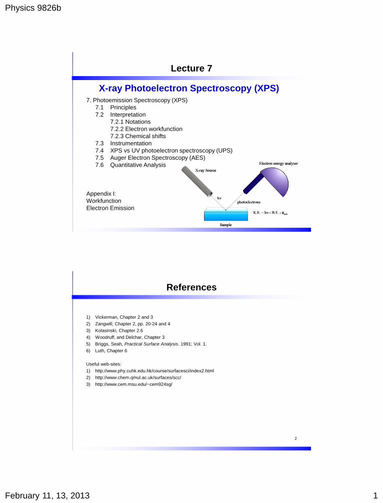
Lecture 7
X-ray Photoelectron Spectroscopy (XPS) 7. Photoemission Spectroscopy (XPS)
7.1 Principles
7.2 Interpretation
7.2.1 Notations
7.2.2 Electron workfunction
7.2.3 Chemical shifts
7.3 Instrumentation
7.4 XPS vs UV photoelectron spectroscopy (UPS)
7.5 Auger Electron Spectroscopy (AES)
7.6 Quantitative Analysis
Appendix I:
Workfunction
Electron Emission
References
2
1) Vickerman, Chapter 2 and 3
2) Zangwill; Chapter 2, pp. 20-24 and 4
3) Kolasinski, Chapter 2.6
4) Woodruff, and Delchar, Chapter 3
5) Briggs, Seah, Practical Surface Analysis. 1991; Vol. 1.
6) Luth, Chapter 6
Useful web-sites:
1) http://www.phy.cuhk.edu.hk/course/surfacesci/index2.html
2) http://www.chem.qmul.ac.uk/surfaces/scc/
3) http://www.cem.msu.edu/~cem924sg/

Physics 9826b
February 11, 13, 2013 2
3
Electron Spectroscopy for Chemical Analysis
Spectroscopy Particles involved Incident
Energy
What you learn
XPS
X-ray Photoelectron
X-ray in
e out
1-4 keV Chemical state,
composition
UPS
UV Photoelectron
UV photon
e out
5-500 eV Valence band
AES
Auger Electron
e in, e out;
radiationless process,
filling of core hole
1-5 keV Composition, depth
profiling
IPS
Inverse Photoelectron
e in
photon out
8-20eV Unoccupied states
EELS
Electron Energy Loss
e in
e out
1-5 eV Vibrations
4
7.1 Photoemission Spectroscopy: Principles
Electrons absorb X-ray photon and are ejected from atom
Energy balance:
Photon energy – Kinetic Energy = Binding Energy
hn - KE = BE
• Spectrum – Kinetic energy
distribution of photoemitted e’s
• Different orbitals give different peaks
in spectrum
• Peak intensities depend on
photoionization cross section (largest
for C 1s)
• Extra peak: Auger emission
Physics 9826b
February 11, 13, 2013 3
10/3/2010 Lecture 5 5
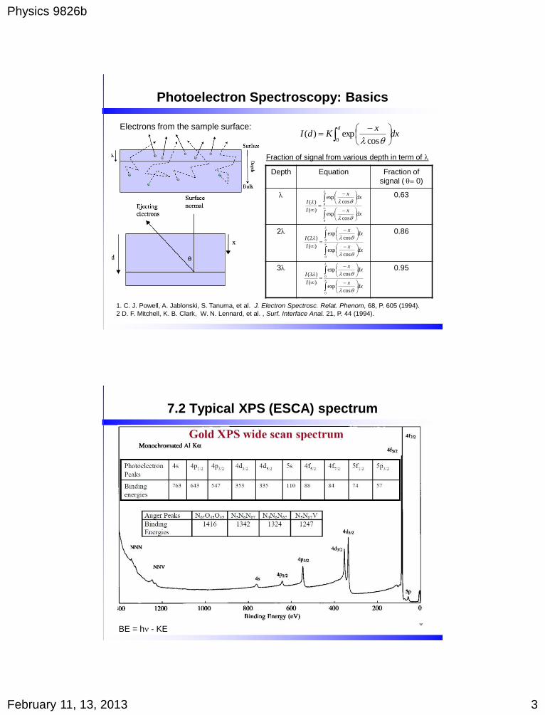
Photoelectron Spectroscopy: Basics
Electrons from the sample surface: dx
xKdI
d
-
0 cosexp)(
1. C. J. Powell, A. Jablonski, S. Tanuma, et al. J. Electron Spectrosc. Relat. Phenom, 68, P. 605 (1994).
2 D. F. Mitchell, K. B. Clark, W. N. Lennard, et al. , Surf. Interface Anal. 21, P. 44 (1994).
Fraction of signal from various depth in term of
Depth Equation Fraction of
signal ( 0)
0.63
2
0.86
3
0.95
dxx
dxx
I
I
-
-
0
0
cosexp
cosexp
)(
)(
dxx
dxx
I
I
-
-
0
0
cosexp
cosexp
)(
)2(
dxx
dxx
I
I
-
-
0
0
cosexp
cosexp
)(
)3(
6
7.2 Typical XPS (ESCA) spectrum
BE = hn - KE
Physics 9826b
February 11, 13, 2013 4
7
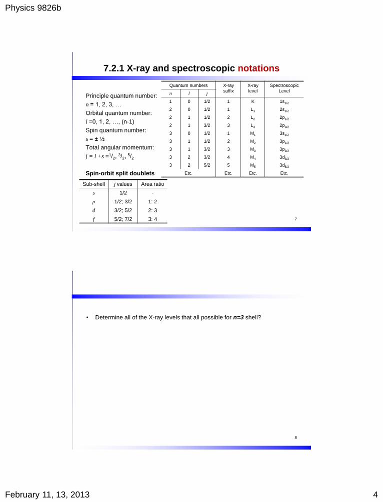
7.2.1 X-ray and spectroscopic notations
Principle quantum number:
n = 1, 2, 3, …
Orbital quantum number:
l =0, 1, 2, …, (n-1)
Spin quantum number:
s = ± ½
Total angular momentum:
j = l +s =1/2, 3/2,
5/2
Spin-orbit split doublets
Quantum numbers X-ray
suffix
X-ray
level
Spectroscopic
Level n l j
1 0 1/2 1 K 1s1/2
2 0 1/2 1 L1 2s1/2
2 1 1/2 2 L2 2p1/2
2 1 3/2 3 L3 2p3/2
3 0 1/2 1 M1 3s1/2
3 1 1/2 2 M2 3p1/2
3 1 3/2 3 M3 3p3/2
3 2 3/2 4 M4 3d3/2
3 2 5/2 5 M5 3d5/2
Etc. Etc. Etc. Etc.
Sub-shell j values Area ratio
s 1/2 -
p 1/2; 3/2 1: 2
d 3/2; 5/2 2: 3
f 5/2; 7/2 3: 4
• Determine all of the X-ray levels that all possible for n=3 shell?
8

Physics 9826b
February 11, 13, 2013 5
10/3/2010 Lecture 5 9
Binding energy reference in XPS
Energy level diagram for an electrically conductive sample grounded to the
spectrometer
• common to calibrate the
spectrometer by the
photoelectron peaks of Au
4f 7/2, Ag 3d5/2 or Cu 2p3/2
• the Fermi levels of the
sample and the
spectrometer are aligned;
• KE of the photoelectrons
is measured from the EF of
the spectrometer.
10
• The “true work function” of a uniform surface of an electronic
conductor is defined as the difference between the electrochemical
potential of the electrons just inside the conductor, and the electrostatic
potential energy of an electron in the vacuum just outside
• is work required to bring an electron isothermally from infinity to solid
• Note: is function of internal AND surface/external (e.g., shifting charges,
dipoles) conditions;
• We can define quantity m which is function of internal state of the solid
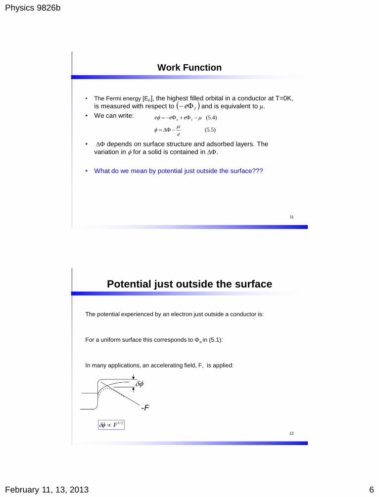
7.2.2 Work Function: Uniform Surfaces
e
m oe-
m
m
Energ
y
distance
oe-
me
m
Ie-
Ie mm Average electrostatic potential inside Chemical potential of electrons:
Physics 9826b
February 11, 13, 2013 6
11
Work Function
• The Fermi energy [EF], the highest filled orbital in a conductor at T=0K,
is measured with respect to and is equivalent to m.
• We can write:
• D depends on surface structure and adsorbed layers. The
variation in for a solid is contained in D.
• What do we mean by potential just outside the surface???
Ie-
(5.5)
(5.4)
e
eee Io
m
m
-D
--
12
Potential just outside the surface
The potential experienced by an electron just outside a conductor is:
For a uniform surface this corresponds to o in (5.1):
In many applications, an accelerating field, F, is applied:
2/1F
Physics 9826b
February 11, 13, 2013 7
13
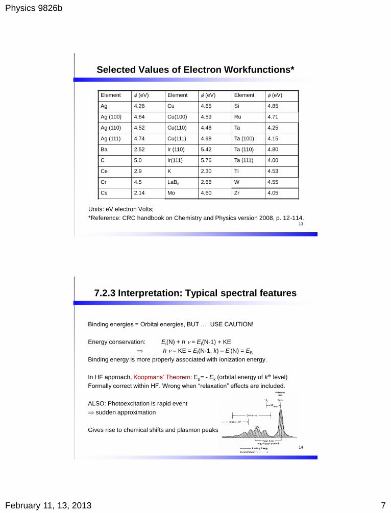
Selected Values of Electron Workfunctions*
Units: eV electron Volts;
*Reference: CRC handbook on Chemistry and Physics version 2008, p. 12-114.
Element (eV) Element (eV) Element (eV)
Ag 4.26 Cu 4.65 Si 4.85
Ag (100) 4.64 Cu(100) 4.59 Ru 4.71
Ag (110) 4.52 Cu(110) 4.48 Ta 4.25
Ag (111) 4.74 Cu(111) 4.98 Ta (100) 4.15
Ba 2.52 Ir (110) 5.42 Ta (110) 4.80
C 5.0 Ir(111) 5.76 Ta (111) 4.00
Ce 2.9 K 2.30 Ti 4.53
Cr 4.5 LaB6 2.66 W 4.55
Cs 2.14 Mo 4.60 Zr 4.05
14
7.2.3 Interpretation: Typical spectral features
Binding energies = Orbital energies, BUT … USE CAUTION!
Energy conservation: Ei(N) + h n = Ef(N-1) + KE
h n – KE = Ef(N-1, k) – Ei(N) = EB
Binding energy is more properly associated with ionization energy.
In HF approach, Koopmans’ Theorem: EB= - Ek (orbital energy of kth level)
Formally correct within HF. Wrong when “relaxation” effects are included.
ALSO: Photoexcitation is rapid event
sudden approximation
Gives rise to chemical shifts and plasmon peaks

Physics 9826b
February 11, 13, 2013 8
15
Qualitative results
A: Identify element
B: Chemical shifts of core levels:
Consider core levels of the same element in different chemical states:
DEB = EB(2) – EB(1) = EK(2) – EK(1)
Often correct to associate ∆EB with change in local electrostatic potential due to change in
electron density associated with chemical bonding (“initial state effects”).
Chemical Shifts
Core binding energies are determined by:
electrostatic interaction between it and the nucleus, and reduced by
• …
• …
16
Physics 9826b
February 11, 13, 2013 9
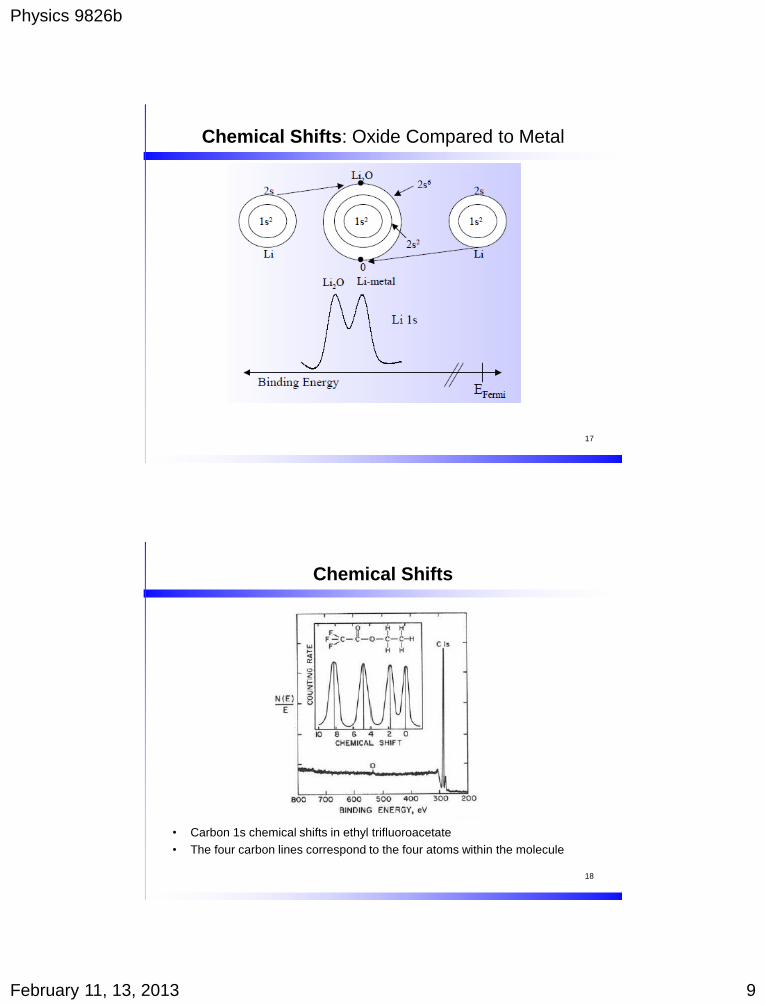
Chemical Shifts: Oxide Compared to Metal
17
18
Chemical Shifts
• Carbon 1s chemical shifts in ethyl trifluoroacetate
• The four carbon lines correspond to the four atoms within the molecule
Physics 9826b
February 11, 13, 2013 10
19
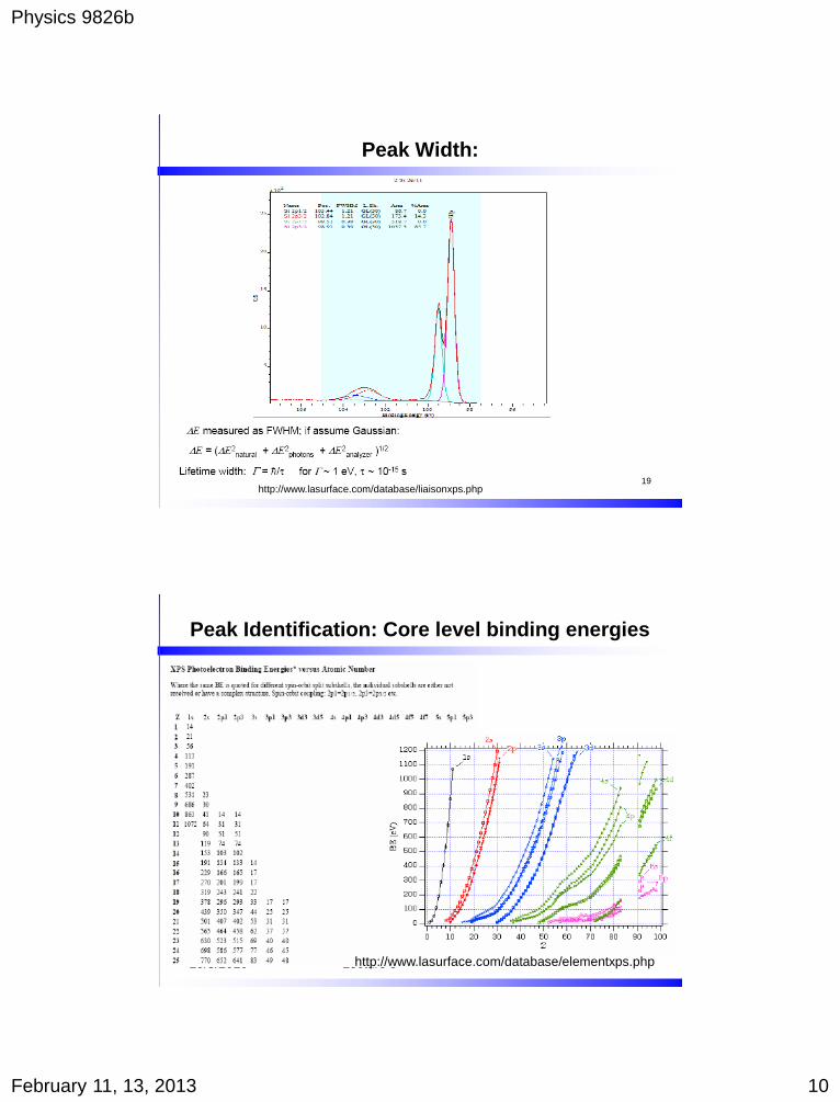
Peak Width:
http://www.lasurface.com/database/liaisonxps.php
10/3/2010 Lecture 5 20
Peak Identification: Core level binding energies
http://www.lasurface.com/database/elementxps.php

Physics 9826b
February 11, 13, 2013 11
How to measure peak intensities?
21
• Accuracy better than 15%
• Use of standards measured
on same instrument or full
expression above accuracy
better than 5%
• In both cases, reproducibility
(precision) better than 2%
22
Quantification of XPS
Primary assumption for quantitative analysis: ionization
probability (photoemission cross section) of a core level is
nearly independent of valence state for a given element
intensity number of atoms in detection volume
ddxdydzdz
zyxNEyxTyxJLEDIyx x
AAAAAA
-
0
2
0 ,
0cos
exp),,(),,,,(),()()()(
where:
A = photoionization cross section
D(EA) = detection efficiency of spectrometer at EA
LA() = angular asymmetry of photoemission intensity
= angle between incident X-rays and detector
J0(x,y) = flux of primary photons into surface at point (x,y)
T = analyzer transmission
= azimuthal angle
NA(x,y,z) = density of A atoms at (x,y,z)
M = electron attenuation length of e’s with energy EA in matrix M
= detection angle (between sample normal and spectrometer)
Physics 9826b
February 11, 13, 2013 12
23
Quantitative analysis
For small entrance aperture (fixed , ) and uniform illuminated sample:
Angles i and i are fixed by the sample geometry and
G(EA)=product of area analyzed
and analyzer transmission function
D(EA)=const for spectrometers
Operating at fixed pass energy
A: well described by Scofield
Calculation of cross-section
)(cos)()()()( 0 AiAMAiAAAA EGENJLEDI
yx
AA dxdyEyxTEG,
),,()(
24
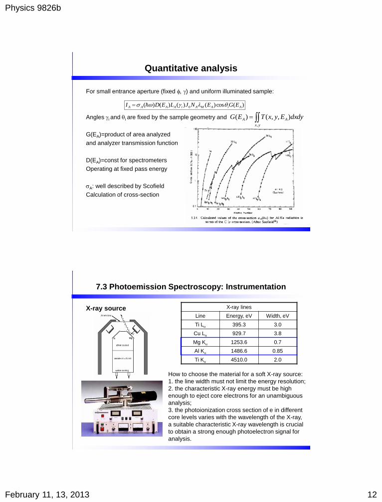
7.3 Photoemission Spectroscopy: Instrumentation
X-ray source
X-ray lines
Line Energy, eV Width, eV
Ti La 395.3 3.0
Cu La 929.7 3.8
Mg Ka 1253.6 0.7
Al Ka 1486.6 0.85
Ti Ka 4510.0 2.0
How to choose the material for a soft X-ray source:
1. the line width must not limit the energy resolution;
2. the characteristic X-ray energy must be high
enough to eject core electrons for an unambiguous
analysis;
3. the photoionization cross section of e in different
core levels varies with the wavelength of the X-ray,
a suitable characteristic X-ray wavelength is crucial
to obtain a strong enough photoelectron signal for
analysis.
Physics 9826b
February 11, 13, 2013 13
25
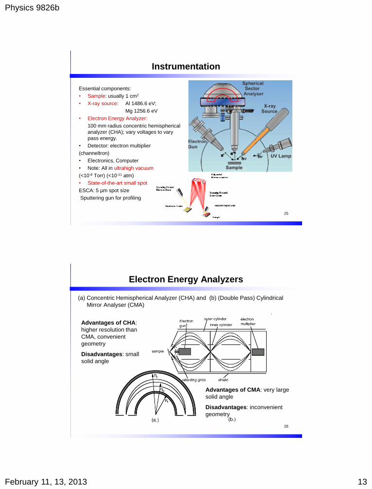
Instrumentation
Essential components:
• Sample: usually 1 cm2
• X-ray source: Al 1486.6 eV;
Mg 1256.6 eV
• Electron Energy Analyzer:
100 mm radius concentric hemispherical
analyzer (CHA); vary voltages to vary
pass energy.
• Detector: electron multiplier
(channeltron)
• Electronics, Computer
• Note: All in ultrahigh vacuum
(<10-8 Torr) (<10-11 atm)
• State-of-the-art small spot
ESCA: 5 µm spot size
Sputtering gun for profiling
26
Electron Energy Analyzers
(a) Concentric Hemispherical Analyzer (CHA) and (b) (Double Pass) Cylindrical
Mirror Analyser (CMA)
Advantages of CHA:
higher resolution than
CMA, convenient
geometry
Disadvantages: small
solid angle
Advantages of CMA: very large
solid angle
Disadvantages: inconvenient
geometry

Physics 9826b
February 11, 13, 2013 14
27
Surface Science Western- XPS
http://www.uwo.ca/ssw/services/xps.html
http://xpsfitting.blogspot.com/
http://www.casaxps.com/
http://www.lasurface.com/database/elementxps.php
Kratos Axis Ultra (left)
Axis Nova (right)
Contact:
Mark Biesinger
10/3/2010 Lecture 5 28
7.4 Comparison XPS and UPS
XPS: photon energy hn=200-4000 eV to probe
core-levels (to identify elements and their
chemical states).
UPS: photon energy hn=10-45 eV to probe filled
electron states in valence band or adsorbed
molecules on metal.
Angle resolved UPS can be used to map band
structure ( to be discussed later)
UPS source of irradiation: He discharging lamp
(two strong lines at 21.2 eV and 42.4 eV,
termed He I and He II) with narrow line width
and high flux
Synchrotron radiation source
continuously variable phootn energy, can be
made vaery narrow, very intense, now widely
available, require a monochromator
Introduction to Photoemission Spectroscopy in solids, by F. Boscherini
http://amscampus.cib.unibo.it/archive/00002071/01/photoemission_spectroscopy.pdf

Physics 9826b
February 11, 13, 2013 15
29
Studies with UV Photoemission
• The electronic structure of solids -detailed angle resolved
studies permit the complete band structure to be mapped out in
k-space
• The adsorption of molecules on solids-by comparison of the
molecular orbitals of the adsorbed species with those of both
the isolated molecule and with calculations.
• The distinction between UPS and XPS is becoming less and
less well defined due to the important role now played by
synchrotron radiation.
Lecture 5 30
7.5 Auger Electron Spectroscopy (AES)
• Steps in Auger deexcitation
• Note: The energy of the Auger electrons
do not depend on the energy of the
projectile electron in (a)!
Physics 9826b
February 11, 13, 2013 16
31
Auger spectrum of Cu(001) and CuP
Sections of Auger electron spectra, showing Cu (M2,3VV)
and P (L2,3VV) transitions, for a low temperature PH3
overlayer phase at 140K and (b) for a P c (68)
structure obtained by annealing the surface of (a) to
Tx > 450K. Both spectra have been normalized to
give the same Cu (60 eV) feature peak height.
30 60 90 120 150
(b)
(a)
140K
Tx = 323K
P (122eV)
P (118eV)
P (113eV)
P (122eV)
P (119eV)
Cu
(105eV)
Cu
(60eV)
x
x
dN
(E)/
dE
Energy [eV]
PH3/Cu(001)
0 200 400 600 800 1000
x 3O
CCu(KLL)
Cu(001)
Tx = 323K
Ep = 2keV
Cu(LMM)
dN
/dE
Auger Electron Energy [eV]
(b)
Use dN/dE (derivative mode)
Why?
• Are Auger peaks recorded at 60eV, 350eV and 1500eV equally surface
sensitive?
32

Physics 9826b
February 11, 13, 2013 17
33
Applications of AES
• A means of monitoring surface cleanliness of samples
• High sensitivity (typically ca. 1% monolayer) for all elements except H and
He.
• Quantitative compositional analysis of the surface region of specimens, by
comparison with standard samples of known composition.
• The basic technique has also been adapted for use in :
–Auger Depth Profiling : providing quantitative compositional information as
a function of depth below the surface (through sputtering)
–Scanning Auger Microscopy (SAM) : providing spatially-resolved
compositional information on heterogeneous samples (by scanning the
electron beam over the sample)
10/3/2010 Lecture 5 34
7.6 Quantitative analysis
Physics 9826b
February 11, 13, 2013 18
Depth Profiling
35
36
Quantitative Analysis
• Estimate chemical concentration,
chemical state, spatial distribution of
surface species
• Simplest approximation is that
sample is in single phase

Physics 9826b
February 11, 13, 2013 19
Appendix I
• Workfunction of polycrystalline materials
• Electron emission
References:
1) Zangwill, p.57-63
2) Woodruff & Delchar, pp. 410-422, 461-484
3) Luth, pp.336, 437-443, 464-471
4) A. Modinos, “Field, Thermionic and Secondary Electron Spectroscopy”,
Plenum, NY 1984.
37
38
Work Function: Polycrystalline Surfaces
Consider polycrystalline surface with “patches” of different
workfunction, and different value of surface potential
At small distance ro above ith patch electrostatic potential is oi
At distances large w/r/t/ patch dimension:
So mean work function is given by:
- at low applied field, electron emission controlled by:
- at high field (applied field >> patch field)
electron emission related to individual patches:
On real surfaces, patch dimension < 100Å, if ∆~ 2 eV then patch
field F ~ 2V/(10-6 cm ) ~ 2 x 10⁶ Volts/cm. work required to
bring an electron from infinity to solid
i, oi j, … k l
m m o p
patch i of area fractional , thff i
i
oiio
(5.10) i
iiefe
e
ie
Physics 9826b
February 11, 13, 2013 20
39
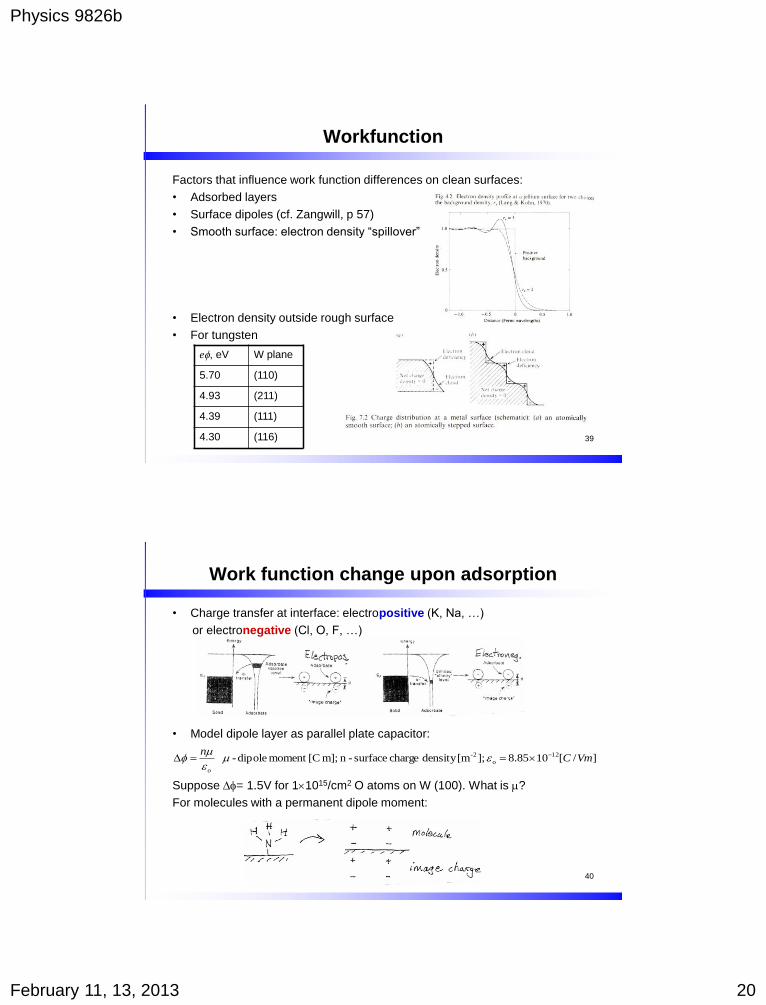
Workfunction
Factors that influence work function differences on clean surfaces:
• Adsorbed layers
• Surface dipoles (cf. Zangwill, p 57)
• Smooth surface: electron density “spillover”
• Electron density outside rough surface
• For tungsten
e, eV W plane
5.70 (110)
4.93 (211)
4.39 (111)
4.30 (116)
Lecture 7 40
Work function change upon adsorption
• Charge transfer at interface: electropositive (K, Na, …)
or electronegative (Cl, O, F, …)
• Model dipole layer as parallel plate capacitor:
Suppose D= 1.5V for 11015/cm2 O atoms on W (100). What is m?
For molecules with a permanent dipole moment:
]/[1085.8 ];[mdensity charge surface -n m]; [Cmoment dipole- 12
o
2- VmCn
o
-D m
m
Physics 9826b
February 11, 13, 2013 21
41
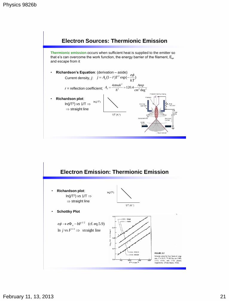
Electron Sources: Thermionic Emission
• Richardson’s Equation: (derivation – aside)
Current density, j:
r = reflection coefficient;
• Richardson plot:
ln(j/T2) vs 1/T
straight line
)exp()1( 2
kT
eTrAj o
--
223
2
deg4.120
4
cm
Amp
h
mekAo
Thermionic emission occurs when sufficient heat is supplied to the emitter so
that e’s can overcome the work function, the energy barrier of the filament, Ew,
and escape from it
42
Electron Emission: Thermionic Emission
• Richardson plot:
ln(j/T2) vs 1/T
straight line
• Schottky Plot
linestraight vsln
eq.5.9) (cf.
2/1
2/1
-
Fj
bFee o

Physics 9826b
February 11, 13, 2013 22
43
Field Electron Emission
• Electron tunneling through low, thin barrier
– Field emission, when F>3107 V/cm ~ 0.3 V/Å
• General relation for electron emission in high field:
• P is given by WKB approximation
• If approximate barrier by triangle:
• Fowler – Nordheim eqn, including potential barrier:
ZZZ dEEvFEPej )(),(0
--
l
Z dzEVm
constP0
2/12/13/2
)(2
exp
FF
2/32/1
2
1~
2
1~
-
F
mconstP
2/32/13/22exp
2/12/32/372
26 where;
)(1083.6exp)(1054.1
Fey
F
yfyt
Fj
- -
44
How do we get high fields: Field Emission Microscope!
Get high field by placing sharp tip at
center of spherical tube.
Mag: R/r ~ 5cm/10-5cm ~ 500,000
F = cV; c ~ 5/r F ~ 5 x 10⁷ V/cm
For V = 2,500 Volts.
W single crystal wire as tip.
Typical pattern on phosphor screen
Physics 9826b
February 11, 13, 2013 23
Lecture 7 45
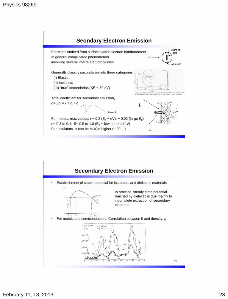
Seondary Electron Emission
Electrons emitted from surfaces after electron bombardment
In general complicated phenomenon
involving several interrelated processes
Generally classify secondaries into three categories:
- (I) Elastic ;
- (II) Inelastic;
- (III) “true” secondaries (KE < 50 eV)
Total coefficient for secondary emission,
σ= j2/ji = r + η + δ
For metals, max values: r ~ 0.2 (Ep ~ eV); ~ 0.02 (large Ep)
η~ 0.3 to 0.4; δ~ 0.5 to 1.8 (Ep ~ few hundred eV)
For insulators, can be MUCH higher (~ 20!!!!)
j2
j1
Lecture 7 46
Secondary Electron Emission
• Establishment of stable potential for insulators and dielectric materials
• For metals and semiconductors: Correlation between δ and density, ρ
In practice, steady state potential
reached by dielectic is due mainly to
incomplete extraction of secondary
electrons


