LOW-TEMPERATURE SCANNING MAGNETIC PROBE MICROSCOPY
OF EXOTIC SUPERCONDUCTORS
A DISSERTATION
SUBMITTED TO THE DEPARTMENT OF APPLIED PHYSICS
AND THE COMMITTEE ON GRADUATE STUDIES
OF STANFORD UNIVERSITY
IN PARTIAL FULFILLMENT OF THE REQUIREMENTS
FOR THE DEGREE OF
DOCTOR OF PHILOSOPHY
Per G. Bjornsson
September 2005

c© Copyright by Per G. Bjornsson 2005
All Rights Reserved
ii
I certify that I have read this dissertation and that, in my opinion, it is fully
adequate in scope and quality as a dissertation for the degree of Doctor of
Philosophy.
Kathryn A. Moler Principal Adviser
I certify that I have read this dissertation and that, in my opinion, it is fully
adequate in scope and quality as a dissertation for the degree of Doctor of
Philosophy.
Ian R. Fisher
I certify that I have read this dissertation and that, in my opinion, it is fully
adequate in scope and quality as a dissertation for the degree of Doctor of
Philosophy.
Steven A. Kivelson
Approved for the University Committee on Graduate Studies.
iii

iv
Abstract
Scanning magnetic probe microscopy is one of the many scanning probe microscopy
(SPM) techniques that have been developed in the last two decades. The basic idea
of the technique is conceptually simple: a micro- or nano-scale magnetic sensor is
rastered over a sample and measures the magnetic field locally, giving an image of
the magnetic fields at the surface. This thesis details the construction of a scanning
magnetic microscope which utilizes SQUID (Superconducting QUantum Interference
Device) or Hall probe sensors in a dilution refrigerator, extending the temperature
range for this measurement technique down to the millikelvin range; the development
of the probes used in the microscope; and the measurements for which it has been used.
The primary experiment which I report is searching for signs of time reversal sym-
metry breaking in the unconventional superconductor strontium ruthenate (Sr2RuO4).
There is strong published evidence that this material is a spin-triplet superconduc-
tor. In addition, there is experimental evidence from µSR (muon spin resonance) and
small-angle neutron scattering experiments that the wavefunction is a two-component
Ginzburg-Landau wavefunction which exhibits time reversal symmetry breaking (TRSB)
properties.
A direct consequence of TRSB is that there should be spontaneously generated
magnetic fields locally at sample edges. I have searched for this signature of TRSB in
single-crystal samples of Sr2RuO4, including samples that have been patterned with an
array of dimples in order to generate artificial edges which should enhance the effect. No
signatures of TRSB have been found in these experiments. This contradicts theoretical
estimates, and the discrepancy indicates that either Sr2RuO4 does not have TRSB
properties, or the theoretical estimates are insufficient in that they do not take factors
such as domain formation into account.
In a related experiment, I have studied the local susceptibility of the “3 K phase” of
v

Sr2RuO4. This is a phase of the material that contains inclusions of metallic Ru. The
measurements reported in this thesis show that the diamagnetism of the inclusions is
strongly enhanced at temperatures below the Tc of Ru, indicating that the inclusions
are not homogeneously integrated into the surrounding superconducting material.
vi

Acknowledgments
The work I report in this thesis would never have been possible without the support
of a great number of people who have supported me intellectually as well as personally
throughout the journey.
First, I would like to thank my adviser, Kathryn (Kam) Moler. She has always a
helpful and friendly guide and inspiration. Her combination of expertise and enthusiasm
makes her a great role model as a scientist.
Throughout my time at Stanford I have worked with several outside collaborators,
who have all contributed greatly to my work. John Kirtley has build a large part
of the foundation on which my scanning SQUID and Hall probe microscopy work is
built, and he has also been very helpful in understanding the ins and outs of the early
SQUIDs. Martin Huber has worked with us on a new generation of scanning SQUIDs
and has helped us understand SQUID performance and noise issues, worked with us on
implementing a new SQUID readout system and has always been very helpful and a
very fun person to work with. Yoshi Maeno has not only supplied us with the samples
for my main set of experiments, but has also been a great source of experimental ideas
and understanding of the various issues related to the intricacies of Sr2RuO4.
I would like to thank my reading committee, consiting of Kam, Ian Fisher and Steve
Kivelson, for their suggestions and help with this thesis, and my two other defense com-
mitte members, Mac Beasley and Stig Hagstrom, for their time, interest and interesting
questions.
I was part of the first generation of Moler group students, sharing that status with
Janice Wynn Guikema, Brian Gardner and Eric Straver. Working together with them
was a great experience, and without their help in everything from putting on the slid-
ing seal on the dilution fridge sometime after midnight to discussing the intricacies of
SQUIDs and superconductors. Of course, occasionally we just shut down the lab and
vii

all went camping together too.
Luckily, Kam has good taste in students, so the great atmosphere in the group didn’t
end with the more recent additions. Working with Clifford Hicks, Hendrik Bluhm,
Nick Koshnick, Rafael Dinner, Zhifeng Deng and Lan Luan has been a great pleasure.
The friendly and collaborative atmosphere in the group doesn’t end with the graduate
students either; the post-docs in the group – Mark Topinka, Jenny Hoffman and Ophir
Auslaender – have, in addition to being great people to work with, brought in an outside
perspective to the group and have not hesitated to get their hands dirty in helping out
wherever necessary.
Looking beyond the walls of the Moler lab, I also owe a lot to the rest of the
McCullough basement dweller community. The students in the KGB and DGG labs,
and Marcus lab before the DGG lab existed never-ending resource of hands, ideas, tools
and knowledge. I would especially like to mention the generous sould who helped me
figure out how to keep the beast that an Oxford fridge can be running: Nadya Mason,
Sara Cronenwett and Josh Folk were excellent sources of low-temperature knowledge
early on, and when they moved on their mantle has been picked up mainly by Myles
Steiner and Ron Potok.
The work I have done has also depended heavily on the technical and adminstrative
skills of many others. Mike Hennessy was instrumental in the design and deployment
of the dilution fridge peripherals, welding vacuum lines, building tables and making
concrete blocks; Karlheinz Merkle and his co-workers at the Physics machine shop
always managed to understand my sometimes cryptic drawings and making my urgently
needed microscope pieces and other items quickly; Mark Gibson often goes well beyond
the call of duty to help out when help is needed; our admininstrative assistants, Judy
Clark, Cyndi Mata and Mary Williams have helped keep me and the rest of the group
running, and Paula Perron is always on top of the academic administrative issues.
I would also like to acknowledge the funding agencies that have supported the
projects I have been working on, mainly the National Science Foundation and the
U.S. Department of Energy.
On a more personal level, my time here at Stanford has been dramatically enriched
by all the new friends I have met, and I have had a lot of fun with clubs such as the
Scandinavians at Stanford.
I would also like to thank my family for their never-ending love and encouragement.
viii
My parents have always supported my endeavors with great enthusiasm, and I can’t
see getting where I am without their support. Finally, during the last few years, my
girlfriend Anna has been my pillar of loving, trusting support and joy outside the lab.
Thank you!
Per Bjornsson
Stanford University
September 2005
ix

x

Contents
Abstract v
Acknowledgments vii
Contents xi
List of Tables xv
List of Figures xvii
1 Introduction 1
1.1 Scanning microscopy . . . . . . . . . . . . . . . . . . . . . . . . . . . . . 1
1.2 Applications of Magnetic Imaging . . . . . . . . . . . . . . . . . . . . . . 2
1.3 Overview of Magnetic Imaging Techniques . . . . . . . . . . . . . . . . . 3
1.3.1 Scanning SQUID Microscopy . . . . . . . . . . . . . . . . . . . . 3
1.3.2 Scanning Hall Probe Microscopy . . . . . . . . . . . . . . . . . . 5
1.3.3 Magnetic Force Microscopy . . . . . . . . . . . . . . . . . . . . . 5
1.3.4 Spin-Polarized Scanning Tunneling Microscopy . . . . . . . . . . 6
1.3.5 Magneto-Optical Imaging . . . . . . . . . . . . . . . . . . . . . . 6
1.3.6 Lorentz microscopy . . . . . . . . . . . . . . . . . . . . . . . . . . 7
1.3.7 Bitter Decoration . . . . . . . . . . . . . . . . . . . . . . . . . . . 7
1.3.8 Summary . . . . . . . . . . . . . . . . . . . . . . . . . . . . . . . 8
2 The Scanning Magnetic Probe Microscope 9
2.1 Microscope Design . . . . . . . . . . . . . . . . . . . . . . . . . . . . . . 9
2.1.1 A Scanning Chip-Sensor Microscope . . . . . . . . . . . . . . . . 9
xi

2.1.2 The Scanner . . . . . . . . . . . . . . . . . . . . . . . . . . . . . 12
2.1.3 Sensor Mounting and Height Detection . . . . . . . . . . . . . . . 15
2.1.4 Tunneling for Surface Detection and Topography Measurements 17
2.2 General Instrumentation Considerations . . . . . . . . . . . . . . . . . . 19
2.2.1 Refrigeration . . . . . . . . . . . . . . . . . . . . . . . . . . . . . 19
2.2.2 Magnetic and RF Shielding . . . . . . . . . . . . . . . . . . . . . 20
2.2.3 Vibration Isolation . . . . . . . . . . . . . . . . . . . . . . . . . . 20
2.2.4 High-voltage amplifiers . . . . . . . . . . . . . . . . . . . . . . . . 21
2.2.5 Scan control system . . . . . . . . . . . . . . . . . . . . . . . . . 23
2.3 Experimental Possibilities . . . . . . . . . . . . . . . . . . . . . . . . . . 23
3 SQUID sensors 27
3.1 SQUID Basics . . . . . . . . . . . . . . . . . . . . . . . . . . . . . . . . . 27
3.1.1 First-Generation Scanning SQUIDs: IBM Design . . . . . . . . . 30
3.1.2 Attempts to minimize the pickup loop area . . . . . . . . . . . . 35
3.2 Second-Generation SQUIDs . . . . . . . . . . . . . . . . . . . . . . . . . 37
3.3 DC control loop for SQUIDs . . . . . . . . . . . . . . . . . . . . . . . . . 38
3.4 SQUID Noise and Bandwidth . . . . . . . . . . . . . . . . . . . . . . . . 43
4 Hall Probes 47
4.1 The Hall Effect . . . . . . . . . . . . . . . . . . . . . . . . . . . . . . . . 47
4.2 Hall probe fabrication . . . . . . . . . . . . . . . . . . . . . . . . . . . . 49
4.2.1 Scanning Hall probes . . . . . . . . . . . . . . . . . . . . . . . . . 50
4.3 Resolution and sensitivity . . . . . . . . . . . . . . . . . . . . . . . . . . 51
4.3.1 Hall probe noise characteristics . . . . . . . . . . . . . . . . . . . 52
4.3.2 Noise data on our Hall probes . . . . . . . . . . . . . . . . . . . . 53
5 Superconducting Thin Films 59
5.1 Magnetic Susceptibility of Sn Disks . . . . . . . . . . . . . . . . . . . . . 59
5.2 Superconducting Transition in Tungsten Thin Films . . . . . . . . . . . 61
5.2.1 Magnetometry: Vortex Imaging . . . . . . . . . . . . . . . . . . . 63
5.2.2 Low-Field Susceptometry . . . . . . . . . . . . . . . . . . . . . . 65
5.2.3 Susceptometry in a Background Field . . . . . . . . . . . . . . . 65
xii

6 Search for TRSB in Sr2RuO4 69
6.1 Sr2RuO4: A spin triplet superconductor . . . . . . . . . . . . . . . . . . 69
6.1.1 Time Reversal Symmetry Breaking . . . . . . . . . . . . . . . . . 71
6.1.2 An explanatory cartoon of TRSB . . . . . . . . . . . . . . . . . . 71
6.1.3 The Order Parameter . . . . . . . . . . . . . . . . . . . . . . . . 72
6.2 Detecting TRSB Using Local Magnetic Measurements . . . . . . . . . . 74
6.2.1 Samples . . . . . . . . . . . . . . . . . . . . . . . . . . . . . . . . 75
6.2.2 SQUID Imaging of an As-Cleaved Crystal . . . . . . . . . . . . . 77
6.2.3 Hall Probe Imaging of a Hole-Array Sample . . . . . . . . . . . . 79
6.2.4 Hall probe data in applied background fields . . . . . . . . . . . 82
6.3 Comparison with Theoretical Predictions . . . . . . . . . . . . . . . . . 82
6.4 Conclusions and Outlook . . . . . . . . . . . . . . . . . . . . . . . . . . 85
7 Local Susceptibility of The 3K Phase of Sr2RuO4 87
7.1 The 3 K Phase: Sr2RuO4 with Embedded Ruthenium . . . . . . . . . . 87
7.2 Experiments . . . . . . . . . . . . . . . . . . . . . . . . . . . . . . . . . . 88
7.3 Conclusions . . . . . . . . . . . . . . . . . . . . . . . . . . . . . . . . . . 91
Bibliography 95
xiii

xiv

List of Tables
4.1 Hall probe generations used in the Moler lab . . . . . . . . . . . . . . . 51
xv

xvi

List of Figures
2.1 Sensor alignment and spatial resolution . . . . . . . . . . . . . . . . . . 10
2.2 Photo of the scanning microscope . . . . . . . . . . . . . . . . . . . . . . 11
2.3 Motion of piezoelectric S-benders . . . . . . . . . . . . . . . . . . . . . . 12
2.4 Sketch of the S-bender scanner . . . . . . . . . . . . . . . . . . . . . . . 13
2.5 Photo of a mounted SQUID . . . . . . . . . . . . . . . . . . . . . . . . . 16
2.6 Capacitive touchdown detection . . . . . . . . . . . . . . . . . . . . . . . 18
2.7 Scanner vibration spectra . . . . . . . . . . . . . . . . . . . . . . . . . . 22
3.1 Sketch of a basic DC SQUID . . . . . . . . . . . . . . . . . . . . . . . . 29
3.2 Sketch of SQUID susceptometer following the design by Ketchen . . . . 31
3.3 Sketch of first-generation scanning susceptometer . . . . . . . . . . . . . 33
3.4 Noise of first-generation SQUID . . . . . . . . . . . . . . . . . . . . . . . 34
3.5 Illustration of plans for submicron SQUID pickup loops, first generation 36
3.6 Second-generation scanning SQUIDs . . . . . . . . . . . . . . . . . . . . 39
3.7 Characteristics of second-generation SQUIDs . . . . . . . . . . . . . . . 40
3.8 DC feedback system for SQUID readout . . . . . . . . . . . . . . . . . . 42
3.9 Comparison of SQUID noise at 4 K and 15 mK . . . . . . . . . . . . . . 43
3.10 Magnetic coupling of a ring sample to a SQUID pickup loop . . . . . . . 45
4.1 Function of a Hall sensor . . . . . . . . . . . . . . . . . . . . . . . . . . . 48
4.2 The 2DEG structure used for the Gen. 3 and 4 Hall probes . . . . . . . 52
4.3 Hall probe noise at 4 K and 15 mK . . . . . . . . . . . . . . . . . . . . . 55
4.4 Hall probe noise in varying magnetic fields . . . . . . . . . . . . . . . . . 56
4.5 Hall probe noise at 10 Hz as a function of probe size . . . . . . . . . . . 57
xvii

5.1 Illustration of the coupling of a dipole to a SQUID pickup loop . . . . . 60
5.2 SQUID imaging of a Sn disk and comparison to a dipole response model 62
5.3 Sketch of the part of the W transition edge sensor visible in the scans . 63
5.4 Magnetometry images of a W TES sensor . . . . . . . . . . . . . . . . . 64
5.5 Susceptometry images of a W TES sensor . . . . . . . . . . . . . . . . . 66
5.6 Magnetometry images of a W TES sensor in a background field . . . . . 66
6.1 Cartoon for clarifying the effects of TRSB . . . . . . . . . . . . . . . . . 72
6.2 A real-space visualization of a kx + iky class order parameter . . . . . . 73
6.3 SEM image of an Sr2RuO4 sample with FIB-milled indentations . . . . 76
6.4 Scanning SQUID image of a single vortex in Sr2RuO4 . . . . . . . . . . 77
6.5 SQUID images of Sr2RuO4 . . . . . . . . . . . . . . . . . . . . . . . . . 78
6.6 Low-field SHPM image of the FIBed Sr2RuO4 sample . . . . . . . . . . 80
6.7 SHPM images of Sr2RuO4 in moderate magnetic fields . . . . . . . . . . 81
6.8 Vortex positions in a Sr2RuO4 sample in 1 G and 5 G background fields 83
7.1 Ru inclusions in a Sr2RuO4sample . . . . . . . . . . . . . . . . . . . . . 89
7.2 SSM images of a “3 K phase” Sr2RuO4 sample . . . . . . . . . . . . . . 90
7.3 Temperature dependence of the susceptibility in the 3 K phase . . . . . 92
xviii

Chapter 1
Introduction
This thesis is divided into three major sections. The first, in Chapter 2, covers the tech-
nical design and construction of a scanning microscope in a dilution refrigerator. The
second part, comprised of Chapters 3 and 4 describes the function of and development
work done on two different kinds of magnetic sensors, SQUID susceptometers and Hall
probes, for use in the microscope. Finally, the remaining chapters describe experiments
performed, with the focal point being the magnetic imaging of the unconventional su-
perconductor strontium ruthenate (Sr2RuO4) in search of signatures of time-reversal
symmetry breaking.
Before embarking on the main body of work, in this introductory chapter I will
present a general overview of and motivation for the work, putting it in the context
of earlier scanning microscopy work. I will give short overview of different magnetic
imaging techniques and attempt to explain under what circumstances they are useful,
and will also attempt to briefly discuss why one would be interested in magnetic imaging
in the first place.
1.1 Scanning microscopy
Since the invention of the scanning tunneling microscope (STM) by Binnig and Rohrer
in the early 1980s [Binnig and Rohrer, 1982], many types of scanning probe microscopes
have been developed. The common feature of this class of microscopes is that they
measure a physical property locally at a surface using a microscopic sensor, and create
an image by moving the sensor over a point grid on the surface.
1

2 CHAPTER 1. INTRODUCTION
Perhaps the best-known scanning microscopy techniques are STM and atomic force
microscopy (AFM), invented by Binnig, Quate and Gerber in 1986 [Binnig et al., 1986].
Both can be used to create a topographic image of a surface; the STM works by scanning
an atomically sharp metallic tip above the surface, biasing it at a small voltage and
registering the tunnel current between the tip and the sample, while the AFM detects
the deflection of a cantilever with a sharp tip by atomic forces when essentially either
dragging the tip along the surface or tapping the cantilever on the surface.
By using a magnetic field sensor instead of (or in addition to) a topography sensor,
one can map the magnetic fields at the surface of the sample. This is the basis for scan-
ning magnetic probe microscopy. One way to do this is to coat an AFM cantilever with
a ferromagnetic material. This makes the cantilever sensitive to long-range magnetic
forces from the sample, in addition to the short-range atomic forces. Because of the
different range characteristics, the atomic forces will dominate the collected images at
low scan heights, while the magnetic forces will dominate at larger heights. Another
class of scanning magnetic probe microscope uses a small magnetic field sensor which
is scanned over the surface; this is the type of microscope that has been used for the
work described in this thesis.
1.2 Applications of Magnetic Imaging
There are several situation in which magnetic imaging is interesting. First, and probably
most obvious, is imaging magnetic materials: high-resolution imaging can be used to
study phenomena such as domain structure in ferromagnets. Another set of materials
with a strong magnetic signature is superconductors, where magnetic vortices carry
important information about the characteristics of the superconductivity, and where
local susceptibility measurements could be used to find trace diamagnetism indicating
local superconductivity in novel materials.
Perhaps less obvious is the possibility of using magnetic measurements as low-
invasiveness current probes, especially for mesoscopic systems. The idea is that it
is impossible to measure spontaneous currents in isolated systems using transport tech-
niques since the system would no longer be isolated with the transport measurement
leads attached. This type of currents may instead be probed by locally measuring the
magnetic field generated by the currents.

1.3. OVERVIEW OF MAGNETIC IMAGING TECHNIQUES 3
1.3 Overview of Magnetic Imaging Techniques
Studying the spatial variation of magnetic fields is a field with a relatively long his-
tory and many different available experimental techniques, including bitter decoration,
scanning probe microscopy techniques, magneto-optics and Lorentz microscopy.
Since there are many different magnetic imaging techniques available, it is essential
to start by carefully considering what imaging technique is most suitable to the issue
at hand. Below I will discuss the trade-offs inherent to the various imaging techniques.
A few of the main issue to take into account when choosing imaging techniques are:
• Spatial resolution
• Magnetic field sensitivity
• Possibility of quantitative measurements
• Possibility of measuring other parameters than magnetic field (such as magnetic
susceptibility)
• Measurement speed
• Invasiveness
The different techniques all have specific strengths and weaknesses. In the following
I will highlight some of the features of the different techniques.
1.3.1 Scanning SQUID Microscopy
Superconducting QUantum Interference Devices, SQUIDs, are magnetic sensors which
consist of a superconducting loop with two Josephson junctions. Since SQUIDs are
one of the main sensors I have been using, there is a more detailed description of how
SQUIDs work and of the particulars of the SQUID sensors which I have used in Chap. 3.
SQUIDs measure the magnetic flux (∫
B · dA) threading the loop, no matter how
it is distributed. They are insensitive to other environmental factors, so it is simple to
interpret a SQUID measurement and to quantify the measurement results. Their flux
sensitivity is unrivaled by other sensors, with flux noise levels as low as 0.3 µΦ0/√
Hz
[Ketchen et al., 1991], and if the sensor is large this gives them excellent magnetic field
sensitivity. However, the design is complex enough that it is difficult to make very small

4 CHAPTER 1. INTRODUCTION
SQUIDs; the smallest sensors I have used have had a pickup area shaped like a circle
with a 4 µm radius [Huber et al.]. Smaller designs have been reported by Hasselbach
et al. [2000]; however, these devices are simpler designs with higher readout noise, and
because of the sensor characteristics they need a more complex readout scheme than
traditional SQUIDs.
The fundamental limit on the size of a SQUID is set by the magnetic penetration
depth (λ) of the superconductor material it is made of. When the line width approaches
λ, the SQUID loses sensitivity [Tesche and Clarke, 1977]. A typical value for lambda
in thin-film Nb (which is the most commonly used material for superconducting elec-
tronics) is 90 nm [Hypres, Inc., As available online in June 2005]. This likely limits the
effective size of SQUID pickup loops to at least several hundred nm. Using other ma-
terials such as aluminum could allow smaller SQUIDs to be made; however, aluminum
has a Tc of only 1 K and is thus in many cases impractical to use as in a SQUID sensor.
The environmental limitations for SQUIDs are that they only work when they are
superconducting, and they only work sanely in low magnetic field environments since
flux trapping and motion in the superconductor will change the SQUID properties. In
some cases it is possible to separate the sample and the sensor - either just by making
the thermal link very bad or by actually introducing a window between the sample and
the sensor - but especially the latter solution increases the sensor-sample distance and
thus limits the possible spatial resolution and sensitivity to small features.
Given the complexity of fabricating a high-quality SQUID in the first place, it adds
very little difficulty to use relatively complicated SQUID shapes, and it is also reason-
able to put additional functionality on the sensor chip. In the SQUIDs used for the
measurements reported in this thesis, the pickup loops are surrounded by supercon-
ducting current lines which act as field coils and allow local measurements of magnetic
susceptibility in addition to magnetometry.
Scanning SQUID microscopy is a fairly non-invasive technique. The SQUID does
have some back-action on the sample caused by the currents in the SQUID, but this is
generally a small effect. In terms of sample preparation, the demands on the sample
are also quite low: as with all scanning probe microscopy a relatively flat surface is
necessary, but since the spatial resolution is limited and the technique is not partic-
ularly surface-sensitive the demands are lower than for other types of scanning probe
microscopy.

1.3. OVERVIEW OF MAGNETIC IMAGING TECHNIQUES 5
1.3.2 Scanning Hall Probe Microscopy
Hall probes are magnetic field sensors based on the Hall effect: when a current is run
through a conductor in a magnetic field, a voltage is induced perpendicular to the
current direction. This voltage is proportional to the applied field, so Hall probes are
very easy to use as direct and quantitative magnetic field sensors. This is the second
type of sensor which I have used for experiments; the specifics are described in detail
in Chap. 4.
Hall probes are typically fabricated on a semiconductor 2DEG structure. Since
the design is simpler than that of a SQUID, it is technically easier to make a smaller
sensor. Fundamental size limits may be related to quenching of the Hall effect deep in
the ballistic transport regime; however, for typical Hall probe fabrication parameters
this should not affect the performance until well into the the sub-100 nm range.
The magnetic field sensitivity of Hall probes is in general significantly worse than
that of SQUIDs, with a typical white noise floor on the order of 1 mG/√
Hz and a
significant 1/f contribution; a discussion of Hall probe noise can be found in Chap. 4.
Unlike SQUIDs, Hall probes can be used in background fields up to several T; the
fundamental limits to where a Hall probe is useful is set by when the quantum Hall
regime is entered.
While Hall probes mainly measure magnetic fields, they may also measure some
stray signals. In particular, 2DEG Hall probes tend to have piezoresistive effects which
makes them sensitive to pressure. While SQUIDs can often be scanned while touching
the surface, there is a risk of spurious topography-related signals if this is done with a
Hall probe.
1.3.3 Magnetic Force Microscopy
A third type of magnetic scanning probe microscopy is magnetic force microscopy,
MFM. In this case an AFM tip coated with a magnetic material is used. This makes
the tip sensitive to magnetic forces from the sample in addition to the short-range
atomic force probed by AFM.
MFM offers significantly better spatial resolution than SQUIDs or Hall probes, with
a resolution around 25 nm demonstrated, and potential for getting down to around
10 nm [Straver, 2004].
6 CHAPTER 1. INTRODUCTION
The magnetic force sensed by the tip is proportional to the magnetic field gradient,
not the field itself. In the most common measurement modes, the measured signal is
actually proportional to the force gradient, and thus the second derivative of the mag-
netic field. This makes it more difficult to interpret MFM images quantitatively than
SQUID or Hall probe images. It is also difficult to directly compare the sensitivity to
the direct field measurements; MFM sensitivity is more commonly quoted in terms of
magnetic forces. Force sensitivity in the few-aN (10−18 N) range have been demon-
strated by [Stowe et al., 1997]. In the same article the authors note that the magnetic
force from a single spin on a 500 A radius cobalt particle (which could be the magnetic
material on an MFM tip) at a height of 130 Ais approximately 100 aN, well within the
detection range of the cantilever.
Since MFM is sensitive to field gradients and not the magnetic field itself, it is
possible to measure in any background field that can be applied in the instrument.
1.3.4 Spin-Polarized Scanning Tunneling Microscopy
A different approach to performing magnetic measurements using scanning probe mi-
croscopy is spin-polarized STM, in which a magnetized tip is used in an STM [Johnson
and Clarke, 1990]. This allows the measurement to give information about the local
spin polarization of the sample. The potential spatial resolution for this measurement
is excellent as this is an STM measurement, but it measures something quite different
from the other SPM techniques discussed: instead of measuring the magnetic field at
the sample, it measures the polarization properties of the sample. In some cases this
may be exactly the property of interest (this may e.g. be very relevant for studying
ferromagnetic domains), in other cases it is not.
1.3.5 Magneto-Optical Imaging
The magneto-optical (MO) Faraday effect can be used to create magnetic contrast
from a sample by covering the sample with a thin MO-active film; currently the most
common material used is a garnet film. Polarized light is shone on the sample through
the film onto the sample. The polarization of the light is rotated by the MO film, with
the rotation angle proportional to the magnetic field at the film, and using crossed
polarizers the rotation angle can be detected. This technique can give quantitative
1.3. OVERVIEW OF MAGNETIC IMAGING TECHNIQUES 7
information about the magnetic field at the surface of a sample. An overview of the
technique is given by [Habermeier, 2004].
While fast imaging of individual vortices in superconductors has been demonstrated
using the technique [Goa et al., 2001], it suffers from the need to compromise between
spatial resolution and magnetic sensitivity: a thicker MO film gives a larger rotation
of the polarization and thus a larger signal, but the spatial resolution is limited by the
thickness of the film. However, the optical detection method can be very fast; video-rate
or faster imaging is possible.
1.3.6 Lorentz microscopy
Because of the Lorentz force, electron beams are deflected by magnetic fields. This
effect can be used to achieve magnetic contrast in a transmission electron microscope
(TEM): the technique is known as Lorentz microscopy. This technique has been applied
to real-time imaging of vortex motion using a custom-built 1 MeV TEM by Tonomura
et al. at Hitachi [Tonomura, 1995].
Unlike scanning probe microscopy techniques, Lorentz microscopy probes the mag-
netic fields penetrating the bulk material instead of the field at the surface.
One of the major features of this technique is that it makes it possible to image
vortices at video frame rates, collecting tens of images per second. However, this ca-
pability comes at a cost in sample preparation: The sample must be thinned to the
extent that it is electron transparent. This typically means polishing a through-hole in
a sample and studying the thin area close to the edge of the hole.
The magnetic contrast is achieved when the TEM is defocused somewhat from the
sample. While this means that the ultimate spatial resolution for studying magnetic
fields is lower than when imaging the physical sample structure, it allows for correlating
e.g. defects in the sample with the behavior of vortices. This has been used by Tonomura
et al. to study vortex motion in a high-Tc superconductor sample which had been ion
beam irradiated in order to introduce columnar defects [Tonomura et al., 2001].
1.3.7 Bitter Decoration
Bitter decoration involves depositing ferromagnetic or superconducting particles on
the sample to form patterns along magnetic field lines. The pattern is then imaged
8 CHAPTER 1. INTRODUCTION
using optical microscopy or, for higher resolution, SEM. The method has been used
to study e.g. magnetic flux penetration in superconductors since the 1950s [Schawlow,
1956]. For static magnetic fields, sub-µm spatial resolution is possible using small
particles; however, the relatively complicated two-step process makes studying dynamics
impossible.
1.3.8 Summary
Clearly all the different magnetic imaging techniques have different strengths and weak-
nesses; which one is most suitable depends greatly on the subject of interest. There
are a great number of situations where the flexibility of being able to use a SQUID
sensor when it is needed for magnetic field sensitivity or the possibility of susceptibility
measurements is needed, or a Hall probe when higher spatial resolution is needed, is of
great value. This flexibility is available using the scanning microscope presented in this
thesis, which is easily adapted to both types of sensors.

Chapter 2
The Scanning Magnetic Probe
Microscope
The experiments described in this thesis have been made possible by the construction of
a scanning magnetic probe microscope in a dilution refrigerator, which allows sensitive
local magnetic measurements in a temperature regime where such measurements have
not previously been possible. In this chapter, I describe the design of the microscope
and the technical considerations that have weighed in on the design.
I have described this microscope in its first iteration in an earlier paper [Bjornsson
et al., 2001], and have described some of the later improvements in the conference
proceedings for the LT23 conference [Bjornsson et al., 2003].
2.1 Microscope Design
2.1.1 A Scanning Chip-Sensor Microscope
The microscope is designed as a scanning chip-sensor microscope, meaning that it is
built for using sensors fabricated on top of a chip. The sensors used are SQUIDs and
Hall probes. The general trade-offs between the different sensor types was discussed
in the introductory chapter, and details regarding the performance of the SQUIDs are
discussed in Chapter 3 and a similar treatment of the Hall probes is found in Chapter 4.
In principle some other sensor placed in the corner of a chip could also be used with this
microscope, either a different magnetic field sensor or a sensor for some other physical
9
10 CHAPTER 2. THE SCANNING MAGNETIC PROBE MICROSCOPE
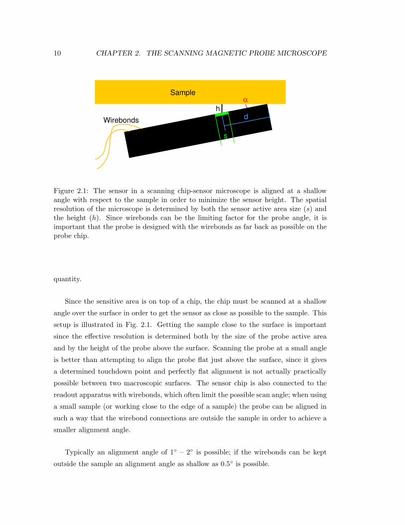
Figure 2.1: The sensor in a scanning chip-sensor microscope is aligned at a shallowangle with respect to the sample in order to minimize the sensor height. The spatialresolution of the microscope is determined by both the sensor active area size (s) andthe height (h). Since wirebonds can be the limiting factor for the probe angle, it isimportant that the probe is designed with the wirebonds as far back as possible on theprobe chip.
quantity.
Since the sensitive area is on top of a chip, the chip must be scanned at a shallow
angle over the surface in order to get the sensor as close as possible to the sample. This
setup is illustrated in Fig. 2.1. Getting the sample close to the surface is important
since the effective resolution is determined both by the size of the probe active area
and by the height of the probe above the surface. Scanning the probe at a small angle
is better than attempting to align the probe flat just above the surface, since it gives
a determined touchdown point and perfectly flat alignment is not actually practically
possible between two macroscopic surfaces. The sensor chip is also connected to the
readout apparatus with wirebonds, which often limit the possible scan angle; when using
a small sample (or working close to the edge of a sample) the probe can be aligned in
such a way that the wirebond connections are outside the sample in order to achieve a
smaller alignment angle.
Typically an alignment angle of 1 – 2 is possible; if the wirebonds can be kept
outside the sample an alignment angle as shallow as 0.5 is possible.

2.1. MICROSCOPE DESIGN 11
Figure 2.2: Photo of the scanning microscope mounted on the copper baseplate. Thesample is mounted directly on the baseplate. Wiring is heatsunk either using thesapphire stripline heatsink on the right-hand-side of the baseplate, or by wrappingaround copper bobbins such as the one visible in the back of the figure. Inset: Bottomview of the scanner with the probe mount mounted on the Z axis bender.
12 CHAPTER 2. THE SCANNING MAGNETIC PROBE MICROSCOPE
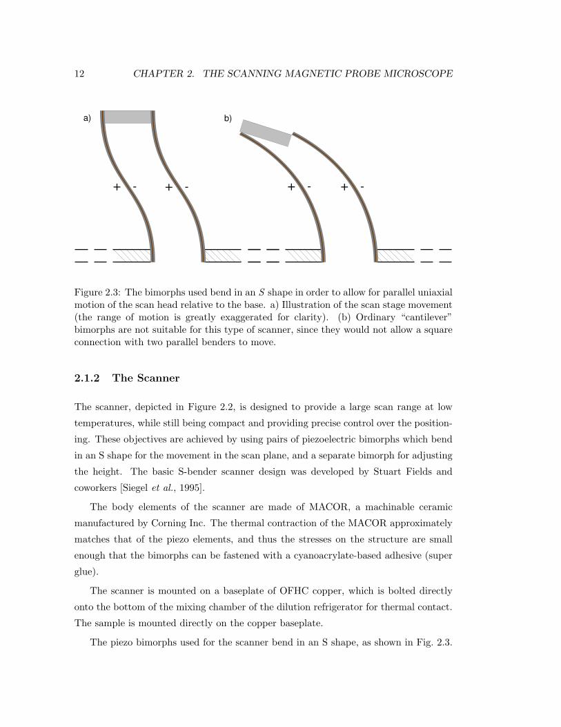
Figure 2.3: The bimorphs used bend in an S shape in order to allow for parallel uniaxialmotion of the scan head relative to the base. a) Illustration of the scan stage movement(the range of motion is greatly exaggerated for clarity). (b) Ordinary “cantilever”bimorphs are not suitable for this type of scanner, since they would not allow a squareconnection with two parallel benders to move.
2.1.2 The Scanner
The scanner, depicted in Figure 2.2, is designed to provide a large scan range at low
temperatures, while still being compact and providing precise control over the position-
ing. These objectives are achieved by using pairs of piezoelectric bimorphs which bend
in an S shape for the movement in the scan plane, and a separate bimorph for adjusting
the height. The basic S-bender scanner design was developed by Stuart Fields and
coworkers [Siegel et al., 1995].
The body elements of the scanner are made of MACOR, a machinable ceramic
manufactured by Corning Inc. The thermal contraction of the MACOR approximately
matches that of the piezo elements, and thus the stresses on the structure are small
enough that the bimorphs can be fastened with a cyanoacrylate-based adhesive (super
glue).
The scanner is mounted on a baseplate of OFHC copper, which is bolted directly
onto the bottom of the mixing chamber of the dilution refrigerator for thermal contact.
The sample is mounted directly on the copper baseplate.
The piezo bimorphs used for the scanner bend in an S shape, as shown in Fig. 2.3.

2.1. MICROSCOPE DESIGN 13
Figure 2.4: Sketch of the scanner. One pair of 2” long S-bender piezoelectric bimorphsconnect the scanner base to the secondary scan stage and provide motion in the Ydirection; a second pair connect the secondary and primary scan stages provide the Xaxis motion. A standard 1” cantilever bimorph provides the Z axis motion; the probemount is attached at the end of this bimorph. The scanner is mounted using threespring-loaded screws to a copper baseplate.

14 CHAPTER 2. THE SCANNING MAGNETIC PROBE MICROSCOPE
This can be accomplished using ordinary cantilever bimorphs, but segmenting the elec-
trodes in two pieces (typically by simply filing off a section of the electrodes at the
center of the bender) and applying opposite voltages on the top and bottom segments
of the piezo. More recently some manufacturers of piezo bimorphs have started manu-
facturing S-benders by poling the piezoelectric material in the two halves of the bender
in opposite directions.
The scanner, illustrated in Fig. 2.4 is constructed using two pairs of S-bender bi-
morphs. The first (Y ) connects the scanner base to the secondary stage, and the second
pair (X) connects the secondary stage to the primary stage. A cantilever bimorph (Z) is
mounted on the primary stage to provide height adjustment, and the sensor is mounted
at the end of this bimorph.
The S-bender scanner design intrinsically compensates for thermal contraction of the
piezos since the X and Y bimorph pairs are nominally identical; contraction of the pair
connected between the main scanner base and the secondary scan stage will decrease
the distance between the probe and the sample, while contraction of the bender pair
connecting the secondary and primary scan stages will increase that distance equally.
Thus any movement of the scanner because of thermal effects will mainly be caused
by the MACOR plates and the three mounting screws. The effect of this thermal
contraction is small, with the total contraction estimated to be about 25 µm, and
consistent enough between cooldowns that the Z adjustment range of around 25 µm at
low temperatures is large enough that the touchdown point consistently ends up well
within the piezo adjustment range after room temperature adjustment of the touchdown
point. This has allowed us to avoid any kind of low-temperature coarse approach
method, vastly simplifying the design.
While there is thermal compensation of the height, there is no such compensation
of motion in the X-Y plane, which may be caused by thermal contraction of the Z
bender. In addition, alignment of the sample with the sensor is done simply by moving
the sample around before fixing it in place with silver paint; typically a small dot of
thermal grease is used to hold the sample in place temporarily during the alignment
procedure. Because of these two significant limits on alignment accuracy, the scanner
is mainly useful for samples which do not demand precise alignment of the magnetic
probe with any particular point on the sample. Empirically we have found that the
interesting area should preferably be several hundred µm on a side in order to be easy

2.1. MICROSCOPE DESIGN 15
to align to at room temperature.
Since the flexibility of the scanner itself allowed us to avoid the complexity of any
low-temperature coarse motion, the scanner is mounted to the copper baseplate with
three screws surrounded by BeCu springs. This design allows for simple adjustment of
the height and the angle of the SQUID with respect to the sample, which is mounted
directly on the copper baseplate using silver paint as an adhesive in order to maximize
the thermal contact between the mixing chamber and the sample.
2.1.3 Sensor Mounting and Height Detection
In addition to being able to align the sensor with the sample, in order to scan the sensor
close to the surface it is essential to be able to determine when the SQUID is touching
the sample surface. In this microscope we have used a capacitive method of determining
when the sensor tip is touching the sample.
The sensor is mounted on a metal foil cantilever which in turn is mounted above
a Cu ground plane on a piece of circuit board, using a glass spacer (cut from a thin-
grade microscope coverslip) at the rear end of the cantilever. The capacitance depends
on the distance between the foil cantilever and the ground plane; modeling this as a
parallel-plate capacitor, the capacitance is inversely proportional to this distance. Thus
we can measure when the tip of the sensor touches the sample since the capacitor is
compressed. Alternatively, when scanning with the sensor touching the sample lightly,
the capacitance measurement gives a rough topographic map of the sample.
The noise level of the capacitance measurement is equivalent to movements of ap-
proximately 5 nm rms, and this sets the detection limit for which topographic features
can be detected while scanning in touching mode. However, when accurate detection of
the touchdown point is required other factors may be of importance, such as the type
of interaction between the tip of the sensor and the sample; e.g. a repulsive interaction
may smear out the touchdown point in the plot, while an attractive interaction may
cause the sensor to snap onto the surface.
The smallest possible sensor height is reached by scanning the sensor with the tip
touching the surface. This is not possible in all cases: some samples and/or sensors
are not robust enough for this (e.g. Hall probes are quite fragile); there may be a
concern that the sensor cannot be cooled to the same temperature as the sample and
heating must be avoided; or the sensor might produce spurious signals from touching
16 CHAPTER 2. THE SCANNING MAGNETIC PROBE MICROSCOPE
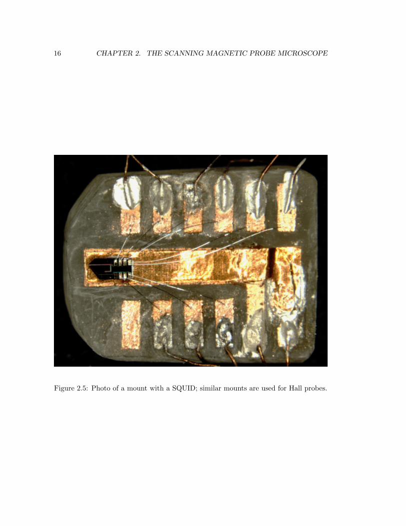
Figure 2.5: Photo of a mount with a SQUID; similar mounts are used for Hall probes.
2.1. MICROSCOPE DESIGN 17
the surface (in particular, Hall probes are typically somewhat piezoresistive, and this
effect can cause a local signal that is difficult to separate from a magnetic signal). In
this case, the sensor can be scanned in a plane above the sample, which is fitted by
doing touchdown measurements at the corners of the scan area. The height achieved
in this non-touching mode depends on how precisely the touchdown can be detected
and the smoothness of the surface; typically a height of less than 100 nm more than
the touching mode should be possible. The limit to touchdown detection is ideally the
noise level in the capacitance measurement. However, if there are interactions between
the probe and the sample, the probe may snap into the sample from some distance: in
order to achieve separation, the probe must be kept at a larger distance than this. The
snap-in also makes it more difficult to determine the exact touchdown point.
The metal foil used must be flexible enough that it allows the probe to deflect
without applying large forces at the tip of the probe, since hitting the surface too hard
might damage either the probe or the sample. The flexibility is determined by the foil
thickness and the elasticity of the foil material. We have found that in most cases,
if thin grades of metal foil are used (with a typical thickness of less than 25 µm),
the stiffness of the foil cantilever is smaller than that of the wirebonds between the
mount and the probe. Originally we used thin Al foil for the mounts; however, since
Al is superconducting below 1 K it is not suitable for use in a dilution refrigerator,
as it might disturb the magnetic fields and also has very low thermal conductivity
when it is superconducting. We anticipate that in some situations the probe is in fact
cooled mainly though the foil cantilever; this is especially likely if it is necessary to use
superconducting aluminum wirebonds, which have better adhesion properties than gold
wirebonds for some pad materials. In that case, it is of course of utmost importance that
the cantilever itself has high thermal conductivity. The obvious candidate material from
a thermal point of view is high-purity copper; however, copper is very easy to deform
plastically, leaving the cantilever crooked. Thin brass foil is a much easier material to
work with and appears to be a reasonable compromise.
2.1.4 Tunneling for Surface Detection and Topography Measurements
We have found that with the smallest Hall probes that we have made, where the active
area is less than 2 µm from the touching tip, the probes can easily be physically damaged
from touching down to use the capacitive touchdown measurement. In order to find

18 CHAPTER 2. THE SCANNING MAGNETIC PROBE MICROSCOPE
−12 −10 −8 −6 −4 −2 0 2−0.2
0
0.2
0.4
0.6
0.8
1
1.2
Distance from touchdown point [ µm]
∆C
[fF
]
Approach
Retraction
Sample
Sample
Figure 2.6: Capacitance measurement ramping the Z piezo voltage. At the touchdownpoint the capacitance starts changing rapidly. Only the deviation in capacitance fromthe non-touching value is measured.

2.2. GENERAL INSTRUMENTATION CONSIDERATIONS 19
the sample surface in a less harsh way we have attempted to use electrical tunneling
to detect the surface. Using this model, the voltage across the Z piezo is controlled
by a feedback circuit. For convenience we have used one of our SQUID controllers as
feedback circuit; in practice any PI regulating controller could be used for this purpose.
Ideally, one would be able to use this system in pure “STM mode”, constantly tunneling
from the Hall probe gate and following the surface topography by holding the tunnel
current constant. In practice this has turned out to be challenging since it appears that
the vibration level of the Z piezo is great enough that it is difficult to stay in tunneling
mode while scanning; often the probe ends up oscillating between touching the sample
and being far enough from the sample that the tunnel current is completely suppressed.
The main hurdle left in getting “STM mode” to work reliably is that the Z axis
vibration level must be improved. The situation was improved significantly when the
length of the Z bender was halved, but the improvement was not great enough to make
this detection system workable. It is possible that using a stiffer Z bender would be
sufficient; however, from the preliminary attempts involving a shorter piezo it appears
that the stiffness needs to be increased significantly. In an improved microscope with
coarse motion capabilities it may be feasible to rather drastically reduce the Z range
since it no longer needs to compensate for thermal drift during the cooldown.
2.2 General Instrumentation Considerations
2.2.1 Refrigeration
The dilution refrigerator used is a commercial Oxford Instruments Kelvinox 100, with
a base temperature specified to be below 15 mK. The cooling power is specified to be
at least 100 µW at 100 mK. The temperature is measured using a calibrated ruthenium
oxide resistance thermometer, measuring the resistance using the “Femtopower” control
unit built into the gas handling system. On installation, the thermometer was calibrated
against a 60Co nuclear orientation primary thermometer. The factory calibration of the
ruthenium oxide thermometer was determined to be accurate to within 1 mK down to
base temperature. The base temperature reached with no heat load was found to be
11 mK.

20 CHAPTER 2. THE SCANNING MAGNETIC PROBE MICROSCOPE
2.2.2 Magnetic and RF Shielding
To reduce stray magnetic fields, the refrigerator dewar is surrounded by a three-layer
cylindrical mu-metal shield with a triple-layer bottom. The shielding is designed to
reduce a lateral field by 81dB. The shielding specifications did not include a definite
specification of vertical field reduction. However, an order-of-magnitude reduction sim-
ilar to the lateral field shielding is reasonable. The residual magnetic fields that we
have seen in the microscope are inhomogeneous and large enough that they appear to
be caused by sources inside the refrigerator: typically the actual field at the sample
position with no field applied is a few tens of mG.
In order to avoid heating of the sample by radio frequency interference (RFI/EMI)
the entire system is enclosed in an RF shielded enclosure. The signal lines are passed
into the enclosure through a pass-through panel, where they are filtered using standard
low-pass π filters soldered into metal boxes.
2.2.3 Vibration Isolation
For any scanning microscope system, vibrations are an essential issue. The vibrations
of the probe must be significantly smaller than the resolution of the images taken. Since
the smallest sensor length scale that we are planning for is around 100 nm, vibrations
which are only a small fraction of that length scale, probably about 10 nm or less, will
not affect the measurements significantly. In order to achieve vibrational noise below
this level, the dewar hangs from a wooden tabletop which can be floated on optical
table legs. Vibrations entering through pumping lines are reduced by using flexible
bellows-style tubing and anchoring all the pumping lines rigidly at the wall of the RF
shielded enclosure and passing them through a concrete block.
We have characterized the vibrations at room temperature by using the piezo bi-
morphs as sensors, connecting a oscilloscope or spectrum analyzer to the electrodes;
this was done without actually floating the table, which is the mode in which the setup
has normally been used. The rms deviations measured in this way were approximately
0.75 nm in the X direction, 7.5 nm in Y, and 0.125 nm in Z. Turning on the pumps
increased the vibrational noise by less than a factor of 2. The lowest resonances of the
scanner are at 24 and 30 Hz in X, 26 and 30 Hz in Y, and 22 Hz in Z. While these
resonant frequencies are very low compared to smaller-range scanning microscopes, we

2.2. GENERAL INSTRUMENTATION CONSIDERATIONS 21
have in practice found the performance to be adequate for our sensors – we have never
been able to see any enhanced noise that could be traced to vibrations. In actual
measurements we have never found vibrations to be a limiting factor for the magnetic
sensitivity; as mentioned in Section 2.1.4, improved vibration levels are needed for run-
ning the instrument in STM mode for topography measurements.
There are several reasons why STM measurements are so much more sensitive to
vibrations than the magnetic probe measurements for which this microscope is designed.
First, the STM simply probes a much smaller length scale; since the magnetic sensors
used in this microscope average the signal over a much larger area, they are not very
sensitive to motion on a length scale which is small compared to the sensor size. Second
(but related) the working height of these sensors is large compared to that of an STM
tip; when scanning a sensor at an angle above a surface it is impossible to get it as
close as a tip pointing toward a surface (as an STM or AFM tip is). Since the fields
at the surface spread approximately as the distance from the surface, vibrations which
are small compared to the sensor height will not be problematic. Taken together, these
effects mean that vibrations of several nm are unlikely to cause any trouble for this
microscope, while an STM needs sub-Avibration levels for good (atomic-resolution)
results. Also, an STM intrinsically needs to operate at a low height even if the ultimate
resolution is not of interest, since the tunnel current is suppressed exponentially with
the tip-sample distance; this is essentially what gives STM its high-resolution properties
as well as its sensitivity to vibrations.
2.2.4 High-voltage amplifiers
The piezo benders are connected to high-voltage amplifiers. With piezo benders there
is no reason to keep one electrode at ground potential, so we apply symmetric voltages
with respect to ground to the two sides of the piezo benders. Using ±200 V (with
regard to ground) high-voltage amplifiers, we can thus apply up to ±400 V across the
piezo benders. This is not advisable at room temperature as the benders that we use
are specified for ±120 V at room temperature in order to prevent depoling. However, at
4K and below the benders do not appear to suffer any damage from the application of
significantly higher voltages. The cold dilution refrigerator environment also provides
a good vacuum which is important to avoid arcing when applying high voltages.

22 CHAPTER 2. THE SCANNING MAGNETIC PROBE MICROSCOPE
0 10 20 30 40 50 60 70 80 90 10010
−4
10−3
10−2
10−1
100
101
Frequency [Hz]
Vib
ratio
nal n
oise
den
sity
[nm
/Hz1/
2 ] X
Y
Z
Figure 2.7: Vibration spectra measured at room temperature by connecting the piezodriver lines to a spectrum analyzer. The Y piezo has larger vibrations than the others,presumably because the driven mass includes the mass of the X piezo bender pair.

2.3. EXPERIMENTAL POSSIBILITIES 23
2.2.5 Scan control system
The motion of the scanner is computer controlled, using 16-bit analog output boards
connected to the high-voltage amplifiers. The rastering does not need any feedback,
so no real-time computer control is necessary; however, for fast scanning hardware
triggering is used to synchronize the single-line voltage output and data readout. When
using tunneling touchdowns and feedback control, the feedback is done in a separate
analog feedback loop, with the tunneling output feeding back on the Z piezo voltage.
For these measurements the Z channel of the high-voltage amplifier was modified to
sum the inputs from the analog output board and the feedback control loop, so that an
offset plane can be applied in addition to using feedback for height control.
2.3 Experimental Possibilities
The experiments described in this thesis are mainly focused on superconductors, either
in thin-film or single-crystal form. However, the utility of this instrument is of course in
no way limited to superconductors. Given the materials focus of the rest of the thesis,
perhaps the most obvious extension is that there are materials other than superconduc-
tors which have an interesting magnetic structure on a length scale that we can access
using this instrument. Studying domain structure in magnetic materials is one example
that may be pursued.
Another category of measurements for which the instrument is suitable is studies of
mesoscopic systems, where electronic coherence effects are in some cases best studied by
non-invasive means such as measuring the magnetic field generated by currents in the
system. In this case, the scanner is used to position the probe over the sample, not for
imaging per se. One mesoscopic system which has seen extensive theoretical interest
and some experimental effort is persistent currents. The main interest in persistent
currents is that they offer a unique way of studying quantum coherence in an isolated
system: most other measurements related to quantum coherence effects, such as trans-
port measurements studying weak localization in metallic wires, must be performed
with the sample electrically connected to the outside world.
Persistent currents, periodic in the magnetic flux threading a phase coherent normal-
metal ring with a periodicity of hce , were originally predicted by Buttiker, Imry and
Landauer in 1983 [Buttiker et al., 1983]. In the simplest possible model – a metallic

24 CHAPTER 2. THE SCANNING MAGNETIC PROBE MICROSCOPE
loop without impurity scattering at T = 0 – the expected approximate magnitude of
the current is evF
L , where vF is the Fermi velocity and L is the circumference of the loop.
However, in a diffusive metallic loop, the expected current is reduced by a factor of lL
where l is the elastic mean free path. Thermal effects may further reduce the expected
currents [Chandrasekhar et al., 1991].
The first experiments on this subject were performed by Levy et al. on arrays of
copper rings [Levy et al., 1990]. The results somewhat surprisingly indicated that there
were persistent currents with a periodicity of hc2e , half of the expected period. This
was explained by averaging canceling out the hce component, which is expected to be
random in sign, but not the frequency-doubled component.
Chandrasekhar et al. measured the magnetic response of gold rings using SQUIDs,
with the rings fabricated directly on the SQUID. They found an hce response with an
apparent current magnitude that was significantly greater than the expected magnitude:
the predicted currents for the experimental parameters were well below 1 nA while the
measured peak currents had a magnitude of several nA [Chandrasekhar et al., 1991].
Later, Mailly et al. have studied ballistic GaAs/AlGaAs 2DEG rings in a similar way,
and found currents in good agreement with simple theories [Mailly et al., 1993]. Finally,
Jariwala et al. have measured the response of an array of 30 Au rings fabricated in
a SQUID pickup loop. These measurements appear to show he -periodic currents that
are significantly smaller than those measured in the earlier experiments [Jariwala et al.,
2001].
In the case of diffusive metallic rings, it appears that the experimental results are
somewhat contradictory, with question marks specifically because of the limited amount
of data available and the question of possible background signals. Both of these prob-
lems can be addressed by using a scanning probe microscope for measurements instead
of co-fabricating the samples and sensors. Being able to move between many samples in
a single cooldown allows many more samples to be used, and the ability to simply back
off from the sample and do a null measurement in order to test for background signals
is a much better background check than what could be performed for the metallic sam-
ples fabricated in the SQUID pickup loops. Furthermore, separating the sensor and the
sample allows for a much broader range of samples to be fabricated and measured since
the fabrication process does not need to be designed with not damaging the SQUID in
mind.

2.3. EXPERIMENTAL POSSIBILITIES 25
Since the rings that are typically discussed for these measurements have diameters on
a µm length scale, it is possible to use SQUIDs that are well matched to the sample size
in order to get maximal signal pickup. The magnetic flux from a 2 µm ring with a 4 µm
SQUID pickup loop placed 0.5 µm above the sample is approximately 0.6 µΦ0/nA.
A typical flux sensitivity for our SQUIDs is around 0.5 µΦ0/√
Hz at temperatures
below 1 K, giving a current sensitivity below 1 nA/√
Hz. SQUID noise is discussed
in more detail in Chap. 3. With this signal level, measuring currents on the level of
those reported by Chandrasekhar et al. should be relatively easy, and the theoretical
expectations of significantly sub-nA currents should be measurable with reasonable
amounts of averaging.

26 CHAPTER 2. THE SCANNING MAGNETIC PROBE MICROSCOPE

Chapter 3
SQUID sensors
As discussed in earlier chapters, many of the measurements reported in this thesis were
performed using Superconducting QUantum Interference Device (SQUID) sensors. This
chapter aims to first introduce SQUIDs as magnetic sensors, and then go into more
detail regarding the characteristics of the SQUIDs that we have used and participated
in developing.
We have used two different generations of SQUIDs. The first is a susceptometer
based heavily on Mark Ketchen’s original SQUID microsusceptometer [Ketchen et al.,
1984], which he and John R. Kirtley (both at IBM T.J. Watson Research Center)
modified for use in a scanning configuration [Kirtley et al., 1995; Gardner et al., 2001].
Aiming to improve on the characteristics of these SQUIDs as scanning sensors, we
have collaborated with Martin E. Huber on developing a new generation of SQUIDs
which have better noise characteristics and improved symmetry and shielding. We
have also started using a new high-bandwidth DC feedback system developed at NIST
which utilizes a SQUID series array as a low-temperature preamplifier, instead of the
traditional AC-coupled flux-locked loop control system.
3.1 SQUID Basics
SQUIDs are the most sensitive magnetic-field probes available, with flux sensitivities
as low as 0.1 µΦ0/√
Hz reported for experimental devices [Ketchen et al., 1991], where
the superconducting flux quantum Φ0 = hc2e = 20.7Gµm2.
Conceptually the SQUID consists of a superconducting ring with two Josephson
27
28 CHAPTER 3. SQUID SENSORS
junctions, which are breaks or weak links in the superconducting material. Cooper
pair tunneling is possible across this junction, but the critical current is much lower
than for the loop material. When a current larger than the junction critical current is
run through the SQUID, a voltage develops across the junctions. The voltage varies
periodically with the magnetic flux threading the loop.
The phase difference across a Josephson junction is governed by the Josephson
equations [Josephson, 1962],
Is = Ic sin γ and (3.1)
d(γ)
dt=
2eV
h(3.2)
where γ is the gauge-invariant phase difference
γ = ∆φ − (2π/Φ0)
∫
A · ds (3.3)
A real Josephson junction can be modeled by the “RCSJ model” - a Resistively and
Capacitively Shunted Junction [Tinkham, 1996]. The real junction is modeled as an
ideal Josephson junction in parallel with a resistor and a capacitor. Thus the current –
voltage relation for an RCSJ-model junction can be written as
I = Ic0 sin(γ) + V/R + CdV
dt(3.4)
A DC SQUID is simply a superconducting ring with two Josephson junctions in
parallel, illustrated in Fig. 3.1. For simplicity, we will consider a symmetric SQUID,
meaning that the two junctions are identical. With zero magnetic flux threading the
SQUID, there is equal current through both arms of the SQUID in this case. Thus
the phase difference across both junctions is identical and thus the condition that the
wavefunction is single-valued is satisfied.
When magnetic flux threads the loop, the wavefunction picks up a non-zero phase
from encircling the flux. In order to satisfy the condition that the wavefunction is single-
valued (and thus the phase change when encircling the loop is a multiple of 2π), there
must be an additional circulating current component which causes a phase difference
across the junctions. This causes a change in the voltage across the junctions. Since a
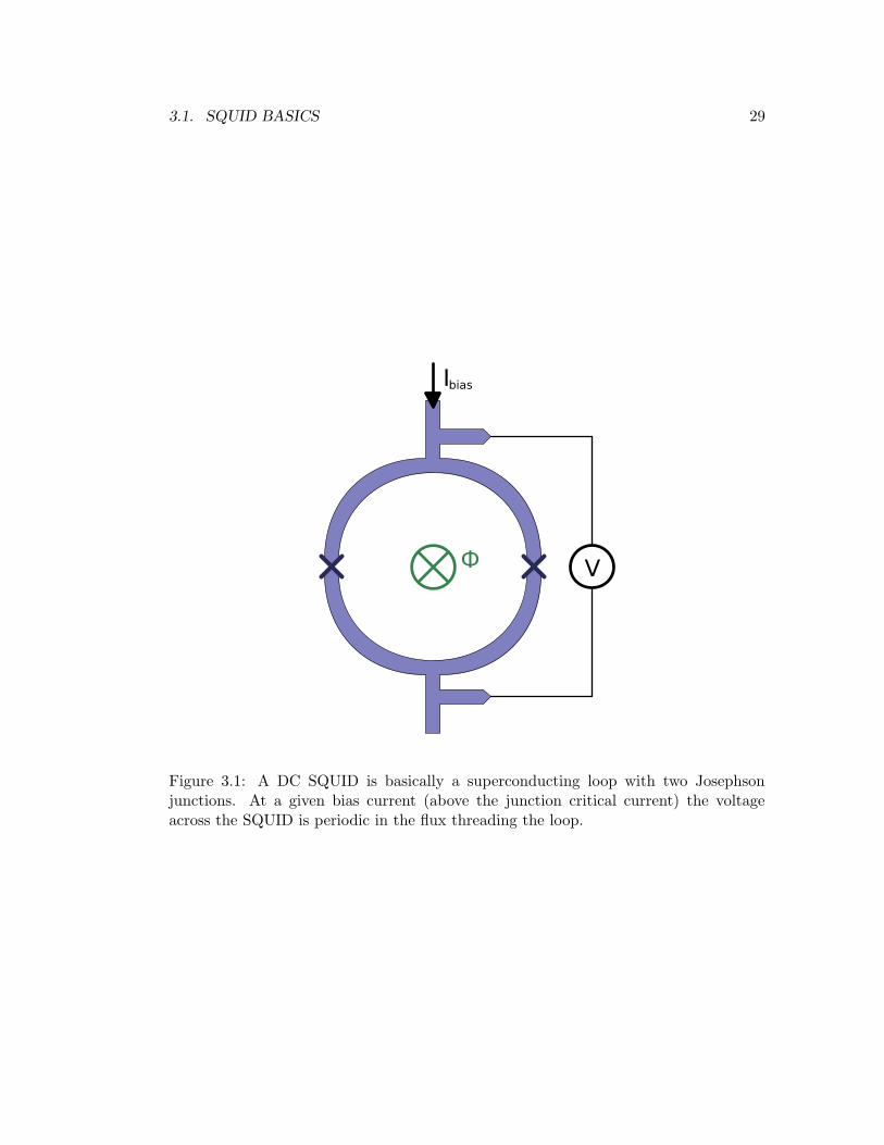
3.1. SQUID BASICS 29
Figure 3.1: A DC SQUID is basically a superconducting loop with two Josephsonjunctions. At a given bias current (above the junction critical current) the voltageacross the SQUID is periodic in the flux threading the loop.
30 CHAPTER 3. SQUID SENSORS
superconducting flux quantum through the SQUID gives exactly a phase contribution
of 2π, the voltage is periodic in the flux with a period of the flux quantum.
In order to linearize the signal, a feedback mechanism is used to always keep the flux
threading the SQUID at a specific value. Sample-caused changes in the flux threading
the SQUID are compensated by running a current through a modulation coil coupled
to the SQUID. The actual measured signal is the current through the modulation coil;
the deviation of this current from the base point value is proportional to the excess flux
though the SQUID. This description is only valid at low fields: at higher fields, flux
penetration into the superconductor diminishes the response.
A more in-depth description of the fundamental function of a SQUID can be found in
Tinkham’s “Introduction to Superconductivity” [Tinkham, 1996]. More technical dis-
cussion of SQUIDs and superconducting electronics can be found in “Superconducting
Devices and Circuits” by van Duzer and Turner [Van Duzer and Turner, 1998].
3.1.1 First-Generation Scanning SQUIDs: IBM Design
Our first generation of SQUID sensors were based on a design by Mark Ketchen [Ketchen
et al., 1984]. The initial design had two counterwound pickup loops connected symmet-
rically to the SQUID body, and lithographically patterned field coils surrounding the
pickup loops which could be used to apply a field locally to a small sample placed in
one of the pickup loops. When a field is applied by running a current through the field
coils when there is no sample, equal amounts of magnetic flux are passed through each
pickup loop. Since the loops are counterwound, i.e. oriented in opposite senses, the
net magnetic flux through the SQUID is zero if the SQUID is lithographically perfect.
Since this is never truly the case, there is a center tap between the field coils that allows
unequal currents to be run through the two coils; this capability is used to trim out
the imbalance. Thus any measured signal from applying a magnetic field with the field
coils will be caused by the magnetic response of a sample placed in one of the pickup
loops. The general design concepts for the SQUID susceptometers are illustrated in
Figure 3.2.
The design was modified for use in a scanning probe microscope by Mark Ketchen
and John Kirtley [Ketchen and Kirtley, 1995; Kirtley et al., 1995]. The major modifica-
tion of the original susceptometer design was to move one of the pickup loops far from
the main body of the SQUID, in such a way that the chip it was fabricated on could

3.1. SQUID BASICS 31
Figure 3.2: Sketch illustrating the fundamentals of Ketchen’s SQUID susceptometer.The two pickup counterwound pickup loops with surrounding field coils allow a magneticfield to be applied locally, only measuring the magnetic response of a sample placed inone of the pickup loops.
32 CHAPTER 3. SQUID SENSORS
be polished to a point close to that loop. In addition, the leads to the pickup loops are
fabricated as coaxial striplines in order to minimize the stray pickup area. This can be
done in a three-metal-layer lithography process.
The pickup loops in our first-generation SQUIDs were squares with a side of 8 µm,
and the field coils were octagons which are 21 microns across. The devices that we have
used were fabricated at the commercial superconducting electronics foundry HYPRES
based on our design files.
The tip could be polished to around 30 µm from the center of the pick-up loop;
the practical height of the pickup loop above the surface is thus generally limited to
around 2 µm: the height of the SQUID chip at the position of the pickup loop is
sin 3 × 30 µm ≈ 1.6µm and the pickup loop is covered by close to 0.5 µm of SiO2.
However, given the size of the pickup loop, this height generally does not limit the
resolution.
These SQUIDs have generally been run in a traditional AC flux-locked loop feedback
system, using a low-temperature transformer circuit to connect the SQUID to the room-
temperature electronics. This has the disadvantage of limiting the possible bandwidth
to a fraction of the lock-in frequency used; the frequency used in our IBM-designed
SQUID controller is 100 kHz, and this SQUID controller limits the bandwidth to around
400 Hz.
The first-generation SQUIDs we used were fabricated by HYPRES, a commercial
superconducting electronics foundry. The design files were provided by John Kirtley,
in some cases with minor modifications by us. The normal HYPRES process [Hypres,
Inc., As available online in June 2005] uses molybdenum (Mo) shunt resistors; this is not
suitable for use at dilution refrigerator temperatures since Mo is superconducting with
a Tc of 900 mK. This is obviously unfortunate since the “resistors” would then short out
the Josephson junctions at the temperatures which we are interested in working at. For
this reason, HYPRES did occasional runs with a different process using Pd/Au shunt
resistors which are non-superconducting. This process, for reasons entirely unrelated
to the shunt resistors, also used a lower critical current density in the junctions. This is
entirely unrelated to the change in shunt resistor material: it appears that some major
customers of the foundry needed a process with In order to accommodate for this we
increased the junction area for this set of SQUIDs; however it was kept small enough
to avoid issues related to the increased junction capacitance.

3.1. SQUID BASICS 33
Figure 3.3: a) A sketch of the design of our “first-generation” scanning SQUID design.b) Micrograph of the square front SQUID pickup loop, with a tip polished to a distanceof around 30 µm from the center of the pickup loop. The polishing distance is limitedby the octagonal field coil.
34 CHAPTER 3. SQUID SENSORS
10−1
100
101
102
103
104
100
101
102
Frequency [Hz]
Flu
x no
ise
dens
ity e
quiv
alen
t [Φ
0/sqr
t(H
z)]
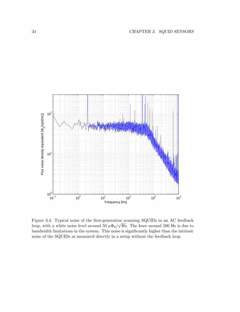
Figure 3.4: Typical noise of the first-generation scanning SQUIDs in an AC feedbackloop, with a white noise level around 50 µΦ0/
√Hz. The knee around 500 Hz is due to
bandwidth limitations in the system. This noise is significantly higher than the intrinsicnoise of the SQUIDs as measured directly in a setup without the feedback loop.
3.1. SQUID BASICS 35
The sensitivity (noise floor) of the first-generation SQUIDs using the AC feedback
electronics is about 50 µΦ0/√
Hz with the aforementioned bandwidth of less than 1 kHz
(varying with different measuring setups). A typical noise curve using this setup is
shown in Fig. 3.4. This relatively high noise level is an artifact of the measurement setup:
in other (non-scanning) setups we have measured the intrinsic noise of the SQUIDs to
be about 7 µΦ0/√
Hz.
3.1.2 Attempts to minimize the pickup loop area
Attempting to improve the spatial resolution of the first-generation SQUIDs, I modified
the design fabricated by HYPRES so that the pickup loop was replaced by a tab, as
illustrated in Fig. 3.5. The plan was to process the SQUIDs further at the Stanford
Nanofabrication Facility using e-beam lithography to pattern the tab into a sub-micron
pickup loop. The plan was ultimately unsuccessful and was abandoned for several
reasons, but several useful lessons were learned and the fabrication processes which
were developed may be useful for future developments.
The main reasons for abandoning the project were:
• Patterning the pickup loops turned out to be very challenging using the equip-
ment available at SNF. In particular, the e-beam writer available at the time, a
Hitachi HL-700, was not able to consistently reach the necessary feature sizes to
be useful. In addition, the machine was optimized for high-throughput processing
on wafers; unfortunately this impaired its functionality for processing small chips
significantly, in particular with respect to layer alignment - the machine often did
not detect the alignment marks on small samples and there was no good system
for manually aiding the alignment. Since this is a purely technical limitation it
can be overcome by using a different e-beam writer, such as the Raith 150 which
has now been installed at the SNF.
• The limits on the SQUID design set by the HYPRES fabrication process nec-
essarily forces a pickup loop with well-shielded leads to be fabricated close to
a large Nb area. This makes it practically impossible to avoid large amounts
of flux focusing into the pickup loop, giving a pickup area which is difficult to
characterize and much larger than the lithographically defined size [Ketchen and
Kirtley, 1995]. This would severely reduce the value of these probes for scanning

36 CHAPTER 3. SQUID SENSORS
Figure 3.5: Attempts to modify specially designed 1st-generation SQUIDs using e-beamlithography in order to produce submicron pickup loops. a) The regular 1st-generationSQUIDs have pickup loops fabricated using the HYPRES photolithographic process.Lithography limits set a practical lower bound on the pickup loop size of 8 µm. b) Thepickup loop was replaced by a tab in order to make e-beam lithography modificationspossible. c) Sketch of one attempted pickup loop geometry. d) Electron micrograph ofone of the attempts to fabricate the geometry in (c) that was closest to succeeding.
3.2. SECOND-GENERATION SQUIDS 37
microscopy. Similar SQUIDs could still be useful e.g. for studying individual
mesoscopic samples placed in the pickup loop.
• A further problem with integrating the HYPRES process with e-beam post-
processing is that there is no flexibility in the layer structure. Because of shielding
and other considerations, the pickup loop layer had to be fabricated in a layer
buried under around 0.5 µm of SiO2 This limits the attainable distance from the
sample surface to the pickup loop and diminishes the benefits of a small pickup
loop.
Given these problems we found it more fruitful to continue the work on smaller
SQUIDs in another direction: a different SQUID design, immediately developed with
scanning and small pickup loops in mind, which we have pursued in collaboration with
Martin Huber at CU Denver.
3.2 Second-Generation SQUIDs
In order to enable more sensitive SQUID measurements we have worked in collabo-
ration with Martin Huber at University of Colorado at Denver on a new generation
of SQUIDs with superior characteristics for scanning. The improvements are both in
an improved geometry, laying the groundwork for SQUIDs with significantly improved
spatial resolution, and in an improved flux noise level.
It is worthwhile to note that the size of the pickup loop is a very significant factor
not only for the spatial resolution but also for the spin sensitivity of the SQUID: if the
field is dipole-like, a large pickup loop will enclose very little net flux [Ketchen et al.,
1989].
While the experience from using the IBM-designed SQUIDs was important in guid-
ing the design of the new generation of SQUIDs, the design was done entirely from
scratch. The main design goals can be summarized as follows:
• Optimized for scanning. This implies, among other things, that there is a large
separation between the two field coils so that the rear pickup loop will be affected
as little as possible by the sample, and the wire bonds are placed at the rear end
of the SQUID so that they do not unnecessarily limit the angle at which the probe
can be scanned.
38 CHAPTER 3. SQUID SENSORS
• High symmetry. A symmetric design will tend to reduce spurious resonances in
the SQUID; this should reduce the noise level and make it much easier to work
with, since the SQUID is much less sensitive to small deviations from the ideal
operating point. A design that is symmetric with good precision also eliminates
or reduces the need for manual balancing of the current through the field coils.
This is very convenient in case the resistance of the wiring is not known to be
constant: in case the balancing is accomplished with a passive resistor network,
it is naturally sensitive to the wiring resistance. If no balancing is needed this
problem is overcome entirely, eliminating one possible source of measurement
errors. In addition, if the main body of the SQUID is “twisted” such that it has
equal pickup in opposite flux directions, a uniform background field will have little
effect on the SQUID, under some circumstances allowing operation in an applied
moderate background field.
• Possibility of integrating e-beam lithography steps. In order to achieve the goal
of small pickup loops, higher-resolution lithography than what is possible us-
ing small-scale optical lithography techniques is essential; line widths of around
100 nm would be necessary to reach the ultimate design goals. In order to do this
while keeping the fabrication process feasible it is essential to design the SQUID
in such a way that all the small features can be done in a few (preferably one)
electron-beam lithography step which can be integrated into the process flow.
Our current SQUIDs have been produced in a process using only optical lithography.
The smallest pickup loops fabricated in this process have had a diameter of 4 µm. The
NIST optical lithography process has design rules specifying line widths close to 1 µm;
in order to define well-formed pickup loops with a significantly smaller pickup area,
continuing work on integrating e-beam lithography (or some other higher-resolution
processing method) in the process will be necessary.
3.3 DC control loop for SQUIDs
Together with the second generation of SQUIDs we have used a new DC feedback system
originated by John Martinis and coworkers at NIST [Welty and Martinis, 1991]. Using a
DC feedback system allows operation at much higher frequencies, since one is no longer

3.3. DC CONTROL LOOP FOR SQUIDS 39
Figure 3.6: The 2nd generation scanning SQUID design. (a) A full SQUID chip with a4 µm pickup loop. (b) Close-up of the pickup loop area.

40 CHAPTER 3. SQUID SENSORS
−3−2
−10
12
3
−50
0
50
−100
0
100
200
Applied flux [Φ0]SQUID bias voltage [µV]
Cur
rent
thro
ugh
SQ
UID
[µA
]
Figure 3.7: Measured flux-voltage-current landscape for a second-generation SQUID at4K.

3.3. DC CONTROL LOOP FOR SQUIDS 41
bandwidth limited to a fraction of the AC chopping frequency of a traditional flux-
locked loop. A system bandwidth of 120 MHz has been experimentally demonstrated
using this type of feedback system [Huber et al., 2001].
In order to make DC feedback possible, low-temperature preamplification is nec-
essary; otherwise the impedance mismatch between the wiring and the SQUID would
make room-temperature readout impossible. The solution employed by Martinis et al.
is to use a series array of SQUIDs as a low-temperature current-to-voltage preampli-
fier. The modulation amplitude of the arrays is as large as several mV, and the output
impedance of a 100-SQUID array is reasonably well matched to standard coaxial trans-
mission lines: the typical output impedance is on the order of 1 Ω per SQUID in the
array and coaxial cables for cryogenic use are generally in the 50 – 100 Ω impedance
range. This minimizes problems with connecting the signal to the room-temperature
part of the feedback loop and allows for higher bandwidth.
The standard way to use the arrays is as a current preamplifier, using a room
temperature feedback circuit to linearize the signal. The feedback current, which is
applied to the array feedback coil, is proportional to the input current. Using this
feedback system means that the array is always operated at a constant flux bias point.
When using the arrays with a front end SQUID such as our scanning susceptometers,
the feedback current is instead fed into the feedback coil of the susceptometer SQUID,
as illustrated in Fig. 3.8. A constant current is applied to the SQUID array feedback
coil to bias it at a suitable fixed point.
In order to get a current signal from the front-end SQUID, it is operated in voltage-
biased mode instead of the current-biased mode that is commonly used with AC feed-
back mechanisms. The voltage biasing is accomplished by connecting a small resistor in
parallel with the SQUID and applying a bias current. The effective SQUID resistance
is typically limited by the shunt resistors to around 1 Ω, so the resistance of the parallel
resistor is much smaller than the SQUID resistance. Thus, when running a current
greater than the Josephson critical current through the SQUID, the voltage will be
held close to constant. Since the SQUID is also operated at a constant operating point
thanks to the flux feedback, the voltage biasing does not actually have to be perfect;
moderate non-linear effects will be compensated by the feedback, and thus the setup is
fairly insensitive to the precise value of the bias resistor or the relative resistance of the
bias resistor and the effective SQUID resistance.
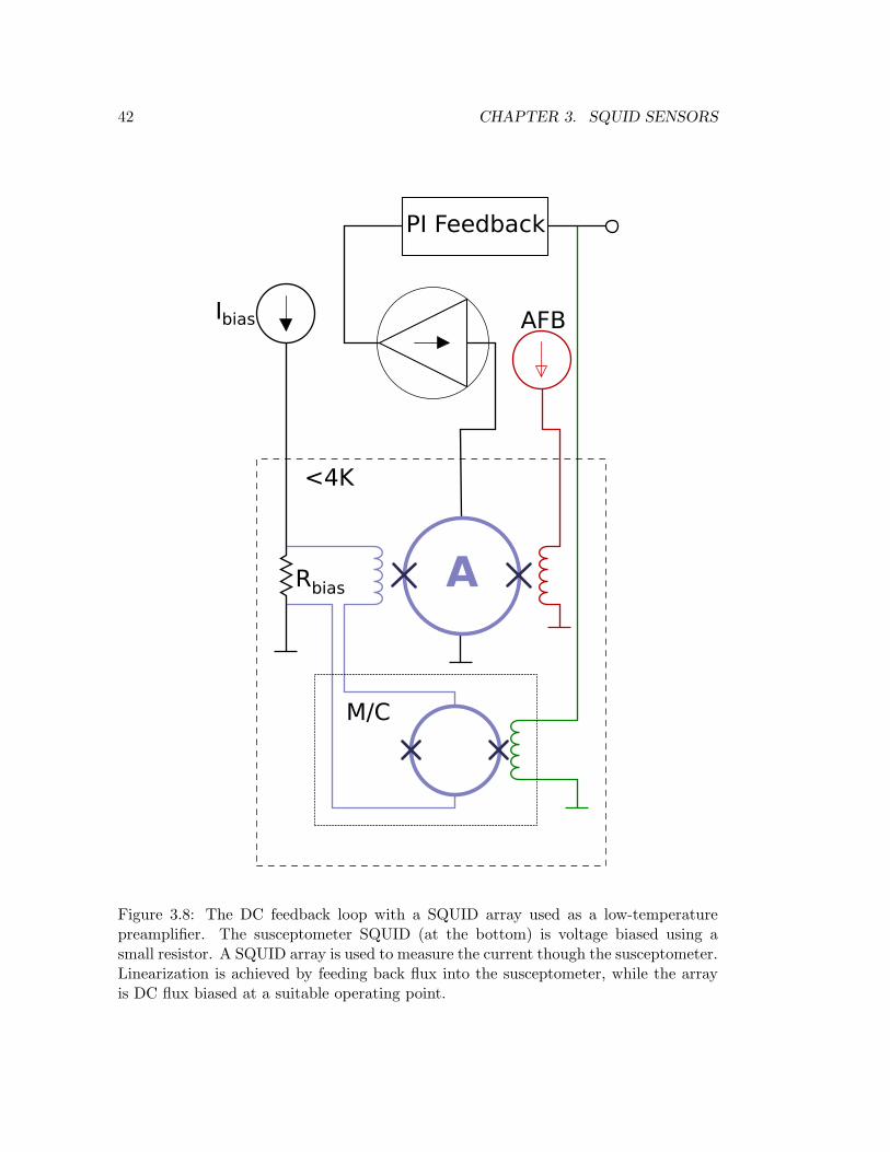
42 CHAPTER 3. SQUID SENSORS
Figure 3.8: The DC feedback loop with a SQUID array used as a low-temperaturepreamplifier. The susceptometer SQUID (at the bottom) is voltage biased using asmall resistor. A SQUID array is used to measure the current though the susceptometer.Linearization is achieved by feeding back flux into the susceptometer, while the arrayis DC flux biased at a suitable operating point.
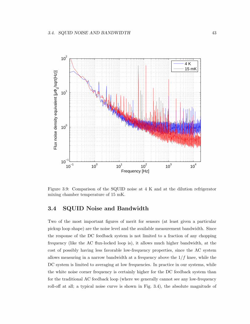
3.4. SQUID NOISE AND BANDWIDTH 43
10−1
100
101
102
103
104
10−1
100
101
102
Frequency [Hz]
Flu
x no
ise
dens
ity e
quiv
alen
t [µΦ
0/sqr
t(H
z)]
4 K15 mK
Figure 3.9: Comparison of the SQUID noise at 4 K and at the dilution refrigeratormixing chamber temperature of 15 mK.
3.4 SQUID Noise and Bandwidth
Two of the most important figures of merit for sensors (at least given a particular
pickup loop shape) are the noise level and the available measurement bandwidth. Since
the response of the DC feedback system is not limited to a fraction of any chopping
frequency (like the AC flux-locked loop is), it allows much higher bandwidth, at the
cost of possibly having less favorable low-frequency properties, since the AC system
allows measuring in a narrow bandwidth at a frequency above the 1/f knee, while the
DC system is limited to averaging at low frequencies. In practice in our systems, while
the white noise corner frequency is certainly higher for the DC feedback system than
for the traditional AC feedback loop (where we generally cannot see any low-frequency
roll-off at all; a typical noise curve is shown in Fig. 3.4), the absolute magnitude of
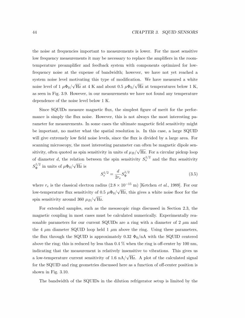
44 CHAPTER 3. SQUID SENSORS
the noise at frequencies important to measurements is lower. For the most sensitive
low frequency measurements it may be necessary to replace the amplifiers in the room-
temperature preamplifier and feedback system with components optimized for low-
frequency noise at the expense of bandwidth; however, we have not yet reached a
system noise level motivating this type of modification. We have measured a white
noise level of 1 µΦ0/√
Hz at 4 K and about 0.5 µΦ0/√
Hz at temperatures below 1 K,
as seen in Fig. 3.9. However, in our measurements we have not found any temperature
dependence of the noise level below 1 K.
Since SQUIDs measure magnetic flux, the simplest figure of merit for the perfor-
mance is simply the flux noise. However, this is not always the most interesting pa-
rameter for measurements. In some cases the ultimate magnetic field sensitivity might
be important, no matter what the spatial resolution is. In this case, a large SQUID
will give extremely low field noise levels, since the flux is divided by a large area. For
scanning microscopy, the most interesting parameter can often be magnetic dipole sen-
sitivity, often quoted as spin sensitivity in units of µB/√
Hz. For a circular pickup loop
of diameter d, the relation between the spin sensitivity S1/2s and the flux sensitivity
S1/2
Φ in units of µΦ0/√
Hz is
S1/2s =
d
2reS
1/2
Φ (3.5)
where re is the classical electron radius (2.8 × 10⁻¹⁵ m) [Ketchen et al., 1989]. For our
low-temperature flux sensitivity of 0.5 µΦ0/√
Hz, this gives a white noise floor for the
spin sensitivity around 360 µB/√
Hz.
For extended samples, such as the mesoscopic rings discussed in Section 2.3, the
magnetic coupling in most cases must be calculated numerically. Experimentally rea-
sonable parameters for our current SQUIDs are a ring with a diameter of 2 µm and
the 4 µm diameter SQUID loop held 1 µm above the ring. Using these parameters,
the flux through the SQUID is approximately 0.32 Φ0/nA with the SQUID centered
above the ring; this is reduced by less than 0.4 % when the ring is off-center by 100 nm,
indicating that the measurement is relatively insensitive to vibrations. This gives us
a low-temperature current sensitivity of 1.6 nA/√
Hz. A plot of the calculated signal
for the SQUID and ring geometries discussed here as a function of off-center position is
shown in Fig. 3.10.
The bandwidth of the SQUIDs in the dilution refrigerator setup is limited by the

3.4. SQUID NOISE AND BANDWIDTH 45
0 0.5 1 1.5 20
0.05
0.1
0.15
0.2
0.25
0.3
0.35
Offset of SQUID pickup loop from center of ring [µm]
Flu
x co
uple
d th
roug
h S
QU
ID [µ
Φ0 /
Hz1/
2 ]
Figure 3.10: Calculated magnetic coupling of ring of diameter 2 µm to a 4 µm diameterSQUID pickup loop 1 µm above the ring, as a function of the offset of the ring centerfrom the center of the pickup loop.
46 CHAPTER 3. SQUID SENSORS
wiring, not by the SQUIDs or the feedback system. The greatest limitation is in fact
not in the measurement system at all, but is caused by feeding the on-chip field coils
through twisted pair wiring, which limits the bandwidth for susceptibility measure-
ments to around 10 kHz. Improving the bandwidth to a few MHz should easily be
accomplished by only using coaxial wiring and making sure that there are no signifi-
cant impedance mismatches for all connections that need a broad frequency response.
For the measurements reported in this thesis this has not been necessary.

Chapter 4
Hall Probes
In addition to the SQUIDs described in the previous chapter, I have used Hall probes
as sensors for magnetic imaging. In this chapter I discuss Hall probe functionality and
the issues, primarily regarding noise and spatial resolution, to consider when using Hall
probes for scanning microscopy. In particular I discuss the noise properties of the Hall
probes used in the Moler lab.
Hall probes are magnetic field sensors based on the Hall effect. This effect is the gen-
eration of a transverse voltage across a conductor, proportional to the current through
the conductor, when it is subjected to a magnetic field.
The technique of using micro-Hall probes for microscopy was developed in the early
1990s, with significant contributions by the research groups of Chang and Hess [Chang
et al., 1992], Fields [Siegel et al., 1995] and Bending [Oral et al., 1996].
In the research reported in this thesis, four generations of Hall probes have been
used, generally with improved spatial resolution for each successive generation. The first
generation was fabricated by Kathryn Moler, the second generation by Janice Wynn
Guikema [Guikema, 2004], and the third and fourth generations by Clifford Hicks.
4.1 The Hall Effect
The basics of the Hall effect can be understood in terms of the Lorentz force. A moving
charged particle is subjected to a Lorentz force
~F = q( ~E + ~v × ~B) (4.1)
47
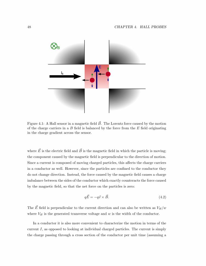
48 CHAPTER 4. HALL PROBES
Figure 4.1: A Hall sensor in a magnetic field ~B. The Lorentz force caused by the motionof the charge carriers in a B field is balanced by the force from the E field originatingin the charge gradient across the sensor.
where ~E is the electric field and ~B is the magnetic field in which the particle is moving;
the component caused by the magnetic field is perpendicular to the direction of motion.
Since a current is composed of moving charged particles, this affects the charge carriers
in a conductor as well. However, since the particles are confined to the conductor they
do not change direction. Instead, the force caused by the magnetic field causes a charge
imbalance between the sides of the conductor which exactly counteracts the force caused
by the magnetic field, so that the net force on the particles is zero:
q ~E = −q~v × ~B. (4.2)
The ~E field is perpendicular to the current direction and can also be written as VH/w
where VH is the generated transverse voltage and w is the width of the conductor.
In a conductor it is also more convenient to characterize the motion in terms of the
current I, as opposed to looking at individual charged particles. The current is simply
the charge passing through a cross section of the conductor per unit time (assuming a

4.2. HALL PROBE FABRICATION 49
rectangular slab conductor for convenience):
I = −nV qvtw (4.3)
where nV is the volume density of charges, t is the conductor thickness and w is the
conductor width. Thus for a thin flat slab Equation 4.2 turns into
nV tqVH = IB⊥ (4.4)
where B⊥ is the component of the magnetic field perpendicular to the conductor. Ex-
pressing the Hall voltage as a function of the magnetic field this is
VH =1
nV tqIB⊥. (4.5)
This equation shows that in order to achieve an appreciable Hall response, it is
important that the carrier density in the conductor is low, and ideally confined to as
thin a layer as possible in order to minimize the sheet carrier density nvt. In order to
achieve this, Hall probes are often fabricated in GaAs/AlGaAs heterostructures which
have a conduction layer of electrons confined to one of the GaAs/AlGaAs interfaces,
known as a “2-dimensional electron gas” (2DEG). At low temperatures the electronic
wavefunctions are confined to a single mode in the vertical direction. In this kind of
structure the volume density of electron is not a sensible parameter, instead the sheet
density (n) is the correct measure so the formula for the Hall effect turns into
VH =1
neIB⊥. (4.6)
There are also other factors beyond the Hall response that affect the signal to noise
ratio of a Hall probe. I will discuss Hall probe noise later in this chapter.
4.2 Hall probe fabrication
Our Hall probes are fabricated on GaAs/AlGaAs heterostructures, in which a 2DEG
forms at one of the GaAs/AlGaAs interfaces. The probes are defined by lithographic
patterning (using e-beam lithography for the probe areas of the sub-micron probes) and
reactive ion etching; the 2DEG is depleted and left non-conducting in the areas where

50 CHAPTER 4. HALL PROBES
the surface is etched.
The fabrication process is done in several steps. The probe area is defined first, with
e-beam and/or optical lithography and a shallow etch. The shallow etch is kept just
deep enough to deplete the 2DEG - a deeper etch would not allow as high resolution,
since there is a depletion region surrounding the physically etched area and a deeper
etch will cause a larger depleted 2DEG area. Contacts are made to the 2DEG using a
standard recipe using an annealed stack of AuGe/Ni/Au. The AuGe forms a eutectic
alloy which penetrates into the substrate and makes contact with the 2DEG through
the annealing process.
4.2.1 Scanning Hall probes
There are several special factors that need to be taken into consideration when Hall
probes are to be used for scanning probe microscopy. First, the probe is actually
sensitive to electric as well as magnetic external fields, since an electric field will have
a gating effect and cause a change in the electron density in the probe. In order to
avoid stray signal from e.g. charges on the surface, the sensor area can be protected
with a metallic gate that can be grounded in order to screen out external electric fields.
However, in this case care must be taken that the voltage between the gate and the
active area is small since otherwise the Hall probe may be depleted, and since there
may be current leakage between the gate and the probe if the voltage is too large.
A second concern is that the probes must be fabricated in such a way that they
can be brought close to the sample. Just as for the SQUIDs discussed in the previous
chapter, one necessary condition is that a tip can be polished on the Hall probe chip
such that the active area is very close to the corner. In general, this means fabricating
the Hall probes so that they can be polished to a tip close to the active area. However,
manual polishing is a difficult way to get the edge very close to the active area for two
reasons: First, it is simply difficult to polish the probes with micron-scale precision,
and second there is a risk of physical damage or introduction of defects that may cause
unpredictable depletion regions, possibly cutting off the active area entirely. Thus we
define a tip using a deep mesa etch, with a depth of several microns, using lithography
and etching techniques. The first-generation probes had a tip defined by wet etching;
this technique turned out not to be successful for the finer geometries attempted for
the later generations, e.g. due to undercutting of the resist when etching. In order to
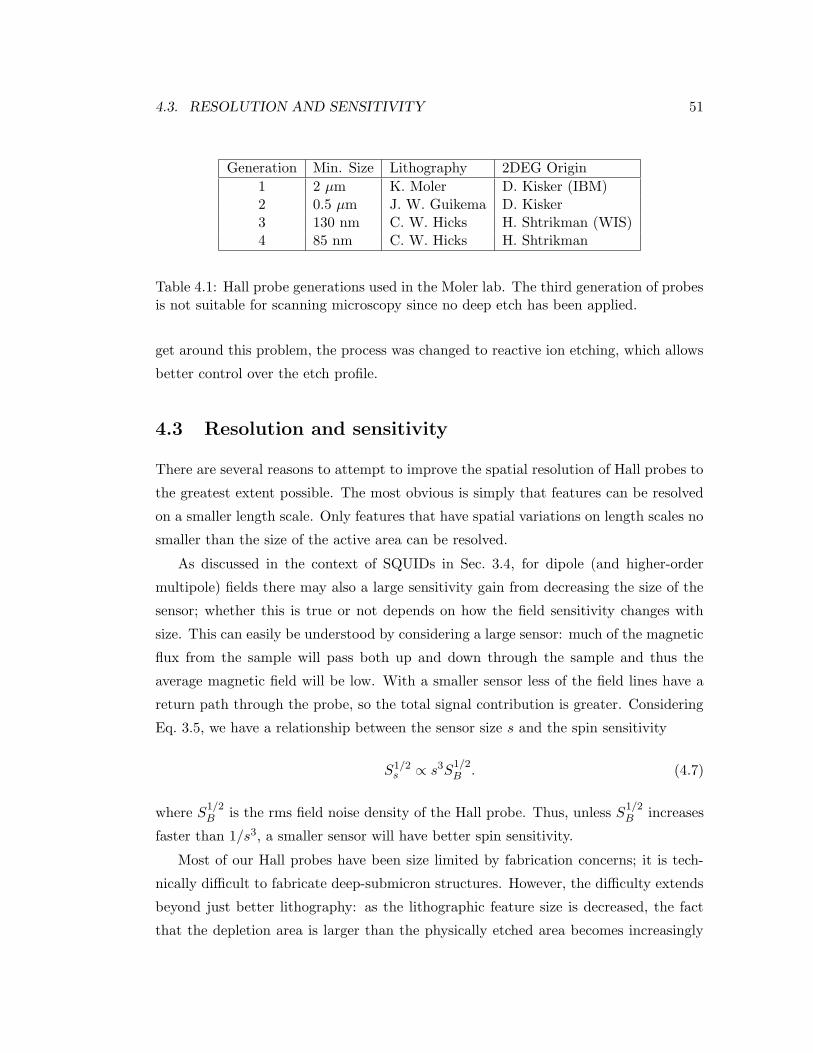
4.3. RESOLUTION AND SENSITIVITY 51
Generation Min. Size Lithography 2DEG Origin
1 2 µm K. Moler D. Kisker (IBM)2 0.5 µm J. W. Guikema D. Kisker3 130 nm C. W. Hicks H. Shtrikman (WIS)4 85 nm C. W. Hicks H. Shtrikman
Table 4.1: Hall probe generations used in the Moler lab. The third generation of probesis not suitable for scanning microscopy since no deep etch has been applied.
get around this problem, the process was changed to reactive ion etching, which allows
better control over the etch profile.
4.3 Resolution and sensitivity
There are several reasons to attempt to improve the spatial resolution of Hall probes to
the greatest extent possible. The most obvious is simply that features can be resolved
on a smaller length scale. Only features that have spatial variations on length scales no
smaller than the size of the active area can be resolved.
As discussed in the context of SQUIDs in Sec. 3.4, for dipole (and higher-order
multipole) fields there may also a large sensitivity gain from decreasing the size of the
sensor; whether this is true or not depends on how the field sensitivity changes with
size. This can easily be understood by considering a large sensor: much of the magnetic
flux from the sample will pass both up and down through the sample and thus the
average magnetic field will be low. With a smaller sensor less of the field lines have a
return path through the probe, so the total signal contribution is greater. Considering
Eq. 3.5, we have a relationship between the sensor size s and the spin sensitivity
S1/2s ∝ s3S
1/2
B . (4.7)
where S1/2
B is the rms field noise density of the Hall probe. Thus, unless S1/2
B increases
faster than 1/s3, a smaller sensor will have better spin sensitivity.
Most of our Hall probes have been size limited by fabrication concerns; it is tech-
nically difficult to fabricate deep-submicron structures. However, the difficulty extends
beyond just better lithography: as the lithographic feature size is decreased, the fact
that the depletion area is larger than the physically etched area becomes increasingly
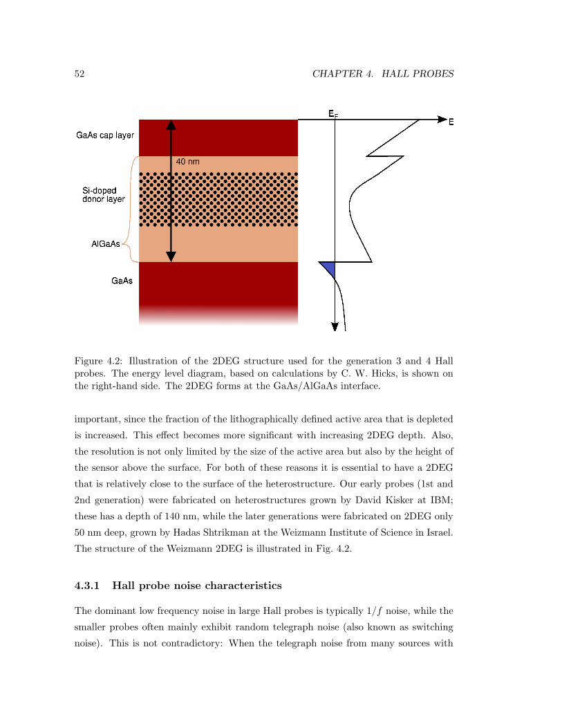
52 CHAPTER 4. HALL PROBES
Figure 4.2: Illustration of the 2DEG structure used for the generation 3 and 4 Hallprobes. The energy level diagram, based on calculations by C. W. Hicks, is shown onthe right-hand side. The 2DEG forms at the GaAs/AlGaAs interface.
important, since the fraction of the lithographically defined active area that is depleted
is increased. This effect becomes more significant with increasing 2DEG depth. Also,
the resolution is not only limited by the size of the active area but also by the height of
the sensor above the surface. For both of these reasons it is essential to have a 2DEG
that is relatively close to the surface of the heterostructure. Our early probes (1st and
2nd generation) were fabricated on heterostructures grown by David Kisker at IBM;
these has a depth of 140 nm, while the later generations were fabricated on 2DEG only
50 nm deep, grown by Hadas Shtrikman at the Weizmann Institute of Science in Israel.
The structure of the Weizmann 2DEG is illustrated in Fig. 4.2.
4.3.1 Hall probe noise characteristics
The dominant low frequency noise in large Hall probes is typically 1/f noise, while the
smaller probes often mainly exhibit random telegraph noise (also known as switching
noise). This is not contradictory: When the telegraph noise from many sources with

4.3. RESOLUTION AND SENSITIVITY 53
distinct switching rates and amplitudes is averaged, the resulting spectrum has a 1/f
characteristic. Similar behavior is seen in the 1/f noise found in devices such as silicon
FETs [Uren et al., 1985]. The source of the switching noise is believed to be changes in
the electronic configuration in the donor layer, which locally changes the potential in
the conduction layer.
The switching noise changes the resistance properties of the Hall probe. Thus it
is difficult to separate from the measured magnetic signal. The only possible way to
avoid the low-frequency noise when scanning is to scan quickly, process the averages
to reduce low-frequency noise (e.g. with line averaging, if that can be motivated - this
depends on the type of signal seen) and average many of the fast scans. This is quite
different from SQUIDs where the low-frequency noise is often less problematic and it is
possible to average for a long time in a single scan.
4.3.2 Noise data on our Hall probes
We have tested a range of Hall probes primarily designed for scanning applications.
The probe sizes have ranged from 80 nm to 10 µm. We have focused on characterizing
the size and temperature dependence of the Hall probe noise.
Since our main interest in Hall probes is using them in low-temperature systems,
we have focused on their low-temperature noise properties as well. In general, at low
frequencies our Hall probes have either a 1/f -like or somewhat bumpy noise profile.
At higher frequencies, the white noise floor has always been set by room-temperature
amplifier noise; our measurements have never been limited by intrinsic Johnson thermal
noise in a Hall probe at low temperatures. The voltage noise of our preamplifier is
4 nV/√
Hz, while at 4 K the Johnson noise of a Hall probe with a resistance of 1 kΩ
has a voltage noise density S1/2e =
√4kBTR ≈ 0.5nV/
√Hz.
At temperatures below 4 K there is very little temperature dependence of the noise.
However, the noise profile is quite sensitive to the bias current; this appears to indicate
that the noise typically is excited by the current, not by temperature. A comparison
of the noise measured at 4 K and at the dilution refrigerator base temperature in a
0.39 µm Hall probe is shown in Fig. 4.3.
The noise level is also completely insensitive to applied fields up to 100 G, as seen
in Fig. 4.4. This covers the field range generally used in our dilution refrigerator.
Assuming that noise sources in the 2DEG are localized and independent, the voltage

54 CHAPTER 4. HALL PROBES
noise density from the switching sites should add in quadrature and the total noise
density should be proportional to√
n, where n is the number of noise sources. If the
sources are distributed evenly in the active area of the probe, n should scale linearly
with the probe area, i.e. as s2 where s is the linear size of the Hall probe. If the
switching site is localized, the strength should be inversely related to the Hall probe
area. Thus the hall probe field noise in this model is expected to scale as 1/s.
A summary of the 10 Hz noise level for 11 Hall probes as a function of probe size
is shown in Figure 4.5. The noise was measured at the most favorable current for each
individual. The variation between individual probes is substantial, even between probes
of identical size. Since individual switching centers (as seen by characteristic switching
frequencies and amplitudes) are clearly identifiable in the time traces and spectra from
many of the smaller probes, some random variation even between nominally identical
probes is to be expected.
While the number of tested Hall probes is still too limited to draw any strong
conclusions. However, the general trend appears to be that the magnetic field noise
equivalent scales roughly as s−1.5. This is in disagreement with the 1/s agreement
argued for above; one possible explanation of the disagreement is that the switching
centers are concentrated at the edges of the probe active area, possibly caused by the
effects of the confining shallow etch. The size dependence in such a model may be more
complicated than the simple 1/s dependence of the pure area model; if only the corner
areas of the probes are considered, they need not scale at all with the size of the probe,
thus potentially giving a constant contribution to the number of noise sources. This
would give a 1/s2 contribution to the total noise level.
The Hall probes fabricated on the deeper IBM 2DEG (the “generation 2” probes)
appear to have significantly lower field noise for equivalent size than the generation 3
and 4 probes. This is consistent with the theory that the primary noise source is state
switching of two-level systems in the donor layer, since the greater distance means that
a change in the electronic configuration of the donor layer will cause a smaller potential
change in the deeper 2DEG. However, since a small size is essential both for spatial
resolution and spin sensitivity the shallow 2DEGs will be necessary for further work.

4.3. RESOLUTION AND SENSITIVITY 55
100
101
102
103
104
10−4
10−3
10−2
10−1
100
Frequency [Hz]
4 K
100
101
102
103
104
Frequency [Hz]
Hal
l res
ista
nce
nois
e [Ω
/Hz1/
2 ]
15 mK
4 µA
8 µA
12 µA
16 µA
20 µA
24 µA
28 µA
32 µA
36 µA
40 µA
Figure 4.3: Comparison of noise measurements on a 0.39 µm Hall probe at 4 K andat 15 mK dilution refrigerator temperature. The noise level at the two temperaturesis very similar. The only notable difference is that a two-level system with a charac-teristic frequency around 100 Hz appears to be triggered at lower currents in the 4 Kmeasurement.
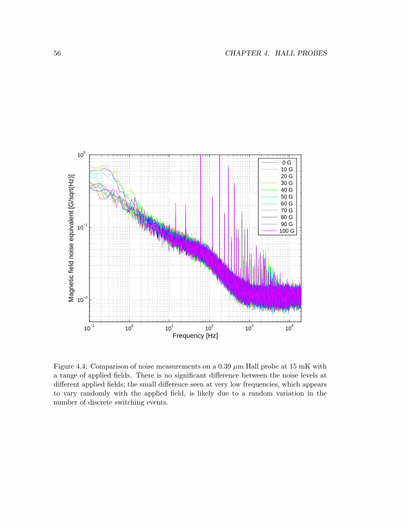
56 CHAPTER 4. HALL PROBES
10−1
100
101
102
103
104
10−2
10−1
100
Frequency [Hz]
Mag
netic
fiel
d no
ise
equi
vale
nt [G
/sqr
t(H
z)]
0 G 10 G 20 G 30 G 40 G 50 G 60 G 70 G 80 G 90 G100 G
Figure 4.4: Comparison of noise measurements on a 0.39 µm Hall probe at 15 mK witha range of applied fields. There is no significant difference between the noise levels atdifferent applied fields; the small difference seen at very low frequencies, which appearsto vary randomly with the applied field, is likely due to a random variation in thenumber of discrete switching events.

4.3. RESOLUTION AND SENSITIVITY 57
10−3
10−2
10−1
100
Fie
ld n
oise
at 1
0 H
z [G
/Hz1/
2 ]
0.1 1 10
10−4
10−3
10−2
Lithographic size of Hall probe [µm]
Flu
x no
ise
at 1
0 H
z [Φ
0/Hz1/
2 ]
Gen 2Gen 3Gen 4
Figure 4.5: Noise level at 10 Hz for Hall probes used in the Moler lab, at the measuredoptimal current for each probe. Generations are explained in Table 4.1. The noiseroughly appears to follow a power law. The fit is calculated using only the data forthe Gen. 3 and 4 Hall probes, since the Gen. 2 probes were fabricated on a different2DEG. The best fit for the field noise is 0.0305 × s−1.48; fits with the exponent forcedto -1 and -2 are represented by the dashed lines.

58 CHAPTER 4. HALL PROBES

Chapter 5
Local Magnetic Measurements on
Superconducting Thin Films
While the initial purpose of building the microscope described in this thesis was to
do measurements primarily on mesoscopic systems and on exotic materials (such as
Sr2RuO4, our measurements on which are described in Chapter 6), we have performed
a series of measurements that are in some sense “simpler” while optimizing the instru-
ment. These measurements have served both as a demonstration of the capabilities of
the instrument and as scientific measurements in their own right. In this chapter I will
describe some of these earlier measurements, their results and their implications.
5.1 Magnetic Susceptibility of Sn Disks
As an initial demonstration of the functionality of the scanner in a dilution refrigerator
environment, we studied the magnetic susceptibility of 3 µm diameter Sn disks, fabri-
cated in a square array with 30µm spacing, at temperatures down to 30mK. The sensors
used in these measurements were the Generation 1 SQUIDs with 8 µm square pickup
loops, as described in Chapter 3. A sketch of the measurement geometry - a dipole in
a square pickup loop - is shown in Fig. 5.1. The same sample had previously been used
for similar studies in another scanning SQUID susceptometer with a temperature range
down to 1.2 K[Gardner et al., 2001].
We applied a 200 Hz AC magnetic field by passing a 100 µA rms current throught
the on-chip field coils, producing a magnetic field of about 50 mG at the pickup loop.
59

60 CHAPTER 5. SUPERCONDUCTING THIN FILMS
Figure 5.1: A dipole in the 8 µm pickup loop of one of our Generation 1 SQUIDs. Theflux from the dipole through the SQUID must typically be calculated numerically whencomparing measurement results to theoretical models.
The magnetic response was measured using a lock-in amplifier.
Modeling the superconducting disk as a dipole and the SQUID pickup loop as a
square with a side of 8 µm, we could determine the scan height as well as the dipole
moment of the dot. The fitting method used was to calculate the least-squares fit of
the magnetic dipole moment at a given height.
The magnetic field from a dipole is
B(r) =µ0
4πr3(3(m · r)r − m) (5.1)
as discussed e.g. by Jackson [1999]. Since a SQUID measures the flux threading the
pickup loop, only the z component of the magnetic field will contribute to the mea-
surement. The z component of the magnetic field from a dipole in the z direction is
thus,
Bz =µ0M
4πr3
(
3z2
r2− 1
)
. (5.2)
The flux through a SQUID is the magnetic field integrated over the loop area. Since
dipole moment we are interested in is generated by the applied AC field, the relevant

5.2. SUPERCONDUCTING TRANSITION IN TUNGSTEN THIN FILMS 61
parameter is dm/dHaz. Thus the flux through the SQUID (modeled as a square with
a side s) from the dot is
Φs(r0) =µ0
4π
dmz
dHazHaz
∫ 1/2s
−1/2s
∫ 1/2s
−1/2s
(
3z2
r5− 1
r3
)
dxdy (5.3)
where r0 is the position of the center of the SQUID pickup loop relative to the dipole,
and r =√
(x − x0)2 + (y − y0)2 + z2. In general this integral must be computed nu-
merically.
In this case, the pickup loop was modeled as a square with a side of 8 µm. The
integral was computer numerically for a range of heights and the best-fit height was
chosen by minimizing the total least-squares error. For the disk shown in the suscepti-
bility obtained from the fit was dmz/dHaz = −5× 10⁷µB/G and the best-fit height was
1.9 mum. The susceptibility number is consistent with the susceptibilities measured on
disks on the same sample in previous experiments at around 2K; the measured values in
that experiment ranged from −3.5× 10⁻⁷ to −5.5× 10⁻⁷µB/G. A theoretical estimate
using the London model in the limit of zero penetration depth gives a predicted value
of the dipole moment of 7.9× 10⁻⁷ [Gardner et al., 2001]. The experimental results are
in reasonable agreement with the theoretical estimates given the rather simple model.
The moderate quantitative disagreement could be explained by a decreased response
caused by granularity of the dot material.
Apart from demonstrating the functionality of the scanner and the feasibility of
running it at low temperatures, these measurements demonstrate the power of the
scanning susceptometry technique for quantitative magnetic measurements mesoscopic
samples. This forms the basis on which experiments such as those proposed in Sec. 2.3.
5.2 Superconducting Transition in Tungsten Thin Films
In a second experiment, I have studied superconducting tungsten thin films using the
scanning SQUID susceptometer. These samples have specific technological relevance:
films identical to this one are normally used as photon detectors and energy sensors
(Transition Edge Sensors) for astrophysics experiments [Cabrera et al., 1998]. The sen-
sors used here have a transition temperature as measured in transport measurements of
146-148 mK, so by imaging this sample in the superconducting state we can demonstrate

62 CHAPTER 5. SUPERCONDUCTING THIN FILMS
−20 −10 0 10 20−2
−1.5
−1
−0.5
0
0.5
y [µm]
Φs [m
Φ0]
DataFit
5 µm
Figure 5.2: (a) Best fit of calculated SQUID response to data for a 3µm tin disk at30mK, height=1.9µm. (b) The corresponding full image, with the cross section markedwith a bright line.
the operating capabilities of the instrument in the 100mK temperature range.
The section of the sample that was within the scan range had a large area of thin
film W at the bottom. At the top of the images a set of Al rails, used for TES transport
measurements, can be seen. The rails are separated by an area of bare silicon, and the
top rail is comprised of two Al lines. At the very top of the images there is a small part
of a second W area. A sketch of the part of the sample corresponding to out scan area
is shown in Figure 5.3.
The Al current rails serve an important calibration purpose in the images. For
these measurements we could calculate the height of the pickup loop above the sample
by fitting the SQUID response to an applied background field with the tungsten in the
normal state, since there are two Al rails (one single-wire, the other two-wire) at the top
of the images. These are always superconducting in the temperature range of interest
and will thus be detectable by their diamagnetic response in an applied background
field.

5.2. SUPERCONDUCTING TRANSITION IN TUNGSTEN THIN FILMS 63
Figure 5.3: Sketch of the part of the W transition edge sensor visible in the scans.
5.2.1 Magnetometry: Vortex Imaging
The small remnant magnetic field in the dilution refrigerator, typically around 50 mG,
led to the trapping of magnetic flux vortices in the tungsten film on the transition
through Tc. I have imaged these vortices with magnetometry in order to study the
dynamics of vortex motion in the sample. Two series of consecutive images, taken at
30 mK and 120 mK, are shown in Fig. 5.4. Each image took approximately 15 min to
acquire; after one image was collected, the following scan was initiated immediately.
At 120mK the maximum flux from the vortices threading the pickup loop is only
around 10 mΦ0, indicating that the vortices are extremely spread out. This indicates
that the films are strongly in the thin-film limit, i.e. the penetration depth is much
greater than the thickness of the W film (40 nm). At 30mK the apparent penetration
depth is much smaller, as evidenced both by the greater contrast between the vortices
and the background, and the increased sharpness of the vortices seen. However, the
vortices are still broad and overlapping, making it very difficult to quantify the flux,
and impossible to quantitatively determine the penetration depth.
Sequential images sometimes show relatively large variations in the number and
placement of vortices. The vortices appear to be somewhat more likely to move at
100mK than at 30mK. However, even at the lowest temperatures reached the pinning
of the vortices is weak; while there are clearly a few preferred sites for vortices, the
vortices move quite freely between these sites, as indicated by the large changes between
consecutive images.
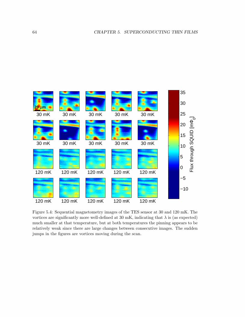
64 CHAPTER 5. SUPERCONDUCTING THIN FILMS
30 mK 30 mK 30 mK
30 mK 30 mK 30 mK 30 mK 30 mK
120 mK 120 mK 120 mK 120 mK 120 mK
120 mK 120 mK 120 mK 120 mK 120 mK
Flu
x th
roug
h S
QU
ID [m
Φ0]
−10
−5
0
5
10
15
20
25
30
35
30 mK
20 µm
30 mK
Figure 5.4: Sequential magnetometry images of the TES sensor at 30 and 120 mK. Thevortices are significantly more well-defined at 30 mK, indicating that λ is (as expected)much smaller at that temperature, but at both temperatures the pinning appears to berelatively weak since there are large changes between consecutive images. The suddenjumps in the figures are vortices moving during the scan.

5.2. SUPERCONDUCTING TRANSITION IN TUNGSTEN THIN FILMS 65
5.2.2 Low-Field Susceptometry
In addition to the magnetometry, I have performed low-frequency, low-field susceptibil-
ity measurements on the sample in a nominal temperature range between 30mK and
150mK. The field was applied using a 50µA rms current through the field coils, giving
a magnetic field of approximately 30 µG rms at the center of the pickup loop when no
sample is present. The output signal from the SQUID controller is measured using a
lock-in amplifier.
Up to 80mK there is no detectable decrease in the magnitude of the susceptibility of
the thin films. As the temperature is increased above 100mK the sample appears quite
inhomogeneous. The magnetic response of the sample decreases gradually until the
sample is entirely in the normal state at 140mK. The striking width of this transition
compared to transport Tc measurements on identical samples from the same wafer,
which typically show a transition width of less than 2mK, can be explained by the
fact that this measurement actually probes the penetration depth λ (or, essentially
equivalently, the superfluid density ρ) while the transport measurements simply probe
the initial formation of the superfluid condensate, at least in the low-current limit. Thus
magnetic measurements are a more sensitive probe of the details of the development of
the superfluid than transport measurements, while transport measurements are likely
a more accurate gauge of the zero-field Tc.
The thermal contact between the sample and the mixing chamber appears to be
good enough that the sample equilibrates at a given temperature as quickly as the
mixing chamber does, at least at temperatures above 100mK where the temperature
dependence of the susceptibility is obvious. This is demonstrated by the similarity of the
images taken while ramping the temperature up and down; no hysteresis is noticeable
to within less than 10 mK.
5.2.3 Susceptometry in a Background Field
In order to study the effect of a magnetic background field on the thin film we did sus-
ceptometry measurements similar to those described above but with DC offset current
applied to the field coils in addition to the AC excitation current, thereby measuring
λ(Hbackground). Images were taken in a range of different temperatures from 70 mK to
100 mK.

66 CHAPTER 5. SUPERCONDUCTING THIN FILMS
80 mK 90 mK 100 mK
110 mK 120 mK 130 mK 140 mK
Sus
cept
omet
ry s
igna
l [µΦ
0/µA
]
−100
−80
−60
−40
−20
0
70 mK
20 µm
Figure 5.5: Susceptibility images the TES film. The small-length-scale variations in thesusceptibility may be caused by the SQUID occasionally touching and locally heatingthe sample and may thus not be actual variations in the sample.
150 µA 300 µA 450 µA
150 µA 300 µA 450 µANo DC offset
100
mK
Sus
cept
omet
ry s
igna
l [µΦ
0/µA
]
−100
−80
−60
−40
−20
0
No DC offset
70 m
K
20 µm
Figure 5.6: Susceptometry images with a background field applied using the field coils.The applied AC current for the susceptometry is 50µA. The DC offset current thoughthe field coil is indicated on each scan.
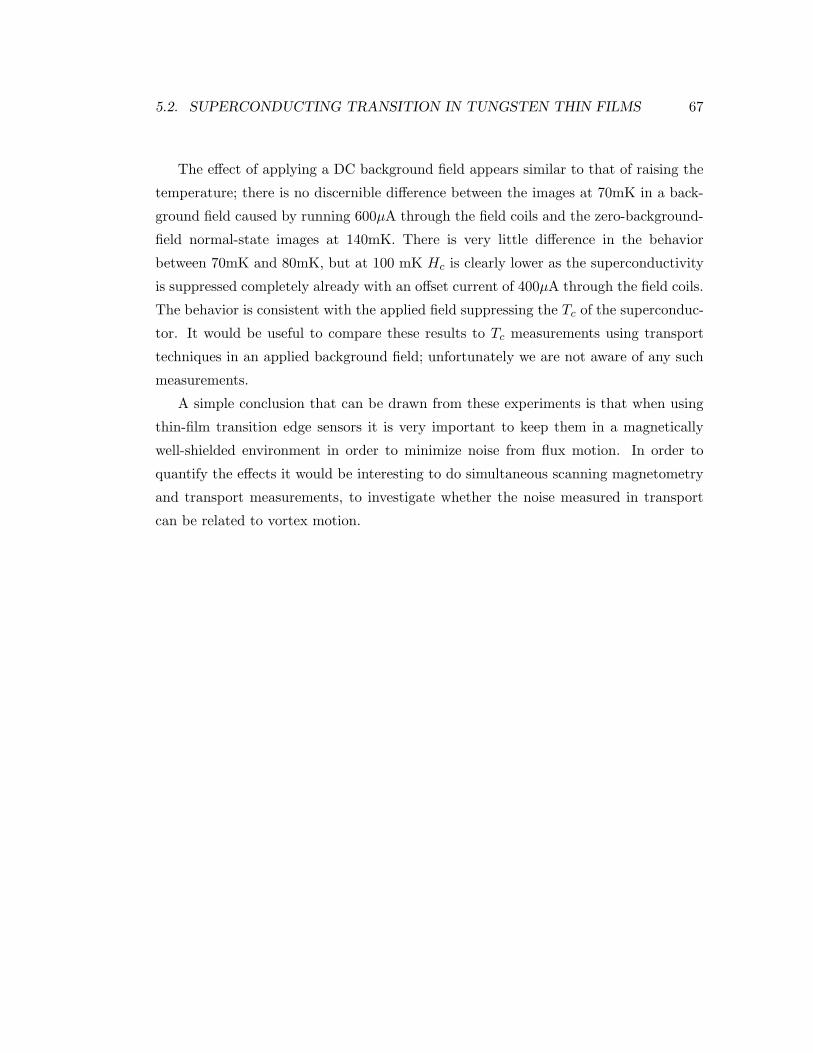
5.2. SUPERCONDUCTING TRANSITION IN TUNGSTEN THIN FILMS 67
The effect of applying a DC background field appears similar to that of raising the
temperature; there is no discernible difference between the images at 70mK in a back-
ground field caused by running 600µA through the field coils and the zero-background-
field normal-state images at 140mK. There is very little difference in the behavior
between 70mK and 80mK, but at 100 mK Hc is clearly lower as the superconductivity
is suppressed completely already with an offset current of 400µA through the field coils.
The behavior is consistent with the applied field suppressing the Tc of the superconduc-
tor. It would be useful to compare these results to Tc measurements using transport
techniques in an applied background field; unfortunately we are not aware of any such
measurements.
A simple conclusion that can be drawn from these experiments is that when using
thin-film transition edge sensors it is very important to keep them in a magnetically
well-shielded environment in order to minimize noise from flux motion. In order to
quantify the effects it would be interesting to do simultaneous scanning magnetometry
and transport measurements, to investigate whether the noise measured in transport
can be related to vortex motion.

68 CHAPTER 5. SUPERCONDUCTING THIN FILMS

Chapter 6
Search for Spontaneous
Time-Reversal Symmetry
Breaking in Sr2RuO4
In this chapter I describe a major part of my experimental work: studying the prop-
erties of the superconductor Sr2RuO4, in particular searching for signs of time-reversal
symmetry breaking (TRSB) using scanning SQUID and Hall probe microscopy.
These measurements have not resulted in any detection of magnetic signals that can
be understood in terms of TRSB. This appears to stand in contrast to the theoretical
estimates of the expected magnetic fields. However, there are still opportunities to
explain the results even for a TRSB superconductor, and I will discuss how to tie up
these loose ends with a combination of further theoretical and experimental work. A
brief account of these measurements has been published in a previous paper [Bjornsson
et al., 2005].
6.1 Sr2RuO4: A spin triplet superconductor
Strontium ruthenate, Sr2RuO4, has been studied extensively since its superconducting
properties were discovered in 1994 [Maeno et al., 1994]. Mackenzie and Maeno have
recently reviewed the experimental situation [Mackenzie and Maeno, 2003].
The material was the first non-cuprate superconductor with a layered perovskite
69

70 CHAPTER 6. SEARCH FOR TRSB IN SR2RUO4
structure to be discovered, eight years after the discovery of high-Tc in the cuprates.
There has been great effort, both experimental and theoretical, to identify the structure
of the energy gap [Mackenzie and Maeno, 2003].
Soon after the discovery of superconductivity in Sr2RuO4, it became clear that it had
unconventional properties. In particular, several strong pieces of evidence are available
for Sr2RuO4 being a spin-triplet superconductor, as opposed to the spin-singlet pairing
in both s- and d-wave superconductors.
The strongest early evidence for triplet pairing came from NMR Knight shift mea-
surements by Ishida et al. [Ishida et al., 1998]. The Knight shift directly measures the
spin susceptibility, which indicates the effective field at an atomic nucleus from the elec-
trons, and these measurements showed that the Knight shift was unchanged across the
superconducting transition. In an s-wave superconductor, the Knight shift is generally
expected to vanish in the superconducting state. The reason for this is that the Knight
shift is caused by spin polarization related to Zeeman splitting, and in a spin-singlet
superconducting state the condensate consists of Cooper pairs with zero spin. (This is
also related to one way a magnetic field can destroy superconductivity: when the energy
gained by forming the condensate is smaller than the Zeeman splitting, the condensate
is no longer energetically favored.) In contrast, a triplet pairing state where electrons
with equal spins are paired can exhibit a net polarization, just as the normal state.
Thus it is expected that for such a state the Knight shift will be unchanged when pass-
ing through the superconducting transition. This exactly matches the results of Ishida
et al. and is in general inconsistent with a singlet order parameter. However, there
are experimental counterexamples: Vanadium is an elemental s-wave superconductor
which also shows no change in the Knight shift across the superconducting transition
[Noer and Knight, 1964]. One possible reason other than a p-wave pairing symmetry
for a constant Knight shift is strong spin-orbit coupling [Anderson, 1959].
More recently, further and possibly more direct evidence for an odd-parity wavefunc-
tion, which requires triplet pairing, has been presented in the form of phase-sensitive
measurements by Nelson et al. [Nelson et al., 2004] They have fabricated SQUIDS
where they have connected opposite faces of Sr2RuO4 single crystals using the s-wave
superconductor InAu to complete the loop. By studying the magnetic flux dependence
of the SQUID, they have determined that the wavefunction undergoes a sign change
between opposite sides of the crystal. This type of SQUID is also known as a “π

6.1. SR2RUO4: A SPIN TRIPLET SUPERCONDUCTOR 71
SQUID” since the loop includes a spontaneous π phase shift. This is very strong evi-
dence for triplet pairing symmetry, since all singlet wavefunctions have the same sign
under mirror inversion.
6.1.1 Time Reversal Symmetry Breaking
In addition to being a triplet superconductor, there is some evidence that the wave
function is in fact a two-component time reversal symmetry breaking wavefunction.
The main experimentally detectable signature of a time reversal symmetry breaking
wavefunction is that there is a spontaneous current circulating around superconducting
domains, causing local magnetism. The main evidence for this to date is the µSR
(muon spin resonance) measurements by Luke et al. [Luke et al., 1998] µSR effectively
measures local magnetic fields in the sample, and they report a signal characteristic of
“a broad distribution of fields arising from a dilute distribution of sources”, concluding
that these localized magnetic fields are evidence for TRSB.
Further supporting evidence for a two-component order parameter comes from the
details of the flux lattice as observed by Kealey et al. with small-angle neutron scat-
tering [Kealey et al., 2000]. They find a square vortex lattice throughout the magnetic
field range where there is a vortex lattice which is generally not compatible with a
conventional superconductor, and the details of the magnetic field structure agree with
the predictions of a two-component Ginzburg-Landau model.
6.1.2 An explanatory cartoon of TRSB
TRSB can arise in superconductors where each Cooper pair carries a finite angular
momentum, and where the Cooper pairs are locked together with the same orientation,
as illustrated conceptually in Fig. 6.1. There may be domains with opposite orienta-
tion of the angular momentum vectors, conceptually similar to magnetic domains in a
traditional ferromagnet.
The magnetic moments are in this case caused by the orbital angular momentum
of the Cooper pairs. Internally in a domain the motion of neighboring pairs cancel out
and give no net current flow, but there is no such cancellation at the edge of a domain.
This leads to a net current within a coherence length of a domain edge, since ξ defines
the length scale of a Cooper pair.

72 CHAPTER 6. SEARCH FOR TRSB IN SR2RUO4
Figure 6.1: A cartoon for explaining the current flows and magnetic fields associatedwith TRSB in a superconductor with all electrons paired in L=1 Cooper pairs. Modelingthe pairs as orbiting electrons, in the interior there is no net current since neighboringelectron pairs cancel out; however, at an edge this cancellation is broken and there is acurrent within a distance ξ from the surface, flowing as indicated by the blue arrows.The magnetic field generated by this current is canceled by a counterflowing current onthe length scale of λ because of the Meissner effect.
However, since this is a superconductor magnetic fields are screened out through
the Meissner effect. The manifestation of the effect is that a screening supercurrent
flows in a region limited by the penetration depth λ, such that the field in the interior
of the domain is zero. This means that there are counterflowing currents on somewhat
different length scales around every domain.
6.1.3 The Order Parameter
A precise determination of the gap structure in Sr2RuO4 is yet another important com-
ponent in understanding the superconducting properties of the material. The issue
has been the subject of significant controversy, since thermodynamic probes such as
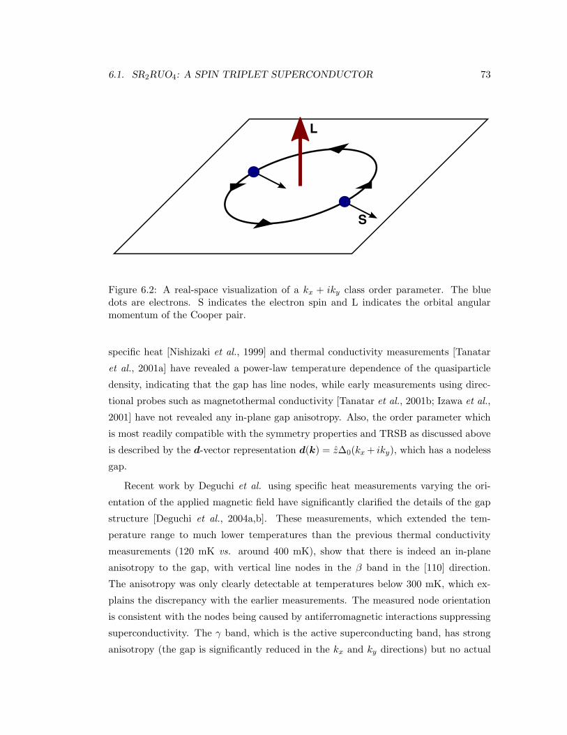
6.1. SR2RUO4: A SPIN TRIPLET SUPERCONDUCTOR 73
Figure 6.2: A real-space visualization of a kx + iky class order parameter. The bluedots are electrons. S indicates the electron spin and L indicates the orbital angularmomentum of the Cooper pair.
specific heat [Nishizaki et al., 1999] and thermal conductivity measurements [Tanatar
et al., 2001a] have revealed a power-law temperature dependence of the quasiparticle
density, indicating that the gap has line nodes, while early measurements using direc-
tional probes such as magnetothermal conductivity [Tanatar et al., 2001b; Izawa et al.,
2001] have not revealed any in-plane gap anisotropy. Also, the order parameter which
is most readily compatible with the symmetry properties and TRSB as discussed above
is described by the d-vector representation d(k) = z∆0(kx + iky), which has a nodeless
gap.
Recent work by Deguchi et al. using specific heat measurements varying the ori-
entation of the applied magnetic field have significantly clarified the details of the gap
structure [Deguchi et al., 2004a,b]. These measurements, which extended the tem-
perature range to much lower temperatures than the previous thermal conductivity
measurements (120 mK vs. around 400 mK), show that there is indeed an in-plane
anisotropy to the gap, with vertical line nodes in the β band in the [110] direction.
The anisotropy was only clearly detectable at temperatures below 300 mK, which ex-
plains the discrepancy with the earlier measurements. The measured node orientation
is consistent with the nodes being caused by antiferromagnetic interactions suppressing
superconductivity. The γ band, which is the active superconducting band, has strong
anisotropy (the gap is significantly reduced in the kx and ky directions) but no actual

74 CHAPTER 6. SEARCH FOR TRSB IN SR2RUO4
nodes. The gap structure of the γ band can be explained by the TRSB order parameter
described by d(k) = z∆0(sin(akx) + isin(aky)). This gap structure, with nodes in the
β band and a γ band gap belonging to the kx + iky class, is consistent with the full
body of experimental data on the gap structure of Sr2RuO4.
A real-space visualization of a kx + iky class order parameter is shown in Fig. 6.2.
The spins of the two electrons forming a pair are parallel and their orientation is locked
to the ab plane of the material, with the orbital moment L of the pair aligned with the
c axis.
6.2 Detecting TRSB Using Local Magnetic Measurements
One of the most dramatic consequences of the order parameter described above is its
time-reversal symmetry breaking (TRSB) nature. This can be probed by measuring
local magnetic fields in the sample. An experiment that can directly probe the spatial
distribution of the expected spontaneously generated magnetic fields is one of the last
missing pieces in the puzzle of the Sr2RuO4 wavefunction. We have sought to perform
just such an experiment.
There are three magnetic signatures of TRSB that could be observable by local
magnetic imaging:
Edge currents. In a single crystal with no domains (e.g., the order parameter
throughout the crystal would be either kx + iky or kx − iky), there should be an edge
current within a coherence length of the edge, and a counter-circulating shielding cur-
rent within a penetration depth [Sigrist and Ueda, 1991; Kwon et al., 2003]. Kwon et
al. argued that in Sr2RuO4, this effect would produce a net magnetic flux of 2.6 Gµm
per unit length of the edge [Kwon et al., 2003]. These calculations do not take the pos-
sibility of chiral domains into account; they assume a single chiral domain which is large
compared to the measurement device. In order to make more accurate predictions, full
Maxwell-London calculations taking the domain size into account may be necessary.
Currents at domain walls. Matsumoto and Sigrist argued that domains are ener-
getically unfavorable, and are only found because of domain wall pinning [Matsumoto
and Sigrist, 1999]. In principle the domain size may range from the sample size to the
coherence length, ξab = 66 nm. Very different patterns of current flow would result
depending on whether the domains are smaller or larger than the penetration depth,

6.2. DETECTING TRSB USING LOCAL MAGNETIC MEASUREMENTS 75
λab ≈ 160 nm. We are not aware of quantitative theoretical predictions on the expected
magnetic signal from domain walls. Kwon et al. actually mention domain walls as
a source of magnetic fields, but merely note that there should be no net flux from a
domain wall, and thus they are not likely to be detectable using a SQUID because all
current SQUIDs are large compared to the relevant length scales of field cancellation
(λ and ξ).
Defects. Currents with counter-circulating shielding currents are also expected to
flow around defects.
In previous work, Tamegai et al. studied local magnetization at the edge of a
sample using a stationary 5×5µm2 Hall probe [Tamegai et al., 2003]. They detected
no spontaneous magnetic fields associated with edge currents, although they did report
anomalies in the magnetization hysteresis loops that they suggest indicate the presence
of chiral domains.
Simultaneously with the work reported in this thesis, Dolocan et al. has reported
observing coalescing vortices forming flux domains. They suggest that this observation
indicates the presence of topological defects such as domain walls resulting from uncon-
ventional chiral superconductivity [Dolocan et al., 2004]. However, they did not detect,
nor were they explicitly looking for, magnetization signals from edges and defects.
I have improved on the earlier experiments in the field primarily by improving the
magnetic field sensitivity by using smaller and/or more sensitive probes, and by imaging
a sample specifically patterned to provide a detectable signal.
6.2.1 Samples
The pure Sr2RuO4 samples used were single crystals, grown by the research group of
Yoshi Maeno utilizing a floating-zone method [Mao et al., 2000]. Tc as determined by
bulk AC susceptibility measurements on pieces from the same crystal bar was 1.422 K
(transition midpoint) with a transition width of 24 mK; this agrees with the less precise
observations of Tc – close to 1.5 K – in our scanning measurements. The temperature
measurement in the scanning experiments is more coarse-grained since I focused on
imaging the sample at a set of different temperatures as opposed to carefully following
the temperature dependence at a single point; since imaging the sample takes a sig-
nificant amount of time, and the temperature must be stable during a scan (implying
that the refrigerator must be stabilized at the temperature before the measurement is

76 CHAPTER 6. SEARCH FOR TRSB IN SR2RUO4
Figure 6.3: An SEM image of the Sr2RuO4 crystal used for the Hall probe imaging. Anarray of holes was milled in the sample using a FIB. The hole spacing is 20 µm.
started), it is not feasible – and generally not particularly interesting – to collect imag-
ing data spaced as closely in temperature as would be typical for a bulk susceptibility
measurement.
The first imaged sample was imaged as-cleaved without any further processing. It
was scanned with a SQUID sensor with a 4 µm pickup loop. I prepared a second sample
by patterning a cleaved crystal with an array of approximately 1 µm diameter pits with
a spacing of 20 µm using a Focused Ion Beam (FIB) with 30 kV acceleration voltage
of Ga+ ions. The depth of the pits is estimated to be around 1 µm; however, for a
precise measurement of the depth the sample would have to be sliced apart e.g. with
an FIB. Since this would destroy the sample I have not done so at this point in time.
An SEM image of this sample is shown in Figure 6.3. Each sample was mounted in
silver epoxy and connected to the mixing chamber baseplate of the dilution refrigerator
with a copper wire for thermal contact.

6.2. DETECTING TRSB USING LOCAL MAGNETIC MEASUREMENTS 77
10 µm0
0.02
0.04
0.06
0.08
0.1
0.12
0.14
0.16
0.18
0.2
0
0.02
0.04
0.06
0.08
0.1
0.12
0.14
0.16
0.18
0.2
Flu
x th
roug
h S
QU
ID p
icku
p lo
op [Φ
0]
0
0.05
0.1
0.15
0.2
Figure 6.4: Scanning SQUID image of a single crystal of Sr2RuO4 with a single vortexwithin the field of view. The only other magnetic signals visible are a smoothly varyingbackground.
6.2.2 SQUID Imaging of an As-Cleaved Crystal
SQUID images of an unpatterned sample were acquired at a height of approximately
2 µm above the sample surface. The most prominent feature in most images were mag-
netic vortices. These all appeared completely conventional, carrying 1 Φ0 of magnetic
flux to within calibration errors which may be on the order of 10%. An image with a
single vortex is shown in Fig. 6.4.
In images where the background field was carefully compensated, so that there were
no vortices in the field of view, shown in Fig. 6.5, we detected a smoothly varying
background and a few dipole-like artifacts that were present even at 4 K and thus must
be unrelated to the superconductivity of the Sr2RuO4 sample. The smooth background
may be caused by pickup from a secondary pickup loop, which was extended over the
edge of the sample. The total magnitude of the background variation is on the order
of 50 mG, and the noise level in the measurements, measured as the rms difference
between adjacent pixels with 0.6 µm spacing, is 0.45 mG (equivalent to approximately
0.4 mΦ0 rms flux noise).

78 CHAPTER 6. SEARCH FOR TRSB IN SR2RUO4
10 µm
a)
Flu
x th
roug
h S
QU
ID p
icku
p lo
op [Φ
0]
0
0.05
0.1
0.15
0.2
10 µm
b)
Flu
x th
roug
h S
QU
ID p
icku
p lo
op [m
Φ0]
0
5
10
15
20
Figure 6.5: Scanning SQUID image of the same area of a Sr2RuO4 crystal as in Fig. 6.4but with the background field compensated so that there are no vortices. In (a), thecolor scale is the same as for Fig. 6.4, while (b) is the same image with the color scalestretched to enhance detail. The only visible features apart from the smooth background(which may be caused by the secondary pickup loop hanging off the sample) are dipole-like structures that are visible both in the superconducting and normal state (measuredat 4 K) and thus appear to be magnetic particles stuck on the surface.

6.2. DETECTING TRSB USING LOCAL MAGNETIC MEASUREMENTS 79
For a sensor of this size, the flux at an edge through the sensor predicted by Kwon
et al. [Kwon et al., 2003] is around 0.5 Φ0. The scanned area did not include any sharp
edges; however, there were shallow steps within the scan area which should to some
extent be similar to edges. In order to make detailed predictions of the signal level,
significantly more detailed calculations which take the geometry into account would be
necessary.
6.2.3 Hall Probe Imaging of a Hole-Array Sample
The next experiment used a Hall probe with an active area of 0.5 µm×0.5µm to image
a crystal with FIB-milled holes (Figure 6.3). This experiment had three improvements
that allow the data to be compared semi-quantitatively with theory. First, the FIB-
milled holes provide edges throughout the imaged area. Second, the Hall probe has
only a single active area and therefore does not suffer the same systematic background
errors. Third, the Hall probe has a smaller active area than the SQUID and can be
scanned at a lower height, providing higher spatial resolution.
A low-field Hall probe scan of the sample is shown in Figure 6.6. The image is
completely free of features other than a few isolated trapped vortices, such as commonly
appear in low-field, low-temperature magnetic scans of type-II superconductors. These
vortices appear to be entirely conventional, carrying a magnetic flux of h2e within 10%
error, as determined by integration of the measured local magnetic field. The apparent
lateral extent and shape of the vortices is limited by the sensor scan height. Fits to
these images of isolated individual vortices determine the probe height to be 1.2±0.2µm
above the surface. Thus our spatial resolution is limited by the height of the probe above
the surface, not the probe size itself [Kirtley et al., 1999].
The dominant noise source in these measurements is Hall probe 1/f noise. To
minimize this noise, we used the standard scanning microscopy technique of scanning
relatively quickly (2 s/scan line) and averaging multiple scans, subtracting the back-
ground level of each line and removing sudden jumps. For the image in Figure 6.6, 80
scans were averaged. The resulting background noise has an rms value of 35 mG, with
no sign of the array of holes milled in the sample or any other features.
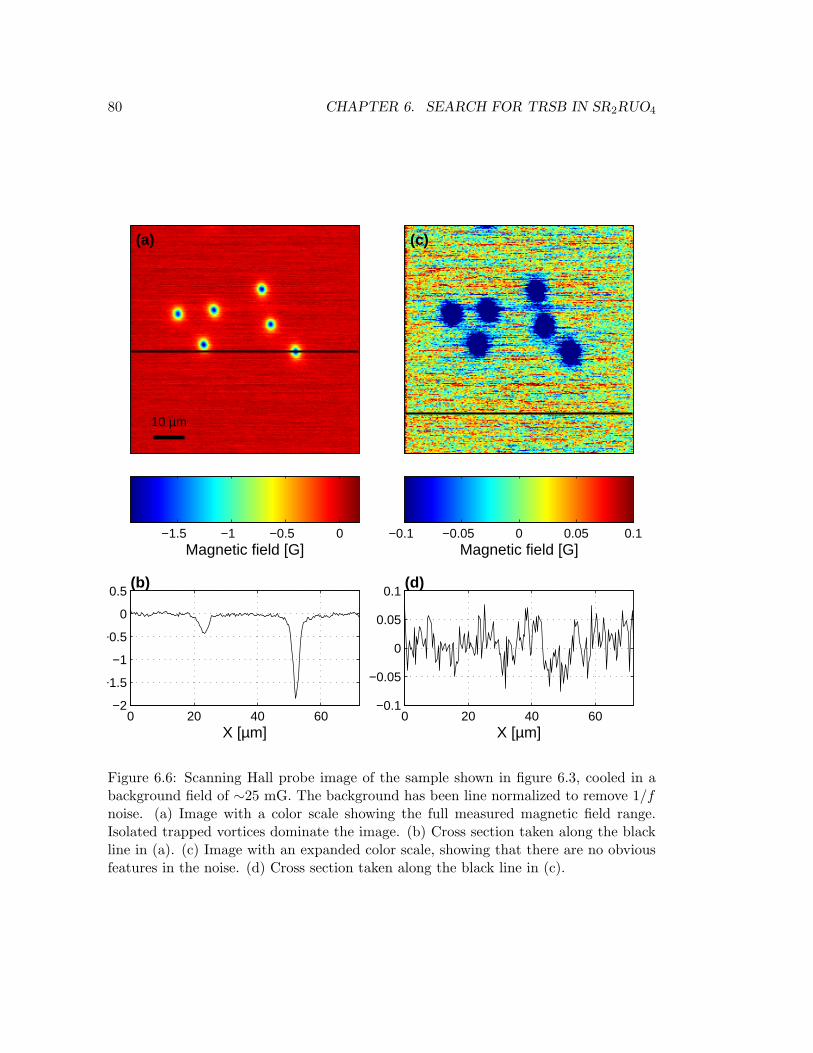
80 CHAPTER 6. SEARCH FOR TRSB IN SR2RUO4
10 µm
(a)
0 20 40 60−2
−1.5
−1
−0.5
0
0.5
X [µm]
(b)
0 20 40 60−0.1
−0.05
0
0.05
0.1
X [µm]
(d)
Magnetic field [G]−1.5 −1 −0.5 0
(c)
Magnetic field [G]−0.1 −0.05 0 0.05 0.1
Figure 6.6: Scanning Hall probe image of the sample shown in figure 6.3, cooled in abackground field of ∼25 mG. The background has been line normalized to remove 1/fnoise. (a) Image with a color scale showing the full measured magnetic field range.Isolated trapped vortices dominate the image. (b) Cross section taken along the blackline in (a). (c) Image with an expanded color scale, showing that there are no obviousfeatures in the noise. (d) Cross section taken along the black line in (c).
6.2. DETECTING TRSB USING LOCAL MAGNETIC MEASUREMENTS 81
< 25 mG
10 µm
125 mG
1 G
2 G
5 G
10 G
Mag
netic
fiel
d [G
]
0
2
4
6
8
10
Figure 6.7: Hall probe scans in varying magnetic fields. The vortices appear to formlines that are spaced much more closely than the FIB-milled hole pattern. There arealso regions at the top and right-hand side of the imaged area in which the density ofvortices is much lower than the average in the images.

82 CHAPTER 6. SEARCH FOR TRSB IN SR2RUO4
6.2.4 Hall probe data in applied background fields
Scanning Hall probe images were also made after cooling the sample through Tc in
fields up to 10 G, staying well below Hc1 (Fig. 6.7). In this field range, we would expect
to see isolated trapped vortices. The most striking feature in the images is that the
vortex distribution looks very inhomogeneous. In addition, in the densely populated
areas, the vortices appear to form lines. We have not observed (optically or using SEM)
any imperfections or structure in the crystal on length scales that correspond to these
lines, although we can not entirely rule out some kind of damage, possibly from the
FIB patterning; however, the length scale of the features does not appear to correspond
to the hole array row and column spacing. As seen in figure 6.8, the vortices appear
to be pinned in the same areas at different field levels, even though the sample was
thermally cycled above Tc between the measurements. This indicates that the vortex
pinning structure is related to some structural property of the sample, or at least some
property that is preserved across thermal cycling through Tc.
The vortex structures that we detected in the measurements in moderate fields are
similar to the structures seen by Dolocan et al. [Dolocan et al., 2004] in that the
vortices group already in small perpendicular fields. However, we find that the vortices
order in lines without any applied in-plane field (other than any residual field in the
magnetically shielded dewar or an in-plane field caused by the field inhomogeneity of
our magnet, both of which are small compared to the applied perpendicular field; the
in-plane field is estimated to be a few percent of the applied field, or a few tens of mG
in nominal zero applied field) while Dolocan et al. see the vortex pattern evolving from
irregularly shaped flux domains to a line-like structure with increasing applied in-plane
fields. In order to get a line-like structure they need to apply in-plane fields which are
much larger than the applied perpendicular field. There is a possibility that sample
differences play a significant role; they report a Tc of 1.35± 0.05 K, which is lower than
the Tc of the sample I have studied. This may be relevant, since the Tc of Sr2RuO4 is
very sensitive to sample purity [Mackenzie and Maeno, 2003].
6.3 Comparison with Theoretical Predictions
Given that we have not detected any magnetic signatures of TRSB in our scanning
measurements, it is important to compare the theoretical expectations of spontaneous

6.3. COMPARISON WITH THEORETICAL PREDICTIONS 83
1 G vortex positions overlaid on 5 G scan
10 µmM
agne
tic fi
eld
[G]
0
1
2
3
4
5
6
7
8
9
10
Figure 6.8: Overlay of the vortex positions in the 1 G scan on the 5 G scan data; thedata is the same as in Fig. 6.7. The vortex positions in the 1 G scan are marked withcircles. The vortices tend to line up in the same areas even though the sample has beenthermal cycled above TC between the measurements.

84 CHAPTER 6. SEARCH FOR TRSB IN SR2RUO4
currents with the limits set by our measurements.
One way to quantify the non-detection of edge currents is to consider the field
generated by a current loop. A circulating current around a 1 µm diameter hole would
give a measured signal of approximately 1 mG/µA at our measurement height. Thus
the measurements set a limit on net circulating currents of less than 35 µA. The total
edge current and counter-circulating shielding current could each be considerably larger.
We can also compare our non-observation of edge currents at micro-holes to the
calculation by Kwon, Yakovenko, and Sengupta for magnetic flux resulting from edge
currents [Kwon et al., 2003]. Naıvely, the predicted magnetic flux of 2.6 Gµm per unit
length of edge should fall off like the inverse of the height, leading to a magnetic field of
slightly under 1 G at a height of 1 µm. Although a self-consistent calculation including
Meissner effects in three dimensions for our specific geometry is necessary to make truly
quantitative comparisons, this naıve estimate for TRSB is well above our noise level of
35 mG.
Our non-observation of edge currents could be explained in three ways: either the
preceding estimate for TRSB edge currents is insufficient; or there are multiple chiral
domains, on the length scale of the micro-holes; or the material is not TRSB. It is
therefore important to understand the possible structure and magnetic signature of
chiral domains.
If the size of the domains is much larger than λab, the magnetic moment should be
shielded in the interior of the domains and the only measurable signal should come from
domain walls. Both the shielding currents and the neighboring domains would lead to
a cancellation of the signal when measured at a height which is large compared to ξab
and λab, but setting quantitative limits on currents at domain walls requires a specific
theoretical model.
If the size of the domains is on the order of λab or smaller, the magnetic moment
will not be fully shielded in the interior of the domain. Signals of opposite sign from
neighboring domains will cancel out rapidly with sensor height or size. The signal at a
given height from many domains can be estimated as follows. If the magnetic field at the
sample surface is Fourier transformed into its spectral components Bz(~k, z = 0), where
~k is the spatial wavevector in the plane of the sample surface, then the amplitude of
each spectral component at the height z above the surface will be decreased by a factor
of e−kz [Roth et al., 1989]. The actual measurable field would be strongly dependent on
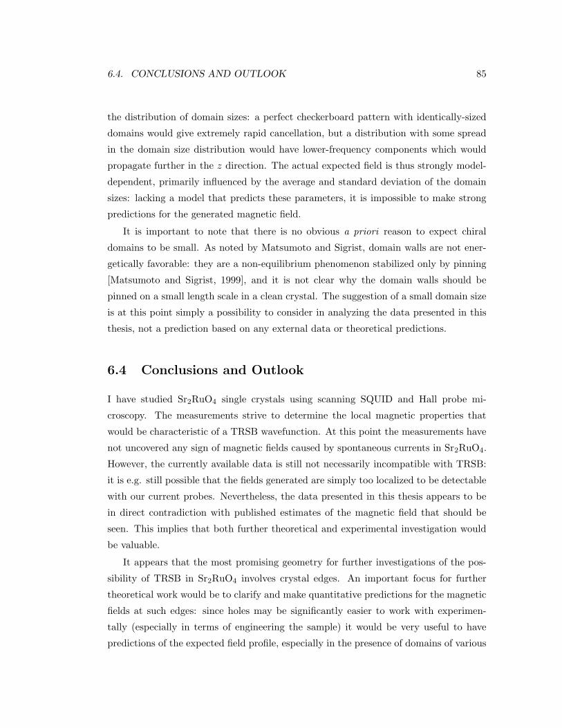
6.4. CONCLUSIONS AND OUTLOOK 85
the distribution of domain sizes: a perfect checkerboard pattern with identically-sized
domains would give extremely rapid cancellation, but a distribution with some spread
in the domain size distribution would have lower-frequency components which would
propagate further in the z direction. The actual expected field is thus strongly model-
dependent, primarily influenced by the average and standard deviation of the domain
sizes: lacking a model that predicts these parameters, it is impossible to make strong
predictions for the generated magnetic field.
It is important to note that there is no obvious a priori reason to expect chiral
domains to be small. As noted by Matsumoto and Sigrist, domain walls are not ener-
getically favorable: they are a non-equilibrium phenomenon stabilized only by pinning
[Matsumoto and Sigrist, 1999], and it is not clear why the domain walls should be
pinned on a small length scale in a clean crystal. The suggestion of a small domain size
is at this point simply a possibility to consider in analyzing the data presented in this
thesis, not a prediction based on any external data or theoretical predictions.
6.4 Conclusions and Outlook
I have studied Sr2RuO4 single crystals using scanning SQUID and Hall probe mi-
croscopy. The measurements strive to determine the local magnetic properties that
would be characteristic of a TRSB wavefunction. At this point the measurements have
not uncovered any sign of magnetic fields caused by spontaneous currents in Sr2RuO4.
However, the currently available data is still not necessarily incompatible with TRSB:
it is e.g. still possible that the fields generated are simply too localized to be detectable
with our current probes. Nevertheless, the data presented in this thesis appears to be
in direct contradiction with published estimates of the magnetic field that should be
seen. This implies that both further theoretical and experimental investigation would
be valuable.
It appears that the most promising geometry for further investigations of the pos-
sibility of TRSB in Sr2RuO4 involves crystal edges. An important focus for further
theoretical work would be to clarify and make quantitative predictions for the magnetic
fields at such edges: since holes may be significantly easier to work with experimen-
tally (especially in terms of engineering the sample) it would be very useful to have
predictions of the expected field profile, especially in the presence of domains of various

86 CHAPTER 6. SEARCH FOR TRSB IN SR2RUO4
sizes.
In terms of experimental work, there appear to be two important avenues to improve
the measurements: improving the spatial resolution and the optimizing the samples for
maximum signal and ease of modeling.
Making measurements which truly probe the magnetic fields on the length scale
set by the coherence length ξ would provide much stronger evidence on the subject of
TRSB than the current measurements, since ξ sets a lower bound on sizes of chiral
domains. This should be possible with new Hall probes with spatial resolution as fine
as 100 nm, which are currently being tested.
On the sample side, the samples I have used for the measurements reported here had
dimples as edges. It is significantly clearer and simpler to model the expected effects
of through holes or outside edges of a crystal. Of these sample geometries, through
holes are likely to be significantly easier to fabricate: a polished thin slice of crystal
can be penetrated using FIB milling. In terms of measurements, using small grains or
islands makes it more difficult to separate fringe effects of small environmental fields
from spontaneous fields from the sample. Thus it appears that high-resolution imaging
of a sample with through holes may be the best route forward to finally settle the issue
of possible TRSB in Sr2RuO4 experimentally using scanning microscopy.

Chapter 7
Local Susceptibility of The 3K
Phase of Sr2RuO4
In this chapter I discuss local SQUID susceptibility measurements on the “3 K phase”
of Sr2RuO4, which contains inclusions of metallic Ru. This is a phase of the material
in which there are signs of superconductivity already at around 3 K. This is one of
the interesting properties of Sr2RuO4 beyond the possibility of a TRSB wavefunction;
in fact at this point it is not clear if there is any relationship between the wavefunc-
tion symmetry and related properties and the apparently locally enhanced Tc in these
samples with embedded metal grains.
I will first present a brief overview of what is known about the 3 K phase, and then
continue with my observations and conclusions that can be drawn from them.
7.1 The 3 K Phase: Sr2RuO4 with Embedded Ruthenium
In certain samples of Sr2RuO4, the superconducting transition can be much broader
than in the pure samples and reach up to 3 K. Because of this property, this material
phase is often called the “3 K phase”. The nature of this phase was first reported by
Maeno et al. in 1998 [Maeno et al., 1998], and it was found to be present in samples
containing inclusions of pure metallic Ru. This commonly happens in parts of Sr2RuO4
crystals as a consequence of the growth process.
The higher Tc of the 3 K phase cannot be explained by the Ru inclusions going
superconducting since bulk Ru is superconducting only below about 0.5 K. Maeno et al.
87

88 CHAPTER 7. LOCAL SUSCEPTIBILITY OF THE 3K PHASE OF SR2RUO4
also report an anisotropy in Hc2 that is consistent with superconductivity in the layered
Sr2RuO4 structure, not in the relatively symmetric Ru grains [Maeno et al., 1998]. Mao
et al. have performed tunneling measurements and have observed signs of Andreev
bound states which they interpret as a sign of localized non-s-wave superconductivity
in the 3 K phase, which likely undergoes a phase transition close to the bulk Sr2RuO4 Tc
into a phase which is similar to the bulk superconducting phase, leading to an essentially
homogeneous superconductor below the bulk Tc [Mao et al., 2001].
7.2 Experiments
I have studied a polished sample of the 3 K phase, prepared by Karl Nelson and Ying
Liu at The Pennsylvania State University, down to temperatures well below the bulk
Ru Tc. The sample we used had been studied earlier by John Kirtley in a scanning
microscope in a 3He refrigerator at temperatures down to slightly below 300 mK.
In our setup we could only perform measurements below the bulk Sr2RuO4 Tc, using
4K measurements as zero-level reference; the temperature stability of the refrigerator
between 1.5 K and 4 K is too poor to do scanning microscopy. A series of scans at
decreasing temperature is shown in Fig. 7.2.
In the upper part of the temperature range, between approximately 500 mK and
1.5 K, we found that the sample as expected had a fairly homogeneous diamagnetic
susceptibility. Since the thickness of the Ru lamella, which appears to be on the order
of 1 µm, is much smaller than the size of the field coil of the susceptometer SQUID,
a weaker diamagnetic response from the inclusions than the bulk would likely not be
detectable; only an enhancement compared to the bulk value should give a detectable
signal. Thus, unless the superfluid density in the inclusions is higher than that of the
bulk Sr2RuO4, this signal is expected to be completely dominated by the bulk Sr2RuO4
response. This matches our susceptibility images above 500 mK very well.
At temperatures below 500 mK, a striking inhomogeneity develops in the suscep-
tibility response of the sample. The pattern of patches with enhanced diamagnetic
response are within the range expected for the density of Ru inclusions seen in the sam-
ple using optical microscopy. Since the microscope has no coarse-motion capabilities
and there is thus no way to determine the measurement area precisely, the spatially
varying density of inclusions in the sample make it impossible to determine the expected

7.2. EXPERIMENTS 89
Figure 7.1: Micrograph of the 3K phase sample studied. The Ru inclusions in the sampleare visible as bright spots. The inclusions are distributed unevenly in the sample. Weattempted to scan an area where the inclusions could be seen individually with ourscanning SQUID resolution.

90 CHAPTER 7. LOCAL SUSCEPTIBILITY OF THE 3K PHASE OF SR2RUO4
100 mK
20 µm
200 mK 300 mK 400 mK
500 mK 600 mK 700 mK 800 mK
900 mK 1000 mK
Susceptibility [Φ0/A]
−350 −300 −250
Figure 7.2: Scans of the 3K phase sample at temperatures up to 1K. The susceptibility isrelatively uniform above the bulk Ru Tc, but becomes strikingly inhomogeneous belowthat temperature.

7.3. CONCLUSIONS 91
density of Ru inclusions in the scanned region. Nevertheless, from optical micrographs
such as that shown in Fig. 7.1 typical distances between inclusions appear to be in the
10 – 30 µm range. The centers of the areas with enhanced diamagnetic susceptibility
in Fig. 7.2 generally fall within this range. Thus the most likely source of the enhanced
inhomogeneous response is that the Ru inclusions develop superconductivity separately
from the Sr2RuO4 matrix.
In order to investigate the temperature dependence of the susceptibility of the 3 K
phase sample, we measured the susceptibility while slowly adjusting the temperature
at two nearby points within the scan range, one at a response maximum and one at a
minimum point. The data is summarized in Fig. 7.3. The enhanced response turns on
at 0.47 K and the response increases smoothly in a fashion consistent with the superfluid
density increasing with decreasing temperature. The response does strengthen even at
the “low-response” point; however, this can be due to some pickup of signal from the
inclusions even in the areas between them due to the limited spatial resolution of the
SQUID probe.
7.3 Conclusions
One important conclusion of this experiment is that in order to study the intrinsic
properties of Sr2RuO4 it is very important that the samples do not contain any Ru
inclusions, since these inclusions appear to have properties that differ significantly from
the bulk. Our measurements do not provide any direct information about the symmetry
properties of the superconducting wavefunction in the inclusions; however, given that
the temperature at which the enhanced diamagnetic susceptibility is seen matches the
Tc of bulk Ru, a starting hypothesis could be that the inclusions behave just like bulk
Ru, thus exhibiting s-wave superconductivity.
The measurements presented here do not affect any conclusions about the higher-
temperature behavior of the phase; however, they do strengthen strengthen the hypoth-
esis that the superconductivity above the bulk Tc of Sr2RuO4 is an effect that is caused
by the Ru/Sr2RuO4 interface, not something that happens inside the Ru inclusions, and
that this effect may not be related to the wavefunction symmetry inside the inclusions.
In the 3 K phase, I have demonstrated that there is a significant increase in the
local diamagnetic susceptibility at temperatures below the Tc of metallic Ru. This
92 CHAPTER 7. LOCAL SUSCEPTIBILITY OF THE 3K PHASE OF SR2RUO4
0 100 200 300 400 500 600 700260
280
300
320
340
360
380
400
T [mK] (RuOx on M/C)
χ [Φ
0/A]
Susceptibility of Ru−rich Sr2RuO
4
1
2
Point 1Point 2
Figure 7.3: Temperature dependence of the local susceptibility of a 3K phase. Theblue curve corresponds to a pint with strong additional susceptibility response below0.45 K (Point 1 in the inset figure), while the green curve is the response at a nearbylow-response point (Point 2). Inset: Scan of the sample at 100 mK, where the Ruinclusions show up as areas with strong susceptibility response.

7.3. CONCLUSIONS 93
indicates that the inclusions either become superconducting at this temperature, or
that the character of the superconductivity changes locally in the material, likely in the
Ru inclusions.

94 CHAPTER 7. LOCAL SUSCEPTIBILITY OF THE 3K PHASE OF SR2RUO4

Bibliography
P. W. Anderson. Knight shift in superconductors. Phys. Rev. Lett., 3:325 – 326, 1959.
G. Binnig and H. Rohrer. Scanning tunnelling microscopy. Helvetica Physica Acta, 55
(6):726 – 735, 1982.
G. Binnig, C. F. Quate, and C. Gerber. Atomic force microscope. Phys. Rev. Lett., 56:
930 – 933, 1986.
Per G. Bjornsson, Brian W. Gardner, John R. Kirtley, and Kathryn A. Moler. Scanning
superconducting quantum interference device microscope in a dilution refrigerator.
Rev. Sci. Instr., 72:4153 – 4158, 2001.
Per G. Bjornsson, Martin E. Huber, and Kathryn A. Moler. A scanning squid micro-
scope in a dilution refrigerator. Physica B, 329 – 333:1491 – 1492, 2003.
Per G. Bjornsson, Yoshiteru Maeno, Martin E. Huber, and Kathryn A. Moler. Scanning
magnetic imaging of Sr2RuO4. Phys. Rev. B., 72:012504, 2005.
M. Buttiker, Y. Imry, and R. Landauer. Josephson behavior in small normal one-
dimensional rings. Phys. Lett., 96A:365 – 367, 1983.
B. Cabrera, R.M. Clarke, P. Colling, A.J. Miller, S. Nam, and R. W. Romani. Detection
of single infrared, optical, and ultraviolet photons using superconducting transition
edge sensors. Applied Physics Letters, 73:735 – 737, 1998.
V. Chandrasekhar, R. A. Webb, M. J. Brady, M. B. Ketchen, W. J. Gallagher, and
A. Kleinsasser. Magnetic response of a single, isolated gold loop. Phys. Rev. Lett.,
67:3578 – 3581, 1991.
95

96 BIBLIOGRAPHY
A. M. Chang, H. D. Hallen, L. Harriott, H. F. Hess, H. L. Kao, J. Kwo, R. E. Miller,
R. Wolfe, J. Vanderziel, and T. Y. Chang. Scanning Hall probe microscopy. Appl.
Phys. Lett., 61:1974 – 1976, 1992.
K. Deguchi, Z. Q. Mao, H. Yaguchi, and Y. Maeno. Gap structure of the spin-triplet
superconductor Sr2RuO4 determined from the field-orientation dependence of the
specific heat. Phys. Rev. Lett., 92:047002, 2004a.
K. Deguchi, Z.Q. Mao, and Y. Maeno. Determination of the superconducting gap
structure in all bands of the spin-triplet superconductor Sr2RuO4. Journ. Phys. Soc.
Jpn., 73:1313 – 1323, 2004b.
V. O. Dolocan, C. Veauvy, Y. Liu, F. Servant, P. Lejay, D. Mailly, and K. Hassel-
bach. Observation of vortex coalescence in the anisotropic spin-triplet superconductor
Sr2RuO4. cond-mat/0406195, 2004.
B.W. Gardner, J.C. Wynn, P.G. Bjornsson, E.W.J. Straver, J.R. Kirtley, M.B. Ketchen,
and K.A. Moler. Scanning superconducting quantum interference device susceptom-
etry. Review of Scientific Instruments, 72:2361 – 2364, 2001.
P.E. Goa, H. Hauglin, M. Baziljevich, E. Il’yashenko, P. L. Gammel, and T. H. Jo-
hansen. Real-time magneto-optical imaging of vortices in superconducting NbSe2.
Superconductor Science & Technology, 14:729 – 731, 2001.
Janice Wynn Guikema. Scanning Hall Probe Microscopy of Magnetic Vortices in Very
Underdoped Yttrium-Barium-Copper-Oxide. PhD thesis, Stanford university, 2004.
Hans-Ulrich Habermeier. Paing the way for the success of magneto-optics. In Tom H.
Johansen and Daniel V. Shantsev, editors, Magneto-Optical Imaging, NATO Science
Series, pages 1 – 10. Kluwer Academic Publishers, 2004.
K. Hasselbach, C. Veauvy, and D. Mailly. MicroSQUID magnetometry and magnetic
imaging. Physica C, 332:140 –147, 2000.
Martin E. Huber, Bethel G. Abraham, Leonard J. Archuleta, Tommy Azua, Anthony J.
Caravella, Son Duong, Sean T. Halloran, Erik A. Lucero, James T. B. Snodgrass,
Per G. Bjornsson, Brian W. Gardner, and Kathryn A. Moler. Well-shielded, high-
symmetery scanning squid susceptometer. (in preparation.).

BIBLIOGRAPHY 97
Martin E. Huber, Patricia A. Neil, Robert G. Benson, Deborah A. Burns, Alan M.
Corey, Christopher S . Flynn, Yevgeniya Kitaygorodskaya, Omid Massihzadeh,
John M. Martinis, and G. C. I-Iilton. DC SQUID series array amplifiers with 120
MHz bandwidth. IEEE Trans. Appl. Supercond., 11:1251 – 1256, 2001.
Hypres, Inc. Design rules, As available online in June 2005. URL
http://www.hypres.com/pages/download/designrules/rules.pdf.
K. Ishida, H. Mukuda, Y. Kitaoka, K. Asayama, Z. Q. Mao, Y. Mori, and Y. Maeno.
Spin-triplet superconductivity in Sr2RuO4 identified by O-17 knight shift. Nature,
396:658 – 660, 1998.
K. Izawa, H. Takahashi, H. Yamaguchi, Yuji Matsuda, M. Suzuki, T. Sasaki, T. Fukase,
Y. Yoshida, R. Settai, and Y. Onuki. Superconducting gap structure of spin-triplet
superconductor Sr2RuO4 studied by thermal conductivity. Phys. Rev. Lett., 86(12):
2653 – 2656, 2001.
John David Jackson. Classical Electrodynamics. John Wiley and Sons, Inc., third
edition edition, 1999.
E. M. Q. Jariwala, P. Mohanty, M. B. Ketchen, and R. A. Webb. Diamagnetic persistent
current in diffusive normal-metal rings. Phys. Rev. Lett., 86:1594 – 1597, 2001.
Mark Johnson and John Clarke. Spin-polarized scanning tunneling microscope: Con-
cept, design and preliminary results from a prototype operated in air. J. Appl. Phys.,
67:6141 – 6152, 1990.
B. D. Josephson. Possible new effects in superconductive tunneling. Phys. Lett., 1:251
– 253, 1962.
P. G. Kealey, T. M. Riseman, E. M. Forgan, L. M. Galvin, A. P. Mackenzie, S. L.
Lee, D. M. Paul, R. Cubitt, D. F. Agterberg, R. Heeb, Z. Q. Mao, and Y. Maeno.
Reconstruction from small-angle neutron scattering measurements of the real space
magnetic field distribution in the mixed state of Sr2RuO4. Phys. Rev. Lett., 84(26):
6094 – 6097, 2000.
M. B. Ketchen and J. R. Kirtley. Design and performance aspects of pickup loop

98 BIBLIOGRAPHY
structures for miniature squid magnetometry. IEEE Trans. Appl. Supercond., 5:2133
– 2136, 1995.
M. B. Ketchen, D. D. Awschalom, W. J. Gallagher, A. W. Kleinsasser, R. L. Sandstrom,
J. R. Rosen, and B. Bumble. Design, fabrication, and performance of integrated
miniature squid susceptometers. IEEE Trans. Mag., 25:1212 – 1215, 1989.
M. B. Ketchen, M. Bushan, S. B. Kaplan, and W. J. Gallagher. Low-noise dc SQUIDs
fabricated in Nb-Al2O3-Nb trilayer technology. IEEE Trans. Mag., 27:3005, 1991.
Mark B. Ketchen, T. Kopley, and H. Ling. Miniature squid susceptometer. Appl. Phys.
Lett., 44:1008, 1984.
J. R. Kirtley, M. B. Ketchen, C. C. Tsuei, J. Z. Sun, W. J. Gallagher, Lock See Yu-
Jahnes, A. Gupta, and K. G. Stawiaszand S. J. Wind. Design and applications of
a scanning squid microscope. IBM Journal of Research and Development, 39:655 –
668, 1995.
J. R. Kirtley, V. G. Kogan, J. R. Clem, and K. A. Moler. Magnetic field of an in-plane
vortex outside a layered superconductor. Phys. Rev. B, 59:4343 – 4348, 1999.
H. J. Kwon, V. M. Yakovenko, and K. Sengupta. How to detect edge electron states in
(tmtsf)(2)x and Sr2RuO4 experimentally. Synthetic Metals, 133:27 – 31, 2003.
L. P. Levy, G. Dolan, J. Dunsmuir, and H. Bouchiat. Magnetization of copper rings:
Evidence for persistent currents. Phys. Rev. Lett., 64:2074 – 2077, 1990.
G. M. Luke, Y. Fudamoto, K. M. Kojima, M. I. Larkin, J. Merrin, B. Nachumi, Y. J.
Uemura, Y. Maeno, Z. Q. Mao, Y. Mori, H. Nakamura, and M. Sigrist. Time-reversal
symmetry-breaking superconductivity in Sr2RuO4. Nature, 394:558 – 561, 1998.
A. P. Mackenzie and Y. Maeno. The superconductivity of Sr2RuO4 and the physics of
spin-triplet pairing. Rev. Mod. Phys., 75:657, 2003.
Y. Maeno, H. Hashimoto, K. Yoshida, S. Nishizaki, T. Fujita, J. G. Bednorz, and
F. Lichtenberg. Superconductivity in a layered perovskite without copper. Nature,
372:532 – 534, 1994.
BIBLIOGRAPHY 99
Y. Maeno, T. Ando, Y. Mori, E. Ohmichi, S. Ikeda, S. NishiZaki, and S. Nakatsuji.
Enhancement of superconductivity of Sr2RuO4 to 3 k by embedded metallic mi-
crodomains. Phys. Rev. Lett., 81:3765 – 3768, 1998.
D. Mailly, C. Chapelier, and A. Benoit. Experimental observation of persistent currents
in a gaas-algaas single loop. Phys. Rev. Lett., 70:2020 – 2023, 1993.
Z. Q. Mao, Y. Maeno, and H. Fukazawa. Crystal growth of Sr2RuO4. Mater. Res. Bull.,
35:1813, 2000.
Z. Q. Mao, K. D. Nelson, R. Jin, and Y. Liu. Observation of andreev surface bound
states in the 3-k phase region of Sr2RuO4. Phys. Rev. Lett., 87:037003, 2001.
Masashige Matsumoto and Manfred Sigrist. Quasiparticle states near the surface and
the domain wall in a px ± ipy-wave superconductor. Jornal of the Physical Society of
Japan, 68:994 – 1007, 1999.
K. D. Nelson, Z. Q. Mao, Y. Maeno, and Y. Liu. Odd-parity superconductivity in
Sr2RuO4. Science, 306:1151 – 1154, 2004.
S. Nishizaki, Y. Maeno, and Z. Q. Mao. Effect of impurities on the specific heat of the
spin-triplet superconductor Sr2RuO4. J. Low Temp. Phys., 117:1581, 1999.
R. J. Noer and W. D. Knight. Nuclear magnetic resonance and relaxation in supercon-
ducting vanadium. Rev. Mod. Phys., 36:177 – 185, 1964.
A. Oral, S. J. Bending, and M M. Henini. Real-time scanning Hall probe microscopy.
Appl. Phys. Lett., 69:1324 – 1326, 1996.
Bradley J. Roth, Nestor G. Sepulveda, and Jr. John P. Wickswo. Using a magnetometer
to image a two-dimensional current distribution. J. Appl. Phys., 65:361 – 372, 1989.
A. L. Schawlow. Structure of the intermediate state in superconductors. Phys. Rev.,
101:573 – 579, 1956.
J. Siegel, J. Witt, N. Venturi, and S. Field. Compact large-range cryogenic scanner.
Rev. Sci. Instr., 66:2520 – 2523, 1995.
Manfred Sigrist and Kazuo Ueda. Phenomenological theory of unconventional super-
conductivity. Reviews of Modern Physics, 63:239 – 308, 1991.
100 BIBLIOGRAPHY
T. D. Stowe, K. Yasumura, T. W. Kenny, D. Botkin, K. Wago, and D. Rugar. At-
tonewton force detection using ultrathin silicon cantilevers. Appl. Phys. Lett., 71:288
– 290, 1997.
Eric W J Straver. Cantilever-based measurements on nanomagnets and superconductors.
PhD thesis, Stanford University, 2004.
T. Tamegai, K. Yamazaki, M. Tokunaga, Z. Mao, and Y. Maeno. Search for spontaneous
magnetization in Sr2RuO4. Physica C, 388 – 389:499 – 500, 2003.
M. A. Tanatar, S. Nagai, Z. Q. Mao, Y. Maeno, and T. Ishiguro. Thermal conductivity
of superconducting Sr2RuO4 in oriented magnetic fields. Phys. Rev. B, 63:064505,
2001a.
M. A. Tanatar, M. Suzuki, S. Nagai, Z. Q. Mao, Y. Maeno, and T. Ishiguro. Anisotropy
of magnetothermal conductivity in Sr2RuO4. Phys. Rev. Lett., 86(12):2649 – 2652,
2001b.
C. D. Tesche and J. Clarke. DC SQUID: noise and optimization. Journal of Low
Temperature Physics, 29:301 – 331, 1977.
Michael Tinkham. Introduction to Superconductivity. McGraw-Hill, 2 edition, 1996.
A. Tonomura, H. Kasai, O. Kamimura, T. Matsuda, K. Harada, Y. Nakayama, J. Shi-
moyama, K. Kishio, T. Hanaguri, K. Kitazawa, M. Sasasek, and S. Okayasuk. Ob-
servation of individual vortices trapped along columnar defects in high-temperature
superconductors. Nature, 412:620 – 622, 2001.
Akira Tonomura. Electron phase microscopy and its applications to the observation of
vortex dynamics. Jpn. J. Appl. Phys., 34:2951 – 2964, 1995.
M. J. Uren, D. J. Day, and M. J. Kirton. 1/f and random telegraph noise in silicon
metal-oxide-semiconductor field-effect transistors. Appl. Phys. Lett., 47:1195 – 1197,
1985.
Theodore Van Duzer and Charles W. Turner. Principles of Superconductive Devices
and Circuits. Prentice Hall, 2 edition, 1998.
R. P. Welty and J. M. Martinis. A series array of dc squids. IEEE Trans. Mag., 27:
2924 – 2926, 1991.


