LT1965 Series
11965fb
For more information www.linear.com/LT1965
Features
applications
Description
1.1A, Low Noise,Low Dropout Linear Regulator
The LT®1965 series are low noise, low dropout linear regu-lators. The devices supply 1.1A of output current with a 310mV typical dropout voltage. Operating quiescent current is 500µA for the adjustable version, reducing to <1µA in shutdown. Quiescent current is well controlled; it does not rise in dropout as with many other regulators. The LT1965 regulators have very low output noise which makes them ideal for sensitive RF and DSP supply applications.
Output voltage ranges from 1.20V to 19.5V. The LT1965 regulators are stable with output capacitors as low as 10µF. Internal protection circuitry includes reverse-battery protection, current limiting with foldback, thermal limit-ing and reverse-current protection. The LT1965 series are available in fixed output voltages of 1.5V, 1.8V, 2.5V, 3.3V, and as an adjustable device with a 1.20V reference voltage. The package offerings include the 5-lead TO-220, 5-lead DD-Pak as well as the thermally enhanced 8-lead MSOP and low profile (0.75mm) 8-lead 3mm × 3mm DFN.
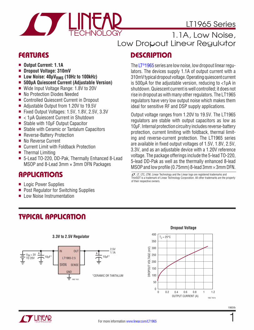
3.3V to 2.5V Regulator
n Output Current: 1.1An Dropout Voltage: 310mVn Low Noise: 40µVRMS (10Hz to 100kHz)n 500µA Quiescent Current (Adjustable Version)n Wide Input Voltage Range: 1.8V to 20Vn No Protection Diodes Neededn Controlled Quiescent Current in Dropoutn Adjustable Output from 1.20V to 19.5Vn Fixed Output Voltages: 1.5V, 1.8V, 2.5V, 3.3Vn < 1µA Quiescent Current in Shutdownn Stable with 10µF Output Capacitorn Stable with Ceramic or Tantalum Capacitorsn Reverse-Battery Protectionn No Reverse Currentn Current Limit with Foldback Protectionn Thermal Limitingn 5-Lead TO-220, DD-Pak, Thermally Enhanced 8-Lead
MSOP and 8-Lead 3mm × 3mm DFN Packages
n Logic Power Suppliesn Post Regulator for Switching Suppliesn Low Noise Instrumentation
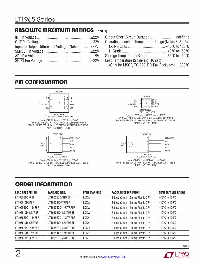
Dropout Voltage
typical application
OUTPUT CURRENT (A)0
0
DROP
OUT
VOLT
AGE
(mV)
100
200
300
0.2 0.4 0.6 0.8 1
400
50
150
250
350
1.2
1965 TA01b
TJ = 25°C
IN
SHDN
10µF*
*CERAMIC OR TANTALUM1965 TA01
OUTVIN > 3VTO 20V
SENSE
GND
LT1965-2.5
2.5V1.1A
10µF*++
L, LT, LTC, LTM, Linear Technology and the Linear logo are registered trademarks and ThinSOT is a trademark of Linear Technology Corporation. All other trademarks are the property of their respective owners.
LT1965 Series
21965fb
For more information www.linear.com/LT1965
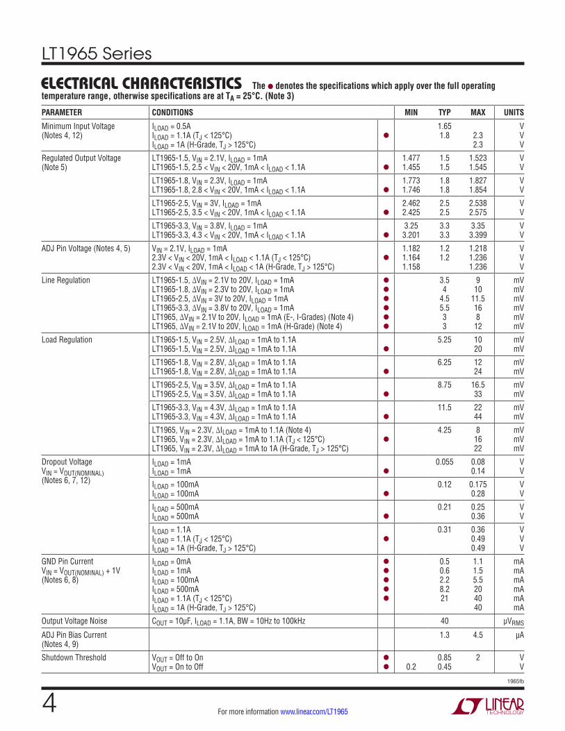
absolute MaxiMuM ratingsIN Pin Voltage .........................................................±22VOUT Pin Voltage ......................................................±22VInput to Output Differential Voltage (Note 2) ......... ±22VSENSE Pin Voltage ..................................................±22VADJ Pin Voltage ........................................................±9VSHDN Pin Voltage ...................................................±22V
(Note 1)
TOP VIEW
DD PACKAGE8-LEAD (3mm × 3mm) PLASTIC DFN
5
6
7
8
9
4
3
2
1OUT
OUT
SENSE/ADJ*
GND
IN
IN
SHDN
GND
TJMAX = 150°C, θJA = 65°C/W, θJC = 3°C/W
EXPOSED PAD (PIN 9) IS GND, MUST BE SOLDERED TO PCB *PIN 3 = SENSE FOR LT1965-1.5/LT1965-1.8/LT1965-2.5/LT1965-3.3
*PIN 3 = ADJ FOR LT1965
1234
OUTOUT
SENSE/ADJ*GND
8765
9
ININSHDNGND
TOP VIEW
MS8E PACKAGE8-LEAD PLASTIC MSOP
TJMAX = 125°C, θJA = 60°C/W, θJC = 10°C/WEXPOSED PAD (PIN 9) IS GND, MUST BE SOLDERED TO PCB
*PIN 3 = SENSE FOR LT1965-1.5/LT1965-1.8/LT1965-2.5/LT1965-3.3 *PIN 3 = ADJ FOR LT1965
Q PACKAGE5-LEAD PLASTIC DD-PAK
FRONT VIEW
SENSE/ADJ*
OUT
GND
IN
SHDN
TAB ISGND
5
4
3
2
1
TJMAX = 150°C, θJA = 30°C/W, θJC = 3°C/W
*PIN 5 = SENSE FOR LT1965-1.5/LT1965-1.8/LT1965-2.5/LT1965-3.3 *PIN 5 = ADJ FOR LT1965
T PACKAGE5-LEAD PLASTIC TO-220
SENSE/ADJ*
OUT
GND
IN
SHDN
FRONT VIEW
5
4
3
2
1
TAB ISGND
TJMAX = 150°C, θJA = 50°C/W, θJC = 3°C/W
*PIN 5 = SENSE FOR LT1965-1.5/LT1965-1.8/LT1965-2.5/LT1965-3.3 *PIN 5 = ADJ FOR LT1965
Output Short-Circuit Duration .......................... IndefiniteOperating Junction Temperature Range (Notes 3, 5, 13)
E-, I-Grades ....................................... –40°C to 125°C H-Grade ............................................. –40°C to 150°C
Storage Temperature Range .................. –65°C to 150°C Lead Temperature (Soldering, 10 sec) (Only for MSOP, TO-220, DD-Pak Packages) .... 300°C
LEAD FREE FINISH TAPE AND REEL PART MARKING* PACKAGE DESCRIPTION TEMPERATURE RANGE
LT1965EDD#PBF LT1965EDD#TRPBF LCXW 8-Lead (3mm × 3mm) Plastic DFN –40°C to 125°C
LT1965IDD#PBF LT1965IDD#TRPBF LCXW 8-Lead (3mm × 3mm) Plastic DFN –40°C to 125°C
LT1965EDD-1.5#PBF LT1965EDD-1.5#TRPBF LDKW 8-Lead (3mm × 3mm) Plastic DFN –40°C to 125°C
LT1965IDD-1.5#PBF LT1965IDD-1.5#TRPBF LDKW 8-Lead (3mm × 3mm) Plastic DFN –40°C to 125°C
LT1965EDD-1.8#PBF LT1965EDD-1.8#TRPBF LDKY 8-Lead (3mm × 3mm) Plastic DFN –40°C to 125°C
LT1965IDD-1.8#PBF LT1965IDD-1.8#TRPBF LDKY 8-Lead (3mm × 3mm) Plastic DFN –40°C to 125°C
LT1965EDD-2.5#PBF LT1965EDD-2.5#TRPBF LDMB 8-Lead (3mm × 3mm) Plastic DFN –40°C to 125°C
LT1965IDD-2.5#PBF LT1965IDD-2.5#TRPBF LDMB 8-Lead (3mm × 3mm) Plastic DFN –40°C to 125°C
LT1965EDD-3.3#PBF LT1965EDD-3.3#TRPBF LDMD 8-Lead (3mm × 3mm) Plastic DFN –40°C to 125°C
pin conFiguration
orDer inForMation
LT1965 Series
31965fb
For more information www.linear.com/LT1965
orDer inForMationLEAD FREE FINISH TAPE AND REEL PART MARKING* PACKAGE DESCRIPTION TEMPERATURE RANGE
LT1965IDD-3.3#PBF LT1965IDD-3.3#TRPBF LDMD 8-Lead (3mm × 3mm) Plastic DFN –40°C to 125°C
LT1965EMS8E#PBF LT1965EMS8E#TRPBF LTCXX 8-Lead Plastic MSOP –40°C to 125°C
LT1965IMS8E#PBF LT1965IMS8E#TRPBF LTCXX 8-Lead Plastic MSOP –40°C to 125°C
LT1965EMS8E-1.5#PBF LT1965EMS8E-1.5#TRPBF LTDKX 8-Lead Plastic MSOP –40°C to 125°C
LT1965IMS8E-1.5#PBF LT1965IMS8E-1.5#TRPBF LTDKX 8-Lead Plastic MSOP –40°C to 125°C
LT1965EMS8E-1.8#PBF LT1965EMS8E-1.8#TRPBF LTDKZ 8-Lead Plastic MSOP –40°C to 125°C
LT1965IMS8E-1.8#PBF LT1965IMS8E-1.8#TRPBF LTDKZ 8-Lead Plastic MSOP –40°C to 125°C
LT1965EMS8E-2.5#PBF LT1965EMS8E-2.5#TRPBF LTDMC 8-Lead Plastic MSOP –40°C to 125°C
LT1965IMS8E-2.5#PBF LT1965IMS8E-2.5#TRPBF LTDMC 8-Lead Plastic MSOP –40°C to 125°C
LT1965EMS8E-3.3#PBF LT1965EMS8E-3.3#TRPBF LTDMF 8-Lead Plastic MSOP –40°C to 125°C
LT1965IMS8E-3.3#PBF LT1965IMS8E-3.3#TRPBF LTDMF 8-Lead Plastic MSOP –40°C to 125°C
LT1965EQ#PBF LT1965EQ#TRPBF LT1965Q 5-Lead Plastic DD-Pak –40°C to 125°C
LT1965IQ#PBF LT1965IQ#TRPBF LT1965Q 5-Lead Plastic DD-Pak –40°C to 125°C
LT1965HQ#PBF LT1965HQ#TRPBF LT1965Q 5-Lead Plastic DD-Pak –40°C to 150°C
LT1965EQ-1.5#PBF LT1965EQ-1.5#TRPBF LT1965Q-1.5 5-Lead Plastic DD-Pak –40°C to 125°C
LT1965IQ-1.5#PBF LT1965IQ-1.5#TRPBF LT1965Q-1.5 5-Lead Plastic DD-Pak –40°C to 125°C
LT1965EQ-1.8#PBF LT1965EQ-1.8#TRPBF LT1965Q-1.8 5-Lead Plastic DD-Pak –40°C to 125°C
LT1965IQ-1.8#PBF LT1965IQ-1.8#TRPBF LT1965Q-1.8 5-Lead Plastic DD-Pak –40°C to 125°C
LT1965EQ-2.5#PBF LT1965EQ-2.5#TRPBF LT1965Q-2.5 5-Lead Plastic DD-Pak –40°C to 125°C
LT1965IQ-2.5#PBF LT1965IQ-2.5#TRPBF LT1965Q-2.5 5-Lead Plastic DD-Pak –40°C to 125°C
LT1965EQ-3.3#PBF LT1965EQ-3.3#TRPBF LT1965Q-3.3 5-Lead Plastic DD-Pak –40°C to 125°C
LT1965IQ-3.3#PBF LT1965IQ-3.3#TRPBF LT1965Q-3.3 5-Lead Plastic DD-Pak –40°C to 125°C
LT1965ET#PBF N/A LT1965T 5-Lead Plastic TO-220 –40°C to 125°C
LT1965IT#PBF N/A LT1965T 5-Lead Plastic TO-220 –40°C to 125°C
LT1965HT#PBF N/A LT1965T 5-Lead Plastic TO-220 –40°C to 150°C
LT1965ET-1.5#PBF N/A LT1965T-1.5 5-Lead Plastic TO-220 –40°C to 125°C
LT1965IT-1.5#PBF N/A LT1965T-1.5 5-Lead Plastic TO-220 –40°C to 125°C
LT1965ET-1.8#PBF N/A LT1965T-1.8 5-Lead Plastic TO-220 –40°C to 125°C
LT1965IT-1.8#PBF N/A LT1965T-1.8 5-Lead Plastic TO-220 –40°C to 125°C
LT1965ET-2.5#PBF N/A LT1965T-2.5 5-Lead Plastic TO-220 –40°C to 125°C
LT1965IT-2.5#PBF N/A LT1965T-2.5 5-Lead Plastic TO-220 –40°C to 125°C
LT1965ET-3.3#PBF N/A LT1965T-3.3 5-Lead Plastic TO-220 –40°C to 125°C
LT1965IT-3.3#PBF N/A LT1965T-3.3 5-Lead Plastic TO-220 –40°C to 125°C
Consult LTC Marketing for parts specified with wider operating temperature ranges. *Temperature grades are identified by a label on the shipping container. Consult LTC Marketing for information on nonstandard lead based finish parts.For more information on lead free part marking, go to: http://www.linear.com/leadfree/ For more information on tape and reel specifications, go to: http://www.linear.com/tapeandreel/
LT1965 Series
41965fb
For more information www.linear.com/LT1965
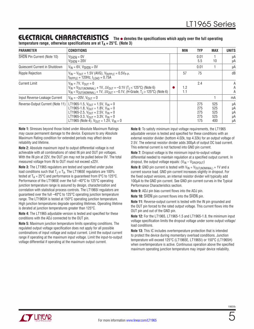
electrical characteristics
PARAMETER CONDITIONS MIN TYP MAX UNITS
Minimum Input Voltage (Notes 4, 12)
ILOAD = 0.5A ILOAD = 1.1A (TJ < 125°C) ILOAD = 1A (H-Grade, TJ > 125°C)
l
1.65 1.8
2.3 2.3
V V V
Regulated Output Voltage (Note 5)
LT1965-1.5, VIN = 2.1V, ILOAD = 1mA LT1965-1.5, 2.5 < VIN < 20V, 1mA < ILOAD < 1.1A
l
1.477 1.455
1.5 1.5
1.523 1.545
V V
LT1965-1.8, VIN = 2.3V, ILOAD = 1mA LT1965-1.8, 2.8 < VIN < 20V, 1mA < ILOAD < 1.1A
l
1.773 1.746
1.8 1.8
1.827 1.854
V V
LT1965-2.5, VIN = 3V, ILOAD = 1mA LT1965-2.5, 3.5 < VIN < 20V, 1mA < ILOAD < 1.1A
l
2.462 2.425
2.5 2.5
2.538 2.575
V V
LT1965-3.3, VIN = 3.8V, ILOAD = 1mA LT1965-3.3, 4.3 < VIN < 20V, 1mA < ILOAD < 1.1A
l
3.25 3.201
3.3 3.3
3.35 3.399
V V
ADJ Pin Voltage (Notes 4, 5) VIN = 2.1V, ILOAD = 1mA 2.3V < VIN < 20V, 1mA < ILOAD < 1.1A (TJ < 125°C) 2.3V < VIN < 20V, 1mA < ILOAD < 1A (H-Grade, TJ > 125°C)
l
1.182 1.164 1.158
1.2 1.2
1.218 1.236 1.236
V V V
Line Regulation LT1965-1.5, ∆VIN = 2.1V to 20V, ILOAD = 1mA LT1965-1.8, ∆VIN = 2.3V to 20V, ILOAD = 1mA LT1965-2.5, ∆VIN = 3V to 20V, ILOAD = 1mA LT1965-3.3, ∆VIN = 3.8V to 20V, ILOAD = 1mA LT1965, ∆VIN = 2.1V to 20V, ILOAD = 1mA (E-, I-Grades) (Note 4) LT1965, ∆VIN = 2.1V to 20V, ILOAD = 1mA (H-Grade) (Note 4)
l
l
l
l
l
l
3.5 4
4.5 5.5 3 3
9 10
11.5 16 8
12
mV mV mV mV mV mV
Load Regulation LT1965-1.5, VIN = 2.5V, ∆ILOAD = 1mA to 1.1A LT1965-1.5, VIN = 2.5V, ∆ILOAD = 1mA to 1.1A
l
5.25 10 20
mV mV
LT1965-1.8, VIN = 2.8V, ∆ILOAD = 1mA to 1.1A LT1965-1.8, VIN = 2.8V, ∆ILOAD = 1mA to 1.1A
l
6.25 12 24
mV mV
LT1965-2.5, VIN = 3.5V, ∆ILOAD = 1mA to 1.1A LT1965-2.5, VIN = 3.5V, ∆ILOAD = 1mA to 1.1A
l
8.75 16.5 33
mV mV
LT1965-3.3, VIN = 4.3V, ∆ILOAD = 1mA to 1.1A LT1965-3.3, VIN = 4.3V, ∆ILOAD = 1mA to 1.1A
l
11.5 22 44
mV mV
LT1965, VIN = 2.3V, ∆ILOAD = 1mA to 1.1A (Note 4) LT1965, VIN = 2.3V, ∆ILOAD = 1mA to 1.1A (TJ < 125°C) LT1965, VIN = 2.3V, ∆ILOAD = 1mA to 1A (H-Grade, TJ > 125°C)
l
4.25 8 16 22
mV mV mV
Dropout Voltage VIN = VOUT(NOMINAL) (Notes 6, 7, 12)
ILOAD = 1mA ILOAD = 1mA
l
0.055 0.08 0.14
V V
ILOAD = 100mA ILOAD = 100mA
l
0.12 0.175 0.28
V V
ILOAD = 500mA ILOAD = 500mA
l
0.21 0.25 0.36
V V
ILOAD = 1.1A ILOAD = 1.1A (TJ < 125°C) ILOAD = 1A (H-Grade, TJ > 125°C)
l
0.31 0.36 0.49 0.49
V V V
GND Pin Current VIN = VOUT(NOMINAL) + 1V (Notes 6, 8)
ILOAD = 0mA ILOAD = 1mA ILOAD = 100mA ILOAD = 500mA ILOAD = 1.1A (TJ < 125°C) ILOAD = 1A (H-Grade, TJ > 125°C)
l
l
l
l
l
0.5 0.6 2.2 8.2 21
1.1 1.5 5.5 20 40 40
mA mA mA mA mA mA
Output Voltage Noise COUT = 10µF, ILOAD = 1.1A, BW = 10Hz to 100kHz 40 µVRMS
ADJ Pin Bias Current (Notes 4, 9)
1.3 4.5 µA
Shutdown Threshold VOUT = Off to On VOUT = On to Off
l
l
0.2
0.85 0.45
2 V V
The l denotes the specifications which apply over the full operating temperature range, otherwise specifications are at TA = 25°C. (Note 3)
LT1965 Series
51965fb
For more information www.linear.com/LT1965
electrical characteristics
Note 1: Stresses beyond those listed under Absolute Maximum Ratings may cause permanent damage to the device. Exposure to any Absolute Maximum Rating condition for extended periods may affect device reliability and lifetime.Note 2: Absolute maximum input to output differential voltage is not achievable with all combinations of rated IN pin and OUT pin voltages. With the IN pin at 22V, the OUT pin may not be pulled below 0V. The total measured voltage from IN to OUT must not exceed ±22V.Note 3: The LT1965 regulators are tested and specified under pulse load conditions such that TJ @ TA. The LT1965E regulators are 100% tested at TA = 25°C and performance is guaranteed from 0°C to 125°C. Performance of the LT1965E over the full –40°C to 125°C operating junction temperature range is assured by design, characterization and correlation with statistical process controls. The LT1965I regulators are guaranteed over the full –40°C to 125°C operating junction temperature range. The LT1965H is tested at 150°C operating junction temperature. High junction temperatures degrade operating lifetimes. Operating lifetime is derated at junction temperatures greater than 125°C.Note 4: The LT1965 adjustable version is tested and specified for these conditions with the ADJ connected to the OUT pin. Note 5: Maximum junction temperature limits operating conditions. The regulated output voltage specification does not apply for all possible combinations of input voltage and output current. Limit the output current range if operating at the maximum input voltage. Limit the input-to-output voltage differential if operating at the maximum output current.
Note 6: To satisfy minimum input voltage requirements, the LT1965 adjustable version is tested and specified for these conditions with an external resistor divider (bottom 4.02k, top 4.32k) for an output voltage of 2.5V. The external resistor divider adds 300µA of output DC load current. This external current is not factored into GND pin current.Note 7: Dropout voltage is the minimum input-to-output voltage differential needed to maintain regulation at a specified output current. In dropout, the output voltage equals: (VIN – VDROPOUT)Note 8: GND pin current is tested with VIN = VOUT(NOMINAL) + 1V and a current source load. GND pin current increases slightly in dropout. For the fixed output versions, an internal resistor divider will typically add 100µA to the GND pin current. See GND pin current curves in the Typical Performance Characteristics section.Note 9: ADJ pin bias current flows into the ADJ pin.Note 10: SHDN pin current flows into the SHDN pin.Note 11: Reverse-output current is tested with the IN pin grounded and the OUT pin forced to the rated output voltage. This current flows into the OUT pin and out of the GND pin.Note 12: For the LT1965, LT1965-1.5 and LT1965-1.8, the minimum input voltage specification limits the dropout voltage under some output voltage/load conditions.Note 13: This IC includes overtemperature protection that is intended to protect the device during momentary overload conditions. Junction temperature will exceed 125°C (LT1965E, LT1965I) or 150°C (LT1965H)when overtemperature is active. Continuous operation above the specified maximum operating junction temperature may impair device reliability.
PARAMETER CONDITIONS MIN TYP MAX UNITS
SHDN Pin Current (Note 10) VSHDN = 0V VSHDN = 20V
0.01 5.5
1 10
µA µA
Quiescent Current in Shutdown VIN = 6V, VSHDN = 0V 0.01 1 µA
Ripple Rejection VIN – VOUT = 1.5V (AVG), VRIPPLE = 0.5VP-P, fRIPPLE = 120Hz, ILOAD = 0.75A
57 75 dB
Current Limit VIN = 7V, VOUT = 0 VIN = VOUT(NOMINAL) + 1V, ∆VOUT = –0.1V (TJ < 125°C) (Note 6) VIN = VOUT(NOMINAL) + 1V, ∆VOUT = –0.1V, (H-Grade, TJ > 125°C) (Note 6)
l
1.2 1.1
2.4 A A A
Input Reverse-Leakage Current VIN = –20V, VOUT = 0 1 mA
Reverse-Output Current (Note 11) LT1965-1.5, VOUT = 1.5V, VIN = 0 LT1965-1.8, VOUT = 1.8V, VIN = 0 LT1965-2.5, VOUT = 2.5V, VIN = 0 LT1965-3.3, VOUT = 3.3V, VIN = 0 LT1965 (Note 4), VOUT = 1.2V, VIN = 0
275 275 275 275 175
525 525 525 525 400
µA µA µA µA µA
The l denotes the specifications which apply over the full operating temperature range, otherwise specifications are at TA = 25°C. (Note 3)
LT1965 Series
61965fb
For more information www.linear.com/LT1965
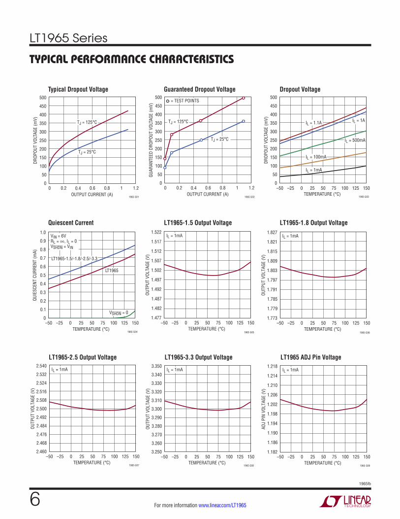
LT1965-2.5 Output Voltage LT1965-3.3 Output Voltage LT1965 ADJ Pin Voltage
typical perForMance characteristics
Typical Dropout Voltage Guaranteed Dropout Voltage Dropout Voltage
Quiescent Current LT1965-1.5 Output Voltage LT1965-1.8 Output Voltage
OUTPUT CURRENT (A)0
0
DROP
OUT
VOLT
AGE
(mV)
100
200
300
0.2 0.4 0.6 0.8 1
400
500
50
150
250
350
450
1.2
1965 G01
TJ = 125°C
TJ = 25°C
OUTPUT CURRENT (A)0
0
GUAR
ANTE
ED D
ROPO
UT V
OLTA
GE (m
V)
100
200
300
0.2 0.4 0.6 0.8 1
400
500
50
150
250
350
450
1.2
1965 G02
= TEST POINTS
TJ = 125°C
TJ = 25°C
–50 –25 0 25 50 75 125100 1500
DROP
OUT
VOLT
AGE
(mV)
100
200
300
400
500
50
150
250
350
450
1965 G03
IL = 1.1A
IL = 500mA
IL = 100mA
IL = 1mA
TEMPERATURE (°C)
IL = 1A
0
QUIE
SCEN
T CU
RREN
T (m
A)
0.2
0.4
0.6
0.8
1.0
0.1
0.3
0.5
0.7
0.9
1965 G04TEMPERATURE (°C)
–50 –25 0 25 50 75 125100 150
VIN = 6VRL = ∞, IL = 0VSHDN = VIN
LT1965-1.5/-1.8/-2.5/-3.3
LT1965
VSHDN = 0
1.182
ADJ
PIN
VOLT
AGE
(V)
1.190
1.198
1.206
1.218
1.186
1.194
1.202
1.210
1.214
1965 G09TEMPERATURE (°C)
–50 –25 0 25 50 75 125100 150
IL = 1mA
1.477
OUTP
UT V
OLTA
GE (V
)
1.487
1.497
1.507
1.522
1.482
1.492
1.502
1.512
1.517
1965 G05TEMPERATURE (°C)
–50 –25 0 25 50 75 125100 150
IL = 1mA
–50 –25 0 25 50 75 125100 1501.773
OUTP
UT V
OLTA
GE (V
)
1.785
1.797
1.809
1.827
1.779
1.791
1.803
1.815
1.821
1965 G06TEMPERATURE (°C)
IL = 1mA
2.460
OUTP
UT V
OLTA
GE (V
)
2.484
2.500
2.516
2.540
2.476
2.468
2.492
2.508
2.524
2.532
1965 G07TEMPERATURE (°C)
–50 –25 0 25 50 75 125100 150
IL = 1mA
3.250
OUTP
UT V
OLTA
GE (V
)
3.280
3.300
3.320
3.350
3.270
3.260
3.290
3.310
3.330
3.340
1965 G08TEMPERATURE (°C)
–50 –25 0 25 50 75 125100 150
IL = 1mA
LT1965 Series
71965fb
For more information www.linear.com/LT1965
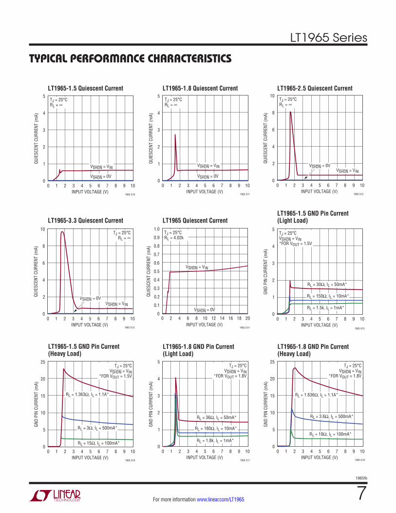
typical perForMance characteristics
LT1965-1.5 Quiescent Current LT1965-1.8 Quiescent Current LT1965-2.5 Quiescent Current
LT1965-3.3 Quiescent Current LT1965 Quiescent CurrentLT1965-1.5 GND Pin Current (Light Load)
LT1965-1.5 GND Pin Current (Heavy Load)
LT1965-1.8 GND Pin Current (Light Load)
LT1965-1.8 GND Pin Current (Heavy Load)
0
QUIE
SCEN
T CU
RREN
T (m
A)
0.2
0.4
0.6
0.8
1.0
0.1
0.3
0.5
0.7
0.9
1965 G14INPUT VOLTAGE (V)
0 164 8 12 20142 6 10 18
TJ = 25°CRL = 4.02k
VSHDN = VIN
VSHDN = 0V
0
QUIE
SCEN
T CU
RREN
T (m
A)
1
3
5
2
4
1965 G10INPUT VOLTAGE (V)
0 1 2 3 4 5 6 7 8 9 10
TJ = 25°CRL = ∞
VSHDN = VIN
VSHDN = 0V0
QUIE
SCEN
T CU
RREN
T (m
A)
1
3
5
2
4
1965 G11INPUT VOLTAGE (V)
0 1 2 3 4 5 6 7 8 9 10
TJ = 25°CRL = ∞
VSHDN = VIN
VSHDN = 0V0
QUIE
SCEN
T CU
RREN
T (m
A)
2
6
10
4
8
1965 G12INPUT VOLTAGE (V)
0 1 2 3 4 5 6 7 8 9 10
TJ = 25°CRL = ∞
VSHDN = VINVSHDN = 0V
0
QUIE
SCEN
T CU
RREN
T (m
A)
2
6
10
4
8
1965 G13INPUT VOLTAGE (V)
0 1 2 3 4 5 6 7 8 9 10
TJ = 25°CRL = ∞
VSHDN = VIN
VSHDN = 0V
0
GND
PIN
CURR
ENT
(mA)
5
15
25
10
20
1965 G16INPUT VOLTAGE (V)
0 1 2 3 4 5 6 7 8 9 10
TJ = 25°CVSHDN = VIN
*FOR VOUT = 1.5V
RL = 3Ω, IL = 500mA*
RL = 15Ω, IL = 100mA*
RL = 1.363Ω, IL = 1.1A*
0
GND
PIN
CURR
ENT
(mA)
1
3
5
2
4
1965 G15INPUT VOLTAGE (V)
0 1 2 3 4 5 6 7 8 9 10
TJ = 25°CVSHDN = VIN*FOR VOUT = 1.5V
RL = 30Ω, IL = 50mA*
RL = 150Ω, IL = 10mA*
RL = 1.5k, IL = 1mA*
0
GND
PIN
CURR
ENT
(mA)
1
3
5
2
4
1965 G17INPUT VOLTAGE (V)
0 1 2 3 4 5 6 7 8 9 10
TJ = 25°CVSHDN = VIN
*FOR VOUT = 1.8V
RL = 36Ω, IL = 50mA*
RL = 180Ω, IL = 10mA*
RL = 1.8k, IL = 1mA*0
GND
PIN
CURR
ENT
(mA)
5
15
25
10
20
1965 G18INPUT VOLTAGE (V)
0 1 2 3 4 5 6 7 8 9 10
TJ = 25°CVSHDN = VIN
*FOR VOUT = 1.8V
RL = 3.6Ω, IL = 500mA*
RL = 18Ω, IL = 100mA*
RL = 1.636Ω, IL = 1.1A*
LT1965 Series
81965fb
For more information www.linear.com/LT1965
typical perForMance characteristics
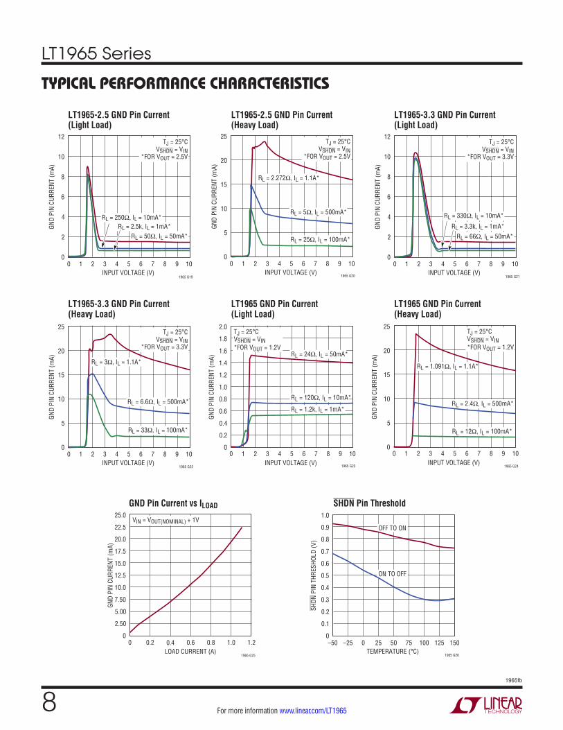
LT1965-2.5 GND Pin Current (Light Load)
LT1965-2.5 GND Pin Current (Heavy Load)
LT1965-3.3 GND Pin Current (Light Load)
LT1965-3.3 GND Pin Current (Heavy Load)
LT1965 GND Pin Current (Light Load)
LT1965 GND Pin Current (Heavy Load)
GND Pin Current vs ILOAD SHDN Pin Threshold
0
GND
PIN
CURR
ENT
(mA)
0.4
0.8
1.2
1.6
2.0
0.2
0.6
1.0
1.4
1.8
1965 G23INPUT VOLTAGE (V)0 82 4 6 1071 3 5 9
TJ = 25°CVSHDN = VIN *FOR VOUT = 1.2V
RL = 24Ω, IL = 50mA*
RL = 120Ω, IL = 10mA*
RL = 1.2k, IL = 1mA*
0
GND
PIN
CURR
ENT
(mA)
5
10
15
20
25
1965 G24INPUT VOLTAGE (V)
0 82 4 6 1071 3 5 9
TJ = 25°CVSHDN = VIN *FOR VOUT = 1.2V
RL = 1.091Ω, IL = 1.1A*
RL = 2.4Ω, IL = 500mA*
RL = 12Ω, IL = 100mA*
LOAD CURRENT (A)0
0
GND
PIN
CURR
ENT
(mA)
5.00
10.0
15.0
0.2 0.4 0.6 0.8 1.0
20.0
25.0
2.50
7.50
12.5
17.5
22.5
1.2
1965 G25
VIN = VOUT(NOMINAL) + 1V
0
SHDN
PIN
THR
ESHO
LD (V
)
0.2
0.4
0.6
0.8
1.0
0.1
0.3
0.5
0.7
0.9
1965 G26TEMPERATURE (°C)
–50 –25 0 25 50 75 125100 150
OFF TO ON
ON TO OFF
0
GND
PIN
CURR
ENT
(mA)
2
4
8
12
6
10
1965 G19INPUT VOLTAGE (V)
0 1 2 3 4 5 6 7 8 9 10
TJ = 25°CVSHDN = VIN
*FOR VOUT = 2.5V
RL = 250Ω, IL = 10mA*
RL = 50Ω, IL = 50mA*RL = 2.5k, IL = 1mA*
0
GND
PIN
CURR
ENT
(mA)
5
15
25
10
20
1965 G20INPUT VOLTAGE (V)
0 1 2 3 4 5 6 7 8 9 10
TJ = 25°CVSHDN = VIN
*FOR VOUT = 2.5V
RL = 5Ω, IL = 500mA*
RL = 25Ω, IL = 100mA*
RL = 2.272Ω, IL = 1.1A*
0
GND
PIN
CURR
ENT
(mA)
2
4
8
12
6
10
1965 G21INPUT VOLTAGE (V)
0 1 2 3 4 5 6 7 8 9 10
TJ = 25°CVSHDN = VIN
*FOR VOUT = 3.3V
RL = 330Ω, IL = 10mA*
RL = 66Ω, IL = 50mA*
RL = 3.3k, IL = 1mA*
0
GND
PIN
CURR
ENT
(mA)
5
15
25
10
20
1965 G22INPUT VOLTAGE (V)
0 1 2 3 4 5 6 7 8 9 10
TJ = 25°CVSHDN = VIN
*FOR VOUT = 3.3V
RL = 6.6Ω, IL = 500mA*
RL = 33Ω, IL = 100mA*
RL = 3Ω, IL = 1.1A*
LT1965 Series
91965fb
For more information www.linear.com/LT1965
typical perForMance characteristics
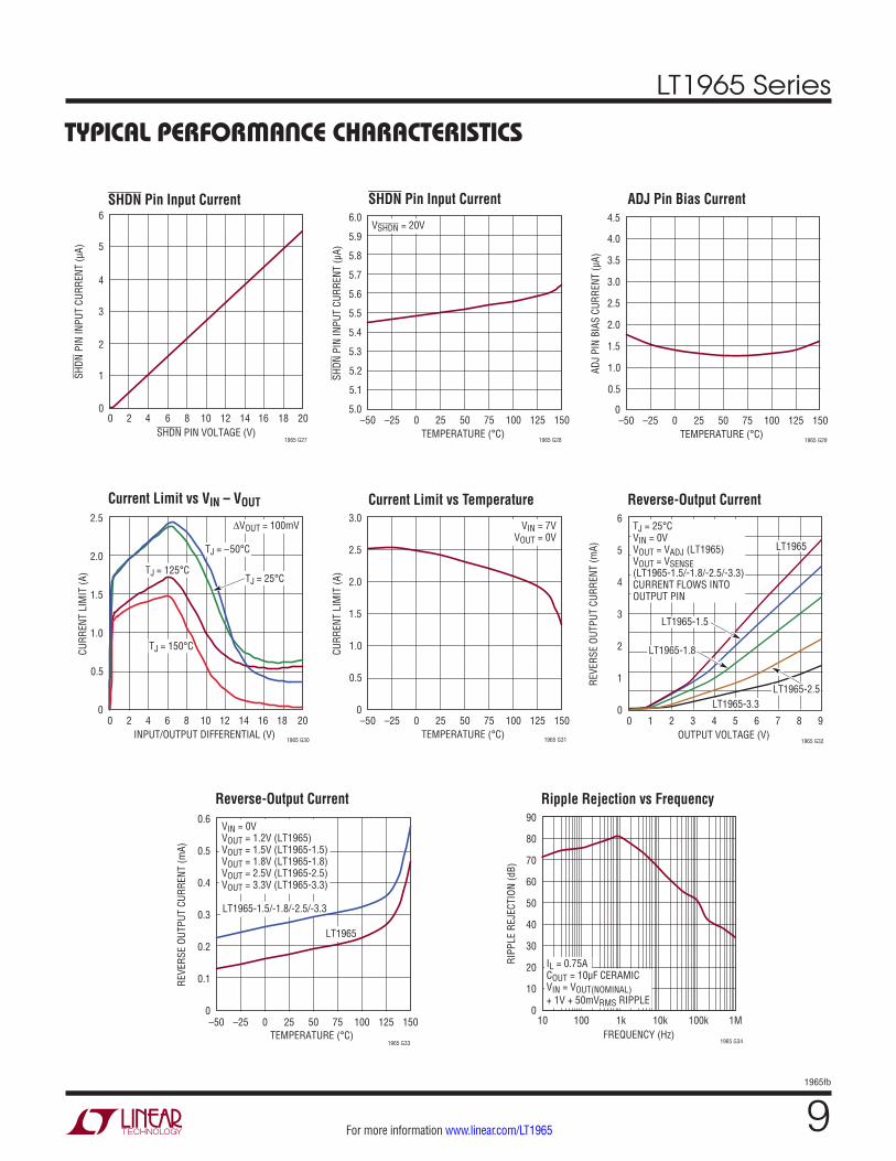
SHDN Pin Input Current ADJ Pin Bias Current
Current Limit vs VIN – VOUT Current Limit vs Temperature Reverse-Output Current
Reverse-Output Current Ripple Rejection vs Frequency
SHDN Pin Input Current
SHDN PIN VOLTAGE (V)
0
SHDN
PIN
INPU
T CU
RREN
T (µ
A)
2
4
6
1
3
5
4 8 12 16 2020 6 10 14 18
1965 G27
5.0
SHDN
PIN
INPU
T CU
RREN
T (µ
A)
5.2
5.4
5.6
5.8
6.0
5.1
5.3
5.5
5.7
5.9
1965 G28TEMPERATURE (°C)
–50 –25 0 25 50 75 125100 150
VSHDN = 20V
0
ADJ
PIN
BIAS
CUR
RENT
(µA)
1.0
2.0
3.0
4.0
4.5
0.5
1.5
2.5
3.5
1965 G29TEMPERATURE (°C)
–50 –25 0 25 50 75 125100 150
0
CURR
ENT
LIM
IT (A
)
0.5
1.5
2.5
1.0
2.0
1965 G30INPUT/OUTPUT DIFFERENTIAL (V)
0 2 4 6 8 10 12 14 16 18 20
∆VOUT = 100mV
TJ = –50°C
TJ = 125°C
TJ = 150°C
TJ = 25°C
0
CURR
ENT
LIM
IT (A
)
1.0
2.0
3.0
0.5
1.5
2.5
1965 G31TEMPERATURE (°C)
–50 –25 0 25 50 75 125100 150
VIN = 7VVOUT = 0V
0
REVE
RSE
OUTP
UT C
URRE
NT (m
A)
2
4
6
1
3
5
1965 G32OUTPUT VOLTAGE (V)
0 1 432 5 6 7 8 9
LT1965
LT1965-1.5
LT1965-1.8
LT1965-3.3
TJ = 25°CVIN = 0VVOUT = VADJ (LT1965)VOUT = VSENSE (LT1965-1.5/-1.8/-2.5/-3.3)CURRENT FLOWS INTOOUTPUT PIN
LT1965-2.5
0
REVE
RSE
OUTP
UT C
URRE
NT (m
A)
0.1
0.5
0.4
0.3
0.2
0.6
1965 G33TEMPERATURE (°C)
LT1965
VIN = 0VVOUT = 1.2V (LT1965)VOUT = 1.5V (LT1965-1.5)VOUT = 1.8V (LT1965-1.8)VOUT = 2.5V (LT1965-2.5)VOUT = 3.3V (LT1965-3.3)
LT1965-1.5/-1.8/-2.5/-3.3
–50 –25 0 25 50 75 125100 150FREQUENCY (Hz)
20
RIPP
LE R
EJEC
TION
(dB)
30
50
60
80
90
10 1k 10k 1M
10
100 100k
70
40
0
1965 G34
IL = 0.75ACOUT = 10µF CERAMICVIN = VOUT(NOMINAL) + 1V + 50mVRMS RIPPLE
LT1965 Series
101965fb
For more information www.linear.com/LT1965
typical perForMance characteristics
Load Regulation
Output Noise Spectral DensityRMS Output Noise vs Load Current (10Hz to 100kHz)
LT1965-1.8 10Hz to 100kHz Output Noise
LT1965-3.3 Transient ResponseLT1965-2.5 SHDN Transient Response
Ripple Rejection vs Temperature LT1965 Minimum Input Voltage
RIPP
LE R
EJEC
TION
(dB)
100
1965 G35TEMPERATURE (°C)
–50 –25 0 25 50 75 125100 1500
20
40
60
80
10
30
50
70
90
IL = 0.75AVIN = VOUT(NOMINAL) + 1V + 0.5P-PRIPPLE AT f = 120Hz
IL = 1.1A
–50 –25 0 25 50 75 125100 1500
MIN
IMUM
INPU
T VO
LTAG
E (V
)
0.5
1.0
1.5
2.0
2.5
1965 G36TEMPERATURE (°C)
IL = 100mA
IL = 1A
IL = 500mA
LOAD
REG
ULAT
ION
(mV)
–30
–25
–20
–15
–50
–45
–40
–35
–10
–5
0
1965 G37TEMPERATURE (°C)
LT1965
VIN = VOUT(NOMINAL) + 1V(LT1965-1.5/-1.8/-2.5/-3.3)VIN = 2.3V (LT1965)∆IL = 1mA TO 1.1A
LT1965-3.3
–50 –25 0 25 50 75 125100 150
LT1965-1.5
LT1965-1.8
LT1965-2.5
0.01
0.10
1.00
FREQUENCY (Hz)
10
OUTP
UT N
OISE
SPE
CTRA
L DE
NSIT
Y (µ
V H
z)
100 1k 10k 100k
1965 G38
LT1965-3.3
LT1965
LT1965-1.5LT1965-1.8
LT1965-2.5
COUT = 10µFIL = 1.1A
LOAD CURRENT (A)
20
OUTP
UT N
OISE
VOL
TAGE
(µV R
MS)
30
50
70
80
0.0001 0.01 0.1 10
10
0.001 1
60
40
0
1965 G39
LT1965-2.5
LT1965-3.3
LT1965-1.8
LT1965
COUT = 10µFIL = 1.1A
LT1965-1.5 400µs/DIV
VOUT100µV/DIV
1965 G40
00
–100
OUTP
UT V
OLTA
GEDE
VIAT
ION
(mV)
LOAD
CUR
RENT
(A)
–50
0
50
100
0.5
1.0
1.5
10 20 30 40 50 60 70 80
1965 G41TIME (µs)
VIN = 4.3VCIN = 10µF CERAMICCOUT = 10µF CERAMIC
VOUT = 3.3V
TIME (µs)0
SHDN
AND
OUT
PUT
VOLT
AGE
(V)
4.0
3.5
3.0
2.5
2.0
1.5
1.0
0.5
08020 40 60 1007010 30 50 90
1965 G42
OUTPUT
SHDN
VIN = 3.3VCOUT = 10µF CERAMICRL = 2.5k, IL = 1mA FOR VOUT = 2.5V
LT1965 Series
111965fb
For more information www.linear.com/LT1965
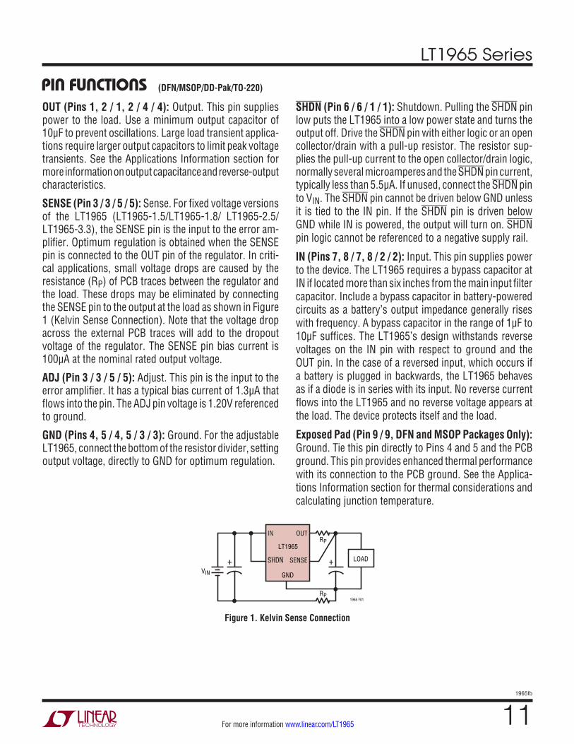
pin FunctionsOUT (Pins 1, 2 / 1, 2 / 4 / 4): Output. This pin supplies power to the load. Use a minimum output capacitor of 10µF to prevent oscillations. Large load transient applica-tions require larger output capacitors to limit peak voltage transients. See the Applications Information section for more information on output capacitance and reverse-output characteristics.
SENSE (Pin 3 / 3 / 5 / 5): Sense. For fixed voltage versions of the LT1965 (LT1965-1.5/LT1965-1.8/ LT1965-2.5/ LT1965-3.3), the SENSE pin is the input to the error am-plifier. Optimum regulation is obtained when the SENSE pin is connected to the OUT pin of the regulator. In criti-cal applications, small voltage drops are caused by the resistance (RP) of PCB traces between the regulator and the load. These drops may be eliminated by connecting the SENSE pin to the output at the load as shown in Figure 1 (Kelvin Sense Connection). Note that the voltage drop across the external PCB traces will add to the dropout voltage of the regulator. The SENSE pin bias current is 100µA at the nominal rated output voltage.
ADJ (Pin 3 / 3 / 5 / 5): Adjust. This pin is the input to the error amplifier. It has a typical bias current of 1.3µA that flows into the pin. The ADJ pin voltage is 1.20V referenced to ground.
GND (Pins 4, 5 / 4, 5 / 3 / 3): Ground. For the adjustable LT1965, connect the bottom of the resistor divider, setting output voltage, directly to GND for optimum regulation.
SHDN (Pin 6 / 6 / 1 / 1): Shutdown. Pulling the SHDN pin low puts the LT1965 into a low power state and turns the output off. Drive the SHDN pin with either logic or an open collector/drain with a pull-up resistor. The resistor sup-plies the pull-up current to the open collector/drain logic, normally several microamperes and the SHDN pin current, typically less than 5.5µA. If unused, connect the SHDN pin to VIN. The SHDN pin cannot be driven below GND unless it is tied to the IN pin. If the SHDN pin is driven below GND while IN is powered, the output will turn on. SHDN pin logic cannot be referenced to a negative supply rail.
IN (Pins 7, 8 / 7, 8 / 2 / 2): Input. This pin supplies power to the device. The LT1965 requires a bypass capacitor at IN if located more than six inches from the main input filter capacitor. Include a bypass capacitor in battery-powered circuits as a battery’s output impedance generally rises with frequency. A bypass capacitor in the range of 1µF to 10µF suffices. The LT1965’s design withstands reverse voltages on the IN pin with respect to ground and the OUT pin. In the case of a reversed input, which occurs if a battery is plugged in backwards, the LT1965 behaves as if a diode is in series with its input. No reverse current flows into the LT1965 and no reverse voltage appears at the load. The device protects itself and the load.
Exposed Pad (Pin 9 / 9, DFN and MSOP Packages Only): Ground. Tie this pin directly to Pins 4 and 5 and the PCB ground. This pin provides enhanced thermal performance with its connection to the PCB ground. See the Applica-tions Information section for thermal considerations and calculating junction temperature.
(DFN/MSOP/DD-Pak/TO-220)
Figure 1. Kelvin Sense Connection
IN
1965 F01
RP
RP
OUT
VIN
SENSESHDN
GND
LT1965
+ + LOAD
LT1965 Series
121965fb
For more information www.linear.com/LT1965
applications inForMationThe LT1965 series are 1.1A low dropout regulators with shutdown. The devices are capable of supplying 1.1A at a typical dropout voltage of 310mV. The low operating quiescent current (500µA for the adjustable version, 600µA for the fixed voltage versions) drops to less than 1µA in shutdown. In addition to the low quiescent current, the LT1965 regulators incorporate several protection features that makes them ideal for use in battery-powered systems. The devices protect themselves against both reverse-input and reverse-output voltages. In battery backup applica-tions, if a backup battery holds up the output when the input is pulled to ground, the LT1965 performs like it has a diode in series with its output, preventing reverse-current flow.
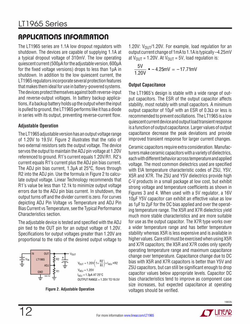
Adjustable Operation
The LT1965 adjustable version has an output voltage range of 1.20V to 19.5V. Figure 2 illustrates that the ratio of two external resistors sets the output voltage. The device servos the output to maintain the ADJ pin voltage at 1.20V referenced to ground. R1’s current equals 1.20V/R1. R2’s current equals R1’s current plus the ADJ pin bias current. The ADJ pin bias current, 1.3µA at 25°C, flows through R2 into the ADJ pin. Use the formula in Figure 2 to calcu-late output voltage. Linear Technology recommends that R1’s value be less than 12.1k to minimize output voltage errors due to the ADJ pin bias current. In shutdown, the output turns off and the divider current is zero. For curves depicting ADJ Pin Voltage vs Temperature and ADJ Pin Bias Current vs Temperature, see the Typical Performance Characteristics section.
The adjustable device is tested and specified with the ADJ pin tied to the OUT pin for an output voltage of 1.20V. Specifications for output voltages greater than 1.20V are proportional to the ratio of the desired output voltage to
1.20V: VOUT/1.20V. For example, load regulation for an output current change of 1mA to 1.1A is typically –4.25mV at VOUT = 1.20V. At VOUT = 5V, load regulation is:
5V1.20V
• – 4.25mV = – 17.71mV
Output Capacitance
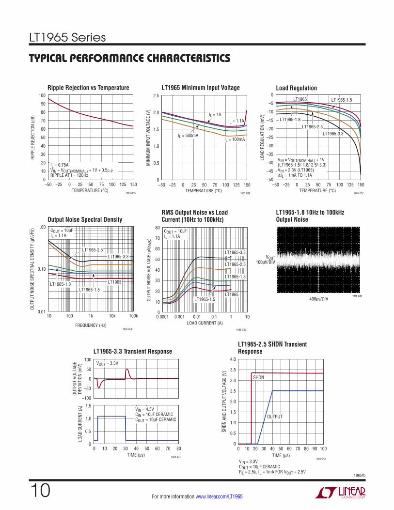
The LT1965’s design is stable with a wide range of out-put capacitors. The ESR of the output capacitor affects stability, most notably with small capacitors. A minimum output capacitor of 10µF with an ESR of 0.3W or less is recommended to prevent oscillations. The LT1965 is a low quiescent current device and output load transient response is a function of output capacitance. Larger values of output capacitance decrease the peak deviations and provide improved transient response for larger current changes.
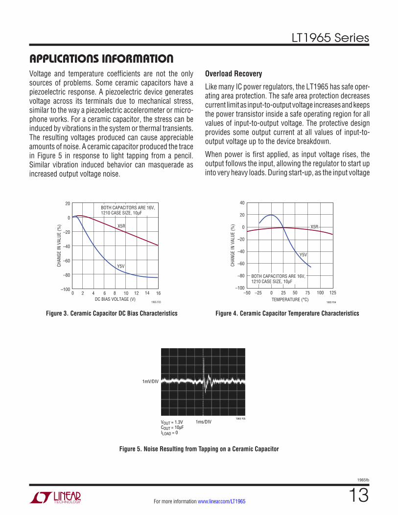
Ceramic capacitors require extra consideration. Manufac-turers make ceramic capacitors with a variety of dielectrics, each with different behavior across temperature and applied voltage. The most common dielectrics used are specified with EIA temperature characteristic codes of Z5U, Y5V, X5R and X7R. The Z5U and Y5V dielectrics provide high C-V products in a small package at low cost, but exhibit strong voltage and temperature coefficients as shown in Figures 3 and 4. When used with a 5V regulator, a 16V 10µF Y5V capacitor can exhibit an effective value as low as 1µF to 2µF for the DC bias applied and over the operat-ing temperature range. The X5R and X7R dielectrics yield much more stable characteristics and are more suitable for use as the output capacitor. The X7R type works over a wider temperature range and has better temperature stability whereas X5R is less expensive and is available in higher values. Care still must be exercised when using X5R and X7R capacitors; the X5R and X7R codes only specify operating temperature range and maximum capacitance change over temperature. Capacitance change due to DC bias with X5R and X7R capacitors is better than Y5V and Z5U capacitors, but can still be significant enough to drop capacitor values below appropriate levels. Capacitor DC bias characteristics tend to improve as component case size increases, but expected capacitance at operating voltages should be verified. Figure 2. Adjustable Operation
IN
1965 F02
R2
OUT
VIN
VOUT
ADJ
GND
LT1965
R1
+
VOUT = 1.20V 1+ R2R1
+ IADJ •R2
VADJ = 1.20VIADJ = 1.3µA AT 25ºCOUTPUT RANGE = 1.20V TO 19.5V
LT1965 Series
131965fb
For more information www.linear.com/LT1965
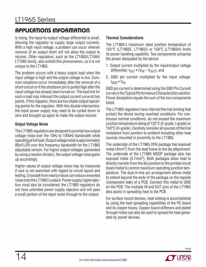
applications inForMationVoltage and temperature coefficients are not the only sources of problems. Some ceramic capacitors have a piezoelectric response. A piezoelectric device generates voltage across its terminals due to mechanical stress, similar to the way a piezoelectric accelerometer or micro-phone works. For a ceramic capacitor, the stress can be induced by vibrations in the system or thermal transients. The resulting voltages produced can cause appreciable amounts of noise. A ceramic capacitor produced the trace in Figure 5 in response to light tapping from a pencil. Similar vibration induced behavior can masquerade as increased output voltage noise.
Overload Recovery
Like many IC power regulators, the LT1965 has safe oper-ating area protection. The safe area protection decreases current limit as input-to-output voltage increases and keeps the power transistor inside a safe operating region for all values of input-to-output voltage. The protective design provides some output current at all values of input-to-output voltage up to the device breakdown.
When power is first applied, as input voltage rises, the output follows the input, allowing the regulator to start up into very heavy loads. During start-up, as the input voltage
Figure 3. Ceramic Capacitor DC Bias Characteristics Figure 4. Ceramic Capacitor Temperature Characteristics
Figure 5. Noise Resulting from Tapping on a Ceramic Capacitor
DC BIAS VOLTAGE (V)
CHAN
GE IN
VAL
UE (%
)
1965 F03
20
0
–20
–40
–60
–80
–1000 4 8 102 6 12 14
X5R
Y5V
16
BOTH CAPACITORS ARE 16V,1210 CASE SIZE, 10µF
TEMPERATURE (°C)–50
40
20
0
–20
–40
–60
–80
–10025 75
1965 F04
–25 0 50 100 125
Y5V
CHAN
GE IN
VAL
UE (%
) X5R
BOTH CAPACITORS ARE 16V,1210 CASE SIZE, 10µF
1ms/DIV
1mV/DIV
1965 F05
VOUT = 1.3VCOUT = 10µFILOAD = 0
LT1965 Series
141965fb
For more information www.linear.com/LT1965
is rising, the input-to-output voltage differential is small, allowing the regulator to supply large output currents. With a high input voltage, a problem can occur wherein removal of an output short will not allow the output to recover. Other regulators, such as the LT1083/LT1084/LT1085 family, also exhibit this phenomenon, so it is not unique to the LT1965.
The problem occurs with a heavy output load when the input voltage is high and the output voltage is low. Com-mon situations occur immediately after the removal of a short-circuit or if the shutdown pin is pulled high after the input voltage has already been turned on. The load line for such a load may intersect the output current curve at two points. If this happens, there are two stable output operat-ing points for the regulator. With this double intersection, the input power supply may need to be cycled down to zero and brought up again to make the output recover.
Output Voltage Noise
The LT1965 regulators are designed to provide low output voltage noise over the 10Hz to 100kHz bandwidth while operating at full load. Output voltage noise is approximately 80nV/√Hz over this frequency bandwidth for the LT1965 adjustable version. For higher output voltages (generated by using a resistor divider), the output voltage noise gains up accordingly.
Higher values of output voltage noise may be measured if care is not exercised with regard to circuit layout and testing. Crosstalk from nearby traces can induce unwanted noise onto the LT1965’s output. Power supply ripple rejec-tion must also be considered; the LT1965 regulators do not have unlimited power supply rejection and will pass a small portion of the input noise through to the output.
applications inForMationThermal Considerations
The LT1965’s maximum rated junction temperature of 125°C (LT1965E, LT1965I) or 150°C (LT1965H) limits its power handling capability. Two components comprise the power dissipated by the device:
1. Output current multiplied by the input/output voltage differential: IOUT • (VIN – VOUT), and
2. GND pin current multiplied by the input voltage: IGND • VIN
GND pin current is determined using the GND Pin Current curves in the Typical Performance Characteristics section. Power dissipation equals the sum of the two components listed.
The LT1965 regulators have internal thermal limiting that protect the device during overload conditions. For con-tinuous normal conditions, do not exceed the maximum junction temperature rating of 125°C (E-grade, I-grade) or 150°C (H-grade). Carefully consider all sources of thermal resistance from junction to ambient including other heat sources mounted in proximity to the LT1965.
The underside of the LT1965 DFN package has exposed metal (4mm2) from the lead frame to the die attachment. The underside of the LT1965 MSOP package also has exposed metal (3.7mm2). Both packages allow heat to directly transfer from the die junction to the printed circuit board metal to control maximum operating junction tem-perature. The dual-in-line pin arrangement allows metal to extend beyond the ends of the package on the topside (component side) of a PCB. Connect this metal to GND on the PCB. The multiple IN and OUT pins of the LT1965 also assist in spreading heat to the PCB.
For surface mount devices, heat sinking is accomplished by using the heat spreading capabilities of the PC board and its copper traces. Copper board stiffeners and plated through-holes can also be used to spread the heat gener-ated by power devices.
LT1965 Series
151965fb
For more information www.linear.com/LT1965
applications inForMationThe following tables list thermal resistance for several different board sizes and copper areas. All measurements were taken in still air on a 2-layer 1/16" FR-4 board with one ounce copper.Table 1. Measured Thermal Resistance for DFN Package
Copper Area Thermal ResistanceTopside* Backside Board Area (Junction-to-Ambient)2500mm2 2500mm2 2500mm2 60°C/W1000mm2 2500mm2 2500mm2 62°C/W225mm2 2500mm2 2500mm2 65°C/W100mm2 2500mm2 2500mm2 68°C/W50mm2 2500mm2 2500mm2 70°C/W
*Device is mounted on topside
Table 2. Measured Thermal Resistance for MSOP PackageCopper Area Thermal Resistance
Topside* Backside Board Area (Junction-to-Ambient)2500mm2 2500mm2 2500mm2 55°C/W1000mm2 2500mm2 2500mm2 57°C/W225mm2 2500mm2 2500mm2 60°C/W100mm2 2500mm2 2500mm2 65°C/W50mm2 2500mm2 2500mm2 68°C/W
*Device is mounted on topside
Table 3. Measured Thermal Resistance for DD-Pak PackageCopper Area Thermal Resistance
Topside* Backside Board Area (Junction-to-Ambient)2500mm2 2500mm2 2500mm2 25°C/W1000mm2 2500mm2 2500mm2 30°C/W125mm2 2500mm2 2500mm2 35°C/W
*Device is mounted on topside
Measured Thermal Resistance for TO-220 Package
Thermal Resistance (Junction-to-Case) = 3°C/W
Calculating Junction Temperature
Example: Given an output voltage of 2.5V, an input volt-age range of 3.3V ± 5%, an output current range of 0mA to 500mA and a maximum ambient temperature of 85°C, what will the maximum junction temperature be?
The power dissipated by the device equals:
IOUT(MAX) • (VIN(MAX) – VOUT) + IGND • VIN(MAX)
where:
IOUT(MAX) = 500mA
VIN(MAX) = 3.465V
IGND at (IOUT = 500mA, VIN = 3.465V) = 8.2mA
So,
P = 500mA(3.465V – 2.5V) + 8.2mA(3.465V) = 0.511W
Using a DFN package, the thermal resistance will be in the range of 60°C/W to 70°C/W depending on the cop-per area. So the junction temperature rise above ambient approximately equals:
0.511W • 65°C/W = 33.22°C
The maximum junction temperature equals the maximum ambient temperature plus the maximum junction tempera-ture rise above ambient or:
TJMAX = 85°C + 33.22°C = 118.22°C
Protection Features
The LT1965 regulators incorporate several protection features that makes them ideal for use in battery-powered circuits. In addition to the normal protection features associated with monolithic regulators, such as current limiting and thermal limiting, the devices also protect against reverse-input voltages, reverse-output voltages and reverse output-to-input voltages.
Current-limit protection and thermal overload protection protect the device against current overload conditions at its output. For normal operation, do not exceed the maximum rated junction temperature of 125°C (LT1965E, LT1965I) or 150°C (LT1965H).
LT1965 Series
161965fb
For more information www.linear.com/LT1965
The input of the device withstands reverse voltages of 22V. The LT1965 limits current flow to less than 1mA (typically less than 300µA) and no negative voltage appears at the output. The device protects both itself and the load against batteries that are plugged in backwards.
The LT1965 incurs no damage if its output is pulled be-low ground. If the input is left open-circuit or grounded, the output can be pulled below ground by 22V. For fixed voltage versions, the output will act like a large resistor, typically 5k or higher, limiting current flow to typically less than 300µA. For the adjustable version, the output acts like an open circuit and no current flows from the output. However, current flows out of (but is limited by) the resistor divider that sets the output voltage. If the input is powered by a voltage source, the LT1965 protects itself by shutting off the output.
The LT1965 adjustable version incurs no damage if the ADJ pin is pulled above or below ground by 9V. If the input is left open-circuit or grounded, the ADJ pin performs like a diode in series with typically 1.5k of resistance when pulled below ground and like a large resistor (typically 5k up to 3V on the ADJ pin and then 1.5k up to 9V) in series with a diode when pulled above ground.
In situations where the ADJ pin connects to a resistor divider that would pull the ADJ pin above its 9V clamp
voltage if the output is pulled high, the ADJ pin input current must be limited to less than 5mA. For example, a resistor divider is used to provide a regulated 1.5V output from the 1.20V reference when the output is forced to 20V. The top resistor of the resistor divider must be chosen to limit the current into the ADJ pin to less than 5mA when the ADJ pin is at 9V. The 11V difference between the OUT and ADJ pins divided by the 5mA maximum current into the ADJ pin yields a minimum top resistor value of 2.2k.
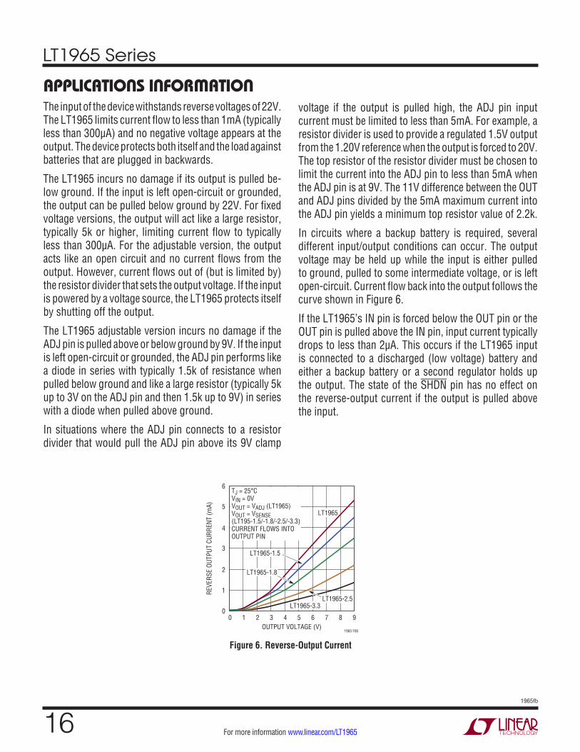
In circuits where a backup battery is required, several different input/output conditions can occur. The output voltage may be held up while the input is either pulled to ground, pulled to some intermediate voltage, or is left open-circuit. Current flow back into the output follows the curve shown in Figure 6.
If the LT1965’s IN pin is forced below the OUT pin or the OUT pin is pulled above the IN pin, input current typically drops to less than 2µA. This occurs if the LT1965 input is connected to a discharged (low voltage) battery and either a backup battery or a second regulator holds up the output. The state of the SHDN pin has no effect on the reverse-output current if the output is pulled above the input.
Figure 6. Reverse-Output Current
applications inForMation
OUTPUT VOLTAGE (V)0
0
REVE
RSE
OUTP
UT C
URRE
NT (m
A)
1
2
3
4
5
6
21 43 65 87 9
1965 F06
LT1965
LT1965-1.5
LT1965-3.3
TJ = 25°CVIN = 0VVOUT = VADJ (LT1965)VOUT = VSENSE (LT195-1.5/-1.8/-2.5/-3.3)CURRENT FLOWS INTOOUTPUT PIN
LT1965-2.5
LT1965-1.8
LT1965 Series
171965fb
For more information www.linear.com/LT1965
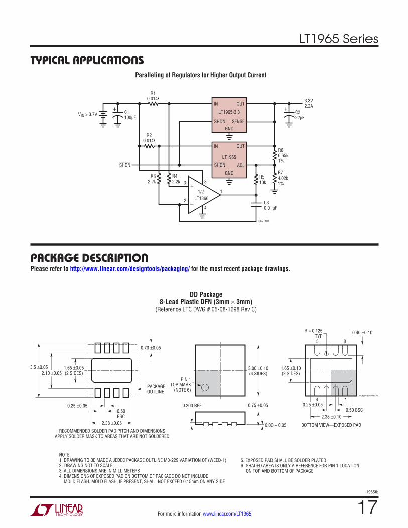
typical applicationsParalleling of Regulators for Higher Output Current
package DescriptionPlease refer to http://www.linear.com/designtools/packaging/ for the most recent package drawings.
R10.01Ω
R20.01Ω
R510k
R42.2k
R74.02k1%
C222µF
1965 TA03
VIN > 3.7V
3.3V2.2A
8
1
3
2
4C30.01µF
IN OUT
SENSEGND
LT1965-3.3
SHDN
IN
SHDN
OUT
ADJ
GND
LT1965
SHDN
+C1100µF
+
–
+1/2
LT1366
R66.65k1%
R32.2k
3.00 ±0.10(4 SIDES)
NOTE:1. DRAWING TO BE MADE A JEDEC PACKAGE OUTLINE M0-229 VARIATION OF (WEED-1)2. DRAWING NOT TO SCALE3. ALL DIMENSIONS ARE IN MILLIMETERS4. DIMENSIONS OF EXPOSED PAD ON BOTTOM OF PACKAGE DO NOT INCLUDE MOLD FLASH. MOLD FLASH, IF PRESENT, SHALL NOT EXCEED 0.15mm ON ANY SIDE
5. EXPOSED PAD SHALL BE SOLDER PLATED6. SHADED AREA IS ONLY A REFERENCE FOR PIN 1 LOCATION ON TOP AND BOTTOM OF PACKAGE
0.40 ±0.10
BOTTOM VIEW—EXPOSED PAD
1.65 ±0.10(2 SIDES)
0.75 ±0.05
R = 0.125TYP
2.38 ±0.10
14
85
PIN 1TOP MARK
(NOTE 6)
0.200 REF
0.00 – 0.05
(DD8) DFN 0509 REV C
0.25 ±0.05
2.38 ±0.05
RECOMMENDED SOLDER PAD PITCH AND DIMENSIONSAPPLY SOLDER MASK TO AREAS THAT ARE NOT SOLDERED
1.65 ±0.05(2 SIDES)2.10 ±0.05
0.50BSC
0.70 ±0.05
3.5 ±0.05
PACKAGEOUTLINE
0.25 ±0.050.50 BSC
DD Package8-Lead Plastic DFN (3mm × 3mm)
(Reference LTC DWG # 05-08-1698 Rev C)
LT1965 Series
181965fb
For more information www.linear.com/LT1965
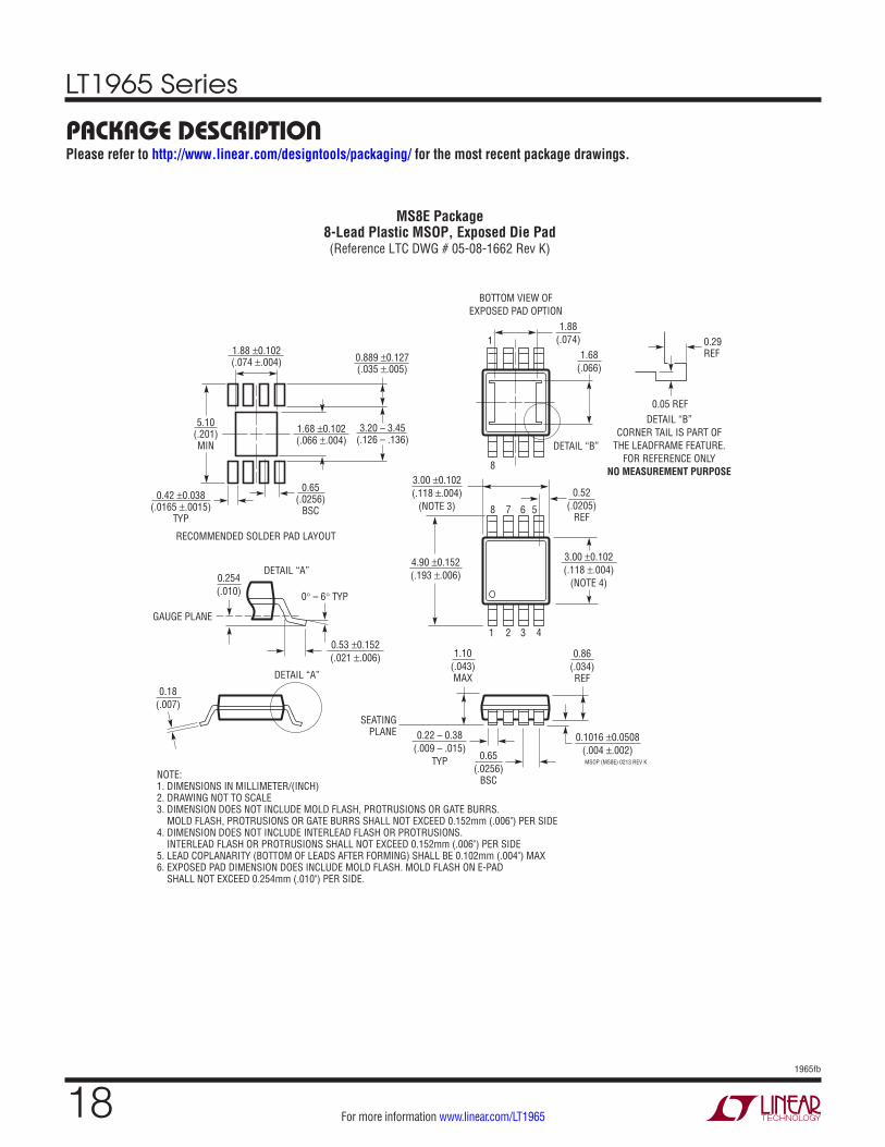
package DescriptionPlease refer to http://www.linear.com/designtools/packaging/ for the most recent package drawings.
MSOP (MS8E) 0213 REV K
0.53 ±0.152(.021 ±.006)
SEATINGPLANE
NOTE:1. DIMENSIONS IN MILLIMETER/(INCH)2. DRAWING NOT TO SCALE3. DIMENSION DOES NOT INCLUDE MOLD FLASH, PROTRUSIONS OR GATE BURRS. MOLD FLASH, PROTRUSIONS OR GATE BURRS SHALL NOT EXCEED 0.152mm (.006") PER SIDE4. DIMENSION DOES NOT INCLUDE INTERLEAD FLASH OR PROTRUSIONS. INTERLEAD FLASH OR PROTRUSIONS SHALL NOT EXCEED 0.152mm (.006") PER SIDE5. LEAD COPLANARITY (BOTTOM OF LEADS AFTER FORMING) SHALL BE 0.102mm (.004") MAX6. EXPOSED PAD DIMENSION DOES INCLUDE MOLD FLASH. MOLD FLASH ON E-PAD SHALL NOT EXCEED 0.254mm (.010") PER SIDE.
0.18(.007)
0.254(.010)
1.10(.043)MAX
0.22 – 0.38(.009 – .015)
TYP
0.86(.034)REF
0.65(.0256)
BSC
0° – 6° TYP
DETAIL “A”
DETAIL “A”
GAUGE PLANE
1 2 3 4
4.90 ±0.152(.193 ±.006)
8
8
1
BOTTOM VIEW OFEXPOSED PAD OPTION
7 6 5
3.00 ±0.102(.118 ±.004)
(NOTE 3)
3.00 ±0.102(.118 ±.004)
(NOTE 4)
0.52(.0205)
REF
1.68(.066)
1.88(.074)
5.10(.201)MIN
3.20 – 3.45(.126 – .136)
1.68 ±0.102(.066 ±.004)
1.88 ±0.102(.074 ±.004) 0.889 ±0.127
(.035 ±.005)
RECOMMENDED SOLDER PAD LAYOUT
0.65(.0256)
BSC0.42 ±0.038
(.0165 ±.0015)TYP
0.1016 ±0.0508(.004 ±.002)
DETAIL “B”
DETAIL “B”CORNER TAIL IS PART OF
THE LEADFRAME FEATURE.FOR REFERENCE ONLY
NO MEASUREMENT PURPOSE
0.05 REF
0.29REF
MS8E Package8-Lead Plastic MSOP, Exposed Die Pad(Reference LTC DWG # 05-08-1662 Rev K)
LT1965 Series
191965fb
For more information www.linear.com/LT1965
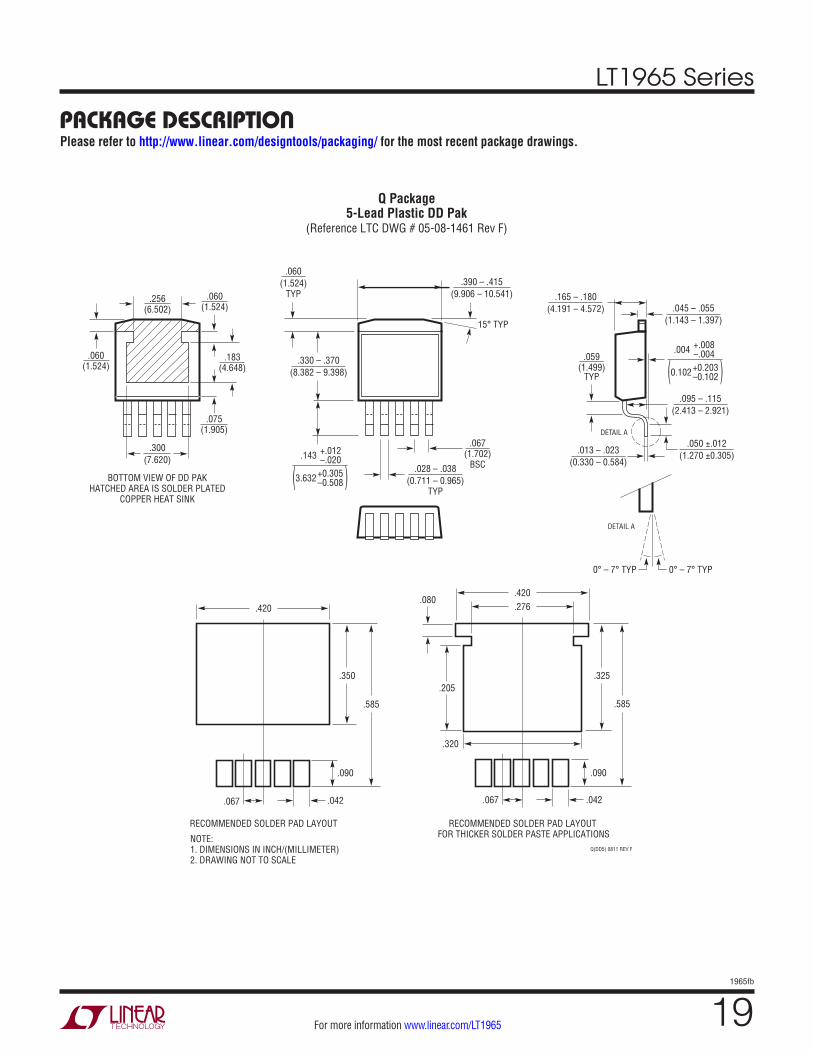
package DescriptionPlease refer to http://www.linear.com/designtools/packaging/ for the most recent package drawings.
Q(DD5) 0811 REV F
.028 – .038(0.711 – 0.965)
TYP
.143 +.012–.020
( )3.632+0.305–0.508
.067(1.702)
BSC.013 – .023
(0.330 – 0.584)
.095 – .115(2.413 – 2.921)
.004 +.008–.004
( )0.102+0.203–0.102
.050 ±.012(1.270 ±0.305)
.059(1.499)
TYP
.045 – .055(1.143 – 1.397)
.165 – .180(4.191 – 4.572)
.330 – .370(8.382 – 9.398)
.060(1.524)
TYP.390 – .415
(9.906 – 10.541)
15° TYP
.420
.350
.585
.090
.042.067
RECOMMENDED SOLDER PAD LAYOUT
.325.205
.080
.585
.090
RECOMMENDED SOLDER PAD LAYOUT FOR THICKER SOLDER PASTE APPLICATIONS
.042.067
.420
.276
.320
NOTE:1. DIMENSIONS IN INCH/(MILLIMETER)2. DRAWING NOT TO SCALE
.300(7.620)
.075(1.905)
.183(4.648)
.060(1.524)
.060(1.524)
.256(6.502)
BOTTOM VIEW OF DD PAKHATCHED AREA IS SOLDER PLATED
COPPER HEAT SINK
Q Package5-Lead Plastic DD Pak
(Reference LTC DWG # 05-08-1461 Rev F)
DETAIL A
DETAIL A
0° – 7° TYP0° – 7° TYP
LT1965 Series
201965fb
For more information www.linear.com/LT1965
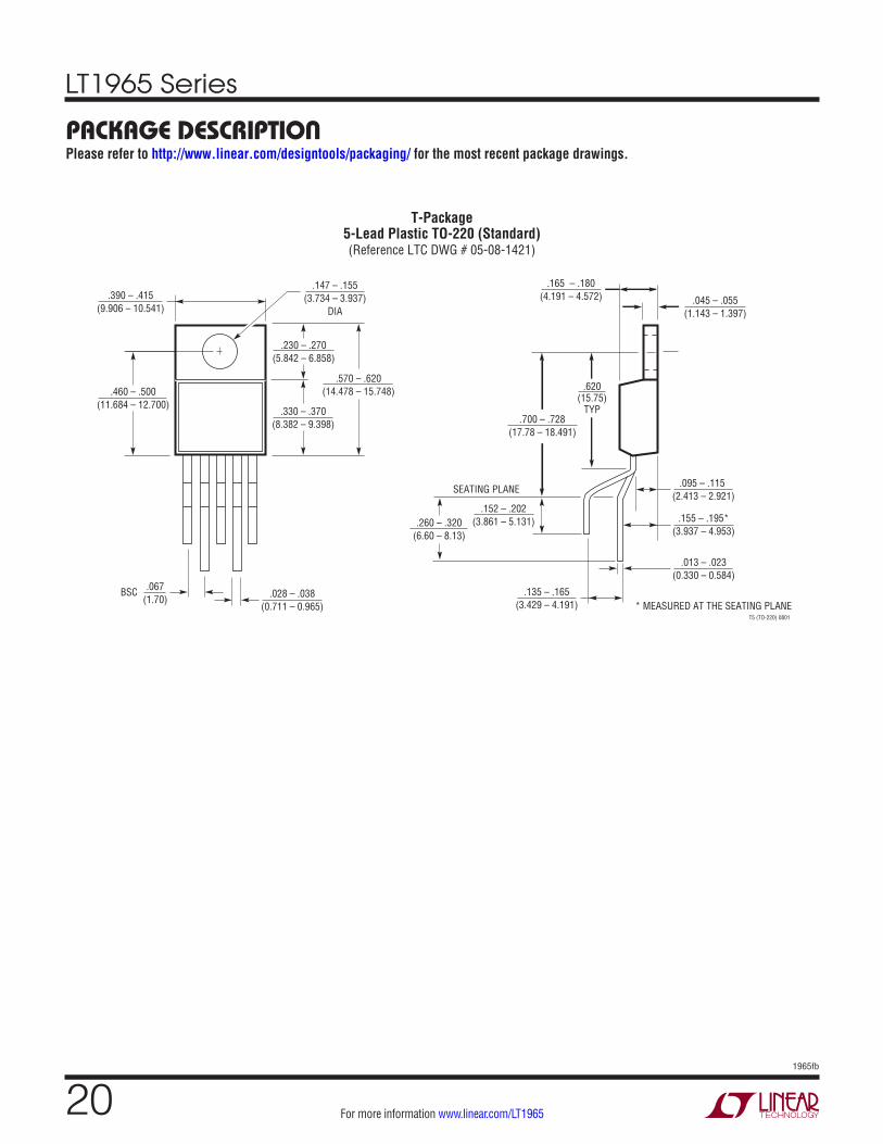
package DescriptionPlease refer to http://www.linear.com/designtools/packaging/ for the most recent package drawings.
T5 (TO-220) 0801
.028 – .038(0.711 – 0.965)
.067(1.70)
.135 – .165(3.429 – 4.191)
.700 – .728(17.78 – 18.491)
.045 – .055(1.143 – 1.397)
.095 – .115 (2.413 – 2.921)
.013 – .023(0.330 – 0.584)
.620(15.75)
TYP
.155 – .195*(3.937 – 4.953)
.152 – .202(3.861 – 5.131).260 – .320
(6.60 – 8.13)
.165 – .180(4.191 – 4.572)
.147 – .155(3.734 – 3.937)
DIA
.390 – .415(9.906 – 10.541)
.330 – .370(8.382 – 9.398)
.460 – .500(11.684 – 12.700)
.570 – .620(14.478 – 15.748)
.230 – .270(5.842 – 6.858)
BSC
SEATING PLANE
* MEASURED AT THE SEATING PLANE
T-Package5-Lead Plastic TO-220 (Standard)(Reference LTC DWG # 05-08-1421)
LT1965 Series
211965fb
For more information www.linear.com/LT1965
Information furnished by Linear Technology Corporation is believed to be accurate and reliable. However, no responsibility is assumed for its use. Linear Technology Corporation makes no representa-tion that the interconnection of its circuits as described herein will not infringe on existing patent rights.
revision historyREV DATE DESCRIPTION PAGE NUMBER
B 08/13 Added H-grade, specs and curves 2-10
Lowered max ESR to 0.3Ω 12
Removed references to “starting up from negative output” 11, 12, 16
(Revision history begins at Rev B)
LT1965 Series
221965fb
For more information www.linear.com/LT1965 LINEAR TECHNOLOGY CORPORATION 2007
LT 0813 REV B • PRINTED IN USALinear Technology Corporation1630 McCarthy Blvd., Milpitas, CA 95035-7417(408) 432-1900 FAX: (408) 434-0507 www.linear.com/LT1965
typical application
PART NUMBER DESCRIPTION COMMENTS
LT1129 700mA, Micropower, LDO VIN: 4.2V to 30V, VOUT(MIN) = 3.8V, VDO = 0.40V, IQ = 50µA, ISD = 16µA; DD, SOT-223, S8, TO220-5 and TSSOP20 Packages
LT1761 100mA, Low Noise Micropower, LDO VIN: 1.8V to 20V, VOUT(MIN) = 1.22V, VDO = 0.30V, IQ = 20µA, ISD = < 1µA, Low Noise < 20µVRMS, Stable with 1µF Ceramic Capacitors, ThinSOT™ Package
LT1762 150mA, Low Noise Micropower, LDO VIN: 1.8V to 20V, VOUT(MIN) = 1.22V, VDO = 0.30V, IQ = 25µA, ISD = < 1µA, Low Noise < 20µVRMS, MS8 Package
LT1763 500mA, Low Noise Micropower, LDO VIN: 1.8V to 20V, VOUT(MIN) = 1.22V, VDO = 0.30V, IQ = 30µA, ISD = < 1µA, Low Noise < 20µVRMS, S8 Package
LT1764/LT1764A
3A, Low Noise, Fast Transient Response, LDO
VIN: 2.7V to 20V, VOUT(MIN) = 1.21V, VDO = 0.34V, IQ = 1mA, ISD = < 1µA, Low Noise < 40µVRMS, “A” Version Stable with Ceramic Capacitors, DD and TO220-5 Packages
LTC1844 150mA, Very Low Drop-Out LDO VIN: 1.6V to 6.5V, VOUT(MIN) = 1.25V, VDO = 0.08V, IQ = 35µA, ISD = < 1µA, Low Noise < 60µVRMS, ThinSOT™ Package
LT1962 300mA, Low Noise Micropower, LDO VIN: 1.8V to 20V, VOUT(MIN) = 1.22V, VDO = 0.27V, IQ = 30µA, ISD = < 1µA, Low Noise < 20µVRMS, MS8 Package
LT1963/LT1963A
1.5A, Low Noise, Fast Transient Response, LDO
VIN: 2.1V to 20V, VOUT(MIN) = 1.21V, VDO = 0.34V, IQ = 1mA, ISD = < 1µA, Low Noise < 40µVRMS, “A” Version Stable with Ceramic Capacitors; DD, TO220-5, SOT-223 and S8 Packages
LT3020 100mA, Low Voltage VDO, VIN(MIN) = 0.9V, LDO
VIN: 0.9V to 10V, VOUT(MIN) = 0.20V, VDO = 0.15V, IQ = 120µA, ISD = 3µA, DFN and MS8 Packages
LT3021 500mA, Low Voltage VDO, VIN(MIN) = 0.9V, LDO
VIN: 0.9V to 10V, VOUT(MIN) = 0.20V, VDO = 0.16V, IQ = 120µA, ISD = 3µA, DFN and S8 Packages
LT3023 Dual, 2x 100mA, Low Noise Micropower, LDO
VIN: 1.8V to 20V, VOUT(MIN) = 1.22V, VDO = 0.30V, IQ = 40µA, ISD = < 1µA, DFN and MS10 Packages
LT3024 Dual, 100mA/500mA, Low Noise Micropower, LDO
VIN: 1.8V to 20V, VOUT(MIN) = 1.22V, VDO = 0.30V, IQ = 60µA, ISD = < 1µA, DFN and TSSOP Packages
LT3027 Dual, 2x 100mA, Low Noise Micropower, LDO with Independent Inputs
VIN: 1.8V to 20V, VOUT(MIN) = 1.22V, VDO = 0.30V, IQ = 25µA, ISD = < 1µA, Low Noise < 20µVRMS, DFN and MS10 Packages
LT3028 Dual, 100mA/500mA, Low Noise Micropower, LDO with Independent Inputs
VIN: 1.8V to 20V, VOUT(MIN) = 1.22V, VDO = 0.30V, IQ = 30µA, ISD = < 1µA, Low Noise < 20µVRMS, DFN and TSSOP Packages
LT3080/LT3080-1
1.1A Parallelable, Low Noise, Low Dropout Linear Regulator
300mV Dropout Voltage (2-Supply Operation), Low Noise: 40µVRMS, VIN: 1.2V to 36V, VOUT: 0V to 35.7V, Current-Based Reference with 1-Resistor VOUT Set; Directly Parallelable (No Op Amp Required), Stable with Ceramic Caps, TO-220, SOT-223, MSOP and 3mm × 3mm DFN Packages; LT3080-1 Version Has Integrated Internal Ballast Resistor
Adjustable Current Source
relateD parts
+
LT1004-1.2VIN > 2.7V C1
10µF
+ C410µF
R32k
R11k
R280.6k
R42.2k
R5, 0.01Ω
R62.2k
LT1965IN
SHDN
OUT
ADJGND
–
+
1/2LT1366
R8100k
LOAD
R7470Ω
2
1
8
34
C31µF
C23.3µF
1965 TA04
NOTE: ADJUST R1 FOR 0A TO 1.1A CONSTANT-CURRENT


