
COLLEGE DE FRANCE Laboratoire de Physique Corpusculaire
Measurement of EMI and HAMAMA TSU photomultiplier characteristics
for the CHOOZ experiment.
P. Salin I and S. Sukhotin2
1 College de France. 2 Kourchatov Institute, visitor at College de France.
Telephone: Direct: (l) 44 27 15 28 L.A. N° 41 II, pl. Marcelin Be11helot Standard: (l) 44 27 12 11 IN 2 P 3 - CNRS 75231 Paris Cedex 05 Tek~copie : (1) 43 54 69 89

Measurement of EMf and HAMAMA TSU photomultiplier characteristics.
I. Introduction
This work was done in the framework of the future CHOOZ experiment to search for neutrino oscillation at a distance of I km from a nuclear reactor. The detector design is shown on figure I. The proposal of the CHOOZ experiment l rests on using a large liquid scintillator detector in the center part of which gadolinium-loaded scintillator will be used. Antineutrinos from nuclear reactors will be detected via the reaction:
- + vc+p~e +n
L+ Gd ~ YI ,Y2... + <E> =8 MeV
with a neutron lifetime in the gadolinium scintillator of about 28 j.!s.
The fiducial volume is viewed by 160 photomultipliers (PM) which give the information
about the energy of e+ and n events as well as the time delay between these two. The time and energy balance information will provide a localisation of an event.
Monte-Carlo calculations2 of efficiency and light collection paranleters of the detector
showed that we have for the e± 150 photo-electrons/event at E;:;:; 1 MeV. It means that individual PMs will operate in single photoelectron regime. So, the PM parameters in this regime are very important and the Chooz collaboration needs to find good PM with best peak-to-valley ratio, low dark current counting rate etc. The College de France group is preparing a Flash ADC electronics, to sample the PM pulses3. The results of the present test will be a part of a full PM+FADC test to be installed in the laboratory in a near future.
Many types of PM have been already checked in other laboratories (see for example 4,5). We selected THORN-EMI-935 I and HAMAMATSU (R4558) 8" phototubes.
The followings characteristics have been investigated for both PM:
• Shape of single-electron anode pulse. • Single-electron transit time distribution. • Afterpulses. • Dark-current rate.
With EMI-935 I the tinle characteristic for CHOOZ regular and gadolinium-loaded
scintillators were measured with a 2078i source (Ee with E =976 keY).
2. Description of the electronic set-up:
For El\III-935 I we used the divider-type 8 6 with two independent high voltage power supplies: one for the photocathode and another one for all dynodes. So, we could vary independently the potential between photocathode and the first dynode and the potential between first dynode and the ground, according to figure 2.

2
Photomultiplier Gd-Ioaded Acrylic Gd-free scintillator internal vessel scintillator
The CHOOZ experiment Neutrino Detector
Figure 1.

3
HV2
HVI
14()() V ~ HV I ~ 1800 V 950 V ~ HV2 ~ 1200 V
R 1 = R2 = 305 k!l
R3 = ... = R8 = 161 k Q
R9 = 235 kQ ; RIO = 330 k!l
Anode
R 1]=487 k!l
R12=630 kQ
Ra=lO k!l
Figure 2 : High voltage divider-type B for EMI.
For EMI we varied the voltage between the photocathode and first dynode-V(pc -d I) and the voltage between first dynode and ground-V (d J-grnd) in wide ranges, which are indicated on figure 2. For HAMAMATSU the standard resistor divider, recommended by the firm, was used.
The electronic scheme is shown in figure 3.
I I
XP2020
I Scintillator : LED I I I -------------------- ________ J
BLACK-BOX
CFD
ATT.
CFD
~--t\ ;enerator 1----- ___------'
DC Stop
Stop C A
Start M A
DC C IN 1
IN2
Gate
Acquisition systenl hascd on VME and
CFD : consLant fraction discriminator OS9. DEL. : delay J\TT. : attcnllator
Figurc 3 : Elcctronic schcmc or thc mcasurcmcnt sct-llp.
4
3. Single photo-electron charge spectrum.
The measurements of dark-current spectra for both PM were done after some days of keeping PM in darkness with high voltage applied as follow: V(pc-dl) =550 V and V(dl-grnd) = 1050 V for EMI and V = 1675 V for HAMAMATSU. The dark-current rate after 48 hours in darkness was stable. At a threshold of 0.1 single photoelectron peak the counting rates were: for
EMI :::= 800 s- ) and 1400 s-I for HAMAMA TSU. The typical dark-current amplitude spectra (i.e. a number of events plot versus ADC channel) are shown in figure 4, for EMI and HAMAMATSU, just for demonstration the more interesting parameter of these spectra - a peak-to-valley ratio.
One can see an evident peak corresponding single-electron noise with a noise from dynodes in the left part of the charge distribution spectrum. HAMAMATSU behaves much worse than EMI, with bad peak-to-valley ratio. Taking this into account, more detailed measurements were done only with EMI-9351.
For EMI data, a fit was done to estimate the probability of emitting 2 or more photoelectrons in the dark current spectrum. The function fitted is the sum of an exponential function with parameters PI, P2 and two gaussians. Parameters P3, P4, P5 are for the first gaussian (P3 is the norn1alization constant, P4 is the mean value and P5 is the width). P6 is the normalization for the
second gaussian with a mean value 2P4 and a widttrJ2 P5. P7 is a value for the pedestal. The dark current spectrum and the fit are presented on figure 5. We estimate the contribution of 2 or more photo-electrons to be less than 3 % for the EMI-9351 photomultiplier in the dark current spectrum.
For the light source we used three kinds of LED (light-emitting diode) with different colours: red, green and yellow to make sure that the single photoelectron response does not depend on the light wave length. To obtain the shortest and fastest light pulse possible we polarized the LED in the avalanche mode i.e. in the forbidden polarity (negative) with a generator pulse. For some LED the slope of the characteristic is not steep enough, fortunately some present a very high slope (few AlV), with acceptable voltage pulse (a few tens volt).
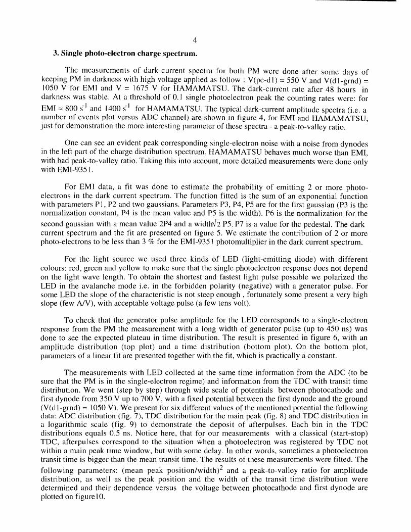
To check that the generator pulse amplitude for the LED corresponds to a single-electron response from the PM the measurement with a long width of generator pulse (up to 450 ns) was done to see the expected plateau in time distribution. The result is presented in figure 6, with an amplitude distribution (top plot) and a time distribution (bottom plot). On the bottom plot, parameters of a linear fit are presented together with the fit, which is practically a constant.
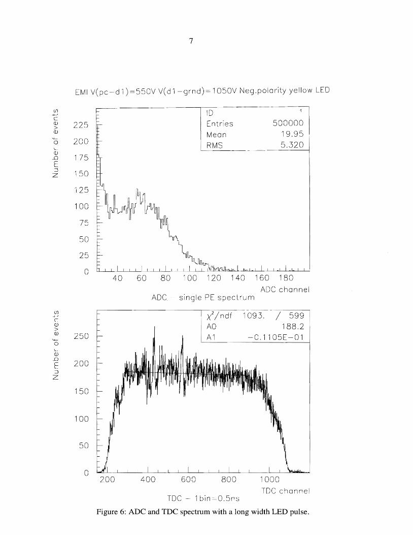
The measurements with LED collected at the same time information from the ADC (to be sure that the PM is in the single-electron regime) and information from the TDC with transit time distribution. We went (step by step) through wide scale of potentials between photocathode and first dynode from 350 V up to 700 V, with a fixed potential between the first dynode and the ground (V (d l-grnd) = 1050 V). We present for six different values of the mentioned potential the following data: ADC distribution (fig. 7), TDC distribution for the main peak (fig. 8) and TDC distribution in a logarithmic scale (fig. 9) to demonstrate the deposit of afterpulses. Each bin in the TDC distributions equals 0.5 ns. Notice here, that for our measurements with a classical (start-stop) TDC, afterpulses correspond to the situation when a photoelectron was registered by TDC not within a nlain peak time window, but with some delay. In other words, sometimes a photoelectron transit time is bigger than the mean transit time. The results of these measurements were fitted. The
following parameters: (mean peak position/width)2 and a peak-to-valley ratio for amplitude distribution, as well as the peak position and the width of the transit time distribution were determined and their dependence versus the voltage between photocathode and first dynode are plotted on figurelO.

5
Dark current spectrum r EMI and HAMAMATSU
OJ 30000> OJ
'-+
o L 25000
E 1 20000
15000
10000
50
o
OJ 16000 > OJ
'-+
0 14000 L
12000E :=J
z
8000
6000
4000
2
0
ADC channel EMI 550V- 1050V
ADC channel HAMAMATSU HV= 1675V
Figure 4 : Typical dark-current amplitude spectra.

6
EMI PM.V(pc d1 )=550V.V(d1-grnd)=11 OOV.Threshold 0.1 pe.
en ........... c Q)
~ 30000 4
o L Q)
.D
E ~ 25000
20000
15000
10000
5000
o
648.7 / 2 12.42
0.7956E-01 0.1953E +05
.91 P5 31.62 P6 359.6 P7 18.93 I
I
\ I \
\ ," \ : I: r
:\
\
\
channel ADC Dark current spectrum
Figure 5 : Fit for EMI dark-current spectrum.
C
7
I V(pc-d 1)=5 V(d 1 -grnd) 1050V Neg.polarity yellow
(f) +--'
Q) 225> Q)
o ' Q)
.D 175 E ::J 150Z
125
100
75
50
25
o
10 Entries
Mean
RMS 5.320
AOC channel AOC single P spectrum
(f) +--' C Q)
> Q) 250
' Q)
E 200 ::J
Z
100
50
o
1
O.1105E-01
TOC channel TOC - 1 bin O.5ns
Figure 6: ADC and TDC spectrum with a long width LED pulse.

8
Ingle PE spectra V(d1 grnd)
Ilndf 71.70 I 531500 Constant 1167. Mean 57.49 Si ma 20.67
1000
500
0 50 100 150
V(pc d1)=350v
x'/ndf SOLO I 78 Constant 8391. Mean 66.478000 Sigma 22.73
6000
4000
2000
0 50 100 150
V(pc-d1)=
x:Indf 62.42 I 63 Constant 1102. Mean 72.79
i Si ma 23.87
1000
500
0 50 100 150
V(pc d1) 600v
1050v. ff.V(pc-d1 ).LED -Neg.polar.
I 53 1110. 64.21 21.811000
500
0 50 100 150
V(pc d1)=450v
Kindt 34.90 I 53 Constant 2177. Mean 70.90
22.672000
1000
0 50 100 150
V(pc d 1 ) 550v
Sigma
2000
1500
1.000
500
0 50 100 150
V(pc-d 1) 700v
I 63 2140. 77.22 25.38
Figure 7: Single-electron amplitude distributions for different photocathode -first dynode potential.

100
9
80
6000
4000
2000
o 410
1bin 0.5ns V(d 1 grnd)= 1 050v. Oiff.V(pc d 1 ).LEO
--.~.-- ---r-'i';-;-/n--:df--=-86::-::-99~.~/--;---:-1-::-16
Constant Mean Si ma
420 430
V(pc-d 1)=350v
3000015000
2000010000
100005000
0 0 410 420 430
V(pc
15000
5000
o
5592. 426.9 2.536 8000
6000
4000
2000
o 410 420
V(pc-d1)
Neg.polar.
i'/ndf 2200. I 10 Constant 7080. Meon 421.1 5i ma 1.685
430
450v
I/ndf 2867. I 12 Canstont 0.2785E+05 Mean 420.3 5i ma 1.619
d1)=525v V(pc d 1)=
i'/ndf 362.2 I 12 I I/ndf 265.2 I 1230000Constant 0.1361E+05 Constant 0.2914E+05
Mean 418.1 Si ma 1.887
20000
10000
o 420 430410
V(pc-d1) 600v V(pc-d1 )=700v
Figure 8 : Transit time distributions for different photocathode-first dynode potential.

10
Toe 1bin=0.5ns V(d 1-grnd)= 1050v. Oiff.V(pc d 1 ).LEO Neg.polar.
ID 210 4 10 4
Entries 500000 Mean 1828. RMS 445.6
10 3 10 3
10 2 10 2
10 10
400 600 800
V(pc d 1) 350v
400
ID 2 Entries 500000 Mean 1866. RMS 426.9
600 800
V(pc-d1) 450v
10
400 600
ID Entries Mean RMS
2 500000
1759. 554.4
800
V(pc-d 1)=525v
400
2 Entries 1000000 Meon 1804. RMS 509.5
600 800
V(pc d1)=550v
10
400 600
ID Entries Mean RMS
800
2 500000
1764. 530.5
10
400 600
ID Entries Meon RMS
800
2 1000000
1769. 549.0 .
V(pc-d1) 600v V(pc-d 1)=700v
Figure 9: Transit time distributions with afterpulses for different photocathode-first dynode potential.
6
• 5.5.... = '0 ~
I:: 5 '33 8 =4.5 '~
~ 4 o .....= :r: 3.5
fZ ~
300
428
426 ~
~
= CQ= 424 .c
..:!.
.5 ~ 422 .... :: fIl 420 CQ= ....'""
.:c 418CQ
~ 416
11
(a)
! ! I
i II I I
I
I
400 500 600 700 800
Voltage [volts]
(c)
I
(b)
2.4
2.2
0 ':C 2r: ;,.. .! 1.8
CQ -j;o>. .s 1.6 ~
CQ ~
~ 1.4
1.2 300 400 500 600 700
Voltage [volts]
(d)
1.8
~ fIl .s 1.6 .b '-'
.c.... 1.4
'i"C
~
~ 1.2 I ....
';; II f=r: !~ I I 0.8
300 400 500 600 700 800 300 400 500 600 700 800
Voltage [volts] Voltage [volts]
Figure 10 : Main parameters of EMI versus the voltage between the photocathode and the first dynode:
a) (mean peak position/width)2 (pedestal subtracted) : this parameter for single photoelectron regime is dominated by the gain coefficient of the first dynode;
b) peak-to-valley ratio; c) main peak position in transit time distribution; d) width of the transit time distribution.
All parameters after V(pc-dl) = 550V change rather slowly, that indicates that the voltage between photocathode and first dynode less than 550 V is not enough to create a proper electric field to collect photoelectrons to the first dynode. In the range 550-700 V one can see a slow rise of the peak-to-valley ratio: by increasing V(pc-dl), we improve the collecting conditions for the photoelectrons. We also see a systematic decrease of the position of the main peak in transit time distribution, due to an increase of the electric field inside of the PM bulb.
4. Transit time distribution.
The main peak in the transit time distribution plot, shows the regular gaussian shape when the voltage between photocathode and first dynode is larger than 500 volts. Using data from plot (d) on figure I 0, we estimated the width of the main peak as 0' = (1.0 ± 0.1) ns.
800

12
5. Multiple photoelectrons spectrum.
Knowing the generator amplitude corresponding to one single photoelectron response (fron1 the measurement with a long width of a generator pulse), we increased the LED generator amplitude and investigated the multiple photon response of the EMI PM. The resulting plot is presented in figure 11 with the fit of an exponential function (to describe a left part of the distribution) and 6 gaussians with qi = Nql and O'i = O'f{N, where N= 1,2, ... 6 (like for the figure 5). Paran1eters PI-P8 on the plot are: P7, P8 correspond to fit of exponential function and PI-P6 are proportional to the probabilities of emitting 1 to 6 photoelectrons. They follow to the Poisson distribution:
xn Pen) = exp(-x) I with x=1.94 n.
EMI Green PD. Start from generator
5000
4000
3000
2000
1000
o
P1 0.3663E+06 P2 0.3605E+06 P3 0.2187E+06 P4 0.1209E+06 P5 0.4394E+05 P6 0.2381 E+05 P7 12.93 P8 -0.5S96E 01
100 200 300 400 500 600
Figure 11 : Multiple photoelectron amplitude distribution.
6. Spectra with a lot of photoelectrons (linearity).
We measured also a response from the EMI PM when the nurnber of photoelectrons is larger than 10, by increasing the amplitude of the LED generator pulse. For each measurement we had a

13
regular gaussian amplitude distribution. Fitting it we obtained a mean peak position and a width( 0').
After that a parameter - (mean peak position/width)2 was calculated, which corresponds to the number of photoelectrons emitted from the photocathode. The result of these measurements is shown on figure 12 as the number of photoelectrons vs the mean peak position (ADC channel). One can see a satisfactory linearity of the PM, when the number of photoelectrons changes from 10 up to 200. So we checked the possibility to use the EMI PM both in the single photoelectron regime and with a big amount of light.
250
200
~ ~ 150 ~
<= ~
,.Q100e
::s:z 50
0
0 200 400 600 800 1000
ADC channel (0.5 pC/channel)
Figure 12 : Amplitude linearity. 7. Afterpulses.
Some additional measurements were done to understand what parameters are more important for afterpulses. For each measurenlent two values were calculated: N . - is the number of events
mam
corresponding the main peak in the time distribution (±5 0' from the main peak position) and Naftp
is the number of events within a time window 100 ns after the nlain time window. The ratio
N . /N ft was chosen as a parameter to describe the deposit of the afterpulses. These ratios were mam a p obtained for:
1) different voltages between the photocathode and first dynode (V(pc-d1)) at fixed voltage between first dynode and ground (V(dl-grnd)=1050V) in the single photoelectron regime (figure 13 - a); 2) different V(dl-grnd) at fixed V(pc-dl) =550V, the threshold being changed to keep it at 0.1 times the single photoelectron peak for different V(dl-grnd):
(figure 13 - b ) for the single photoelectron regime; (figure 13 - c) for measurements with a mean number of photoelectrons about 10;
3) different thresholds at fixed V (d 1-grnd)= 11 OOV and V (pc-d 1 )=5 50V in the single photoelectron reginle:
(figure 13 - d) as a function of the ratio of a threshold to peak position (pedestal was subtracted).
For fig.13-a and 13-b we added the information about measured charge (from corresponding amplitude distributions) to demonstrate how to renormalize the anode signal when V(dl-grnd) and V(pc-d1) are changing.

14
plot "bl!plot "a"
6
.:I. C# ill Cl.5 c'; 8 0 ... 4 r.fJ ill r.fJ
'S CI.
"" ~ 3 ~ ,..... ~ '0 .:: 2 c# ~
:4 cc Q,j Q"
c 0.8 .; S S 0.6 til Q,j
.!!l :I Q"
t 0.4 c:: < 1"""1
~ ""-10.2 .S .... cc=:
I I I I
. x Measured charge(ADC channel) x Ratio[% J:Afterpulses to main peak x
x x
x
x
X
I ! ! I
0 Xx Measured charge(ADC channel) . Ratio[%J:Afterpulses to Main Peak
x
x
x
x
X
80'D
.:I. tr)'-' ~ 4.5 70~ tr)'Z Q. c c c c c
4 6O.cCIt
uo.c C# ';
V) u ~ UU 0
Q 50 Q... 3.5 < r.fJv) ~
<&,..." ill illcu r.fJ CI)CI) 'S 3 40 ;"" CI.c# .co.c uill<& u ""
ct: 30 "0"0 < 2.5 cuill ,..... V) "" ::"" ('!") ~ ~ 20 :ell illill :s 2
... ~ o~ c# ('!") ~ 1.5 10
V) ('l 0
300 400 500 600 700 800 900 950 1000 1050 1100 1150 1200 1250 V(pc-dl) (volts) V(dl'grnd) (volts)
plot "e" plot lid"
I I I I I I 3.7
Mean value of Npe=9.3±OJ .:i. C\I cu CI.
-c'; 3.2 8 0...
- r.fJ ill r.fJ
"3 CI.
2.7
""ill
- I ct:< 2.2 ,..... ~ :§'
I ... C\I 1.7 ~
I I I I I
I I
! I I I I1.20 I I I I I I
900 950 1000 1050 1100 1150 1200 1250 0.1 0.2 0.3 0.4 0.5 0.6
V(dl.grnd) (volts) Threshold in Ispe
Figure 13 : Afterpulses versus different parameters.
The results of these measurements permit us to make the following conclusions: 1. afterpulses decrease with increasing of number of photoelectrons emitted from the
photocathode, due to the decrease of the probability to miss a photoelectron (remind here again that we used classical TDC in our measurements);
2. afterpulses do not change dramatically when changing V(pc-d1) and V(dl-grnd) from 350V up to 700 V and from 950 V up to 1200 V respectively;
3. even in the single photoelectron regime, afterpulses practically do not depend on the output signal threshold, at least when a threshold changes from 0.1 up to 0.6 of the mean value of single photoelectron peak position;
4. afterpulses are mainly located within a time window of 25 ns, which is itself delayed after the main peak about 45 ns (see figure 9).

15
8. Decay time of the scintillators.
With the EMI and another PM, HP 2020, the time parameters of scintillators (Od-free and
Od-loaded) were measured. A snlall quartz box with dimensions 8 x 8 x 50 mnl' was filled with
scintillator. On the top of the box a 207Bi source was placed. The box had optical contact with the HP 2020 . The distance between the box and the EMI-PM was chosen to obtain the single electron regime for the EMI. The amplitude distributions were measured for both PM. Signals from HP 2020 gave the trigger for EMI amplitude and time analyses. Time distributions of both PM were measured with a LED to demonstrate that time parameters of PM are much faster than those of the scintillator. Figure 14 shows the corresponding ADC and TDC spectra for both PM.
Single PE time distribution for EMI and H 020 with yellow
Indf 57.82 I 68 5000 · x/ndf 212.6 I 63 Constant 660.6 Constant 3954.700
600 4000
500 3000
400
300 2000
200 1000
100
o o 20 40 60 80
ADC-HP2020 PM- 1 sing pe
50 100 150
ADC-EMI 1 single pe
2000 2000
o 230 240 250 260
TOC-EMI PM 1 bin O.5ns TOC- P2020 PM 1 bin 0.5ns
Figure 14: ADC and TDC distributions of both EMI-9351 and HP 2020.
I Mean 22.82 Si ma 25.50
-I/ndf 657.4 I 10 Constant O.1035E+05 Mean 242.5 Si ma 1.391
14000 10000
12000
8000 10000
6000 8000
60004000
4000
-Ilndf 1267. I 10 Constant O.1332E+05 Mean 232.4 Si ma 1.700
16
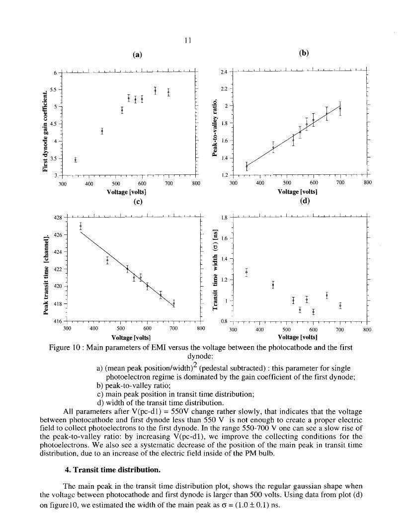
In figure 15 and 16 we present the results of time-constant measurements for both scintillators (gadolinium-free and gadolinium-loaded).
100 200 300 400 500 600
tdc 1bin= 1ns
Figure 15: Time-constant measurements for gadolinium-free scintillator.

17
(f) +-' X
2/ ndf 833.9 / 556 c
ill P1 8.452> ill
'+-
10 40 L
ill ..D
E :::J z
10 3
10
200 300 400 500 600
tdc 1bin=1ns
I
", I '1 I
I
P6 P7 P8 P9 P10
-0.4141E 01 16.80
-0.2469 1 .8 68.83 3.9 3.734
-0.1027E 01 2.782
T1=4.0 ns
T2=24.2 ns
T3=96.0 ns
100
Figure 16 : Time-constant measurements for gadolinium-loaded scintillator.

18
A fit with three exponentials (to describe time constants of a scintillator) and a gaussian (for
afterpulses) was done for both figures. The results of the fit are (they are also presented on figures):
• For the gadolinium-free scintillator, the time constants are:
1:1 = (7.3 ± 0.4) ns ; 1:2 = (31.7 ± 1.6) ns 1:3 = (93.6± 4.7) ns
The corresponding probabilities are: y 1 = (70 ± 4)% Y2 = (28 ± 1)%. y 3 = (2 ± 0.1)%
• For the gadolinium-loaded scintillator, the time constants are: 1:1 = (4.0± 0.2) ns ; 1:2 = (24.2± 1.2) ns . 1:3 = (96.0 ± 4.8) ns
The corresponding probabilities are: Yl =(72±4)% Y2 =(26± 1)%.
Conclusions
The tests performed on EMI showed us that this tube suits well the purposes of CHOOZ experin1ent, mainly due to :
a) low dark curent noise rate;
b) good single-electron response;
c) narrow single-photoelectron transit time distribution;
d) good linearity up to 2 V for anode output signals.
Note also that the glass of the tube has a low contamination of radioactive materials. This last point is very important for a low background experiment like CHOOZ.
Acknowledgement
We thank the Thorn EMI and HAMAMA TSU societies for their help and for fruitful discussions. We are waiting for a new PM from HAMAMATSU (R5912), which must have much better peak-to-valley ratio than R4558. We thank also M.Sene for his help and advice.
I Proposal to search for neutrino vacuum oscillations to Llm2 =10-3 eV2 using a 1 km baseline reactor neutrino experiment NIM .....
2 See reference 1.
3 See reference 1.
4 Performances of large cathode area phototube for underground physics applications. G. Rannucci, R. Cavalletti, P. Inzani and S. Schoner. INFN/AE-92/09.
5 Characterisation and magnetic shielding of the large cathode area PMT's used for the light detection system of the prototype of the solar neutrino experiment Borexino. G. Rannucci et al. NIM A 337 (1993) 211-220.
6 Data sheet from Thorn EMI.RIP 069 Voltage Divider Design.


