Microfabricated Amorphous Silicon Nanopillars on an
Ultrasmooth 500-nm-thick Titanium Adhesion Layer
by Collin R. Becker, Kenneth E. Strawhecker, Jonathan P. Ligda,
and Cynthia A. Lundgren
ARL-TR-6209 September 2012
Approved for public release; distribution unlimited.

NOTICES
Disclaimers
The findings in this report are not to be construed as an official Department of the Army position
unless so designated by other authorized documents.
Citation of manufacturer’s or trade names does not constitute an official endorsement or
approval of the use thereof.
Destroy this report when it is no longer needed. Do not return it to the originator.
Army Research Laboratory Adelphi, MD 20783-1197
ARL-TR-6209 September 2012
Microfabricated Amorphous Silicon Nanopillars on an
Ultrasmooth 500-nm-thick Titanium Adhesion Layer
Collin R. Becker, Kenneth E. Strawhecker, Jonathan P. Ligda,
and Cynthia A. Lundgren Sensors and Electron Devices Directorate, ARL
Approved for public release; distribution unlimited.
ii
REPORT DOCUMENTATION PAGE Form Approved OMB No. 0704-0188
Public reporting burden for this collection of information is estimated to average 1 hour per response, including the time for reviewing instructions, searching existing data sources, gathering and maintaining the
data needed, and completing and reviewing the collection information. Send comments regarding this burden estimate or any other aspect of this collection of information, including suggestions for reducing the
burden, to Department of Defense, Washington Headquarters Services, Directorate for Information Operations and Reports (0704-0188), 1215 Jefferson Davis Highway, Suite 1204, Arlington, VA 22202-4302.
Respondents should be aware that notwithstanding any other provision of law, no person shall be subject to any penalty for failing to comply with a collection of information if it does not display a currently valid
OMB control number.
PLEASE DO NOT RETURN YOUR FORM TO THE ABOVE ADDRESS.
1. REPORT DATE (DD-MM-YYYY)
September 2012
2. REPORT TYPE
Final
3. DATES COVERED (From - To)
4. TITLE AND SUBTITLE
Microfabricated Amorphous Silicon Nanopillars on an Ultrasmooth 500-nm-thick
Titanium Adhesion Layer
5a. CONTRACT NUMBER
5b. GRANT NUMBER
5c. PROGRAM ELEMENT NUMBER
6. AUTHOR(S)
Collin R. Becker, Kenneth E. Strawhecker, Jonathan P. Ligda, and
Cynthia A. Lundgren
5d. PROJECT NUMBER
5e. TASK NUMBER
5f. WORK UNIT NUMBER
7. PERFORMING ORGANIZATION NAME(S) AND ADDRESS(ES)
U.S. Army Research Laboratory
ATTN: RDRL-SED-C
2800 Powder Mill Road
Adelphi, MD 20783-1197
8. PERFORMING ORGANIZATION REPORT NUMBER
ARL-TR-6209
9. SPONSORING/MONITORING AGENCY NAME(S) AND ADDRESS(ES)
10. SPONSOR/MONITOR’S ACRONYM(S)
11. SPONSOR/MONITOR'S REPORT NUMBER(S)
12. DISTRIBUTION/AVAILABILITY STATEMENT
Approved for public release; distribution unlimited.
13. SUPPLEMENTARY NOTES
14. ABSTRACT
Amorphous silicon (Si) nanopillars are fabricated using electron beam lithography for a liftoff process. The nanopillars are
fabricated on an ultrasmooth, 6.5-nm root mean square (RMS) roughness, 500-nm-thick titanium (Ti) layer using electron beam
evaporation. Pillars ranging from 100‒1000 nm in diameter and approximately 200 nm in height are fabricated. Atomic force
microscopy (AFM) and scanning electron microscope (SEM) images, including those collected by focused ion beam (FIB)
milling, are presented to analyze the shape of the pillars and roughness of the Ti film. The smoother the Ti/Si interface, the
more robust the adhesion of Si to Ti becomes.
15. SUBJECT TERMS
Silicon, electron beam lithography, nanopillar, nanowire
16. SECURITY CLASSIFICATION OF: 17. LIMITATION OF ABSTRACT
UU
18. NUMBER OF PAGES
24
19a. NAME OF RESPONSIBLE PERSON
Collin R. Becker a. REPORT
Unclassified
b. ABSTRACT
Unclassified
c. THIS PAGE
Unclassified
19b. TELEPHONE NUMBER (Include area code)
(301) 394-0476
Standard Form 298 (Rev. 8/98)
Prescribed by ANSI Std. Z39.18
iii
Contents
List of Figures iv
List of Tables iv
Acknowledgments v
1. Introduction 1
2. Experimental 1
2.1 Titanium Deposition ........................................................................................................1
2.2 Nanopattern Fabrication ..................................................................................................1
2.3 Silicon Deposition and Liftoff .........................................................................................2
2.4 Characterization...............................................................................................................2
3. Results and Discussion 2
4. Conclusion 9
5. References 10
Appendix A. SEM Analysis of Sputtered Ti Film 11
Appendix B. SEM Analysis of Pillar Cross Section 13
List of Symbols, Abbreviations, and Acronyms 15
Distribution List 16

iv
List of Figures
Figure 1. The 500-nm-thick Ti films deposited at (a) 0.2 nm/s and (b) 0.05 nm/s. ........................3
Figure 2. (a) Si nanopillars deposited on 500-nm-thick “rough” Ti, 0.2 nm/s deposition rate; (b) Si nanopillars deposited on 500-nm-thick “smooth” Ti, 0.05 nm/s deposition rate; (c) 100-nm-diameter pillar on the “rough” Ti; and (d) 100-nm pillar on the “smooth” Ti. ......4
Figure 3. AFM images of Si nanopillars (a) pre- and (b) post-oxygen plasma ash treatment. .......5
Figure 4. AFM images of 500 nm thick Ti deposited at (a) 0.2 nm/s and (b) 0.05 nm/s. ..............7
Figure 5. AFM images of Si pillars on “rough” Ti with poor adhesion on (a) the initial scan, (b) the second scan, and (c) is an SEM image showing a large region of missing pillars as a result of AFM interaction. .......................................................................................................7
Figure 6. (a) An SEM image at oblique angle of the 1000-nm pillar, (b) an SEM image of pillars analyzed with FIB, and (c) a close up SEM image after FIB milling of the 1000-nm pillar. ...........................................................................................................................8
Figure 7. Raman spectrum of Si nanopillars. ..................................................................................8
Figure A-1. SEM images with (a) 1000- and (b) 500-nm scale bars of 500-nm-thick Ti films deposited by DC magnetron sputtering....................................................................................11
Figure B-1. SEM cross section of a 300-nm- diameter Si nanopillar on a Ti film deposited at 0.05 nm/s on a Si wafer............................................................................................................13
List of Tables
Table 1. Average height of Si nanopillars pre oxygen plasma treatment. .....................................5
Table 2. Average height of Si nanopillars post oxygen plasma treatment. ....................................6
Table 3. Comparison of designed pillar diameter with diameters measured by AFM and SEM. ..........................................................................................................................................6
v
Acknowledgments
We would like to thank Dr. Madhu Roy and Dr. Rob Burke for discussion with electron beam
lithography and acknowledge the U.S. Army Research Laboratory for funding.

vi
INTENTIONALLY LEFT BLANK.
1
1. Introduction
Silicon (Si) is viewed as one of the most promising materials to improve the energy capacity of
lithium-ion batteries. Work by many groups demonstrates that nanoscale Si offers dramatic
improvements in cycle life compared to bulk-scale Si (1, 2). The reasons for this improvement
have been explored from many angles, but more work is needed to clarify the precise reasons for
this improvement. Specifically, studies of Si nanostructures anchored to a metal current
collector such as copper or titanium (Ti) need further refinement and study to explore volume
change and interface effects from the substrate.
Here, methods to produce precision amorphous Si nanopillars on a Ti substrate using
microfabrication techniques including electron beam lithography and liftoff methods are
described. The method is somewhat unusual in that the adhesion layer, Ti, is exposed to air prior
to Si deposition and is quite thick, 500 nm. A similar approach has been used by other research
groups (3). Presented here, using atomic force microscopy (AFM), Raman spectroscopy,
focused ion beam (FIB), and scanning electron microscopy (SEM), is a detailed investigation of
the size and shape, phase (amorphous or crystalline), and Si/Ti interface of the pillars.
2. Experimental
2.1 Titanium Deposition
We used Si wafers with a resistivity of 1–20 ohm-cm or 0.01–0.02 ohm-cm (the resistivity is
chosen for particular end applications). Ti of 99.995% purity was deposited using an Evatek
BAK 641 electron beam evaporator at either 0.2 or 0.05 nm/s operating at 1.9 x 10⁻⁶
mbar initial
background pressure. The thickness was monitored by quartz crystal.
2.2 Nanopattern Fabrication
After Ti deposition, the wafers were pretreated with 10 ml of liquid hexamethyldisilazane
(HMDS) to promote adhesion by photoresist. The HMDS was removed by rotating the wafer at
2000 rpm for 40 s and then heating on a hot plate for 60 s at 110 °C. Next, approximately 5 ml
of positive electron beam photoresist (ZEP 520A) was deposited on the wafer. The wafer was
spun at 2000 rpm for 60 s and then baked on a hot plate for 180 s at 175 °C. The thickness of the
photoresist was 389 nm as confirmed by stylus profilometry (Tencor).
The desired nanopillar pattern was transferred to the resist using electron-beam lithography
(Vistec EBPG5000+ES). The pattern was generated using a beam at a 100-kV, 10-pA current

2
and with a 300-µCcm–2
dose. Additionally, square Si pads used as guides when locating pillars
for images were patterned using a 50-pA beam and 300-µCcm–2
dose. The write time for four
samples per wafer composed of 1x10⁶ pillars/sample was approximately 50 min. The resist was
then developed for 90 s at 21 °C in xylenes and then was rinsed for 30 s in methyl isobutyl
ketone (MIBK).
2.3 Silicon Deposition and Liftoff
Prior to deposition, a 5-min descum operation using an Anatech barrel asher was performed.
The power was tuned to 200 W and the gas flow was 400 sccm. After this descum, the resist
thickness was 368 nm. Again using electron beam evaporation (Evatek BAK 641), Si (99.999%)
was deposited at a rate of 0.2 nm/s. The thickness was monitored by quartz crystal. For liftoff,
the wafer was immersed in acetone until most of the photoresist/Si had been removed. The
wafers were then rinsed with acetone, methanol, isopropyl alcohol (IPA), deionized (DI) water,
and transferred without drying to a Microposit 1165 photoresist remover and held at 80 °C for
2 h. The wafers were then rinsed in DI water and dried with flowing nitrogen. As a final step, a
Metroline oxygen plasma etcher operating at 400 W and 500 sccm was used to help remove
photoresist debris.
2.4 Characterization
AFM (either a Veeco Dimension 3100 or Agilent 5500) was used to measure heights and
diameters of the pillars and roughness of the substrate. SEM (FEI environmental SEM) was used
to investigate morphology of the pillars and a FIB microscope (FEI) was used to analyze the
interface of the pillars. A Renishaw Raman InVia system with a 514 nm wavelength laser was
used for Si phase analysis.
3. Results and Discussion
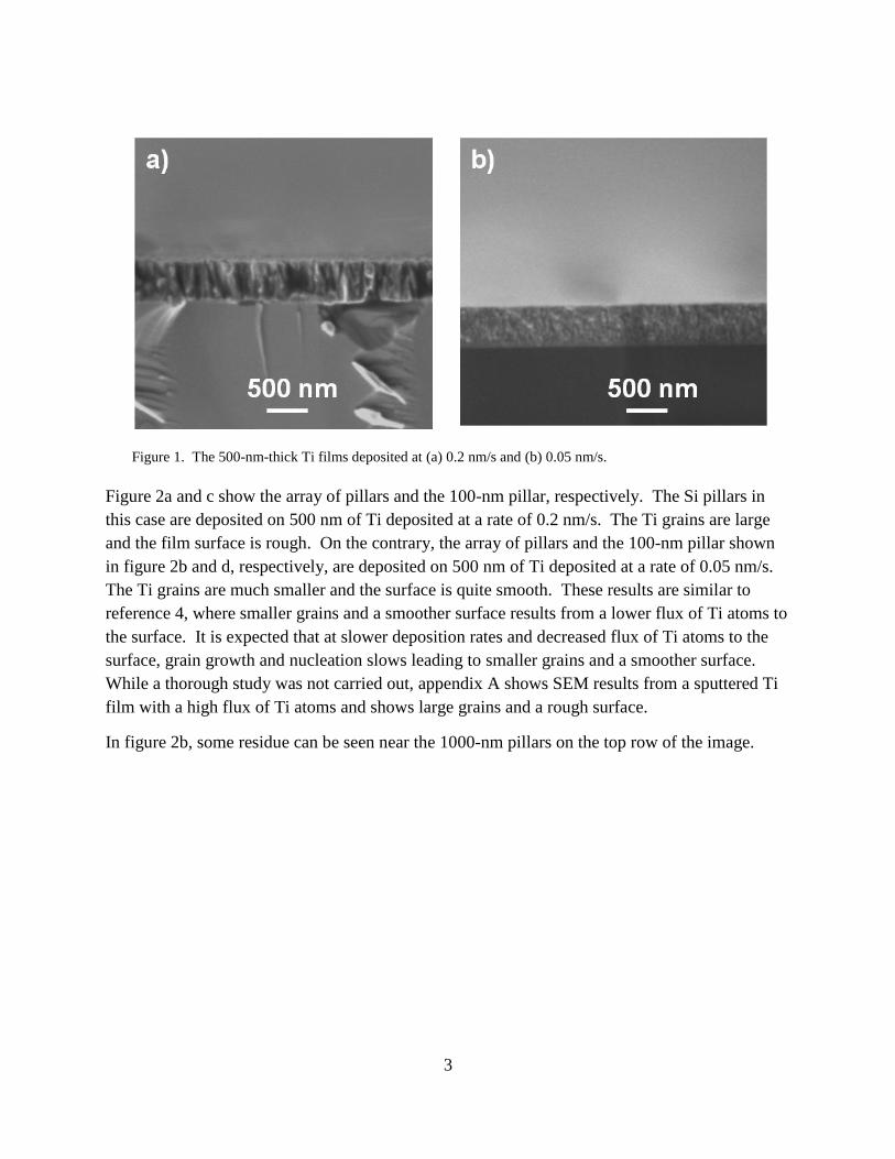
Figure 1a and b show SEM cross sections of the 0.2 and 0.05 nm/s Ti films on Si, respectively.
The films are measured to be within ±20 nm of the 500-nm target thickness. The 0.2-nm/s film
shows large columnar grains while the 0.05-nm/s film has a microstructure with smaller grains.
3
Figure 1. The 500-nm-thick Ti films deposited at (a) 0.2 nm/s and (b) 0.05 nm/s.
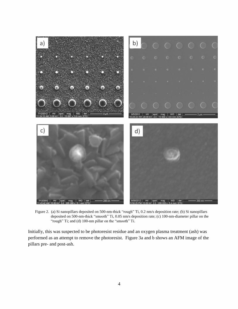
Figure 2a and c show the array of pillars and the 100-nm pillar, respectively. The Si pillars in
this case are deposited on 500 nm of Ti deposited at a rate of 0.2 nm/s. The Ti grains are large
and the film surface is rough. On the contrary, the array of pillars and the 100-nm pillar shown
in figure 2b and d, respectively, are deposited on 500 nm of Ti deposited at a rate of 0.05 nm/s.
The Ti grains are much smaller and the surface is quite smooth. These results are similar to
reference 4, where smaller grains and a smoother surface results from a lower flux of Ti atoms to
the surface. It is expected that at slower deposition rates and decreased flux of Ti atoms to the
surface, grain growth and nucleation slows leading to smaller grains and a smoother surface.
While a thorough study was not carried out, appendix A shows SEM results from a sputtered Ti
film with a high flux of Ti atoms and shows large grains and a rough surface.
In figure 2b, some residue can be seen near the 1000-nm pillars on the top row of the image.
4
Figure 2. (a) Si nanopillars deposited on 500-nm-thick “rough” Ti, 0.2 nm/s deposition rate; (b) Si nanopillars
deposited on 500-nm-thick “smooth” Ti, 0.05 nm/s deposition rate; (c) 100-nm-diameter pillar on the
“rough” Ti; and (d) 100-nm pillar on the “smooth” Ti.
Initially, this was suspected to be photoresist residue and an oxygen plasma treatment (ash) was
performed as an attempt to remove the photoresist. Figure 3a and b shows an AFM image of the
pillars pre- and post-ash.

5
Figure 3. AFM images of Si nanopillars (a) pre- and (b) post-oxygen plasma ash treatment.
The ash treatment does not appear to degrade the substrate or pillars since the heights remain
similar. However, the residue is still present and the exact cause and composition of this residue
is being investigated. It was found that with ultrasonic treatment during the lift-off process, the
residue was not as prevalent; however, the ultrasonic treatment had a tendency to delaminate
some pillars, as seen in figure 1a, and is not a preferred technique. This result seems to indicate
the residue is redeposition of either photoresist or Si during the liftoff process.
Tables 1 and 2 present the heights and diameters of the pillars pre- and post-ash. The averages
are computed for 5–7 pillars and do not appear to be drastically different after the ash. Some of
the difference arises from the inability to examine the exact same pillars after the ash or from
slight tip degradation during scanning.
Table 1. Average height of Si nanopillars pre
oxygen plasma treatment.
Pre Oxygen Plasma Treatment
Designed Pillar Diameter (nm)
Average Height (nm)
1000 231 +/- 2
500 240 +/- 2
300 255 +/- 10
200 255 +/- 6
100 117 +/- 6

6
Table 2. Average height of Si nanopillars post
oxygen plasma treatment.
Post Oxygen Plasma Treatment
Designed Pillar Diameter (nm)
Average Height (nm)
1000 219 +/- 1
500 229 +/- 2
300 249 +/- 2
200 251 +/- 5
100 139 +/- 13
Table 3 indicates the diameter of the pillars on the smooth Ti substrate. AFM is known to be
extremely accurate in the Z-direction, but can have a tip broadening effect in the x,y direction.
Here it is shown that the AFM overestimates the diameter of the pillar since the pillar diameter is
larger at full width at half maximum (FWHM) than even SEM shows for the base of the pillar.
AFM can give the approximate slope of the sidewalls of the pillars though, and it is found to be
around 60°. This agrees closely to the SEM image shown in appendix B, which has a measured
angle near 51°. In the future, a more vertical sidewall is likely to be desired, which may be
found by heat treatment of the photoresist (5) or perhaps working with poly(methyl
methacrylate) (PMMA) rather than ZEP electron beam photoresists.
Table 3. Comparison of designed pillar diameter with diameters measured
by AFM and SEM.
Designed Pillar Diameter (nm)
AFM Actual Diameter,
FWHM (nm)
SEM Actual Diameter,
Base (nm)
1000 1085 +/- 15 1060 +/- 32
500 569 +/- 16 531 +/- 18
300 387 +/- 8 363 +/- 12
200 258 +/- 20 261+/- 6
100 234 +/- 21 153 +/- 19
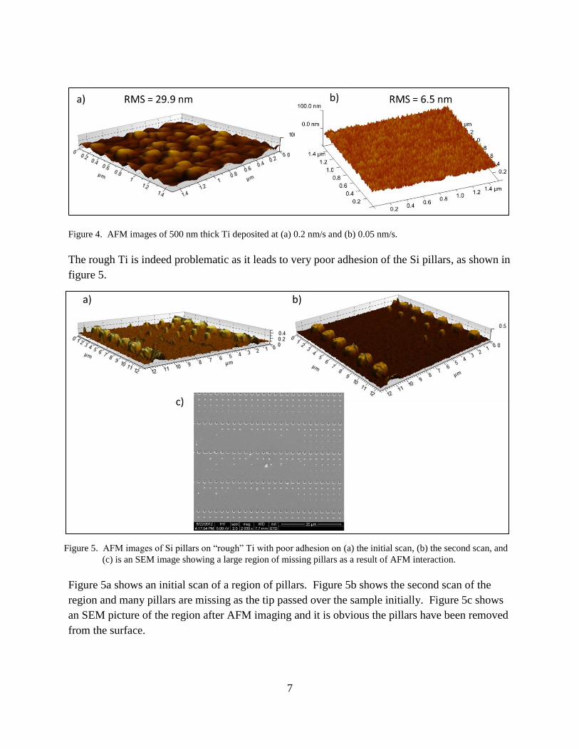
Figure 4 shows AFM images of the Ti substrate of the rough (0.2 nm/s) and smooth (0.05 nm/s)
Ti in figure 4a and b, respectively. The root mean square (RMS) of the rough Ti is 29.9 nm and
the RMS of the smooth Ti is 6.5 nm. Additionally the grains are much smaller in the smooth Ti.
Figure 4a and b are tilted at a slightly different angle to best show the grain morphology, but the
reader should note that both are from a 1.5x1.5 μm area so the grains are indeed considerably
larger for the rough Ti.
7
Figure 4. AFM images of 500 nm thick Ti deposited at (a) 0.2 nm/s and (b) 0.05 nm/s.
The rough Ti is indeed problematic as it leads to very poor adhesion of the Si pillars, as shown in
figure 5.
Figure 5. AFM images of Si pillars on “rough” Ti with poor adhesion on (a) the initial scan, (b) the second scan, and
(c) is an SEM image showing a large region of missing pillars as a result of AFM interaction.
Figure 5a shows an initial scan of a region of pillars. Figure 5b shows the second scan of the
region and many pillars are missing as the tip passed over the sample initially. Figure 5c shows
an SEM picture of the region after AFM imaging and it is obvious the pillars have been removed
from the surface.

8
FIB milling of the samples was carried out to observe the interface of the Ti and Si for the
0.05-nm/s Ti. Figure 6a shows the as-fabricated 1000-nm-diameter pillar, figure 6b shows the
pillars where FIB was used, and figure 6c shows the cross section of the 1000-nm pillar.
Figure 6. (a) An SEM image at oblique angle of the 1000-nm pillar, (b) an SEM image of pillars analyzed with FIB,
and (c) a close up SEM image after FIB milling of the 1000-nm pillar.
A platinum (Pt) mask is deposited in the FIB to reduce damage caused by milling. The Si/Ti
interface is observed to be uniform and smooth without gaps. The Si is also seen to be smooth
and dense.
Lastly, to confirm the pillars are amorphous, Raman spectroscopy with a 514-nm laser was used.
Figure 7 shows a Raman spectrum from the Si pillars and the peak centered near 480 cm–1
indicates the pillars are amorphous Si (6).
Figure 7. Raman spectrum of Si nanopillars.

9
4. Conclusion
Amorphous Si nanopillars are fabricated with a lift-off method using electron beam lithography.
The pillars are deposited by electron beam evaporation on top of a Ti film. It is imperative that a
smooth Ti film is grown for this method to yield Si pillars with good adhesion to the Ti. Using a
slow deposition rate (0.05 nm/s) of Ti can achieve smooth (6.5 nm RMS) films that are 500 nm
thick.

10
5. References
1. Chan, C. K., et al. High-performance Lithium Battery Anodes using Silicon Nanowires.
Nature Nanotechnology 2008, 3 (1), 31–35.
2. Szczech, J. R.; Jin, S. Nanostructured Silicon for High Capacity Lithium Battery Anodes.
Energy & Environmental Science 2011, 4 (1), 56–72.
3. Soni, S. K., et al. Stress Mitigation During the Lithiation of Patterned Amorphous Si
Islands. Journal of the Electrochemical Society 2012, 159 (1), A38–A43.
4. Cai, K. Y., et al. Surface Structure and Composition of Flat Titanium Thin Flms as a
Function of Film Thickness and Evaporation Rate. Applied Surface Science 2005, 250 (1–
4), 252–267.
5. Meyer, D. J., et al. 40 nm T-Gate Process Devlopment Using ZEP Reflow. in CS MANTECH
Conference, Boston, 2012.
6. Brodsky, M. H.; Cardona, M.; Cuomo, J. J. Infrared and Raman-spectra of Silicon-hydrogen
Bonds in Amorphous Silicon Prepared by Glow-discharge and Sputtering. Physical Review
B 1977, 16 (8), 3556–3571.

11
Appendix A. SEM Analysis of Sputtered Ti Film
Ti films were also obtained by sputtering using a CLC 200 Unaxis Clusterline DC magnetron
Sputter Tool operating at 400 W, 5x10⁻³
mbar, and 40 °C. SEM images in figure A-1 show very
large grain sizes similar to the films deposited at 0.2 nm/s in the Evatek evaporator system.
Figure A-1. SEM images with (a) 1000- and (b) 500-nm scale bars of 500-nm-thick Ti films
deposited by DC magnetron sputtering.

12
INTENTIONALLY LEFT BLANK.
13
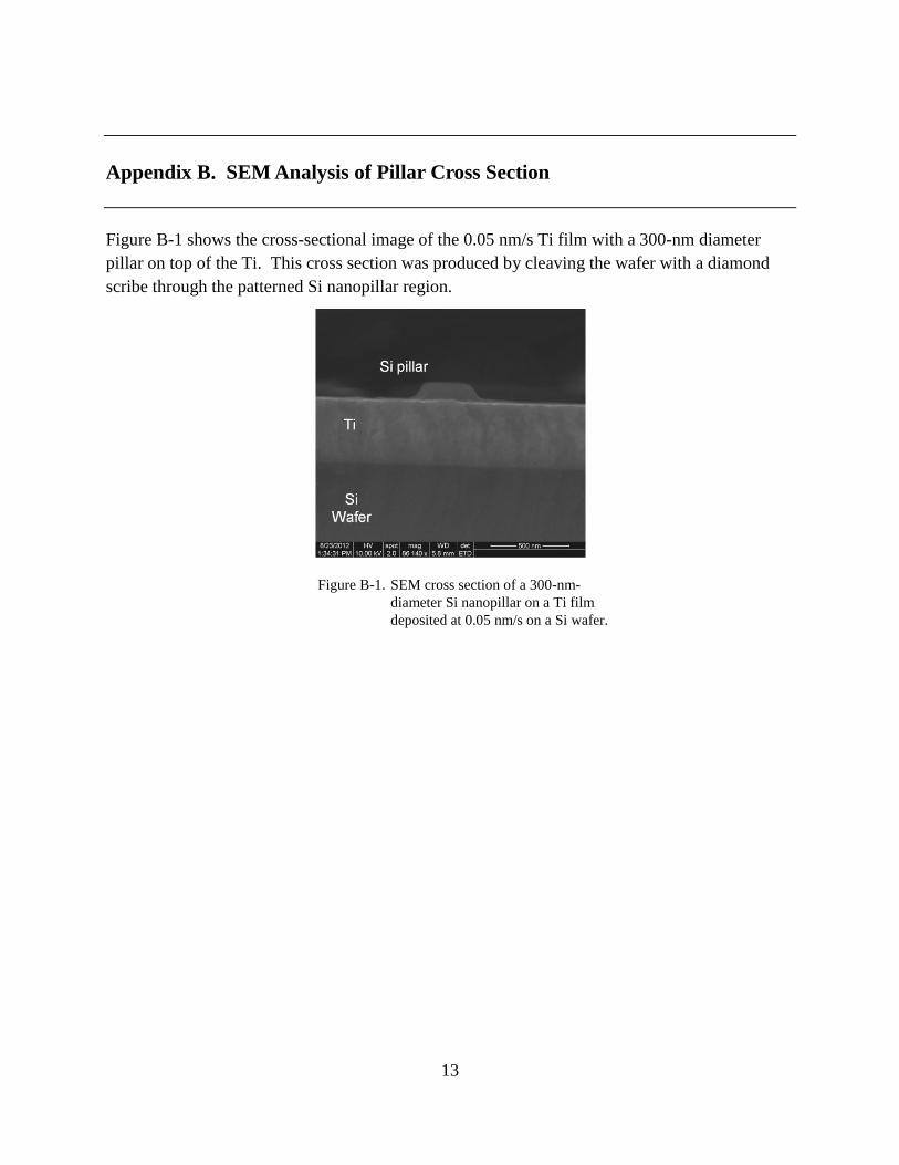
Appendix B. SEM Analysis of Pillar Cross Section
Figure B-1 shows the cross-sectional image of the 0.05 nm/s Ti film with a 300-nm diameter
pillar on top of the Ti. This cross section was produced by cleaving the wafer with a diamond
scribe through the patterned Si nanopillar region.
Figure B-1. SEM cross section of a 300-nm-
diameter Si nanopillar on a Ti film
deposited at 0.05 nm/s on a Si wafer.

14
INTENTIONALLY LEFT BLANK.
15
List of Symbols, Abbreviations, and Acronyms
AFM atomic force microscopy
DI deionized
FIB focused ion beam
FWHM full width at half maximum
HMDS hexamethyldisilazane
IPA isopropyl alcohol
MIBK methyl isobutyl ketone
PMMA poly(methyl methacrylate)
Pt platinum
RMS root mean square
SEM scanning electron microscopy
Si silicon
Ti titanium
16
1 DEFENSE TECHNICAL
(PDF INFORMATION CTR
only) DTIC OCA
8725 JOHN J KINGMAN RD
STE 0944
FORT BELVOIR VA 22060-6218
1 DIRECTOR
US ARMY RESEARCH LAB
IMAL HRA
2800 POWDER MILL RD
ADELPHI MD 20783-1197
1 DIRECTOR
US ARMY RESEARCH LAB
RDRL CIO LL
2800 POWDER MILL RD
ADELPHI MD 20783-1197
1 DIRECTOR
US ARMY RESEARCH LAB
RDRL CIO LT
2800 POWDER MILL RD
ADELPHI MD 20783-1197
5 US ARMY RSRCH LAB
RDRL SED C C LUNDGREN
RDRL SED C C BECKER
RDRL SEG M ROY
RDRL SEG N STRNAD
RDRL SEG W BENARD
ADELPHI MD 20783-1197
2 US ARMY RSRCH LAB
KEN STRAWHECKER
4600 DEER CREEK LOOP, L118
ABERDEEN PROVING GROUND, MD 21005-5069


