Download - MURI Plans
1
MURI PlansMURI Plans
S. E. Thompson March 27, 2005
2
TI Fellows Forum
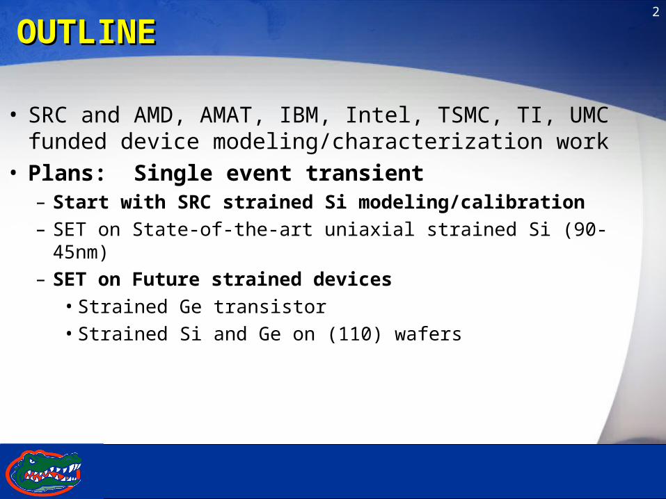
OUTLINEOUTLINE
• SRC and AMD, AMAT, IBM, Intel, TSMC, TI, UMC funded device modeling/characterization work
• Plans: Single event transient– Start with SRC strained Si modeling/calibration– SET on State-of-the-art uniaxial strained Si (90-45nm)– SET on Future strained devices
• Strained Ge transistor• Strained Si and Ge on (110) wafers
3
TI Fellows Forum
1-2.5GPa stress film
Post salicide
Si1-xGex
45nm
Si1-xGex
Removable film pre-anneal
Nitride
Gate Gatestress stressa-Si a-Si
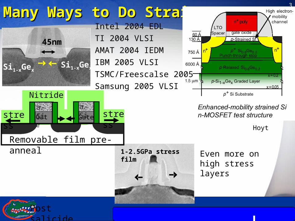
Many Ways to Do StrainMany Ways to Do Strain
Even more on high stress layers
Intel 2004 EDL
TI 2004 VLSI
AMAT 2004 IEDM
IBM 2005 VLSI
TSMC/Freescalse 2005
Samsung 2005 VLSI
Hoyt
4
TI Fellows Forum
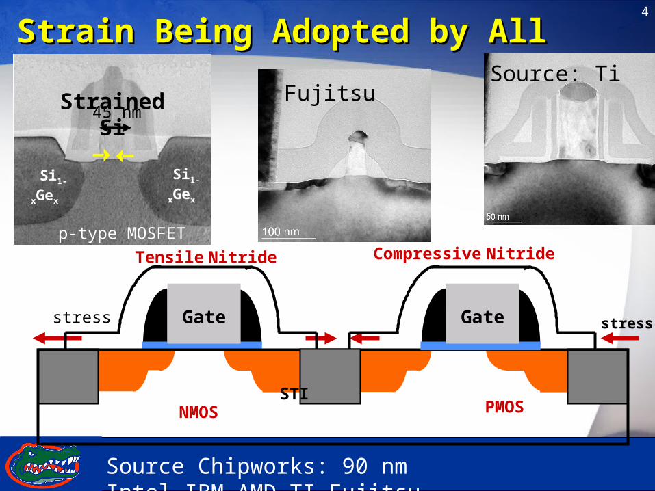
Strain Being Adopted by AllStrain Being Adopted by All
Si1-xGex
p-type MOSFET
Si1-xGex
Strained Si
45 nm
stress stress
NMOS PMOS
Gate
STI
Tensile Nitride Compressive Nitride
Gate
FujitsuSource: Ti
Source Chipworks: 90 nm Intel,IBM,AMD,TI,Fujitsu
5
TI Fellows Forum
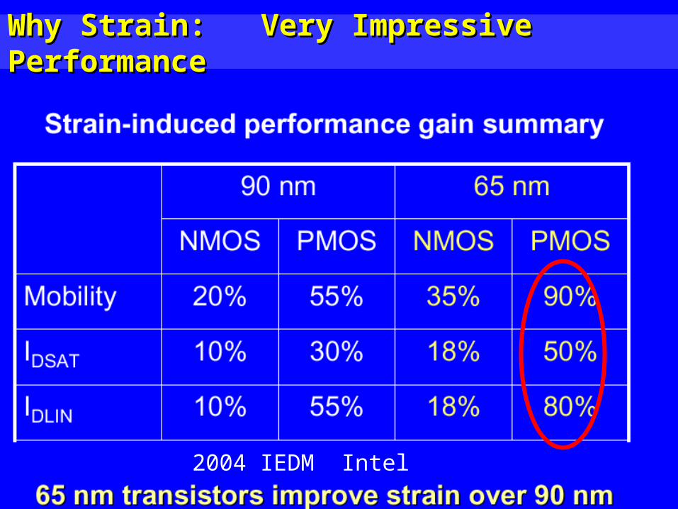
Why Strain: Very Impressive Performance Why Strain: Very Impressive Performance
2004 IEDM Intel
6
TI Fellows Forum
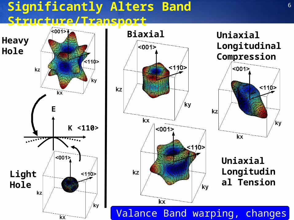
Significantly Alters Band Structure/Transport
E
K <110>
HeavyHole
Light Hole
UniaxialLongitudinal Compression
Biaxial Tension
Uniaxial Longitudinal Tension
Valance Band warping, changes m*,
7
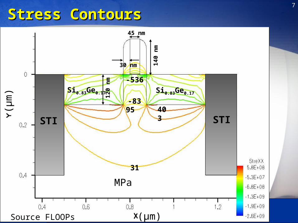
TI Fellows Forum (μm)
(μm
)
45 nm
140
nm
120
nm
30 nm
Si0.83Ge0.17Si0.83Ge0.17
STI STI
-536
-83403
95
31
Stress ContoursStress Contours
Source FLOOPs
MPa
8
TI Fellows Forum
Device Level Calibration: SRC/Intel FundedDevice Level Calibration: SRC/Intel Funded
• Industrial samples– 30 nm to 1um Si trasistors from 3 companies– Unstressed, uniaxial and biaxial stressed wafer– Bulk and SOI– Fully depleted SOI /Metal Gate– High k/metal gate and sub-micron Ge channel devices
9
TI Fellows Forum
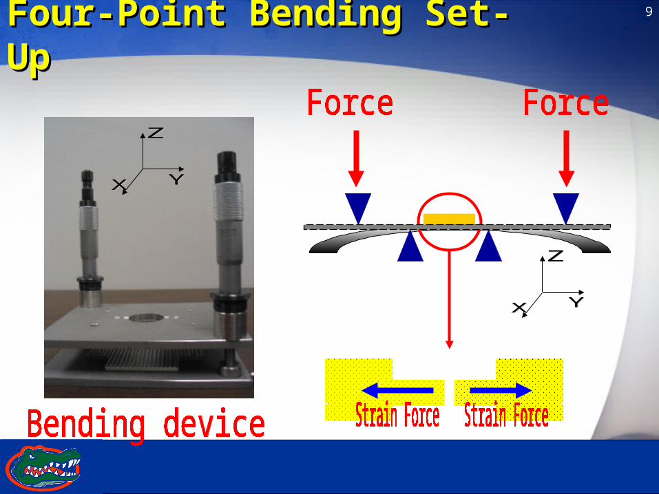
Four-Point Bending Set-UpFour-Point Bending Set-Up
10
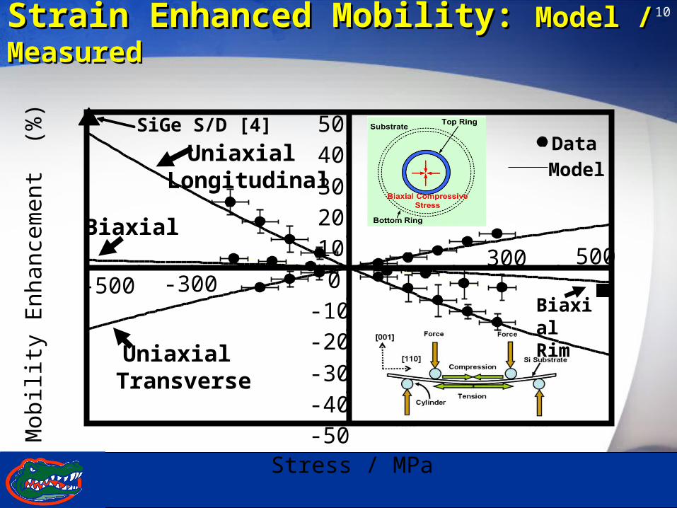
TI Fellows Forum
-50-40-30
-20-10
0
102030
4050
-500 -300300 500
Stress / MPa
Mob
ility
Enh
ance
men
t (
%)
Uniaxial Longitudinal
SiGe S/D [4]
Uniaxial Transverse
Biaxial
Biaxial Rim
DataModel
Strain Enhanced Mobility: Strain Enhanced Mobility: Model / MeasuredModel / Measured
11
TI Fellows Forum
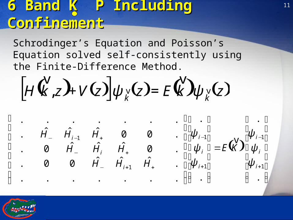
6 Band K P Including Confinement6 Band K P Including Confinement
( ) ( )[ ] ( ) ( ) ( )zkEzzVzkHkkvv
vvψψ =+,
( )
⎥⎥⎥⎥⎥⎥
⎦
⎤
⎢⎢⎢⎢⎢⎢
⎣
⎡
=
⎥⎥⎥⎥⎥⎥
⎦
⎤
⎢⎢⎢⎢⎢⎢
⎣
⎡
⎥⎥⎥⎥⎥⎥
⎦
⎤
⎢⎢⎢⎢⎢⎢
⎣
⎡
+
−
+
−
++−
+−
+−−
.
.
.
.
.......
.ˆˆˆ00.
.0ˆˆˆ0.
.00ˆˆˆ.
.......
1
1
1
1
1
1
i
i
i
i
i
i
i
i
i
KE
HHH
HHH
HHH
ψ
ψ
ψ
ψ
ψ
ψv
Schrodinger’s Equation and Poisson’s Equation solved self-consistently using the Finite-Difference Method.
12
TI Fellows Forum
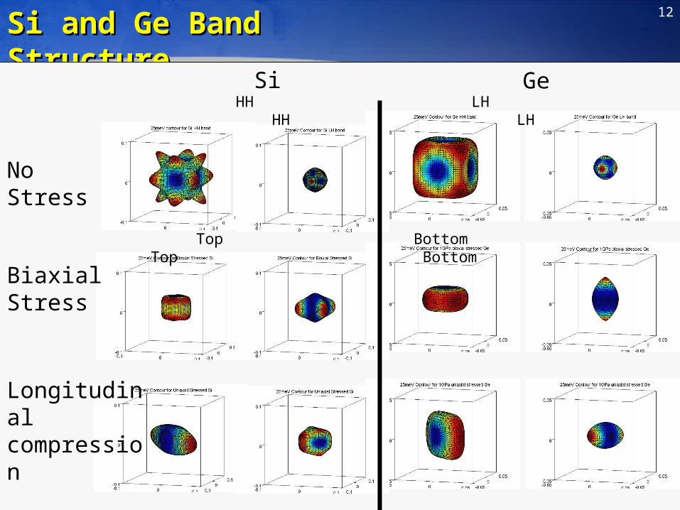
Si and Ge Band StructureSi and Ge Band Structure
GeSi
No Stress
Biaxial Stress
Longitudinal compression
HH LH HH LH
Top Bottom Top Bottom
13
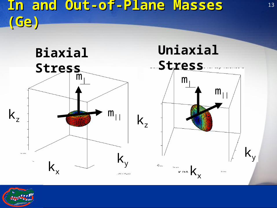
TI Fellows Forum
In and Out-of-Plane Masses (Ge)In and Out-of-Plane Masses (Ge)
m||
m|
m||
m|
kzkz
kyky
Uniaxial StressBiaxial Stress
kx kx
14
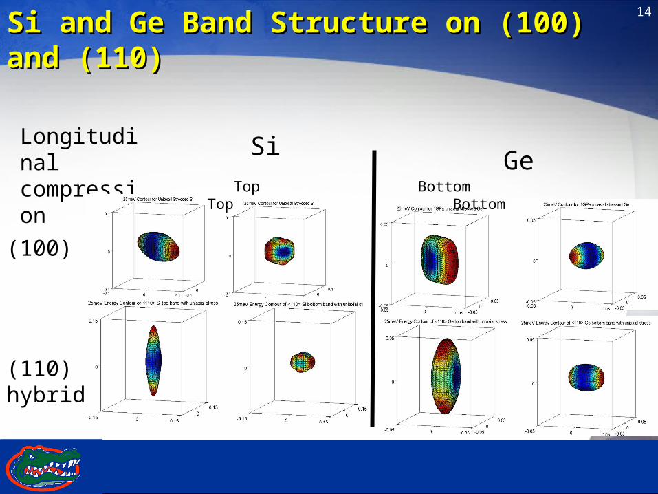
TI Fellows Forum
Si and Ge Band Structure on (100) and (110)Si and Ge Band Structure on (100) and (110)
SiGe
Longitudinal compression
Top Bottom Top Bottom
(100)
(110) hybrid
15
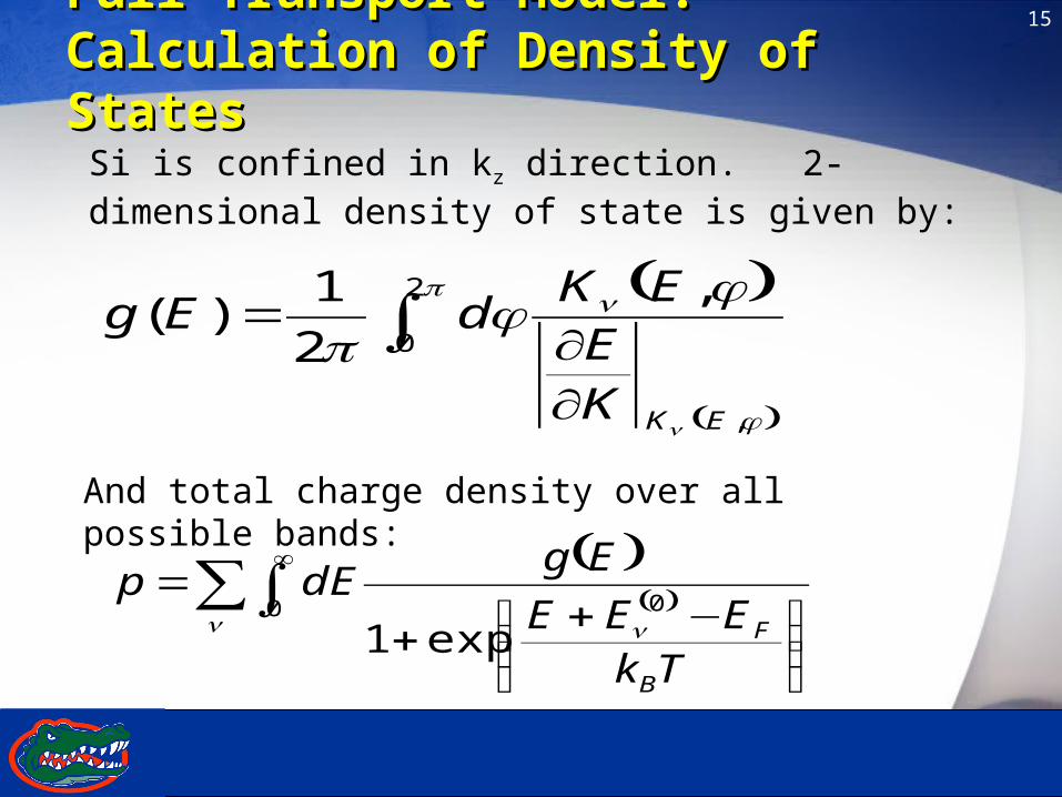
TI Fellows Forum
( )
( )
∫∂∂
=π
φ
ν
ν
φφπ
2
0
,
,
2
1)(
EKKE
EKdEg
Si is confined in kz direction. 2-dimensional density of state is given by:
And total charge density over all possible bands:
( )( )∑∫
∞
⎟⎟⎠
⎞⎜⎜⎝
⎛ −++=
ν ν0 0
exp1Tk
EEE
EgdEp
B
F
Full Transport Model: Calculation of Full Transport Model: Calculation of Density of StatesDensity of States
16
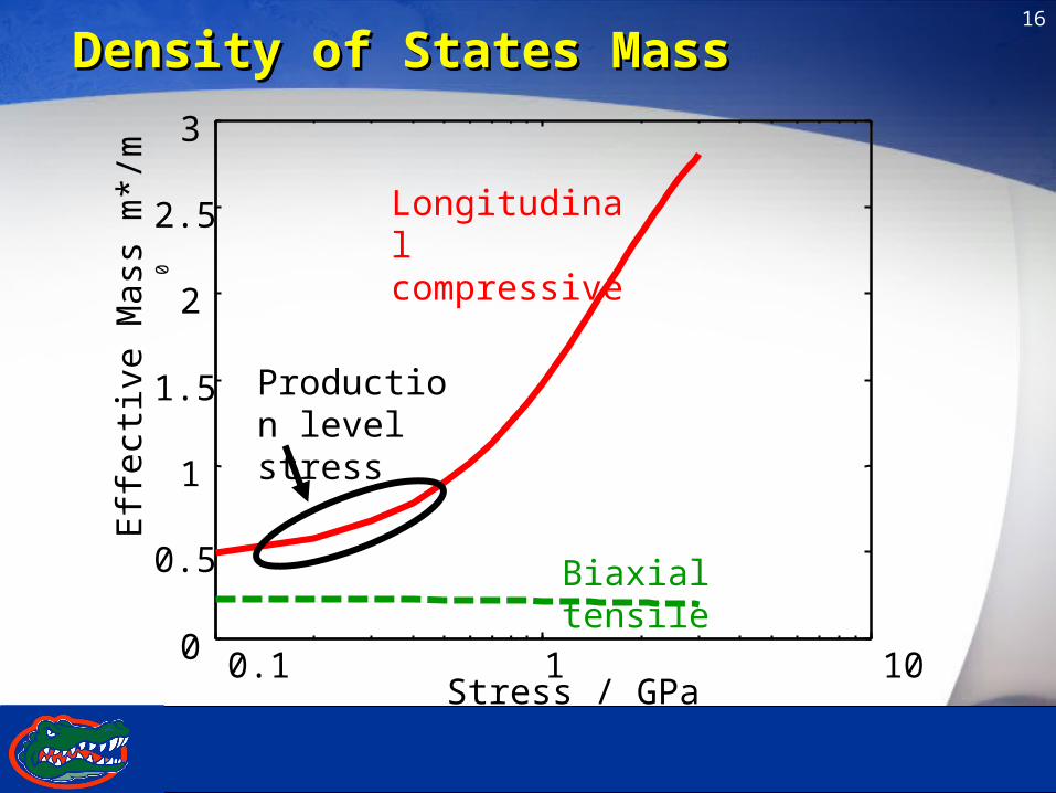
TI Fellows Forum
Density of States MassDensity of States Mass
0.1 1 10 0
0.5
1
1.5
2
2.5
3
Stress / GPa
Eff
ectiv
e M
ass
m*/
m0
Longitudinal compressive
Biaxial tensile
Production level stress
17
TI Fellows Forum
Summary / Next StepsSummary / Next Steps
• First-principles quantum mechanical methods for strained Si band structure
• Spatially dependent strain-induced band structure
• Model charge transport and collection due to single event in FLOOPS/FLOODS– Start with existing MURI developed models– Add strain for Si and Ge transistors


