Download - Nabih Edited Final Draft 1

7/27/2019 Nabih Edited Final Draft 1
http://slidepdf.com/reader/full/nabih-edited-final-draft-1 1/55
I. INTRODUCTION
A. BACKGROUND
In today’s military aviation, in the art of dogfighting, the primary objective is to
detect threats as early as possible in order to employ weapons effectively and to be
undetectable to increase survivability. The famous motto in the fighter pilot’s world is “to
stay alive, hide yourself and see your opponent before he sees you.” One side of the battle
is the high technology airborne radars; the other side is radar cross section reduction
techniques.
The two most often employed radar cross section reduction (RCSR) techniques
are shaping and use of radar absorbing materials for radar cross section reduction. Incurrent radar cross section (RCS) designs, shaping techniques are considered the first step
of RCS control. The objective of shaping is to design the platform’s surfaces and the
edges to reflect or diffract the incident wave in directions away form the radar, and is
primarily applied to establish a low RCS in the main threat sectors. However the
modification of an aircraft’s shape is limited to certain aerodynamic principles and within
last three decades, the shaping technique has been applied excessively in the design of
fighter aircraft such as the F-117. Recent design approaches generally opt for a balance
between shaping and other reduction techniques. Therefore, radar absorbing material
(RAM) engineering has become an important area of research.
Radar absorbing materials reduce the energy reflected back to the radar by means
of absorption. The technique is based on an arrangement of dielectric or magnetic
materials that present the appropriate impedance to the incident wave. The general idea is
to establish an impedance at the RAM surface that poses good matching and absorbing
qualities, so that it can attenuate the radar wave once it enters the material.
The use of radar absorbing material is one aspect of a comprehensive platform
design approach. It is a trade-off in which advantages are balanced against disadvantages,
and the systems engineering approach is applied. The use of radar absorbing materials
enables remarkable reduction in the platform’s radar cross section. On the other hand, it
has disadvantages like added weight, cost, and the requirement of high maintenance.
1

7/27/2019 Nabih Edited Final Draft 1
http://slidepdf.com/reader/full/nabih-edited-final-draft-1 2/55
In this study, the theory underlying radar absorbing material techniques is
summarized, with emphasis given to the matched surface impedance technique. This
technique employs combination of dielectric and magnetic materials to form an absorbing
layer that results in zero reflection over a specific range of wavelengths.
B. OBJECTIVES
The objective of this thesis is to summarize RCS, to analyze the theory related to
the matched surface RAM technique, and to generate universal design charts based on
matched surface RAM theory for specular absorbers. Numerical simulations of coated
plates are used to estimate the effectiveness of the layers in reducing RCS, and examine
the sensitivity of performance to small changes to the layer’s constituent parameters.
C. ORGANIZATION OF THESIS
In Chapter II, the methods of controlling radar cross section and penalties of
implementing these methods are discussed. The four basic techniques for reducing radar
cross section (target shaping, radar absorbing materials, passive cancellation, and active
cancellation) are summarized with their advantages and disadvantages. The two most
often employed methods, shaping and the use of radar absorbing materials, are examinedin detail.
In Chapter III, the basic theorems and theory underlying the use of radar
absorbing materials for RCS reduction are described, including the electronic loss
mechanisms. RAM design methods, the types of RAM structures, and various
implementations are discussed.
In Chapter IV, the analysis of matched surface RAM and zero specular reflection
absorbers are discussed. The equations related to specular absorbers are analyzed based
on the transmission line approach. Numerical methods for solving the transcendental
equations, and presentation of the results in the form of a universal design chart for zero
specular reflection are given.
2

7/27/2019 Nabih Edited Final Draft 1
http://slidepdf.com/reader/full/nabih-edited-final-draft-1 3/55
II. RADAR CROSS SECTION REDUCTION (RCSR)
TECHNIQUES
A. INTRODUCTION
This chapter evaluates methods of controlling RCS and the penalties in
implementing these methods. There are four basic techniques for reducing radar cross
section: (1) target shaping, (2) radar absorbing materials, (3) passive cancellation, and
(4) active cancellation.
Radar cross section reduction (RCSR) is a trade-off study in which the systems
engineering approach is applied, and advantages are balanced against disadvantages. For
example, the modification of an aircraft’s shape is limited to certain aerodynamic
principles. If radar absorbing materials (RAM) are used, monostatic radar cross section
reduction is obtained by the absorption of energy within the RAM, thus leaving the RCS
levels relatively unchanged in other directions. On the other hand, the use of RAM has
disadvantages like added weight, cost, and the requirement of high maintenance.
Reduction methods are generally limited to a small spatial region. The platform
design process must address how much RCS reduction is required based on the
platform’s mission, and the additional cost of manufacturing and maintenance.
B. THE FOUR BASIC TECHNIQUES OF RCSR
The following sections provide a summary of each RCSR technique. The two
most often applied ones, shaping and radar absorbing materials techniques, are examined
first. In current RCS designs, shaping techniques are primarily applied to establish a low
RCS in the main threat sections. Radar absorbing materials are then used to reduce the
effects of the creeping waves or traveling waves, or where shaping is not sufficient.
1. Shaping
5
Traditionally, shaping is considered the first step of RCS control. The objective of
shaping is to design the platform’s surfaces and edges to reflect or diffract the incident
RF wave in directions away form the radar. This cannot be accomplished for all aspect
angles, within the entire sphere of solid angles, because there will always be viewing
33

7/27/2019 Nabih Edited Final Draft 1
http://slidepdf.com/reader/full/nabih-edited-final-draft-1 4/55
angles at which surfaces are seen at normal incidence, and at these angles the echoes will
be high. The success of shaping depends on the existence of angular sectors over which
low radar cross section is less important than others. Shaping is a high-frequency
technique based on geometrical optics; it is implicit in this method that the target is very
large electrically [1].
It is usually best to keep large surfaces as flat and smooth as possible so that the
specular flash is confined to a very narrow angular region. The larger the area, the higher
the maximum RCS, and the faster it drops off [2]. For an aircraft the forward cone of
angles is the primary interest for RCSR. Hence, shifting the large cross sections out of the
forward sector toward broadside is desired. The forward section includes the elevation
plane as well as the azimuth plane. If a target is hardly ever seen from above, echo
sources, such as engine intakes, can be placed on the top side of the target where they
may be hidden by the forward portion of the body when viewed from below. Similarly,
for a low flyer such as a strike aircraft, whose major threats might be look-down radars,
engine inlets might instead be placed on the underside of the fuselage [1].
The Lockheed F-117A (Figure 1) is an example of heavily applied surface
faceting. Edges are parallel so that the majority of the edge effects are collectively
directed away from important viewing angles. The Northrop B-2 also uses some faceting,
especially on the trailing edges of the wing. In planform (Figure 2), the straight edges are
dominant [2].
For more “boxy” structures such as ships and ground vehicles, dihedral and
trihedral corners, and “top hats” (right circular cylinders with axes perpendicular to a flat
plane) are the major RCS contributors. They can be avoided by bringing intersecting
surfaces together at acute or obtuse angles. Because of the presence of the sea surface,
vertical bulkheads and masts on ships, in particular, form efficient corners, and the effect
can be reduced by tilting the bulkheads away from the vertical. However, this virtually
impossible to do with existing vessels and therefore is a real consideration only in new
designs. Even in the case of a new design, the amount of bulkhead tilt is a trade-off
between RCSR performance and cost [1].
64

7/27/2019 Nabih Edited Final Draft 1
http://slidepdf.com/reader/full/nabih-edited-final-draft-1 5/55
Figure 1. Planform of the Lockheed F-117 (After[3]).
Figure 2. Planform of the Northrop B-2 (After[3]).
75

7/27/2019 Nabih Edited Final Draft 1
http://slidepdf.com/reader/full/nabih-edited-final-draft-1 6/55
2. Radar Absorbing Materials
The radar absorbing materials reduce the energy reflected back to the radar by
means of absorption. Radar energy is absorbed through one or more of several
mechanisms, which may involve the dielectric or magnetic properties of the materials.
The loss is actually the conversion of radio frequency energy into heat, and although
most absorbers do not dissipate enough energy to become even detectably warm when
illuminated by a radar, this is nevertheless the mechanism by which they operate.
Underlying the operation of RAM is the fact that substances either exist or can be
fabricated whose indices of refraction are complex numbers. In the index of refraction,
which includes magnetic as well as electric effects, the imaginary part accounts for loss.
At microwave frequencies, the loss is due to the finite conductivity of the material, as
well as energy expended by molecules in attempting to follow the oscillating fields of an
impressed wave. It is customary to lump the effects of all loss mechanisms into the
permittivity and permeability of the material, both of which can be complex [1].
In summary, the requirements of a RAM for use in RCS reduction are: (1) the
absorbing material should have adequate frequency response, (2) it should work for two
orthogonal polarizations, and (3) it should work with the specified aspect angle
characteristics [4]. To choose a RAM that simultaneously satisfies all of these
requirements, and yet is physically realizable is difficult, if not impossible.
Considerations of weight and environment (e.g., temperature, rain, snow, etc.) play an
important role in deciding the thickness of any RAM coating.
The theory and analysis of RAM will be discussed further in Chapter III.
3. Passive Cancellation
Passive cancellation refers to RCS reduction by introducing a secondary scatterer
to cancel with the reflection of the primary target. This method is also known as
impedance loading.
The basic concept is to introduce an echo source whose amplitude and phase can
be adjusted to cancel another echo source. This can be accomplished for relatively simple
objects, provided that a loading point can be identified on the body. A port can be
8
6

7/27/2019 Nabih Edited Final Draft 1
http://slidepdf.com/reader/full/nabih-edited-final-draft-1 7/55
machined in that body, and the size and the shape of the interior cavity can be designed to
present optimum impedance at the aperture. Unfortunately, even for simple bodies, it is
extremely difficult to generate the required frequency dependence for this built-in
impedance, and the reduction obtained for one frequency rapidly disappears as the
frequency changes [1].
In addition to this, typical weapons platforms are hundreds of wavelengths in size
and have dozens, if not hundreds of echo sources. Clearly, it is not practical to devise a
passive cancellation treatment for each of these sources. Even when cancellation is
introduced at one frequency, the cancellation can revert to reinforcement with a small
change in frequency or viewing angle. It is evident that a fair amount of information
about the threat and the target itself is required: the threat radar frequency, direction, and
polarization, and the target RCS in the direction of the threat [1]. Note that there is a gray
area between the technologies of absorbing materials and passive cancellation. For
example, a layer of lossy dielectric coating applied to a target could fall into either
category.
4. Active Cancellation
Active cancellation involves the process of modifying and retransmitting the
received radar signal. The target must emit radiation in the same time with the received
pulse whose amplitude and phase cancel the reflected energy. The required data are the
angle of arrival, intensity, waveform and frequency of the received wave. An active
cancellation system should sense these data accurately and then reradiate the pulse with
proper amplitude and phase. Obviously, this requires a challenging task for the system, as
the frequency increases the work becomes much more difficult.
There are two levels of cancellation:
1. Fully active: The cancellation network receives, amplifies, and retransmits the
threat signal such that it is out of phase with the static RCS of the target. The transmitted
signal amplitude, phase, frequency and polarization can be adjusted to compensate for
changing threat parameters.
9
7

7/27/2019 Nabih Edited Final Draft 1
http://slidepdf.com/reader/full/nabih-edited-final-draft-1 8/55
2. Semiactive: No boost in threat signal energy is provided by the cancellation
network, but passive adjustable devices in the network allow the reradiated signal to
compensate for limited changes in the threat signal parameters [2].
The demands for a fully active system are almost always so severe as to make itimpractical. It requires a transmitter and antennas that cover the anticipated threat angles,
frequencies, incident power densities, and polarization. Knowledge of the threat direction
is required, as well as the target’s own RCS. A semiactive system is not as complicated
in terms of hardware, but the use of adjustable devices still requires bias lines, controller
units, and a computer with the appropriate data bases [2].
C. THE PENALTIES OF RCSR
Each of the described techniques of RCSR brings up its own disadvantages along
with its advantages and therefore requires trade-offs. The entire systems engineering
approach is required to evaluate the final system design.
The first and unavoidable penalty of RCSR is the additional cost. The others are:
reduced payload, added weight, required high maintenance, and reduced range or other
operational limitations. The mission of the platform and the severity of the threat
environment will determine the required RCSR and drive the trade-off study.
RCSR is just one aspect of the entire platform design which is affected by other
sensors and signatures (infrared, acoustic, visual, etc.). An optimum design must be
devised in order to maximize the objectives of the platform.
D. SUMMARY
In this chapter the four basic RCSR techniques were presented. Of the four, the
use of shaping and radar absorbing material design are the most used to date.
Shaping is considered the first step of RCS control, and it is broadband as long as
the wavelength is short compared to the platform dimensions (i.e., the “high frequency”
regime). The objective of shaping is to orient the target surfaces and the edges to deflect
the scattered energy in directions away form the radar.
108

7/27/2019 Nabih Edited Final Draft 1
http://slidepdf.com/reader/full/nabih-edited-final-draft-1 9/55
III. RADAR ABSORBING MATERIALS
A. INTRODUCTION
In addition to shaping an object to obtain a low radar cross section over a
specified range of aspect angles, the application of radar absorbing materials may further
reduce the radar cross section over a specified range of both frequencies and aspect
angles. Therefore the study of radar absorbing materials is crucial in order to minimize
the cross section of an object.
The technique is based on finding an arrangement of dielectric or magnetic
materials that can present the appropriate impedance to the incident wave. The general
idea is to establish a desirable impedance which poses good matching and absorbingqualities, so that the RAM can accept and then attenuate the incident wave.
In this chapter, the basic theory underlying absorbers is first illustrated, and then
the electronic loss mechanisms are presented. In the following parts, the design methods,
the types of current RAM structures, and various implementations are discussed.
B. ELECTROMAGNETIC LOSS MECHANISMS
At radar frequencies a reduction in reflection from an object can be achieved by
one of two mechanisms: (1) absorption, and (2) cancellation. Coatings, also referred as
resonant absorbers, reduce RCS by the cancellation of multiple reflections. Absorption is
transfer of incident wave’s energy to the material. The primary property of a radar
absorbing material is to dissipate the energy of the incident wave into heat. These
materials have constitutive parameters that are complex numbers.
The loss mechanisms are accounted for in the permittivity and permeability( )ε
( ) µ of the material. When expressing complex permittivity and permeability, the relative
permittivity and the relative permeability (( )r ε )r µ which are normalized by the free
space values ,0ε 0 µ are used.
The complex notation for andr ε r µ is normally given as
13
9

7/27/2019 Nabih Edited Final Draft 1
http://slidepdf.com/reader/full/nabih-edited-final-draft-1 10/55
0
0
( )
( )
r r
r r
j j
j j
ε ε ε ε ε ε
µ µ µ µ µ µ
′ ′′′ ′′= − = −
′ ′′′ ′′= − = −
,
, (3.3)
where the real part (energy storage part) is shown as a prime, and the imaginary part (loss
part) is shown as a double prime.
At microwave frequencies the absorbed energy can be transferred to the
molecules, similar to ohmic loss for conductors. As the wave energy is transferred to the
material the molecular dipoles oscillate. The loss amount is determined by the imaginary
parts of permeability and permittivity or, equivalently, the loss tangents,
,tan
tan .
ε
µ
ε δ ε
µ δ µ
′′=′
′′
= ′
(3.4)
They are called loss tangents because they are a measure of loss in the medium. The loss
tangents are typically in the range of 0.001-0.1 and therefore the attenuation of the wave
in decibels per meter is quite small. In the general case, the majority of loss for an electric
absorber is due to the finite conductivity of material. On the other hand, the loss for
magnetic absorbers is due to magnetization at microwave frequencies. Frequently it is
convenient to express the loss in terms of conductivity
0/r ε σ ωε ′′ = (3.5)
where is conductivity and is radian frequency. In polar notation, the relative values
are defined as
σ ω
r r
r r
j
j
e
e
ε
µ
δ
δ
ε ε
µ µ
=
=
(3.6)
The phase velocity in the medium is
. p
r r
cu
ω
β µ ε = =
′ ′
(3.7)
14
1 )
2 )
3 )
4 )
5 )
10
7/27/2019 Nabih Edited Final Draft 1
http://slidepdf.com/reader/full/nabih-edited-final-draft-1 11/55
Similarly, the intrinsic impedance is expressed in terms of r µ and as,r ε
0 r r η η µ ε = (3.8)
where 0η is the intrinsic impedance of free space, and equal to 120 or approximately
377 Ω .
π
In practical applications, a layer of dielectric will often be backed by a
conducting surface. In that case, a transmission line analysis can be performed to find the
effective input impedance at the front face of the layer [1]. For a flat metallic surface
coated with a thin layer of dielectric material (frequently called a Dallenbach layer), the
characteristic input impedance in Z is given by,
tanh( )r
o r r
r
in Z jk µ
t µ ε ε
= − (3.9)
where t is the thickness of the layer as shown in Figure 3. In the transmission line
equivalent, the reflection coefficient is defined as
0
0
,in
in
Z Z
Z Z
−Γ =
+ (3.10)
where it can be expressed as
0
0
1
1
in
in
Z Z
Z Z
−
Γ =
+
. (3.11)
It is clear from Equations (3.10) and (3.11) that if then0Γ =0in
Z Z = and the load is said
to be matched to the line. Thus, there will be no reflected wave at the outer face.
The objective of RAM design is to obtain a material for which the reflection
coefficient is as small as possible over as wide a frequency range as possible. It is clear
that unless the material has some loss, the amplitude of the reflection coefficient will be
controlled entirely by the phase and amplitude relationship between the portion of the
incident wave reflected at the front surface and the portion returning by reflections at the
backing surface [1].
15
6 )
7 )
8 )
9 )
8 ) 9 )
11

7/27/2019 Nabih Edited Final Draft 1
http://slidepdf.com/reader/full/nabih-edited-final-draft-1 12/55
Figure 3. Specular Reflection Schematic (After [2])
C. THEOREMS FOR ABSORBERS
Weston [5] developed two theorems for backscattering from absorber coated
conducting bodies that are illuminated by plane waves.
Theorem 1: If a target has equal values for relative permittivity and permeability,
that is,0
/ /ε ε 0
µ µ = at each point, then the backscattered field is zero, if the shape and
material of the body remain unchanged for a 90 degree rotation of the body around the
direction of incidence, which is also the direction of observation.
A wave incident along the axis of symmetry of a body of revolution satisfies the
geometric requirements of the theorem. If the body has constant permeability and
permittivity, they must be equal:r r
µ ε = [2].
16
Theorem 2: For a plane wave incident on a target, the backscattered fields will be
zero if the shape and constituent parameters of the target are invariant with respect to a 90
degree rotation around the direction of incidence (observation), and if the intrinsic
impedance of the material is equal to the impedance of free space, 0η η = , and the
following impedance boundary condition is satisfied on the surface of the body [4]:
12

7/27/2019 Nabih Edited Final Draft 1
http://slidepdf.com/reader/full/nabih-edited-final-draft-1 13/55
ˆ ˆ ˆ( ) ( E n E n n H η = = × )
i
(3.1)
where is the unit outward normal to the surface andn E
and H
are the electric and
magnetic fields of the incident plane wave,
0
0
0
0 ,
.
r
r
µ µ η η
ε ε
µ η
ε
= =
=
(3.2)
These theorems are derived directly from the Maxwell’s equations and the boundary
conditions which apply to any frequency and include all possible scattering and loss
mechanisms. Unfortunately, practical radar targets do not satisfy the geometry limitations
imposed by the theorems. However, the condition thatr r
µ ε = does shed some insight
into the reduction problem. Because the impedance of a medium relative free space is
essentially determined by /r r µ ε
0
, equal permeability and permittivity yield an
impedance in the medium Z . Consequently, the reflection coefficient between the free
space and the medium is zero. Note that this applies only to the specular field.
Diffractions from the edges and surface waves could still yield a nonzero scattered field
for a finite interface. The nonspecular contributions to scattering will be zero only if the
above- mentioned geometrical conditions are satisfied [2].
D. DIELECTRIC MULTILAYER ABSORBER DESIGN AND
PERFORMANCE
The objective in the design of radar absorbing material is to obtain a layer (or
layers) of the least thickness, having the lowest reflection coefficient, operating within a
wide frequency range, easily applied, low-cost, light weight and long-lasting.
In the following sections the RAM types that are commonly used are depicted
based on their design characteristics and performance. The descriptions start with
17
1 )
2 )
13

7/27/2019 Nabih Edited Final Draft 1
http://slidepdf.com/reader/full/nabih-edited-final-draft-1 14/55
Salisbury screens and Dallenbach layers which are the two oldest and most basic types of
absorbers. Then the discussion is extended to broadband absorbers.
1. Salisbury Screens and Dallenbach Layers
The Salisbury screen (Figure 4) is formed by placing a resistive sheet above the
object’s surface in order to create a resonant absorber. If the resistive film is from
the conductor, then a quarter-wavelength transmission line section transforms the short
circuit at the conductor plate into an open circuit (conductance, G=0 ). Thus,
/ 4λ
1 1 1 1
in s s
. Z R R
= + =∞
(3.12)
The reflection coefficient will be zero when . Recall that, when the line is
quarter-wave length or , where n=0 or a positive integer, a matched load is
provided and no reflection occurs. Therefore, the Salisbury screen is most effective at
normal incidence.
377 s R = Ω
/ 4 / 2nλ λ +
For oblique incidence of a plane wave onto the absorber, the magnitude of the
reflection coefficients for parallel and perpendicular polarizations are expressed in terms
of θ
1 cos.
1 cos
θ
θ ⊥
−Γ = Γ −
+ (3.13)
In Figure 5, Equation (3.13) is plotted or angles up to 35o, where is the angle off-
normal. Where the reflection coefficient is smaller than 0.1, the performance is better
than 20 dB.
θ
For other values of resistivity or spacing, the cancellation is not complete. Neither
is it complete for a finite screen size, even for ideal materials, because of edge
diffractions from the screen and ground plane [2]. Rapid oscillations for large spacings
render the absorber ineffective over a wide frequency range [1].
18
10 )
11 )
14

7/27/2019 Nabih Edited Final Draft 1
http://slidepdf.com/reader/full/nabih-edited-final-draft-1 15/55
Figure 4. Salisbury Screen (After [2])
The Dallenbach layer (Figure 6) consists of a homogeneous lossy layer backed by
a metal plate. Similar to the Salisbury screen, the reflection from the outer surface cancels
the reflection from the back surface. From Equation (3.10), the reflection coefficient at
the outer surface is
in o
in o
Z Z
Z Z
−Γ =
+
where
11
1
tanh( )tanh( )
load
in
load
Z jZ t Z Z Z jZ t
γ γ
+=+
(3.14)
19
12 )
15

7/27/2019 Nabih Edited Final Draft 1
http://slidepdf.com/reader/full/nabih-edited-final-draft-1 16/55
Figure 5. Reflection coefficient as a function of angle of incidence
Z 1 is the impedance of the layer material, Z load is the impedance of the back material and
t is thickness of the outer surface. The impedance Z 1 can be written as
1 . j
Z j
µ µ µ ε ε ε
′ −= =
′ ′−
′′
′ (3.15)
The complex propagation constant is
. jγ ω µε = (3.16)
As it is clearly seen, the reflection at the surface of a material is due to the
impedance change seen by the wave at the interface between the two media. Therefore, if
a material can be found whose impedance relative to the free space equals 1 (i.e.,
r r µ ε = ), there will be no reflection at the surface. In this case the attenuation will depend
on the loss properties of the material ( , )r r
ε µ ′′ ′′ and electrical thickness. Unfortunately,
materials with the appropriate dielectric and magnetic properties to act as a matched
RAM over any frequency bandwidth are difficult to find. So the objective is to optimize
the loss at the given frequency with available material.
20
13 )
14 )
16

7/27/2019 Nabih Edited Final Draft 1
http://slidepdf.com/reader/full/nabih-edited-final-draft-1 17/55
Figure 6. Dallenbach Layer (After [2])
Figure 7. Performance of Dallenbach Layers (From [2]).
Figure 7 shows the reflection coefficient of Dallenbach layers as a function of
thickness for various values of permeability and permittivity. The best RCSR
performance for nonmagnetic materials occurs at quarterwave length (0.25 , is the0λ 0λ
21
17

7/27/2019 Nabih Edited Final Draft 1
http://slidepdf.com/reader/full/nabih-edited-final-draft-1 18/55
free space wavelength) where 1, 1r r µ ε = > and second resonance occurs at 0.50λ o where
1, 1r r ε µ = > for magnetic materials.
2. Multilayer Dielectric Absorbers
One objective of RAM design is to have the radar absorbing material efficient
over a wide range of frequencies. However, by using a single-layer absorber the
bandwidth obtained is generally insufficient. The multilayer dielectric absorber concept
benefits from the change of effective impedance with the distance into the material, so
that the reflections are minimized. Two important multilayer dielectric absorbers will be
discussed in this section: (1) Jaumann absorbers, and (2) graded dielectric absorbers.
Jaumann absorbers are formed by positioning the multilayer resistive sheets from
the sheet with the highest resistivity in the front and the lowest one at the back, so that the
bandwidth of a Salisbury screen can be improved. Theoretically the bandwidth of
Jaumann absorber may be three times that of a single Salisbury screen [4]. Figure 8
shows the reflected power versus frequency for absorbers with numerous resistive sheets.
It is evident that theoretically the frequency bandwidth is increased with the increase in
the number of layers. For this illustration, the spacing between sheets is at 7.5 mm (a
quarter wavelength at 10 GHz) and a quadratic resistance taper is used. Note that the
four-sheet structure has about four times the fractional bandwidth of a single layer [1]. In
Table 1 the relationship between the number of sheets, fractional bandwidth and total
thickness is listed.
Table 1. The number of sheets versus fractional bandwidth (From [1]).
22
18

7/27/2019 Nabih Edited Final Draft 1
http://slidepdf.com/reader/full/nabih-edited-final-draft-1 19/55
Figure 8. The predicted performance of Jaumann multilayer absorbers (From [1]).
The graded dielectric absorbers are constructed of discrete layers with properties
changing from layer to layer. A technique for reducing the reflection from the front face
of a flat absorber is to produce a material whose intrinsic impedance is very close to unity
by employing conductivity gradient up to certain degree. Two common examples are thehair-type and the carbon-loaded low density foam absorbers [1].
Since the structural property and RCSR performance of the hair-type absorbers
are poor compared to pyramidal absorbers and graded dielectrics, hair-type absorbers are
not widely used.
Carbon-loaded foam using geometric transition from a free space into a lossy
media is another type of graded absorber. The transition to the lossy medium establishes
a dielectric gradient and the reflections are reduced. This type of absorber is usually in
the form of pyramids or wedges of rubber or plastic foam which is loaded with an
electrically lossy materials such as carbon. In Figure 8 a sketch of such absorber is
shown. Geometric absorbers are generally not used in target RCSR applications because
of the large volume they occupy.
23
19

7/27/2019 Nabih Edited Final Draft 1
http://slidepdf.com/reader/full/nabih-edited-final-draft-1 20/55
Figure 9. Geometric transition absorber (From [1]).
E. MAGNETIC RAM
Magnetic RAM, such as ferrite slabs, have distinct advantages over dielectric
absorbers, since magnetic RAM only requires one-tenth of the thickness of the dielectric
absorber to achieve the same RCS reduction. Magnetic materials have relative
permeabilites different than that of free space. To this point, the RCSR approaches have
employed a complex relative permittivity with a non-magnetic material ( 1 0r j µ = + ).
Clearly the intrinsic impedance of such a material is and the index of refraction
is
377/r
ε
r ε . Having the relative permeability other than one, enables further modification of
intrinsic impedance and index of refraction, and consequently the resulting absorption
performance gets better.
24
The magnetic materials that are available for use in RAM generally have relative
permittivities higher than their relative permeabilities. Therefore, practically speaking,
20

7/27/2019 Nabih Edited Final Draft 1
http://slidepdf.com/reader/full/nabih-edited-final-draft-1 21/55
pure magnetic (non dielectric) materials with , do not exist [1]. Research in
materials science has lead to artificial materials constructed of dielectric and magnetic
components that have a wide range of and
1r
jε = +
r
0
r ε µ . In most applications, iron and
components of iron are most preferred. The two most common materials employed inRAM are carbonyl iron and ferrites suspended in a dielectric.
The main difference between magnetic and electric material is the thickness
required for the first resonance. Magnetic RAM, despite of the fact that it is heavy, can
operate at low frequencies with reasonable thickness. The thickness required for a
magnetic RAM to obtain low-frequency coverage down to 100 MHz, is much less than
one tenth that of a dielectric absorber.
In reference [6] it is shown that for a Dallenbach layer, the lowest possible
reflection ( Γ ) is related to the widest operating band ( ∆ ) by0 λ
0
0
0
2
r r d
λ
λ π ε µ λ
Γ ∆=
−
(3.17)
where is the center frequency. The bandwidth for a thin layer becomes0λ 0(t λ )
0
32Re .r t λ µ
π ∆ ≈ Γ (3.18)
This illustrates the necessity for a high permeability layer if it is to be thin and large.λ ∆
The loss increases at low frequencies with the increasing r µ . On the other hand,
the relative dielectric constant changes linearly with the frequency increase (Figure 10).
As the frequency increases the magnetic properties do not affect the loss, however the
electric properties start to contribute to loss.
25
15 )
16 )
21

7/27/2019 Nabih Edited Final Draft 1
http://slidepdf.com/reader/full/nabih-edited-final-draft-1 22/55
Figure 10. Schematic illustration of the frequency behavior of ferrites. (From [1])
Figure 11. Thin-film magnetodielectric as used in circuit applications (From [1])
The suspended particle approach to constructing magnetic material can be applied
on a macroscopic scale. The magnetic losses can be manipulated by arranging layers of
thin magnetic films in dielectric, as shown in Figure 11. These are referred to as thin-film
26
22
7/27/2019 Nabih Edited Final Draft 1
http://slidepdf.com/reader/full/nabih-edited-final-draft-1 23/55
magnetodielectrics (TFM). The thin films increase the surface area exposed to the wave
and circumvent the skin depth limitations encountered with a conducting magnetic
material [2].
F. MATCHED SURFACE RAM
The discussions in Section D show that choosing the appropriate dielectric and
magnetic properties of a material will produce zero specular reflection. Two different
concepts have been introduced in specular reflection reduction applications: (1) matched
characteristic impedance, and (2) matched wave impedance.
The goal is to find a material whose impedance in combination with backing
material is equal to the intrinsic impedance of the free space. In other words, the relative
dielectric constant of the material and the relative magnetic permeability of the material
is equal to each other at every point. Musal and Smith [7] refer to concept as the
“matched-characteristic impedance” approach in which there is no front-surface
reflection for normal incidence from the material layer. Making the layer thick enough so
that internal attenuation along the round-trip path through the material reduces the
emerging wave to an acceptably low amplitude eliminates any reflection from the
backing material.
The second approach in specular reflection reduction is the “matched wave
impedance” approach [7]. The idea is that the wave impedance at the front surface of the
reflector-backed material layer is made equal to the intrinsic impedance of the free space,
thus producing no reflection at all. In this study, following chapters are dedicated to the
concept of matched wave impedance approach for theoretical analysis and applications in
various materials.
G. OTHER RADAR ABSORBING STRUCTURES
Traditional studies of RAM have always considered absorber as an “add on”
material with its own specifications and properties, which cause additional weight and
extra design considerations. However, communities like aviation persistently aim to cut
27
23

7/27/2019 Nabih Edited Final Draft 1
http://slidepdf.com/reader/full/nabih-edited-final-draft-1 24/55
down on weight, and have started designing RAM as an integral composite part of the
object. This approach may involve combining several absorber designs, and therefore are
called hybrid RAMs.
An example of a hybrid RAM for broadband operations that includes low-frequency applications, which has a front layer of Jaumann absorbers or graded dielectric
and back layer material of magnetic material. At low frequencies the magnetic material
is clearly superior (Figure 10) and at microwave frequencies the front layers of dielectric
RAM would provide the attenuation. Figure 12 provides predicted data for a three-layer
Jaumann absorber, a four-layer graded dielectric absorber (dipped core honeycomb, for
example), and a hybrid formed by combining a Jaumann with a graded dielectric. Each
layer is 7.55mm. thick, so the total RAM thickness is 3 cm. Note that the use of the
combined techniques provides both improved low-frequency performance and good
performance through K u band [1].
Figure 12. Reflection coefficient as a function of frequency (From[1])
The circuit analog technique introduces the idea of representing the geometrical
patterns in terms of effective resistance, capacitance, and inductance, and then equivalent
circuit techniques are used in the design of the resulting absorber.
28
24

7/27/2019 Nabih Edited Final Draft 1
http://slidepdf.com/reader/full/nabih-edited-final-draft-1 25/55
Salisbury screens and Jaumann absorbers employ resistive sheets that only have
real part of the admittance. Clearly, flexibility can be obtained if the sheets have
susceptance as well as conductance. Figure 13 shows circuit analog geometries like
dipoles, crosses or triangles. In any event, the reason for employing circuit analog sheets
rather than simple resistive sheets in an absorber is to provide increased bandwidth
through increased control of the impedance properties of the lossy material.
Figure 13. Typical circuit analog element geometries (From [1])
H. NONSPECULAR RAM
The nonspecular returns are from surface traveling waves, edge waves, creeping
waves, the gaps, cracks and edge diffractions. In order to deal with the surface wave and
traveling waves returns two different approaches have been employed: (1) magnetic and
dielectric surface coatings and (2) tapered resistive sheets.
Magnetic RAM is employed most effectively in close contact with a perfectly
conducting surface where the magnetic field has its highest value. It has been known that
29
25

7/27/2019 Nabih Edited Final Draft 1
http://slidepdf.com/reader/full/nabih-edited-final-draft-1 26/55
a thin coating of magnetic RAM could effectively reduce traveling and creeping wave
returns [1]. The approach to the calculating of the effects of a surface coating on traveling
wave amplitude follows the analysis of lossy surface wave transmission line.
The incident wave has an electric field in the z −
plane, and the associatedmagnetic field in free space is given by
exp[ ( )] yo o o H H j z h x β = − (3.18)
with the propagation constants 0 β and such thatoh
2 22 (2 / )o o o oh k 2 β π λ + = = (3.19)
where is the free space wavelength. A similar set of equations holds for the magnetic
field inside the layer, with the values of
0λ
,h β and λ depending on the thickness of the
layer and the properties of the coating (i.e., 1 0 1 1k k µ ε = ). For the guided wave case, the
impedance at the boundary must match for the two waves (the free-space wave and the
one in the coating layer) [1]. A matched condition occurs with 0 1 x x s Z Z Z = = , where
ox Z is , and377Ω s Z is the surface (or input) impedance of the coating. Matching
impedances and solving for the equivalent of Equation (3.18) in the material gives
0 /377. sh k Z = (3.20)
The value of h can then be substituted into Equation (3.19) to find . β
The parameter of interest is the attenuation of the -traveling wave provided by
the coating, and that is given by the imaginary part of the
z
, β where
22
0(2 / )(1 / 377 ) . s Z β π λ = −1/ 2 (3.21)
The surface impedance of the layer will depend on the angle of the incidence of theincoming wave. However, for large andε µ values, the direction of the refracted ray in
the material layer will be very close to the normal, regardless of the incidence angle. The
attenuation per wavelength of travel in the -direction in the layer is then given by z
08.69Im dB/ L β λ = (3.22)
30
17 )
18 )
19 )
20 )
21 )
26

7/27/2019 Nabih Edited Final Draft 1
http://slidepdf.com/reader/full/nabih-edited-final-draft-1 27/55
In Figure 14, the surface wave attenuation per wavelength of propagation as a
function of layer thickness for a thin magnetic RAM coating is shown. The attenuation
rises rapidly with increasing thickness, but peaks and then begins rapidly decreasing. The
decrease occurs as the surface impedance begins to go from inductive to capacitive, and
layer begins to shed, rather than trap, a surface wave. The peak loss for the material
shown is about 28 and occurs for a layer thickness of about 0.037 , or 1 cm
at 1 GHz [1].
0dB/λ 0dB/λ
Scattering also arises from the impedance discontinuities on a body. Those
discontinuities can be due to changes in materials (e.g., transition from a metal fuselage
to a nonconducting canopy), or they can be geometric (a discontinuity in any derivative
of the surface contour provides a theoretical opportunity for backscatter, although
discontinuities with radii of curvature greater than a wavelength can generally be
ignored). Clearly, two of the most severe discontinuities possible are sharp edges and
corners, but they are also structures that often appear on vehicles designed for low RCS
because of their natural occurrence in application of the shaping rules [1].
Edges and corners are important constituents in three different types of scattering.
First, perpendicular to a leading edge for parallel polarization or a trailing edge for
perpendicular polarization, there is an edge diffraction return given as .
Corners provide a lower level, but relatively isotropic, diffraction return. Also, edges and
corners provide the area from which physical optics end-region returns rise. Finally,
edges and corners provide discontinuities that reflect surface traveling waves and edge
waves, giving the opportunity for return in the backscatter direction [1].
2 2/ m Lσ π ≈
Therefore, the treatment of edges can potentially reduce threat sector RCS levels
for all three of the major scattering mechanisms expected in a vehicle shaped for low
RCS. As in the design of specular RAM, wideband edge treatments must provide slowly
varying impedance to taper the transition between free space and the body being treated.
31
27

7/27/2019 Nabih Edited Final Draft 1
http://slidepdf.com/reader/full/nabih-edited-final-draft-1 28/55
Figure 14. Surface wave attenuation as a function of layer thickness (From [1])
I. SUMMARY
The main objective in radar absorbing material design is to set the RAM
parameters in order to allow the wave to enter the layer and then provide sufficient loss to
absorb the energy within RAM thickness. The two requirements generally conflict, since
high-loss materials often have intrinsic impedances different that of free-space and thus
suffer high front-face reflections.
Two basic solutions are applied to address the problem. Tapering the loss from
the front to the back of the absorber with Jaumann, graded electric and geometric
transition absorbers is one of the solutions. The major disadvantage of these methods is
the increased thickness for low frequencies. The other solution is the employment of
tuned but high loss materials. The purpose is to establish a matched transmission line
32
28

7/27/2019 Nabih Edited Final Draft 1
http://slidepdf.com/reader/full/nabih-edited-final-draft-1 29/55
between free space and the material in order to cancel out the reflections. Magnetic
materials are best for this condition but in practice the frequency bandwidth is quite
limited. In order to increase the bandwidth, the hybrid materials can be used. In spite of
the fact that the hybrid materials can provide significant performance in a reasonable
thickness, problems in production and maintenance and high cost are the disadvantages.
This chapter is dedicated to describing various types of RAM and discussions of
their performance characteristics. The crucial issue in RAM employment is the trade-off
study between cost, maintenance, performance, and ease of manufacturing. A systems
engineering study will dictate the most reasonable solution for a particular target and its
intended mission.
33
29

7/27/2019 Nabih Edited Final Draft 1
http://slidepdf.com/reader/full/nabih-edited-final-draft-1 30/55
LIST OF REFERENCES
1. Eugene F. Knott, John F. Schaeffer, Michael T. Tuley, Radar Cross Section, 2nd
edition, Artech House, 1993.
2. David C. Jenn, Radar and Laser Cross Section Engineering , AIAA, 1995.
3. Federation of American Scientist Official Website (www.fas.org), 22 June 2003.
4. Asoke Bhattacharyya, D.L. Sengupta, Radar Cross Section Analysis & Control ,
Artech House, 1991.
5. V. H. Weston, “Theory of Absorbers in Scattering,” IEEE Transactions on
Antennas and Propagation, Vol. AP, No. 4, September 1963.
6. Geoge T. Ruck, Donald E. Barrick, William D. Stuart, Calerence K. Krichbaum,
Radar Cross Section Handbook , 2nd
edition, 1970.
7. H. M. Musal, Jr., D. C. Smith, “Universal Design Chart for Specular Absorbers,”
IEEE Transactions on Magnetics, Vol. 26, No. 5, September 1990.
8. B. C. Hoskin, A. A. Baker, Composite Materials for Aircraft Structures, AIAA,
1986.
9. M. Dresselhaus, G. Dresselhaus, K. Sugihara, I. Spain, H. A. Goldberg Graphite
Fibers and Filaments, Springer-Verlag Berlin Heidelberg, 1988.
10. Fawwaz T. Ulaby, Fundamentals of Applied Electromagnetics, Media Edition,
Prentice Hall, 2001.
65

7/27/2019 Nabih Edited Final Draft 1
http://slidepdf.com/reader/full/nabih-edited-final-draft-1 31/55
Measurement of Radar Cross Section
Introduction
To establish the stealthiness of a platform, it could simply be built and then tested againstthe threat radar. The obvious danger in this approach is that deficiencies occurring in the
early stages of the design would not be uncovered until completion and, thus, could not be corrected. Another complication is that the effective measured RCS will depend on the
radar parameters and test environment. For these reasons, the precise quantity of RCS as
defined is measured in a controlled environment. In general, measured RCS data can
serve three purposes:
1) To establish a target's RCS for design verification.
2) For comparison with calculated RCS, to evaluate numerical methods, approximations,
and so forth.
3) As a diagnostic or troubleshooting tool.
Measurements play an important part in the design of a stealthy platform. During theconceptual stage, scale models of candidate designs might be built and tested to verify
that the RCS levels are in the ballpark and that no unexpected scattering arises. At
various stages in the development of the full-scale components (such as wings and
antennas), measurements can be used to verify assembly tolerances, RCS treatments, andother manufacturing processes. Problem areas can be reworked and then remeasured.
Finally, if the target is not too large, a measurement can be made on the completed
product. This step may serve as the official fulfillment of a contract.
Measurement facilities can be categorized by a wide variety of attributes, which include physical characteristics, instrumentation capabilities, and data analysis and presentation.
Table 8.1 summarizes some commonly used descriptors. Most systems measure
monostatic RCS by using a fixed transmit/receive antenna and rotating the target. 1 First,
a known calibration target like a sphere is measured, and its received power is recordedas a reference. Next, the sphere is replaced by the object with unknown RCS, and the
process is repeated as the target is rotated. By comparing the received power to the
reference power, the RCS of the unknown target is obtained. In older systems the scaled
power difference is sent to a plotter that is slewed to the target mount. The final result is a
plot of RCS vs aspect angle.
The classical far-field continuous wave (CW) RCS measurement is illustrated in Fig. 8.1.
For a true far-field measurement, the target must be illuminated by a plane wave. This
condition is never rigorously satisfied in practice because the need for a directive transmit
antenna usually results in a nonuniform amplitude illumination of the target.

7/27/2019 Nabih Edited Final Draft 1
http://slidepdf.com/reader/full/nabih-edited-final-draft-1 32/55
Furthermore, the wave incident on the target is always spherical, not planar. Finally,
because the system components are near the surface, reflections from the ground and
other obstacles will affect the measurement.Several measures of chamber performanceare 1) pattern symmetry, 2) noise floor (noise level), 3) quiet zone, 4) repeatability, 5)
allowable target size and weight, 6) allowable range of target motion, 7) instrumentation
capabilities, 8) data processing capabilities, and 9) data presentation capabilities. Asample plot from a CW measurement is shown in Fig. 8.2. It illustrates the types ofinaccuracies that occur, such as sidelobe asymmetry and the existence of a noise floor.
The noise floor sets a lower limit on the RCS than can be reliably measured.These will be
discussed in some detail in the following sections.
Chamber Configurations
The majority of all RCS measurement facilities are completely enclosed (indoor ranges),
providing isolation from the external environment, which is desirable for both security
and technical reasons. An indoor chamber has reduced or eliminated interference fromother radio frequency (rf) sources and a controlled temperature for increased
instrumentation stability. The end result is more accurate and repeatable measurements
7/27/2019 Nabih Edited Final Draft 1
http://slidepdf.com/reader/full/nabih-edited-final-draft-1 33/55
than are possible in an outdoor facility. The obvious limitation to an indoor chamber is
the size of the building required for large targets.
7/27/2019 Nabih Edited Final Draft 1
http://slidepdf.com/reader/full/nabih-edited-final-draft-1 34/55
Conditions for Plane Wave Incidence
Figure 8.3 shows three types of indoor chambers. The first is the standard farfield
configuration. The separation of the antenna and target must be large enough so that the
difference between an ideal plane wave and the actual spherical wave is negligible. The
required distance is a function of target size and the frequency. If the distance is R andthe target length L, as indicated in Fig. 8.4, the phase error at the edge of the target
relative to the center is
The right-hand side of Eq. (8.1) holds for R >> L. Based on the convention used for the
definition of the far field of a radiating antenna, we might limit the round-trip phase error
to , so that Eq. becomes
Solving for R, the minimum distance is

7/27/2019 Nabih Edited Final Draft 1
http://slidepdf.com/reader/full/nabih-edited-final-draft-1 35/55
For example, at 6 GHz, a target with length L = 1 m should be at least 320 m from thesource. This distance turns out to be overly restrictive and is usually not adhered to in
practice. Equation (8.1) assumes that all the target surface contributes coherently to the
total RCS, for example, a smooth plate. On the other hand, if the target is composed ofmany independent scatterers, the far-field distance is determined primarily by the
dominant scatterers and their distribution in space. Thus, when the dominant scatterers
are "clustered," a much smaller range will suffice. 2 In addition to a plane phase front at
the target, the amplitude of the incident wave across the target must be constant. Theamplitude distribution is controlled by the antenna beamwidth and the ratio L/R. An
isotropic antenna provides the most uniform wave front but also results in strongerillumination of the chamber walls and other obstacles. The transmitted power level mustalso be higher if the antenna gain is low. Thus, there is a tradeoff necessary to determine
the optimum antenna beamwidth.
Compact Ranges
The demands on chamber size required for accurate low-RCS measurementshave resulted
in the development of compact ranges. The layout of a typical compact range is shown in
Fig. 8.5. The parent reflector configuration is a Cassegrain, and the reflector surfaceshave been arranged so that no blockage occurs. The transmit/receive antenna is located at
the focus, and a plane wave field is formed a short distance in front of the paraboloid.The total volume of a compact range is much less than that of an equivalent far-field
configuration. Figure 8.6 shows a compact range at the U.S. Navy's facility in PointMugu, California. The compact range is not without its own problems. To obtain uniform
amplitude over the target requires a shaped feed pattern or some subreflector shaping.
Cross polarization and edge diffraction can be significant. Because the target is close tothe reflector edges, the effects of edge scattering are especially important at low RCS
levels. Much effort has gone into the design of rolled or serrated edges that control the

7/27/2019 Nabih Edited Final Draft 1
http://slidepdf.com/reader/full/nabih-edited-final-draft-1 36/55
level and direction of edge diffraction. The state-of-the-art instrumentation used in RCS
measurement is essentially a programmable multimode radar. 3'4 Data can be collected in
either the time or frequency domain and transformed back and forth between the two. Inthe time domain, gating or windowing can be employed to discard signals that do not
correspond to the time delay of a scattered signal from the target's location.

7/27/2019 Nabih Edited Final Draft 1
http://slidepdf.com/reader/full/nabih-edited-final-draft-1 37/55
Sources of Measurement Error
The received signal in a measurement is not due entirely to scattering from the target. It
also includes noise introduced by the receiving system and extraneous scattered signals
originating from the chamber walls and other obstacles, as illustrated in Fig. 8.7. Some of
the transmit signal couples directly to the receive antenna. This leakage is strongest when
a common antenna is used for both transmit and receive.
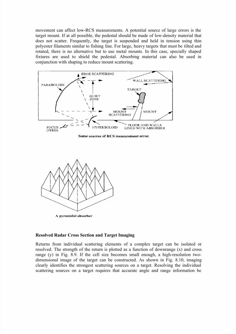
Chambers that are used to measure low or very low RCS must be carefully designed,
maintained, and calibrated. Great care is taken to reduce the error signals in the vicinity
of the target. The volume of the chamber that is essentially free of extraneous signals isreferred to as the quiet zone. It is usually specified in feet or meters and is perhaps the
most important figure of merit of an RCS facility. It represents the largest diameter of a
sphere in which a centered target can be rotated while maintaining the phase and
amplitude error specifications of the chamber. The quiet zone and the operating
frequency range effectively define the chamber performance.
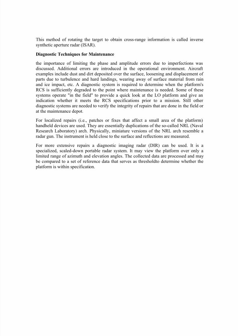
If the test range is indoors, then ideally the walls should be perfect absorbers it is clearthat the walls cannot be made perfect absorbers and, therefore, error signals corrupt the
RCS pattern measurements. A technique for reducing the reflection from the front face of
a flat absorber is to produce a material whose intrinsic impedance is very close to unity.Achieving the impedance gradient by geometrical shaping of a medium of constant
impedance provides a more complete transition from free space to the loading medium.
Geometrical shaping means replacing the front face of the surface with shaped pointedelements such as cones or pyramids, where the axis of individual elements is oriented
transverse to the plane of the absorber. A wave entering such a medium encounters a
smoothly changing ratio of medium to the adjacent free space. This is similar to the case
where the actual properties are changing gradually. Two examples are the "horse-hair"
type and the carbon-loaded low-density foam absorbers. The most common one is the pyramidal absorber, illustrated in Fig. 8.8. The faceted faces of the pyramidal absorber
cause dispersion of the incident plane wave by causing reflections and diffractions in alldirections, thereby reducing the RCS in the transverse plane. This type of absorber can
provide reflectivity reductions in excess of 50 dB but may require a thickness in excess of
10)~ to achieve such a level.
Measurement errors are mitigated using background subtraction. First, a measurement is
taken with the target absent. Ideally, the received signal should be zero if the chamberwalls are perfect absorbers and there is no leakage. In practice, a nonzero signal is
present, stemming from the sources indicated in Fig. 8.7, and this value is stored as a
reference. Next, the measurement is repeated with the target present. The measured value
will include the target's RCS as well as the error signals. If the interaction between thetarget and chamber is negligible, vector subtraction of the background signal should yield
a close approximation to the isolated target's RCS.
The subtraction method requires that the characteristics of the measurement equipment
remain stable during the calibration and measurement runs. If the power level orfrequency drifts, the background reference is no longer valid, and the difference is
erroneously attributed to the target. Even small changes in phase caused by cable
7/27/2019 Nabih Edited Final Draft 1
http://slidepdf.com/reader/full/nabih-edited-final-draft-1 38/55
movement can affect low-RCS measurements. A potential source of large errors is the
target mount. If at all possible, the pedestal should be made of low-density material that
does not scatter. Frequently, the target is suspended and held in tension using thin polyester filaments similar to fishing line. For large, heavy targets that must be tilted and
rotated, there is no alternative but to use metal mounts. In this case, specially shaped
fixtures are used to shield the pedestal. Absorbing material can also be used inconjunction with shaping to reduce mount scattering.
Resolved Radar Cross Section and Target Imaging
Returns from individual scattering elements of a complex target can be isolated or
resolved. The strength of the return is plotted as a function of downrange (x) and crossrange (y) in Fig. 8.9. If the cell size becomes small enough, a high-resolution two-
dimensional image of the target can be constructed. As shown in Fig. 8.10, imaging
clearly identifies the strongest scattering sources on a target. Resolving the individualscattering sources on a target requires that accurate angle and range information be

7/27/2019 Nabih Edited Final Draft 1
http://slidepdf.com/reader/full/nabih-edited-final-draft-1 39/55
available as the returns are received. Range resolution is achieved by using a short pulse
of duration r that illuminates only a small slice of the target, as shown in Fig. 8.11.
Knowledge of the time elapsedafter the leading edge of the pulse hits the target is
equivalent to knowledge of thedownrange coordinate y.
One method of obtaining the cross-range value x is by accurately pointing a narrowantenna beam as shown in Fig. 8.11. The beam is scanned over the entire solid angle of
the target, thereby providing angle data that can be processed along with the range data to
construct an image. This approach is not efficient at microwave frequencies, however, because of the large antenna size needed for fine angle resolution. It is more practical at
millimeter wavelengths and smaller and is highly successful at laser wavelengths.
A more practical method for obtaining cross-range takes advantage of the Doppler shift.The target is rotated at an angular frequency cor, as shown in Fig. 8.12. Target surface

7/27/2019 Nabih Edited Final Draft 1
http://slidepdf.com/reader/full/nabih-edited-final-draft-1 40/55
points rotate with a linear velocity that depends on their distance from the center of
rotation. The component of velocity parallel to R gives rise to a Doppler shift.
Referring to the coordinate system shown in Fig. 8.13, let R0 be the range to the target
center of rotation along the y coordinate and r the distance to a scattering point at a
distance d from the center. When the law of cosines is used,
which simplifies to
when R0 >> d. The instantaneous value of the monostatic scattered electric field varies as
The term (wt) in the argument is associated with the carrier and -2kRo with the round-trip
time delay to and from the target center; 2kd sin 4~ is the Doppler shift
due to rotation. Since , the Doppler frequency in hertz is
7/27/2019 Nabih Edited Final Draft 1
http://slidepdf.com/reader/full/nabih-edited-final-draft-1 41/55
This method of rotating the target to obtain cross-range information is called inverse
synthetic aperture radar (ISAR).
Diagnostic Techniques for Maintenance
the importance of limiting the phase and amplitude errors due to imperfections was
discussed. Additional errors are introduced in the operational environment. Aircraft
examples include dust and dirt deposited over the surface, loosening and displacement of parts due to turbulence and hard landings, wearing away of surface material from rain
and ice impact, etc. A diagnostic system is required to determine when the platform's
RCS is sufficiently degraded to the point where maintenance is needed. Some of these
systems operate "in the field" to provide a quick look at the LO platform and give anindication whether it meets the RCS specifications prior to a mission. Still other
diagnostic systems are needed to verify the integrity of repairs that are done in the field or
at the maintenance depot.
For localized repairs (i.e., patches or fixes that affect a small area of the platform)
handheld devices are used. They are essentially duplications of the so-called NRL (NavalResearch Laboratory) arch. Physically, miniature versions of the NRL arch resemble a
radar gun. The instrument is held close to the surface and reflections are measured.
For more extensive repairs a diagnostic imaging radar (DIR) can be used. It is a
specialized, scaled-down portable radar system. It may view the platform over only a
limited range of azimuth and elevation angles. The collected data are processed and may be compared to a set of reference data that serves as thresholdto determine whether the
platform is within specification.

7/27/2019 Nabih Edited Final Draft 1
http://slidepdf.com/reader/full/nabih-edited-final-draft-1 42/55
Understanding the Fundamental Principles of Vector NetworkAnalysis
Introduction
Network analysis is the process by which designers and manufacturers measure the
electrical performance of the components and circuits used in more complex systems.
When these systems are conveying signals with information content, we are mostconcerned with getting the signal from one point to another with maximum efficiencyand minimum distortion. Vector network analysis is a method of accurately
characterizing such components by measuring their effect on the amplitude and phase of
swept-frequency and swept-power test signals.In this application note, the fundamental principles of vector network analysis will be
reviewed. The discussion includes the common parameters that can be measured,
including the concept of scattering parameters (S-parameters). RF fundamentals such as
transmission lines and the Smith chart will also be reviewed.Agilent Technologies offers a wide range of portable and benchtop vector network
analyzers for characterizing components from DC to 110 GHz. These instruments are
available with a wide range of options to simplify testing in the field, laboratory, and production environments.
Measurements in Communications Systems
In any communications system, the effect of signal distortion must be considered. While
we generally think of the distortion caused by nonlinear effects (for example, when
intermodulation products are produced from desired carrier signals), purely linearsystems can also introduce signal distortion. Linear systems can change the time
waveform of signals passing through them by altering the amplitude or phase
relationships of the spectral components that make up the signal.
Let’s examine the difference between linear and nonlinear behavior more closely.
Linear devices impose magnitude and phase changes on input signals (Figure 1).
Any sinusoid appearing at the input will also appear at the output, and at the same
frequency. No new signals are created. Both active and passive nonlinear devices canshift an input signal in frequency or add other frequency components, such as harmonic
and spurious signals. Large input signals can drive normally linear devices into
compression or saturation, causing nonlinear operation.
For linear distortion-free transmission, the amplitude response of the device under test(DUT) must be flat and the phase response must be linear over the desired bandwidth. As
an example, consider a square-wave signal rich in high-frequency components passing
through a bandpass filter that passes selected frequencies with little attenuation whileattenuating frequencies outside of the passband by varying amounts.

7/27/2019 Nabih Edited Final Draft 1
http://slidepdf.com/reader/full/nabih-edited-final-draft-1 43/55
Even if the filter has linear phase performance, the out-of-band components of the square
wave will be attenuated, leaving an output signal that, in this example, is more sinusoidal
in nature (Figure 2).If the same square-wave input signal is passed through a filter that only inverts the phase
of the third harmonic, but leaves the harmonic amplitudes the same, the output will be
more impulse-like in nature (Figure 3). While this is true for the example filter, ingeneral, the output waveform will appear with arbitrary distortion, depending on theamplitude and phase nonlinearities.

7/27/2019 Nabih Edited Final Draft 1
http://slidepdf.com/reader/full/nabih-edited-final-draft-1 44/55
Nonlinear devices also introduce distortion (Figure 4). For example, if an amplifier isoverdriven, the output signal clips because the amplifier is saturated. The output signal is
no longer a pure sinusoid, and harmonics are present at multiples of the input frequency.
Passive devices may also exhibit nonlinear behavior at high power levels, a good

7/27/2019 Nabih Edited Final Draft 1
http://slidepdf.com/reader/full/nabih-edited-final-draft-1 45/55
example of which is an L-C filter that uses inductors with magnetic cores. Magnetic
materials often exhibit hysteresis effects that are highly nonlinear.
Efficient transfer of power is another fundamental concern in communications systems.In order to efficiently convey, transmit or receive RF power, devices such as
transmissions lines, antennas and amplifiers must present the proper impedance match to
the signal source. Impedance mismatches occur when the real and imaginary parts ofinput and output impedances are not ideal between two connecting devices.
Importance of Vector Measurements
Measuring both magnitude and phase of components is important for several reasons.
First, both measurements are required to fully characterize a linear network and ensure
distortion-free transmission. To design efficient matching networks, complex impedance
must be measured. Engineers developing models for computer-aided-engineering (CAE)circuit simulation programs require magnitude and phase data for accurate models.
In addition, time-domain characterization requires magnitude and phase information in
order to perform an inverse-fourier transform. Vector error correction, which improvesmeasurement accuracy by removing the effects of inherent measurement-system errors,
requires both magnitude and phase data to build an effective error model. Phase-
measurement capability is very important even for scalar measurements such as return
loss, in order to achieve a high level of accuracy.
The Basis of Incident and Reflected Power
In its fundamental form, network analysis involves the measurement of incident,
reflected, and transmitted waves that travel along transmission lines. Using opticalwavelengths as an analogy, when light strikes a clear lens (the incident energy), some of
the light is reflected from the lens surface, but most of it continues through the lens (the
transmitted energy) (Figure 5). If the lens has mirrored surfaces, most of the light will bereflected and little or none will pass through it.
While the wavelengths are different for RF and microwave signals, the principle is the
same. Network analyzers accurately measure the incident, reflected, and transmittedenergy, e.g., the energy that is launched onto a transmission line, reflected back down the
transmission line toward the source (due to impedence mismatch), and successfully
transmitted to the terminating device (such as an antenna).
7/27/2019 Nabih Edited Final Draft 1
http://slidepdf.com/reader/full/nabih-edited-final-draft-1 46/55
The Smith Chart
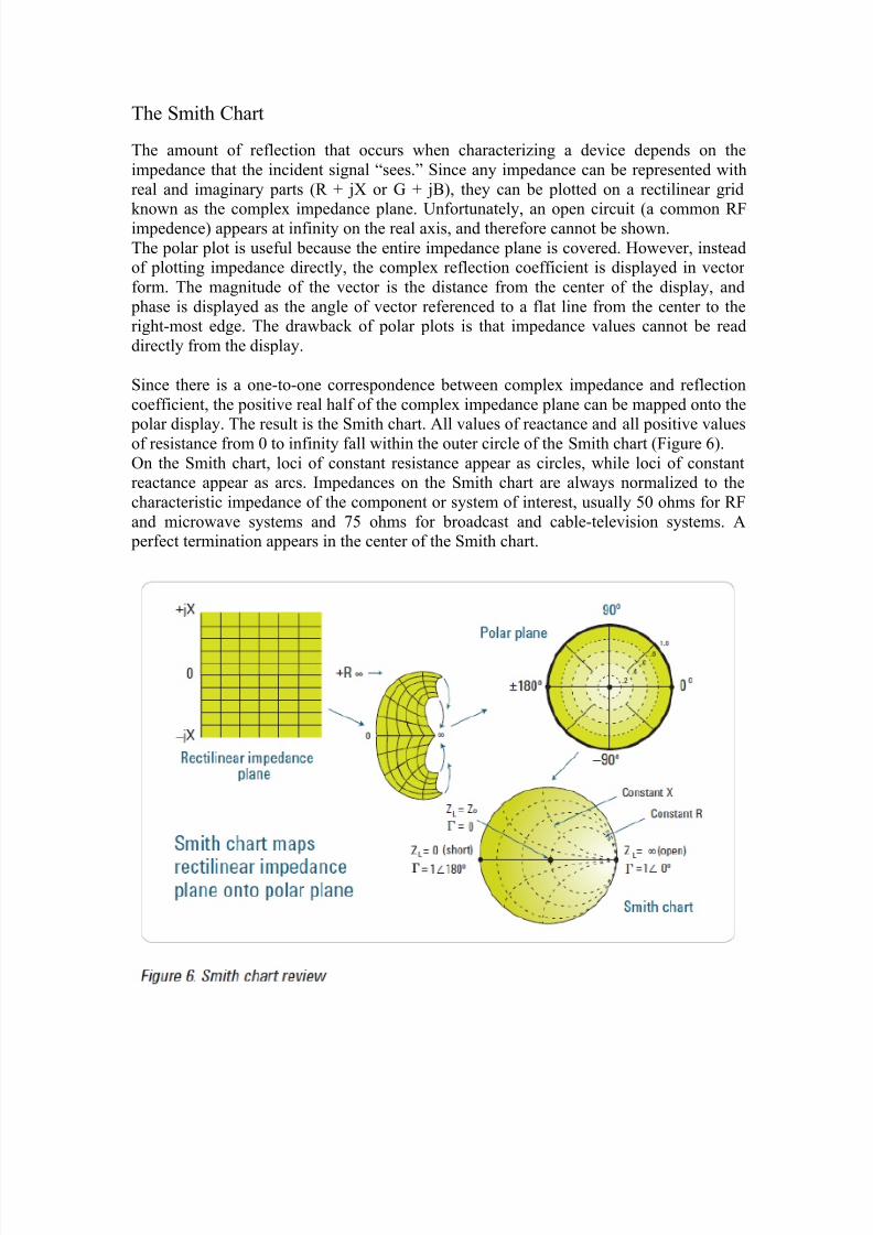
The amount of reflection that occurs when characterizing a device depends on the
impedance that the incident signal “sees.” Since any impedance can be represented with
real and imaginary parts (R + jX or G + jB), they can be plotted on a rectilinear grid
known as the complex impedance plane. Unfortunately, an open circuit (a common RFimpedence) appears at infinity on the real axis, and therefore cannot be shown.
The polar plot is useful because the entire impedance plane is covered. However, insteadof plotting impedance directly, the complex reflection coefficient is displayed in vector
form. The magnitude of the vector is the distance from the center of the display, and
phase is displayed as the angle of vector referenced to a flat line from the center to theright-most edge. The drawback of polar plots is that impedance values cannot be read
directly from the display.
Since there is a one-to-one correspondence between complex impedance and reflection
coefficient, the positive real half of the complex impedance plane can be mapped onto the
polar display. The result is the Smith chart. All values of reactance and all positive valuesof resistance from 0 to infinity fall within the outer circle of the Smith chart (Figure 6).
On the Smith chart, loci of constant resistance appear as circles, while loci of constantreactance appear as arcs. Impedances on the Smith chart are always normalized to the
characteristic impedance of the component or system of interest, usually 50 ohms for RF
and microwave systems and 75 ohms for broadcast and cable-television systems. A perfect termination appears in the center of the Smith chart.

7/27/2019 Nabih Edited Final Draft 1
http://slidepdf.com/reader/full/nabih-edited-final-draft-1 47/55
Power Transfer Conditions
A perfectly matched condition must exist at a connection between two devices for
maximum power transfer into a load, given a source resistance of RS and a loadresistance of RL. This condition occurs when RL = RS, and is true whether the stimulus
is a DC voltage source or a source of RF sine waves (Figure 7).When the source impedance is not purely resistive, maximum power transfer occurs
when the load impedance is equal to the complex conjugate of the source impedance.This condition is met by reversing the sign of the imaginary part of the impedance. For
example, if RS = 0.6 + j 0.3, then the complex conjugate is RS* = 0.6 – j 0.3.
The need for efficient power transfer is one of the main reasons for the use oftransmission lines at higher frequencies. At very low frequencies (with much larger
wavelengths), a simple wire is adequate for conducting power. The resistance of the wire
is relatively low and has little effect on low-frequency signals. The voltage and current
are the same no matter where a measurement is made on the wire.
At higher frequencies, wavelengths are comparable to or smaller than the length of theconductors in a high-frequency circuit, and power transmission can be thought of in termsof traveling waves. When the transmission line is terminated in its characteristic
impedance, maximum power is transferred to the load. When the termination is not equal
to the characteristic impedance, that part of the signal that is not absorbed by the load isreflected back to the source.
If a transmission line is terminated in its characteristic impedance, no reflected signal
occurs since all of the transmitted power is absorbed by the load (Figure 8). Looking at
the envelope of the RF signal versus distance along the transmission line shows nostanding waves because without reflections, energy flows in only one direction.

7/27/2019 Nabih Edited Final Draft 1
http://slidepdf.com/reader/full/nabih-edited-final-draft-1 48/55
When the transmission line is terminated in a short circuit (which can sustain no voltageand therefore dissipates zero power), a reflected wave is launched back along the line
toward the source (Figure 9). The reflected voltage wave must be equal in magnitude to
the incident voltage wave and be 180 degrees out of phase with it at the plane of the load.
The reflected and incident waves are equal in magnitude but traveling in the oppositedirections.
If the transmission line is terminated in an open-circuit condition (which can sustain nocurrent), the reflected current wave will be 180 degrees out of phase with the incident
current wave, while the reflected voltage wave will be in phase with the incident voltage
wave at the plane of the load. This guarantees that the current at the open will be zero.The reflected and incident current waves are equal in magnitude, but traveling in the
opposite directions. For both the short and open cases, a standing wave pattern is set up
on the transmission line. The voltage valleys will be zero and the voltage peaks will be
twice the incident voltage level.
If the transmission line is terminated with say a 25-ohm resistor, resulting in a condition between full absorption and full reflection, part of the incident power is absorbed and partis reflected. The amplitude of the reflected voltage wave will be one-third that of the
incident wave, and the two waves will be 180 degrees out of phase at the plane of the
load. The valleys of the standing-wave pattern will no longer be zero, and the peaks will
be less than those of the short and open cases. The ratio of the peaks to valleys will be2:1.

7/27/2019 Nabih Edited Final Draft 1
http://slidepdf.com/reader/full/nabih-edited-final-draft-1 49/55
The traditional way of determining RF impedance was to measure VSWR using an RF
probe/detector, a length of slotted transmission line, and a VSWR meter. As the probe
was moved along the transmission line, the relative position and values of the peaks andvalleys were noted on the meter. From these measurements, impedance could be derived.
The procedure was repeated at different frequencies. Modern network analyzers measure
the incident and reflected waves directly during a frequency sweep, and impedanceresults can be displayed in any number of formats (including VSWR).
Network Analysis Terminology
Now that we understand the fundamentals of electromagnetic waves, we must learn the commonterms used for measuring them. Network analyzer terminology generally denotes measurementsof the incident wave with the R or reference channel. The reflected wave is measured with the Achannel, and the transmitted wave is measured with the B channel (Figure 10). With theamplitude and phase information in these waves, it is possible to quantify the reflection andtransmission characteristics of a DUT. The reflection and transmission characteristics can beexpressed as vector (magnitude and phase), scalar (magnitude only), or phase-only quantities.For example, return loss is a scalar measurement of reflection, while impedance is a vector
reflection measurement. Ratioed measurements allow us to make reflection and transmissionmeasurements that are independent of both absolute power and variations in source powerversus frequency. Ratioed reflection is often shown as A/R and ratioed transmission as B/R,relating to the measurement channels in the instrument.
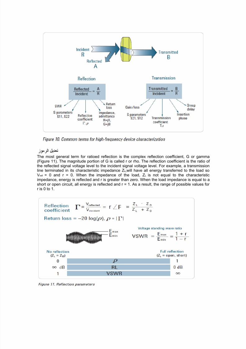
7/27/2019 Nabih Edited Final Draft 1
http://slidepdf.com/reader/full/nabih-edited-final-draft-1 50/55
عديل رموزThe most general term for ratioed reflection is the complex reflection coefficient, G or gamma(Figure 11). The magnitude portion of G is called r or rho. The reflection coefficient is the ratio ofthe reflected signal voltage level to the incident signal voltage level. For example, a transmissionline terminated in its characteristic impedance Zo,will have all energy transferred to the load soVrefl = 0 and r = 0. When the impedance of the load, ZL is not equal to the characteristicimpedance, energy is reflected and r is greater than zero. When the load impedance is equal to a
short or open circuit, all energy is reflected and r = 1. As a result, the range of possible values forr is 0 to 1.

7/27/2019 Nabih Edited Final Draft 1
http://slidepdf.com/reader/full/nabih-edited-final-draft-1 51/55
Return loss is a way to express the reflection coefficient in logarithmic terms (decibels).
Return loss is the number of decibels that the reflected signal is below the incident signal.
Return loss is always expressed as a positive number and varies between infinity for aload at the characteristic impedance and 0 dB for an open or short circuit. Another
common term used to express reflection is voltage standing wave ratio (VSWR), which is
defined as the maximum value of the RF envelope over the minimum value of the RFenvelope. It is related to r as (1 + r)/(1 – r). VSWR ranges from 1 (no reflection) toinfinity (full reflection).
The transmission coefficient is defined as the transmitted voltage divided by the incident
voltage (Figure 12). If the absolute value of the transmitted voltage is greater than theabsolute value of the incident voltage, a DUT or system is said to have gain. If the
absolute value of the transmitted voltage is less than the absolute value of the incident
voltage, the DUT or system is said to have attenuation or insertion loss. The phase
portion of the transmission coefficient is called insertion phase.
Direct examination of insertion phase usually does not provide useful information. This is becausethe insertion phase has a large (negative) slope with respect to frequency due to the electricallength of the DUT. The slope is proportional to the length of the DUT. Since it is only deviationfrom linear phase that causes distortion in communications systems, it is desirable to remove the
linear portion of the phase response to analyze the remaining nonlinear portion. This can be doneby using the electrical delay feature of a network analyzer to mathematically cancel the averageelectrical length of the DUT. The result is a high-resolution display of phase distortion or deviationfrom linear phase (Figure 13).

7/27/2019 Nabih Edited Final Draft 1
http://slidepdf.com/reader/full/nabih-edited-final-draft-1 52/55
Measuring Group Delay
Another useful measure of phase distortion is group delay (Figure 14). This parameter is
a measure of the transit time of a signal through a DUT versus frequency. Group delaycan be calculated by differentiating the DUT’s phase response versus frequency. It
reduces the linear portion of the phase response to a constant value, and transforms the
deviations from linear phase into deviations from constant group delay, (which causes phase distortion in communications systems). The average delay represents the average
signal transit time through a DUT.
Depending on the device, both deviation from linear phase and group delay may be measured,since both can be important. Specifying a maximum peak-to-peak phase ripple in a device maynot be sufficient to completely characterize it, since the slope of the phase ripple depends on the

7/27/2019 Nabih Edited Final Draft 1
http://slidepdf.com/reader/full/nabih-edited-final-draft-1 53/55
number of ripples that occur per unit of frequency. Group delay takes this into account because itis the differentiated phase response. Group delay is often a more easily interpreted indication ofphase distortion (Figure 15).
Network Characterization
In order to completely characterize an unknown linear two-port device, we must makemeasurements under various conditions and compute a set of parameters. These
parameters can be used to completely describe the electrical behavior of our device (or
network), even under source and load conditions other than when we made our
measurements. Low-frequency device or network characterization is usually based onmeasurement of H, Y, and Z parameters. To do this, the total voltage and current at the
input or output ports of a device or nodes of a network must be measured. Furthermore,measurements must be made with open-circuit and short-circuit conditions. Since it is difficult to measure total current or voltage at higher frequencies, S-parameters
are generally measured instead (Figure 16). These parameters relate to familiar
measurements such as gain, loss, and reflection coefficient. They are relatively simple tomeasure, and do not require connection of undesirable loads to the DUT. The measured
S-parameters of multiple devices can be cascaded to predict overall system performance.
S-parameters are readily used in both linear and nonlinear CAE circuit simulation tools,
and H, Y, and Z parameters can be derived from S-parameters when necessary.The number of S-parameters for a given device is equal to the square of the number of
ports. For example, a two-port device has four S-parameters. The numbering conventionfor S-parameters is that the first number following the S is the port at which energyemerges, and the second number is the port at which energy enters. So S21 is a measure
of power emerging from Port 2 as a result of applying an RF stimulus to Port 1. When the
numbers are the same (e.g. S11), a reflection measurement is indicated.
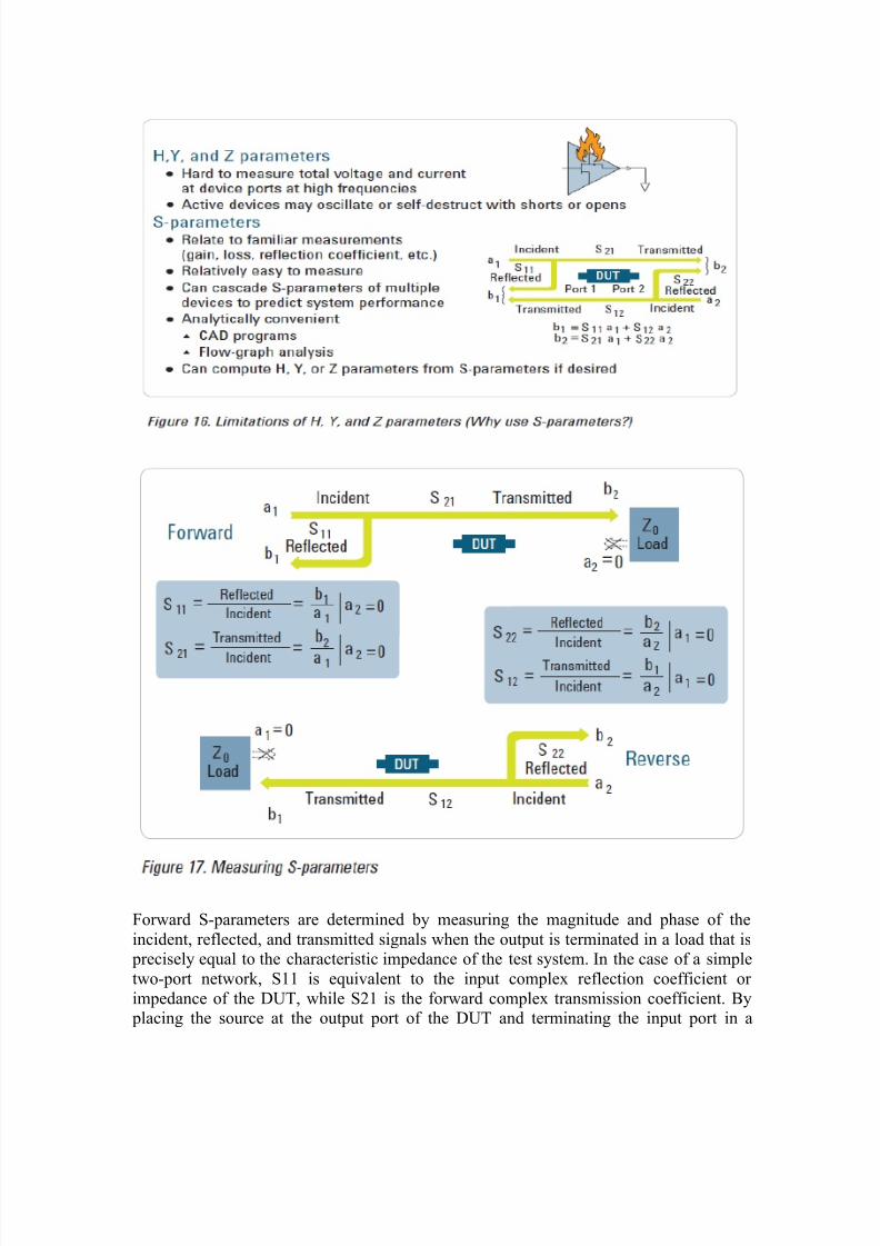
7/27/2019 Nabih Edited Final Draft 1
http://slidepdf.com/reader/full/nabih-edited-final-draft-1 54/55
Forward S-parameters are determined by measuring the magnitude and phase of the
incident, reflected, and transmitted signals when the output is terminated in a load that is precisely equal to the characteristic impedance of the test system. In the case of a simple
two-port network, S11 is equivalent to the input complex reflection coefficient or
impedance of the DUT, while S21 is the forward complex transmission coefficient. By placing the source at the output port of the DUT and terminating the input port in a

7/27/2019 Nabih Edited Final Draft 1
http://slidepdf.com/reader/full/nabih-edited-final-draft-1 55/55
perfect load, it is possible to measure the other two (reverse) S-parameters. Parameter
S22 is equivalent to the output complex reflection coefficient or output impedance of the
DUT while S12 is the reverse complex transmission coefficient (Figure 17).


