Download - Nanotech Insights

Graphene Derived Porous Carbon for CO2 Capture
Mass Production of High-Quality Graphene: Global Patent Analysis
ALD Coatings for Multifunctional Applications
Fighting Diabetes with Nanotechnology
Nano S&T: Indian Scenario
A quarterly newsletter dedicated to nanoscience and nanotechnologyA quarterly newsletter dedicated to nanoscience and nanotechnology
Insights
April 2012 Volume 3 Issue 2 RNI No. APENG/2010/34023ISSN 2229-5992
NanotechNanotech
Conductive Inks & Paints
Polymer Fillers Battery Electrodes Supercapacitors
Sensors
Touch Screens Smart Windows
Flexible LCDs & OLEDs Solar Cells
Research Purpose
FETs Interconnects
NEMs Composites
Polymer Fillers Transparant Electrodes
Sensors
Transistors Circuits
Interconnects Memory
Semiconductors
Small Scale Production
High Cost
High Quality
Uneven Films
Epitaxial Growth on SiC
Thin films (>
50 μm)
CVD (on, Ni, Cu, Co) Thin films (≤75 cm)
Microm
echanical
Exfoliation
Flakes (5 to 100μm)
Carbon Nanotube Unzipping
Nanoribbons (few microns)Liquid
Phase
Exfol
iation
Nanos
heets
(nm to
a few
μm)
Chemica
l Red
uctio
n of
Graphit
e Oxid
e
Nanofl
akes/P
owde
r (nm to
a few
μm)
Graphene Synthesis Methods
Low Yield
High Cost
High Quality
High Process
Temperature (1500
0C)
Very Expensive Substrate
High Scal
ability
Low Cos
t
Low Puri
ty
High Defe
ct Dens
ity
Moderate Scalability High Cost High Quality High Process Temparature (>1000 oC)
Moderate Scalibility High Yield High Quality
Potentially Low Cost
High Scal
ability
Low Yield
Modera
te Qua
lity
Low Cos
t
Impu
re
Source
GateDrain
Graphene Nanoribbon

Editorial
About the Cover: A shematic showing the conventional methods commonly used for the synthesis of graphene along with their key features, the current and future applications, Samba Sivudu Kurva and Yashwant Mahajan. Designed by: N. Prasad, CKMNT.
SUBSCRIPTION DETAILSWITHIN INDIA (print copy+online access):Academic Institutions / Individuals: ₹ 2000 per year / 4 issues Industry / Others: ₹ 5000 per year / 4 issues
OUTSIDE INDIA:
Print copy+online access: ₹ 10,000 per year / 4 issues Online access only: ₹ 6,000 per year / 4 issues
Subscription fee can be paid through Cheque / DD drawn in favour of “ARCI-Nanotech Insights” payble at Hyderabad. or ECS/RTGS or Credit/ Debit Cards.
Add bank charges of ₹ 90/- for outstation cheques within India
For further information, please visit: www.ckmnt.com
Editor-in-chief: G. Sundararajan
Editors: Y. R. Mahajan S.V. Joshi
Publicity ad Marketing: H. Purushotham
Editorial Assistance: Technical: Abhilasha Verma, Vivek Patel
Visualization & Design: N. Prasad
Editorial Office: Centre for Knowledge Management of Nanoscience & Technology (CKMNT) 12-5-32/8, Vijayapuri Colony, Tarnaka, Secunderabad-500017, India Telephone: 040 27000251, 27007032, Telefax: 040 27007031
Disclaimer: All information contained in this newsletter has been obtained from reliable sources deemed to be accurate by CKMNT. While reasonable care has been taken in its preparation, CKMNT assumes no representation or warranty, expressed or implied, as to the accuracy, timeliness or completeness of such information. All information should be considered solely as statements of opinion and no responsibility is owned by CKMNT for any injury and/or damage caused to person(s) or property as a matter of product liability, negligence or otherwise, or from any use of methods, products, instructions or ideas contained in the material herein. The authors are solely responsible for the content of their manuscripts and the opinions expressed and do not necessarily represent opinions of the Editorial Board or publisher. Authors are also responsible for obtaining permission to reproduce previously copyrighted material.
Copyright: Single copies of articles in Nanotech Insights may be made for personal or educational use. Copies in quantity or for commercial purposes, regardless of media used or how reproduced or transmitted, is forbidden without prior written permission. Printed and Published by S. V. Joshi, Project Director (CKMNT) on behalf of CKMNT and printed at M/s. Kala Jyothi Process Private Limited, 1-1-60/5, RTC Cross Roads, Musheerabad, Hyderabad-500020, Andhra Pradesh, India. Published at CKMNT, No.12-5-32/8, Vijayapuri Colony Tarnaka, Secunderabad-500017, Andhra Pradesh, India. www.ckmnt.com, Editors: G. Sundararajan, Y. R. Mahajan, S. V. Joshi
It is with immense delight that we bring to you yet another intellectually stimulating issue of Nanotech Insights. It is heartening to share with you that we have been receiving an overwhelming response and positive feedback on the quality of the newsletter from our readers. It is also a matter of great satisfaction to let you know that accolades have been coming in our way and stand testimony to our efforts and aspirations. For example, as in the case of our previous content, the article on “A Satellite Defense System based on Quantum Dot Technology”, which was published in the Special Issue of ICONSAT-2012 (Nanotech Insights, January, 2012), has been adjudged as the fourth most popular article among the Top Ten Spotlights-2012 posted on the Nanowerk website. Such kind of recognition and the interest shown by our readers around the world motivate us to make this publication a unique informative resource for our nanotech community and to strive further to live up to everybody’s expectations. We would like to take this opportunity to sincerely thank the subscribers of Nanotech Insights for their unstinted support to our endeavour. We also would like to express our deepest gratitude to the esteemed guest authors for their creative and scholarly contributions to Nanotech Insights.Consistent with the theme and style of Nanotech Insights, this issue also presents an array of articles of current interest. The first Guest Article pertains to the issue of global warming caused by CO2 emissions that is one of the biggest problems facing humanity today. It highlights the development of an efficient, selective and inexpensive carbon dioxide adsorbent based on graphene, which offers significant potential as a promising candidate to capture carbon dioxide in coal based power plants. The second Guest Article presents an innovative non-lithographic technique to modify nanostructured films and bulk surfaces for application in nanoparticle arrays, nanowires and nanodots. The last Guest Article features a novel Cathodic Arc Deposition (CAD) process for the production of novel multilayer nano-composite coatings with an excellent surface finish and high level of substrate adherence for dry, high speed machining applications.Graphene has been recognized as the most exciting nanomaterial of the 21st century due to the unique combination of outstanding electronic, mechanical, thermal, optical and other properties that have recently been demonstrated. However, the major hurdle that prevents its widespread use for commercial applications is the lack of reliable, large-scale techniques to produce high-quality graphene. In the Hot Technologies segment, this issue has been addressed by carrying out extensive global patent analysis with a view to assess the possible future directions for achieving early commercialization of graphene. Nanoscale-thick films for multifunctional coating applications can be produced using Atomic Layer Deposition (ALD) technique, which has been detailed in our Technology Focus segment. Such coatings can be used in corrosion-free implants, oxygen and moisture resistant consumer electronics and tarnish resistant silver ornaments.The Spotlight segment in the current issue focuses on applications of nanotechnology in medicine and healthcare. The first article includes an overview of the role of nanotechnology in providing new solutions in diagnosing and treating Diabetes mellitus that has now emerged as the third deadliest disease in the world. The second spotlight article discusses the nanofiber-based burn-wound dressings. These advanced dressings have many advantages like haemostatic capability, conformability, high filtration and liquid absorption efficiency, etc., which are not provided by conventional dressing types. With the establishment of the Nano Mission, Govt. of India has taken a major initiative in promoting nanoscience and nanotechnologry activities in the country. Because of this and other new initiatives there has been a rapid progress in nano S&T activities over the last few years. Based on the extensive analysis of scientific literature carried out in this field, the Indian Scenario section reveals that there has been a significant growth in nano-related publications in terms of quantity and quality, and R&D laboratories and academic institutions are making significant contributions to this field. You will also find the regular features like R&D Highlights, Patents Spotlight, Commercial & Business Focus and Forthcoming Events covering some of the recent developments in nano domain.We hope that you will find this issue interesting and useful in keeping abreast of current developments in this field. We will eagerly await your valuable comments and feedback. Hoping to meet you with another exciting issue of Nanotech Insights, until then, wish you happy reading!
28
2002
Contents
Spotlight • Nanotechnology Application for Diagnosis and Treatment of Diabetes mellitus
• Medical Textiles: Nanofiber-based ‘Smart Dressings’ for Burn Wounds
46Nanotech Patents Spotlight
• Graphene-Containing Platelets and Electronic Devices and Method of Exfoliating Graphite
• Apparatus and Method for Treating and Recycling Tannery Wastewater Based on Nano Catalytic Electrolysis Technology and Membrane Technology
47Commercial / Business Focus
• Technologies Available for Licensing • Business News • Investment & Funding
39Indian ScenarioEmerging Trends of Nanoscience and Nanotechnology in India
Forthcoming Events
R & D Highlights • CNT Polymer Composite Films: A Thermoelectric Fabric to Convert Body Heat into Power
• Gold Nanoparticles: Smart Scavengers for Removal of Mercury
• Graphene: The Thinnest Anti-Corrosion Coating
• Nano-Based Herbal Antimicrobial Protective Clothing
• Nanocoated Self-Cleaning Glass • Nano-Structured Super-Black Material as Multiple Wavelength Light Absorber
• Oxide Nanoparticles as Bactericidal Agents for Infection Prone Prosthetic Limbs
• Tribological Performance of Air-Sprayed Epoxy-CNT Nanocomposite Coatings
• UV Curable and Transparent Polymer/Clay Nanocomposite Barrier Coatings
• Scalable Preparation of Antimicrobial Nano-Based Colour-Coated Steel Sheets
• Superhydrophobic DLC Coating for Advanced Protective Applications
Guest Articles • Graphene Derived Porous Carbon for CO2 Capture
• Electric Field and Excimer Laser Induced Modification and Nanostructuring of Thin Films and Bulk Surfaces
1
MgO & S-CaO-MgO on carbon based adsorbents
SA9-T (Commercial amine immobized polymer)
SBA-15 (amine grafted polymer)
0.28mmol/g
0.44mmol/g
0.73mmol/g
0.89mmol/g
0.17mmol/g
2.25mmol/g
3.13mmol/g
4 mmol/g
4.3 mmol/g
4.54mmol/g
6mmol/g
Activated carbon
Impure CNTs
SWCNTs
Porous nitrogen-enriched carbon (from melamine frmaldehyde resins)
Nitrogen doped porous carbon monolith (copolymerization of resorcinol and formaldehyde)
Nitrogen doped porous carbon (form polypyrrole functionalized graphine sheets)
Carbon molecular sieves (from petroleum pitch)
Cobalt adeninate bio MOFs
06Hot TechnologiesChallenges and Opportunities for the Mass Production of High Quality Gra-phene: An Analysis of Worldwide Patents
United States, 31.76%
PCT, 15.76%
EPO, 6.11%
South Korea, 19.20%
China, 10.35%
Japan, 8.70%Taiwan, 2.58%Germany, 1.88%France, 0.70%Australia, 0.47%Canada, 0.47%Great Britan, 0.70%Others, 1.17%
Total No. of patents (Including Patents families-425)
18Emerging Nanotechnology ProductsAtomic Layer Deposition Coatings for Multifunctional Applications
2
Graphene Derived Porous Carbon for CO2 Capture
Researchers at Pohang University of Science and Technology, South Korea have
used graphene to develop an inexpensive adsorbent for the selective removal of carbon dioxide from the combustion exhaust gas of coal based power plants.
Coal, which is one of the most abundant and inexpensive fossil fuels, is used in many countries for producing more than half of their electricity requirement (South Africa-92%, China-77%, India-55% and USA-50%). In spite of various environmental concerns and restrictions, consumption of coal is predicted to rise, especially in developing countries due to their increasing energy demand. The combustion exhausts from such coal-based power plants consist of about 15% carbon dioxide, the accumulation of which in the atmosphere is believed to cause serious human-induced irreversible climate change. Thus, the future utilization of this free energy resource depends on the level to which the emissions of carbon dioxide can be separated from the flue streams of coal combustion plants.
Current technologies to separate carbon dioxide from the flue streams of power plants are based on chemical absorption methods, where the exhaust gas is made to come in contact with a solvent with an affinity to absorb CO2 (aqueous amine technology and ammonia solution method). These solvents need to be heated to above 100 0C to be recycled (for releasing the absorbed CO2) and hence impose an additional cost of about one-quarter of the plant's energy production. Besides the cost, these methods are also confronted by other practical difficulties such as the need to use inhibitors for control of corrosion, toxicity problems, etc.
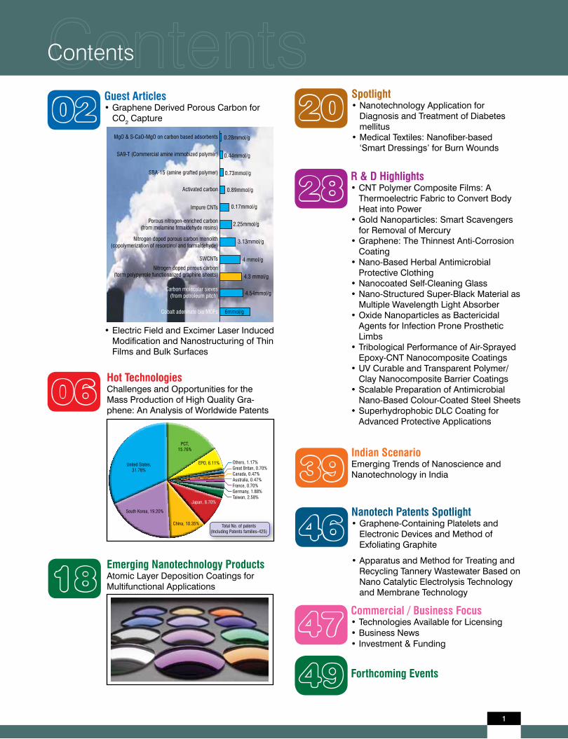
Professor Kwang S. Kim, Vimlesh Chandra and colleagues at Pohang University of Science and Technology have now synthesized a solid adsorbent made of nitrogen doped porous carbon that can selectively adsorb high concentrations of CO2 (4.3 mmolg-1 over nitrogen -0.27 mmolg-1 at 25 0C), which is several times higher than that of commercially available amine based sorbents (Fig. 1).
Studies showed that the newly developed adsorbent material, synthesized by an industrially scalable process, requires relatively less energy for recycling.
The researchers, motivated by another group that utilized the high surface area of graphene for developing a high- surface- area super capacitor material, have synthesized nitrogen doped porous
Guest Article Kwang S. Kim and Vimlesh Chandra
MgO & S-CaO-MgO on carbon based adsorbents
SA9-T (Commercial amine immobized polymer)
SBA-15 (amine grafted polymer)
0.28mmol/g
0.44mmol/g
0.73mmol/g
0.89mmol/g
0.17mmol/g
2.25mmol/g
3.13mmol/g
4 mmol/g
4.3 mmol/g
4.54mmol/g
6mmol/g
Activated carbon
Impure CNTs
SWCNTs
Porous nitrogen-enriched carbon (from melamine frmaldehyde resins)
Nitrogen doped porous carbon monolith (copolymerization of resorcinol and formaldehyde)
Nitrogen doped porous carbon (form polypyrrole functionalized graphine sheets)
Carbon molecular sieves (from petroleum pitch)
Cobalt adeninate bio MOFs
Fig. 1: Comparison of the CO2 adsorption capacity of N-doped carbon produced by chemical activation of polypyrrole functionalized graphene sheets with other conventional/ newly developed adsorbents (Image Courtesy: I. Sophia Rani, CKMNT)
3
G u e s t A r t i c l e
Kwang S. Kim and Vimlesh Chandra Center for Superfunctional Materials, Department of Chemistry, Pohang University of Science and Technology, Pohang 790-784, South Korea
Tel : +82 54-279-2110 Fax : +82 54-279-8137
E-mail: [email protected], [email protected]
carbon material with high surface area using graphene/polypyrrole composites. Graphene is known for its very high surface area (SSA of 2630 m2/g) and polypyrrole, a nitrogen-rich polymer precursor, is known for its basic nature and thermal stability. The small surface area and the high cost of polypyrrole have constrained its use as a CO2 adsorbent at the industrial level. By interfacing polypyrrole with graphene, the researchers have increased the surface area of polypyrrole by growing the material over the surface of graphene. This was done by polymerizing pyrrole in the presence of graphene oxide, followed by reduction and chemical activation at temperatures between 400 0C-700 0C under appropriate conditions. When the activation temperature was in the range of 500-600 0C, a nitrogen doped highly porous carbon (pore sizes < 2 nm) material with high surface area (1360-1588 m2/g) could be obtained through this simple process. The introduction of nitrogen in the porous carbon structure enhances its interaction with CO2 (as the band gap reduces and electrons acquire increased mobility to adsorb acidic gas) while the high-surface area,
Direct polymerization: Polypyrrole (granulated appearance)Pyrrole
Graphene Oxide Polypyrrole- graphene hybrid (Sheet-like appearance)
Chemical activation at 600 0C generated
porosity, inset: HRTEMFig. 2: SEM image of polypyrrole grown on graphene shows morphology similar to graphene sheets (not like granules of polypyrrole)
which could be achieved with the aid of graphene, enhances the area of exposure of the flue gas to this CO2 adsorbent. The adsorbent shows a very small adsorption capacity for nitrogen (0. 27 mmolg-1 at 25 0C) and hence is a promising candidate for the selective absorption of CO2 from atmospheric gases as well.
The high adsorption capacity, selectivity for CO2 capture and easy recyclability of this novel adsorbent material, and the simplicity of this scalable-production process can offer an economical solution for large-scale fossil fuel power generation plants and other coal-based industries to reduce their CO2 emissions.
Photocatalytic Cement: Green Self-Cleaning Technology to Combat Environmental PollutionAir pollution is one of the major environmental issues in present times and demands targeted and long-lasting solutions to combat with. A wide variety of products have been developed to provide effective industrialized solutions to this problem, among in which photocatalytic concrete could be a potential candidate for the construction industry. Recently, Italcementi Group, Italy has developed a potent technology named TX Active® that facilitates the manufacture of special cement products having photocatalytic activities. Based on the formulation, the photocatalytic cement may show two kinds of properties: self-cleaning, or pollution reducing, or both. These products incorporate photoactive titanium dioxide (TiO2) nanoparticles and are capable of decomposing inorganic and organic toxic substances present in the polluted air. As TiO2 pigments are inert, non-toxic and non-flammable, they are a suitable choice for being incorporated into the cement. As per a recent research finding, in Milan, approximately 15% of building surfaces in a specified area, which had been incorporated with TX Active® products, led to 50% a reduction in pollution levels.
This innovative technology was originally developed by CTG (Centro Tecnico di Gruppo, a part of Italcementi Group) and now has been certified by various research centers like ARPA and CNR. TX Active® products were first used to produce the precast panels of Misericordia Church, Rome and now have been used worldwide.
Source: www.italcementigroup.com
NANO NEWS

4
The development of non-lithographic techniques for realizing nanostructured thin
films and bulk surfaces for application in devices is a major area of current interest1-5. Such techniques have a lot of promise for the fabrication of nanoparticle arrays, nanowires and nanodots and other “nano-forms”. The effects, in each case, can be localised by an intelligent choice of process parameters, making them very attractive for niche applications. Examples of these approaches include electric field and excimer laser induced modification of thin film and bulk surfaces2-5. An additional area of interest is the development of techniques that will cause modification at specific locations on thin films and/or bulk surfaces without affecting neighbouring areas.
In the electric field induced surface modification experiment an electric field of strength 0.1 to 3.5 kV/cm is applied to an already deposited film on a substrate as shown in Fig. 1.
The pre-condition for realizing any surface modification using this technique is that the surface (thin film or bulk) should be conducting.
These are (1) grain growth (2) alignment of grains along the direction of the applied field and (3) crystallization of the films. Each of these has a threshold energy above which the effects are evident. The process of grain growth has the lowest threshold followed by that for the alignment of grains and the highest being the threshold for
V
Film
Substrate
Fig. 1: Schematic view of the electric field induced thin film surface modification experiment
Morphological reconstruction, crystallization and physical property changes can then be achieved by an optimal combination of probe separation, field strength, direction and duration.
In general, there are three effects of the applied electric field on the films.
0
0.0 49.21
02
2
6
6
8
8
10
[µm
]
[µm]
[nm]
10
4
4
(b)
[µm]
[µm
]
00
1
1
2
2
3
3
4
4(a)
Fig. 2: Atomic force microscope image of 50 nm Ni film: (a) as-deposited, (b) after electric field treatment and (c) x-ray diffraction patterns of the films
[111
]
Inte
nsity
(arb
. Uni
ts) (c)
(b)
(a)
1
2
3
40 50 60 70 80 90 100 110
(c)
2 (degree)
0.0
0.0
0.5
0.5
1.0
1.0
1.5
1.52.0
2.0(µm)
(a)
0.0
0.0
0.5
0.5
1.0
1.0
1.5
1.52.0
2.0(µm)
(b)
Si [3
11]
Inte
nsity
(arb
. Uni
ts)
Unfocussed 0.25 J/cm2 1000s
Unfocussed 0.2 J/cm2 1000s
Unfocussed 0.1 J/cm2 1000s
Silicon subs
40 50 60 70 80 90 1002 (degree)
(c)
Fig. 3: AFM of the (a) as-received Si single crystal, (b) the surface in (a) showing the formation of nanodots and (c) nanocrystallization after laser treatment.
crystallization of the films. The origin of these thresholds can be traced to the thermodynamics of surfaces under the influence of the electric field. Essentially grain growth is due to the lowering of the surface diffusion barriers in the presence of the electric field and crystallization is due to joule heating in the presence of the field. While the morphological changes are local in nature, the crystallization is a volume effect. Typical examples of the effect of
Electric Field and Excimer Laser Induced Modification and Nanostructuring of Thin Films and Bulk SurfacesGuest Article M. Ghanashyam Krishna
5
energy density along with the other control parameters can then be optimized to realize the desired modification of the surface. In a typical example, a single crystal Si surface was modified to realize a pattern of nanodots achieve photoluminescence from the surface. The effects of laser irradiation a Si single crystal surface are shown in Fig. 3. The technique has also been demonstrated on bulk surfaces of graphite and alumina, in addition to thin films of Ni, In, Au and Si.
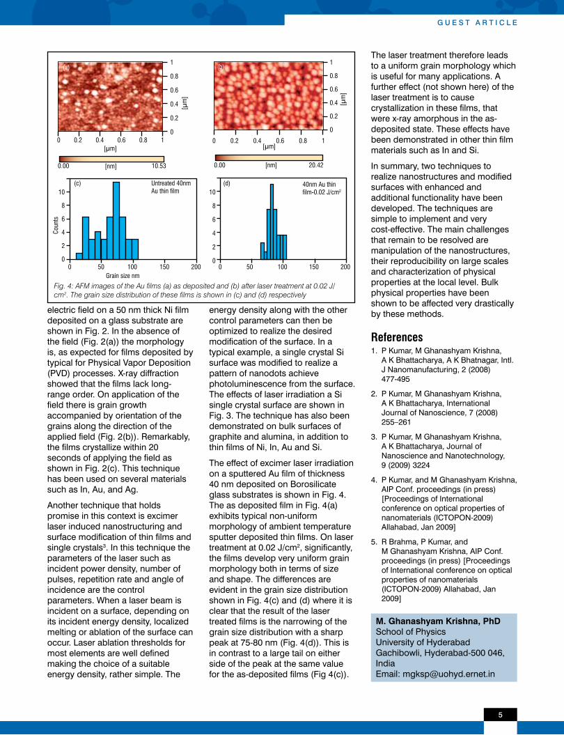
The effect of excimer laser irradiation on a sputtered Au film of thickness 40 nm deposited on Borosilicate glass substrates is shown in Fig. 4. The as deposited film in Fig. 4(a) exhibits typical non-uniform morphology of ambient temperature sputter deposited thin films. On laser treatment at 0.02 J/cm2, significantly, the films develop very uniform grain morphology both in terms of size and shape. The differences are evident in the grain size distribution shown in Fig. 4(c) and (d) where it is clear that the result of the laser treated films is the narrowing of the grain size distribution with a sharp peak at 75-80 nm (Fig. 4(d)). This is in contrast to a large tail on either side of the peak at the same value for the as-deposited films (Fig 4(c)).
The laser treatment therefore leads to a uniform grain morphology which is useful for many applications. A further effect (not shown here) of the laser treatment is to cause crystallization in these films, that were x-ray amorphous in the as-deposited state. These effects have been demonstrated in other thin film materials such as In and Si.
In summary, two techniques to realize nanostructures and modified surfaces with enhanced and additional functionality have been developed. The techniques are simple to implement and very cost-effective. The main challenges that remain to be resolved are manipulation of the nanostructures, their reproducibility on large scales and characterization of physical properties at the local level. Bulk physical properties have been shown to be affected very drastically by these methods.
References1. P Kumar, M Ghanashyam Krishna,
A K Bhattacharya, A K Bhatnagar, Intl. J Nanomanufacturing, 2 (2008) 477-495
2. P Kumar, M Ghanashyam Krishna, A K Bhattacharya, International Journal of Nanoscience, 7 (2008) 255–261
3. P Kumar, M Ghanashyam Krishna, A K Bhattacharya, Journal of Nanoscience and Nanotechnology, 9 (2009) 3224
4. P Kumar, and M Ghanashyam Krishna, AIP Conf. proceedings (in press) [Proceedings of International conference on optical properties of nanomaterials (ICTOPON-2009) Allahabad, Jan 2009]
5. R Brahma, P Kumar, and M Ghanashyam Krishna, AIP Conf. proceedings (in press) [Proceedings of International conference on optical properties of nanomaterials (ICTOPON-2009) Allahabad, Jan 2009]
00
0.2
0.2
0.4
0.4
0.6
0.6
0.8
0.8
1
1
[µm]
[µm
]
0.00 10.53[nm]
(a)
0
0
0.2
0.2
0.4
0.4
0.6
0.6
0.8
0.8
1
1
[µm
]
0.00 20.42[nm]
[µm]
(b)
Grain size nm
Coun
ts
Untreated 40nm Au thin film
00
20015010050
2
4
6
8
10(c) 40nm Au thin
film-0.02 J/cm2
00 200150100
2
4
6
8
10
50
(d)
Fig. 4: AFM images of the Au films (a) as deposited and (b) after laser treatment at 0.02 J/cm2. The grain size distribution of these films is shown in (c) and (d) respectively
M. Ghanashyam Krishna, PhD School of Physics University of Hyderabad Gachibowli, Hyderabad-500 046, India Email: [email protected]
G u e s t A r t i c l e
electric field on a 50 nm thick Ni film deposited on a glass substrate are shown in Fig. 2. In the absence of the field (Fig. 2(a)) the morphology is, as expected for films deposited by typical for Physical Vapor Deposition (PVD) processes. X-ray diffraction showed that the films lack long-range order. On application of the field there is grain growth accompanied by orientation of the grains along the direction of the applied field (Fig. 2(b)). Remarkably, the films crystallize within 20 seconds of applying the field as shown in Fig. 2(c). This technique has been used on several materials such as In, Au, and Ag.
Another technique that holds promise in this context is excimer laser induced nanostructuring and surface modification of thin films and single crystals3. In this technique the parameters of the laser such as incident power density, number of pulses, repetition rate and angle of incidence are the control parameters. When a laser beam is incident on a surface, depending on its incident energy density, localized melting or ablation of the surface can occur. Laser ablation thresholds for most elements are well defined making the choice of a suitable energy density, rather simple. The

6
Graphene Synthesis Methods
Micromechanical Exfoliation Flakes (5 to 100μm)
Small Scale Production High Cost
High Quality Uneven Films
Research Purpose
Epitaxial Growth on SiC Thin films (>50 μm)
Low Yield High Cost
High Quality High Process
Temperature (15000C) Very Expensive Substrate
Transistors Circuits
Interconnects Memory
Semiconductors
CVD (on, Ni, Cu, Co)
Thin films (≤
75 cm)
Moderate Scalability
High Cost
High Quality
High Process
Temparature
(>1000 oC)
Touch Screens
Smart W
indows
Flexible LCDs &
OLEDs
Solar Cells
Liquid Phase Exfoliation
Nanosheets (nm to a few μm
)
High Scalability
Low Yield
Moderate Quality
Low Cost
Impure
Polymer Fillers
Transparant Electrodes
Conductive Paints
Sensors
Mod
erate
Sca
libilit
y
High
Yiel
d Hi
gh Q
uality
Poten
tially
Low
Cos
tInte
rcon
nect
s FE
Ts
NEM
s Co
mpo
sites
Chem
ical
Red
uctio
n of
Gra
phite
Oxid
e
Nano
flake
s/Po
wder
(nm
to a
few μm
)
High
Sca
labilit
y Lo
w Co
st Lo
w Pu
rity
High
Def
ect D
ensit
yPo
lymer
Fill
ers
Batte
ry E
lect
rode
s
Supe
rcap
acito
rs
Cond
uctiv
e In
ks &
Pai
nts
Sens
ors
Carb
on N
anot
ube
Unzip
ping
Nano
ribbo
ns (f
ew m
icron
s)
Hot Technologies
Challenges and Opportunities for the Mass Production of High Quality Graphene: An Analysis of Worldwide PatentsIntroductionGraphene, the youngest member of the nanocarbon family, is a single layer of sp2- bonded carbon atoms arranged in a honeycomb shaped, hexagonal lattice. In 2010, Andre Geim and Konstantin Novoselov won the Nobel Prize in Physics for their groundbreaking research on isolating graphene from graphite that comes from the lead of a humble pencil. The discovery of graphene created a tidal wave of interest in this “Wonder Material” of the 21st Century. The epoch making successive discoveries of fullerene, carbon nanotube, and now graphene epitomizes the dawn of a new era of carbon.
Graphene possesses a number of extraordinary mechanical, electrical, thermal, optical and electronic properties, and therefore, holds enormous potential for profoundly transforming the next generation technologies, including computer chips, mobile phones, internet, electronic gadgets, flexible displays, solar cells,
structural composites and so on and so forth. Its fascinating attributes have triggered an avalanche of research publications and patent filings. The industry, private investors and governments, are providing substantial funding in graphene research and innovation, which will help in accelerating the pace of its commercialization. USA, European countries, Korea, Japan and other Asian countries are investing a large amount of financial capital. It is expected that the market for graphene would grow by leaps and bounds in the coming decade. According to the latest report “Graphene: Technologies, Applications and Markets” released by BCC the global graphene market
is projected to grow to $67 million in 2015 and $675.1 by 2020 at a Compound Average Annual Growth Rate (CAGR) of 58.7% within a period of 5 years. Another report entitled "world market for graphene to 2017" by the future markets, Inc. 2011 estimates that the production volume of graphene in 2010 was 28 tonnes and is projected to grow to 573 Tonnes-2017.
Graphene is undoubtedly emerging as the most promising nanomaterial because of its unique combination of superb properties, which opens a way for its exploitation in a wide spectrum of applications. However, it has to overcome a number of obstacles before we can realize its full potential for practical applications. One of the greatest challenges being faced today in
commercializing graphene is how to produce high quality
material, on a large scale at low cost, and in a
reproducible manner. The quality of graphene
plays a crucial role as the presence of defects, impurities, grain boundaries,
multiple domains, structural disorders, wrinkles in the
graphene sheet can have an
adverse effect on its electronic and
optical properties. In electronic applications,
the major bottleneck is the requirement of large
size samples, which is possible only in the case of
CVD process, but it is difficult to produce high quality and
single crystalline graphene thin films possessing very high electrical and thermal conductivities along with excellent optical transparency.
Fig. 1 A shematic showing the conventional methods commonly used for the synthesis of graphene along with their key features, the current and future applications

7
Another issue of concern in the synthesis of graphene by conventional methods involves the use of toxic chemicals and these methods usually result in the generation hazardous waste and poisonous gases. Therefore, there is a need to develop green methods to produce graphene by following environmentally friendly approaches. The preparation methods for graphene should also allow for in-situ fabrication and integration of graphene-based devices with complex architecture that would enable eliminating the multi step and laborious fabrication methods at a lower production cost.
The major hurdle in manufacturing graphene on an industrial scale is the process complexity and the associated high cost of its production, which results in expensive product. For example, currently, the selling prices of 50x50 monolayer graphene thin films by Graphene Square are $263 and $819 on Cu foil and PET thin film, respectively. Graphene nanoplatelets (5-8 nm thick) manufactured by XG Sciences is sold at about $219-229/ kg. The high cost of graphene is one of the major obstacles to its widespread adoption for commercial applications.
In the present article, an attempt has been made to carry out an extensive survey and analysis of global patents
pertaining to the various processes of graphene synthesis. The article initially summarizes the current status of the conventional approaches for the synthesis of graphene based on the survey of literature. There are several good reviews available on the subject (1-7)
and the interested readers may like to refer to the same for obtaining further details. The article particularly focuses on large-scale production methods for making high quality graphene.
Currently, the most common techniques available for the production of graphene are shown schematically in Fig. 1, which includes micromechanical cleavage, chemical vapour deposition, epitaxial growth on SiC substrates, chemical reduction of exfoliated graphene
Name of search
Area of search Keywords Time line(INPADOC Families)
String-1 Claims title and abstract
method, manufacturing, making, preparation, process, synthesis
2000- 2011 29518
String-2 Claims title and abstract
graphene, grafenol, graphén, graphene, graphitic platelets, graphitic ribbon, graphitic flakes, graphitic sheet
2000-2011 3817
String-3 Full text scotch-tape, scotch tape, electrochemical intercalation electrochemical synthesis, electrochemical deposition, graphite exfoliation,chemical vapour deposition, CVD, mechanical exfoliation, mechanical milling, mechanical shearing, mechanical cleavage, self assembling, chemical reduction, micromechanical cleavage, arc discharge, chemical reduction, unzipping of carbon nanotubes, scission of carbon nanotubes, graphite oxide reduction, vapour phase epitaxy, silicon sublimation, epitaxial growth, MBE, physical vapor deposition, PVD, molecular-beam epitaxy, pyrolysis, ion implantation, chemical synthesis, electroplating deposition
2000-2011 26236
Final String-1 and string-2 and string-3 2000-2011 1520
oxide, liquid phase exfoliation of graphite and unzipping of carbon nanotubes. However, each of the above methods can have its own advantages as well as limitations depending on its target application(s) as depicted in Fig. 1. In order to surmount these barriers in commercializing graphene, concerted efforts are being made by researchers at various R&D institutes, universities and companies from all over the globe to develop new methods for large scale production of low-cost and high quality graphene via simple and eco-friendly approaches.
Patent analysisThe present study has been conducted to provide an overview of the current patent landscape of the
10
140
160
120
100
80
60
40
20
02001 2002 2003 2004 2005 2006
Publication Year
Num
ber o
f pat
ents
2007 2008 2009 2010 2011
3 0 1 4 0 5
21
59
141
Fig. 2: Annual growth of patents related to graphene synthesis
Table 1- The search string used for carrying out the patent analysis for the graphene synthesis techniques
h o t t e c h n o l o G i e s

8
Assi
gnee
s
Academic/Research Institute Samsung Group
Research Collaborations Guardian Industries Corp
Hitachi Ltd Nanotek Instruments Inc
Hewlett-Packard Development Company L.P Fujitsu Ltd
International Business Machines Corp Northrop Grumman Systems Corporation
Mitsubishi Gas Chemical Company GM Global Technology Operations Inc
Vorbeck Materials Corp Independent Inventors
Others
Number of patents0 20 40 60 80 100 120
3030
2222333345
1316
117
Fig. 4: Assignee-wise segmentation of patents related to graphene synthesis
graphene production methods with a view to assess the future directions for an early commercialization of graphene technology.
A comprehensive patent search was carried out with different synonyms of graphene in combination with a variety of synthesis techniques coupled with appropriate truncations and proximities. The search strings as shown in Table 1 were used for carrying out the patent search in the present case. The search was based on Thomson Innovation database8, and it resulted in 1520 retrieved patents. Among these, only 234 patents were found to be relevant to the subject matter, and hence only these were considered for in-depth analysis.
Growth in PatentsFig. 2 Shows the historical worldwide patent publication trend in the area of graphene synthesis. As can be noted, there has been a rapid growth in patent publication activity since 2009, which highlights the increasing commercial potential of graphene production technologies.
Fig. 3 shows the Worldwide distribution of patenting activity related to graphene preparation methods, which indicates that USA is the world leader in this area. The
United States, 31.76%
PCT, 15.76%
EPO, 6.11%
South Korea, 19.20%
China, 10.35%
Japan, 8.70%
Taiwan, 2.58%Germany, 1.88%
France, 0.70%
Australia, 0.47%Canada, 0.47%Great Britan, 0.70%
Others, 1.17%
Fig. 3: Woredwide distribution of graphene synthesis patents (including PCT and EPO)
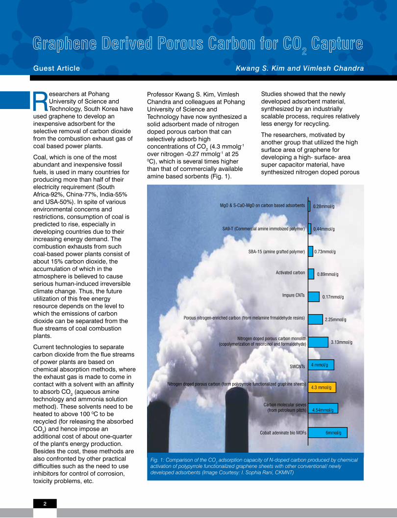
maximum numbers of patents (135, 31.76%) have been filed from the USA, followed by South Korea (82 patents, 19.20%), China (44 patents, 10.35%), Japan (37 patents, 8.70%) and Europe (26 patents, 6.11%). It is of interest to note that about half of the total number of patents were filed through Patent Cooperation Treaty (PCT) and USPTO, which clearly signifies the importance of this technology for commercial exploitation on a global scale.
Assignee AnalysisEfforts have been made to identify the key players actively pursuing R&D activity in the rapidly emerging area of graphene synthesis. As shown in the bar chart of Fig. 4, the
analysis reveals that academic/research institutes from all over the globe are doing a significant amount of research and hold the lion’s share of patents (117 patents), i.e. about 50% of the total patents filed worldwide. The second category among the assignees leading the patenting activity is independent inventors (30 patents), out of which, Jang Bor Z from Wright State University has filed 25 patents. Fig. 4 also shows that Samsung Group is the world leader with 16 patents to its credit followed by a number of companies, including Guardian Industries Corp., Hitachi Ltd., Nanotek Instruments, Hewlett Packard Development Co., L.P., Fujitsu Ltd., IBM Corp etc.
In view of the major intellectual property (I.P) contributions made by the academic/research institutes to the field of graphene synthesis, it would be pertinent to take a closer look at their role in this activity.
The number of patents owned by the top ten academic/research institutes is given in the bar chart of Fig. 5, and it is evident that Seoul National University followed by Sunngkyunkwan University (SKKU), both from South Korea are the most active assignees with 7 and 5 patents to their credit, respectively. Other active assignees are University of Texas (5 patents), Rice University (4 patents) and University of California (4 patents) all from USA. Other major players in this category are Chinese Academy of Sciences- Institute of Chemistry, China, Korea
Total No. of patents (Including Patents families-425)
n A n o t e c h i n s i G h t s

9
0 1 2 3
3
3
3
3
3
4
4
4
5
5
5
6 7
7
Number of patents
Seoul National University
Sunngkyunkwan University (SKKU)
University of Texas
Rice University
University of California
Chinese Academy of Sci., Inst of Chem.
Korea Adv Inst Sci&Tech (KAIST)
United States Department of Energy
Chonnam National University
University of Ulsan
Assi
gnee
s
Fig. 5: Number of patents related to graphene synthesis for the top 10 academic/research institutes
Advanced Institute of Science and Technology (KAIST), Korea, US Department of Energy, USA, Chonnam National University and Kyung Hee University, Korea. It is noteworthy that among the top ten, six universities belong to South Korea alone.
Industry- Institute CollaborationAlthough graphene is still in an embryonic stage, it is anticipated to have vast potential for future generations of electronic devices, advanced batteries, supercapacitors, multifunctional composites and so on. In view of the commercial importance of graphene, a number of universities/institutes are collaborating with industry, particularly from South Korea and USA. The multinational companies are funding the university research through industrial sponsorship. These industry-university collaborations would help in translating the promising research results into marketable products. Samsung Electronics Corp., a multinational player from South Korea is taking a major lead in collaborating with a few academic institutions, including Sungkyunkwan University (SKKU), Hanyang University and Leyland Stanford Jr. University, USA.
The most successful example of these collaborative efforts is the prototype development of a flexible large size (63cm) transparent touch screen made with graphene. This development is the outcome of joint efforts between Samsung and SKKU
and represents a major milestone in commercialization of graphene for electronics application. The striking feature of this technology is an innovative manufacturing approach involving growth of graphene film by Chemical Vapor Deposition (CVD) technique on a large size copper foil followed by a novel method of roll-to-roll transfer and chemical doping to produce flexible transparent electrodes suitable for OLED display and solar cell applications. The focus of the cooperation between Samsung and Hanyang University is also to develop flexible transparent electrodes via CVD process.
Samsung and Leyland Stanford Jr. University are jointly working on the development of graphene based electronic devices such as Field Effect Transistors (FETs) by using Molecular Beam Epitaxy (MBE). It is important to note that Samsung is jointly holding the patent rights with the above universities.
As discussed in the introduction, there are a number of conventional techniques available for the preparation of graphene. The ultimate choice of the technique would depend on the property requirements and the form of graphene (i.e., whether it is nanoplatelet or thin film or nanoribbon etc.) suitable for the targeted application. In general, CVD and epitaxial growth are the preferred methods for the manufacturing of high-value electronic and optoelectronic devices, where large areas and high
quality thin films with high electrical and thermal conductivities along with excellent optical transparency are the prime requirements. In the case of low-end applications such as fillers for plastics, conductive inks and paints, the quality of graphene may not be a major issue, but the availability of large quantities of material in the form of nanoplatelets/flakes/powder at an affordable price is an essential requirement. In such a case, thermal decomposition of intercalated graphite would be a suitable approach. For the applications such as electrodes for batteries or supercapacitors, sensors etc., moderate purity graphene flakes would be the right candidate, where methods like liquid phase exfoliation of graphite or chemical reduction of graphene oxide could be used.
Graphene Synthesis MethodsIn view of the immense potential of graphene for commercial and strategic applications, scientists from all over the world are intensively pursuing research and development activities to develop a variety of techniques for its synthesis, as evidenced by the large number of scientific publications and patents that have appeared in recent years. Of course, the focus has been on large-scale production of high quality graphene at low cost. Currently, innumerable techniques are available for the preparation of graphene. However, one can broadly classify them into two main categories, i.e. Bottom-up (e.g., CVD, epitaxial growth on SiC, arc discharge, chemical synthesis etc.) and Top-down (e.g., exfoliation methods) processes.
Patenting Trends of Preparation MethodsSynthesis of graphene has been classified according to the techniques employed by analysing the filed, published and granted patents. Based on this analysis (Fig. 6) it is quite evident that substantial patenting activity is directed towards the development of CVD (90 patents) and exfoliation (92 patents)
h o t t e c h n o l o G i e s

10
CVD, 90
Exfoliation methods, 92
Molecular Beam Epitaxy, 1
Laser irradiation, 2
Pyrolysis, 3
Arc Discharge, 3
Lithography, 3
Self assembly, 3
Electrically-assisted synthesis, 4
Ion implantation, 5
CNT unzipping, 6
Chemical synthesis, 6
Epitaxial growth, 17
Fig. 6: Segmentation of graphene synthesis methods
Assignees
Synt
hesis
Met
hods
Num
ber o
f pat
ents
CVDExfoliation methods
Chemical SynthesisUnzipping of CNT
LithographyEpitaxial growth
Arc dischargeSelf assembly
Laser irradiationIon implantation
Electrically-assisted synthesis
Academic/Research Institutes
Independent investors
Samsung Group
Research Collaborations
Guardian Industries Corp.
Fujitsu Ltd.
Hitachi Ltd.
Hewlett-Packard Development Company L.P
International Business Machines Corp.
Northrop Grumman Systems Corporation
Nanotek Instruments Inc.
GM Global Technology Operations Inc.
Vorbeck Materials Corp.
Mitsubishi Gas Chemical Company
Others
PyrolysisMolecular Beam Epitaxy0
1
1
1
13
3
2
8 3
54
3
14
25
4247
74 3 4 2 1 2 7
8
2232131
61
1
11 1 1
1
1 2
2
2
5101520253035404550
Fig. 7: Segmentation of patents related to synthesis methods and the assignees
techniques. Although it is not shown in the pie chart of Fig. 6, it may be noted that exfoliation methods mainly include 1) mechanical exfoliation of graphite, 2) liquid phase exfoliation of graphite and 3) chemical exfoliation of graphite oxide. Other dominant techniques are epitaxial growth on SiC substrates (17 patents), chemical synthesis (6 patents) and unzipping of carbon nanotubes (6 patents). All the above mentioned methods have significant potential for scaled-up production of graphene at an affordable cost. The pie chart also shows other emerging techniques like ion implantation, electrochemical deposition, arc discharge, self assembly, laser irradiation etc.
The data was analysed and is presented as a three-dimensional graph in Fig. 7 for each of the top patent assignees against the synthesis methods. It is interesting to note that most of the multinational corporations such as Samsung Group, IBM, Hitachi Ltd. etc. are following the CVD approach to develop high-end electronic or optoelectronic products based on high quality large area graphene thin films. In contrast, the start-up companies such as Nanotech Instruments (Angstron Materials), XG Sciences, Vorbeck Materials Corp. are directing their efforts towards developing processing routes like exfoliation, chemical synthesis, etc.
for the large scale production of graphene nanoplatelets used for low-end products, e.g., fillers for plastics, battery and supercapacitor electrodes, conductive inks and coatings etc. Academic/research institutes are focussing on developing diverse approaches like electrochemical exfoliation, microwave-assisted synthesis, liquid phase exfoliation, chemical synthesis, CVD and so forth. Some of the key players making significant
contributions to this research field are Seoul National University and Korea Institute of Science and Technology (CVD), University of Ulsan, Chonnam National University (Exfoliation technique); Beijing Institute of Technology and Institute of Physics, Chinese Academy of Sciences (Epitaxial growth); National Nanomaterials and University of Idaho (Chemical synthesis); Stanford Junior University and Rice University (Unzipping of CNTs) and so on.
Innovative Approaches for the Large Scale Production of High Quality Graphene As we have discussed earlier, graphene offers numerous opportunities for commercial exploitation because of its limitless potential for applications such as ultra strong and tough composites, touch screens, energy storage, ultra- fast transistors and so on. However, to realize its true potential for real life applications one needs to produce it in large quantities at an affordable cost, and depending on each application one has to tailor it in a suitable form and required quality. In order to meet these
n A n o t e c h i n s i G h t s
11
challenges, all-out efforts are being made by the worldwide scientific community to develop innovative approaches for the production of graphene. Some of the emerging routes for the synthesis of graphene along with the active players are introduced below.
Chemical Vapor Deposition (CVD) for Electronic and Optoelectronic DevicesGraphene is an ideal candidate for the manufacture of the next generation miniaturised, lightweight, ultra-fast and high frequency electronic and optoelectronic devices. The quality of the graphene is of paramount importance for these applications and for this purpose one has to produce large area graphene monolayer or few layer thin films of ultimate purity, large domain size, and uniform thickness. Moreover, the material should be free of any defects, grain boundaries, structural disorder, and wrinkles. CVD route has the potential to produce graphene thin films to meet these stringent requirements. The other requirement is that one should be able to produce it on a large scale by adopting continuous production process. Table 2 presents various innovative approaches along with key features, end product, targeted application(s) and assignee/active player to produce graphene thin films. Some of the notable achievements are shown in Table 2, which include roll-to-roll continuous production of graphene thin films for transparent electrodes, synthesis of single crystalline continuous thin films of graphene on liquid copper surfaces and low temperature CVD synthesis of transfer-free graphene films. Other important inventions are, the fabrication of single crystalline graphene arrays (WO2012051182A2), large area synthesis of high-quality graphene films on copper foils9, substrate-free gas phase synthesis of graphene sheets by microwave plasma CVD process (US20100301212A1) etc. Recently, scientists from National Institute of Advanced Industrial Science and Technology, Japan developed a low temperature
(300-400 0C) surface wave plasma chemical vapour deposition (SWP-CVD) technique10 to synthesize graphene-based conductive films, which are ideally suited for the fabrication of touch panels. The process is capable of producing large-area graphene-based films with excellent optical and electrical properties and is suitable for industrial scale automated manufacturing processes for various applications.
Table. 2: Emerging CVD Techniques for the Synthesis of Graphene Thin Films
Production Method: Fabrication process involving ambient pressure (CVD) on polycrystalline Ni films, to produce large area films of single/ few-layer graphene film followed by their transfer to a wide variety of substrates like SiO2/Si or SiO2 etc.
Assignee (Spin-off / licensee company): MIT, USA
Key Features: Large area graphene films (single or few layer) with uniform thickness and good mechanical stability on any type of substrate
End Product: Graphene film
Targeted Application(s): Transparent electrode, transistor device, optical detector, interconnect, on-chip capacitor etc.
Reference: US20100021708A1
Production Method: Roll-to-roll production and chemical doping of essentially single layer graphene films grown by CVD onto flexible copper substrates
Assignee (Spin-off / licensee company): Sungkyunkwan University Foundation for Corporate Collaboration, Korea
Key Features: Continuous and large scale production of graphene film for transparent electrodes of superior quality as compared to commercial ITO electrodes
End Product: Monolayer graphene film
Targeted Application(s): Graphene electrodes for touch screen
Reference: WO2011046415A2
Production Method: Epitaxial growth of graphene on single crystal Ru ( 0001) substrate
Assignee (Spin-off / licensee company): Brookhaven Science Associates, LLC
Key Features: Structurally perfect
Production Method: CVD process involving sodium ethoxide solution in ethanol
Assignee (Spin-off / licensee company): Durham University (Durham Graphene Science Ltd (DGS)), UK
Key Features: A simple and scalable process capable of depositing graphene films on non-metal substrates
End Product: Few-layer graphene platelets and thin films
Targeted Application(s): Composite materials, Batteries, capacitors, sensors etc.
Reference: WO2011012874A1
Production Method: Process for producing ripple-formed graphene sheet
Assignee (Spin-off / licensee company): Samsung Techwin Co., Ltd, and SKKU, Korea
Key Features: Forms deformation-capable graphene sheet that prevents or suppresses changes in electrical resistance when subjected to mechanical deformation
End Product: Graphene sheet containing periodic ripples
Targeted Application(s): Electronic device, sensors etc., that require flexibility
Reference: US20110171427A1
h o t t e c h n o l o G i e s
12
company): UNIST Academy-Industry Research Corporation, Korea
Key Features: The method will enable manufacturing graphene-based electronic devices with fewer steps and under less stringent conditions. It is suitable for mass production of large-area graphene films than the growth and transfer method.
End Product: Graphene layers of 1-2 nm thickness
Targeted Application(s): Flexible electronic devices and displays
Reference: WO2011111932A2
Epitaxial Graphene (EG) on SiC for Graphene-based Electronic Devices
Epitaxial Graphene has superlative electronic properties, and therefore has the potential to replace silicon for the next generation ICs and ultra-fast (100 GHz to THz frequencies) high performance electronic devices. EG is the most promising candidate for graphene-based electronics as it can be directly grown on SiC semiconductor substrate without any need for its transfer (unlike in the case of CVD graphene on metal substrates). The advantages of epitaxial growth technique are its compatibility with the present day Complementary metal–oxide–semiconductor (CMOS) technology and its scalability, which can help in realizing the ultimate dream of ushering in new era of graphene-based electronics. A few examples of emerging methods for growing superior quality mono- and few- layers epitaxial graphene on SiC are given in Table 3. These methods include sublimation of silicon at very high temperatures, confinement controlled sublimation and vapour phase epitaxy (CVD).
Table. 3: Novel Approaches for Epitaxial Growth of Graphene on SiC Substrates
Production Method: The process involves growth of graphene on
SiC surface by sublimation of silicon at temperatures above 1400 0C under controlled environment and heating cycles
Assignee (Spin-off / licensee company): R. Yakimova, M. Syvajarvi and T. Iakimov (Graphensic AB), Sweden
Key Features: It enables growth of graphene monolayer with superior quality and uniformity and suitable for large-scale production
End Product: Monolayer graphene on hexagonal silicon carbide
Targeted Application(s): Highly energy efficient white light emitting diodes for general illumination (energy savings), UV diodes (environmental cleaning sterilization and disinfection) and energy efficient and faster diodes and transistors.
Reference: WO2012036608A1
Production Method: Confinement Controlled Sublimation (CCS) to produce epitaxial graphene
Assignee (Spin-off / licensee company): Georgia Institute of Technology, USA
Key Features: The method involves encapsulation of the SiC crystals in graphite enclosures, and thereby, captures the evaporated silicon from escaping to the atmosphere and bringing growth process to equilibrium
End Product: High quality epitaxial graphene mono- and multi-layers on both the Si-face and C-face of SiC single crystals
Targeted Application(s): High-end electronic devices that operate at very high frequencies
Reference: US20090226638A1
Production Method: The method comprises vapour phase growth (CVD) of epitaxial graphene on SiC substrate that involves controlling the sublimation of silicon from the substrate by a flow of inert gas. The process also incorporates
n A n o t e c h i n s i G h t s
defect-free graphene films with single crystalline domains of linear dimensions of >200μ
End Product: 1-10 atomic layers graphene film
Targeted Application(s): Electronic devices, high quality mirrors, sensors etc.
Reference: US20100255984A1 Production Method: An innovative CVD approach to synthesize graphene flakes and continuous films on liquid copper surfaces.
Assignee (Spin-off / licensee company): Beijing National Laboratory for Molecular Sciences, CAS, China
Key Features: This unique process results in the formation of single-layered, large size (~10,000 µm2), monocrystalline hexagonal graphene flakes as well as continuous films on liquid copper surfaces. The absence of any grain boundary on liquid copper surfaces reduces the graphene nucleation density and enables self assembly of single-crystalline flakes into compact and well-ordered structure. The synthesized flakes/films show high carrier mobility, good conductivity and the capacity for carrying high current density.
End Product: Monolayered, self-aligned, large size, single-domain graphene flakes and continuous films
Targeted Application(s): Electronic devices such as Field Effect Transistors etc.
Reference: Proc Natl Acad Sci U S A. 109(21) (2012) 7992-7996
Production Method: CVD technique involving diffusion-assisted technique to synthesize large area graphene films directly on SiO2/Si, plastics and glass substrate at close to room temperature (25-160 0C).
Assignee (Spin-off / licensee

13
propane, silane or other hydrocarbons
Assignee (Spin-off / licensee company): Instytut Technologii Materialow Elektronicznych, Poland
Key Features: The process enables the synthesis of high quality predetermined number of graphene layers with desired doping level. This technique enables large-scale production using commercial CVD equipment
End Product: Epitaxial graphene on SiC substrate composed of 1-100 atomic carbon atom layers
Targeted Application(s): Microelectronic applications such as high speed transistors, terahertz oscillators, gas sensors etc.
Reference: EP2392547A2
on the research carried out at the universities have led to the creation of start-up companies, which include XG Sciences, Vornbeck Materials, Angstron Materials. In a few cases, the universities and the companies carried out collaborative research jointly. As shown in Table 3, some of the key developments are microwave-assisted exfoliation technique, intercalation and exfoliation of graphite flakes with the aid of gases, mechanical exfoliation technique for the large scale production of graphene nanoflakes by controlled ball milling of graphite flakes in a liquid medium or continuous rubbing of solid graphite block against rotating glass substrates in a solvent while simultaneously subjecting it to ultrasonication treatment. Another important development in this area is the advent of rod-coating (Meyer rod-coating) technique12 for the industrial-scale production of reduced-graphene oxide-based (RGO) flexible transparent conducting films for touch screen applications. This novel strategy follows a solution-processing approach that combines the rod–coating technique with a newly developed room temperature reduction method13 to fabricate a large-scale and uniform RGO film directly on PET and Si substrates. The attractive feature of the new process is its potential suitability for the roll-to-roll manufacturing of RGO films for flexible electronic devices.
Table. 4: Exfoliation Methods for Large Scale Production of Graphene
Exfoliation MethodsAs we have pointed out earlier, graphene has vast potential for applications such as polymer composites, conductive coatings and inks, fuel cells batteries, catalysts and ultracapacitors because of its unique combination of very high strength and stiffness, and excellent electrical and thermal conductivities. These applications require huge quantities of graphene in the form of nanosheets, nanoparticles or nanoplatelets at a reasonable cost; however, purity is not the major issue in this case. Therefore, economically viable processes for its mass production have to be developed. The projected cost of nanographene in the near future is about US $ 11/kg11 and if this goal really could be achieved then it would even compete with CNTs in the markets for composites, conductive coatings, and others. Exfoliation techniques have the potential for the large scale production of low cost nanographene. Table 4 summarizes some of the important exfoliation routes recently developed to produce nanographene on a large scale. It is interesting to note that some of these developments based
Production Method: Microwave- or radiofrequency-assisted exfoliation of intercalated graphite
Assignee (Spin-off / licensee company): Board of Trustees of Michigan State University (XG Sciences), USA
Key Features: Rapid and low cost process for converting intercalated graphite into graphene nanoplatelets; promising route for the mass production of graphene nanoscale platelets; inexpensive
alternative to carbon nanotubes for various applications.
End Product: Graphite nanoplatelets
Targeted Application(s): Composte materials, catalyst supports, battery and fuel cell electrode coatings, conductive inks, barriers for fuel tanks, RFI shielding for cables, conductive composites for ESD application, EMI shielding, electrostatic painting
Reference: US20060241237A1
Production Method: Thermal expansion of graphene oxide followed by mechanical separation
Assignee (Spin-off / licensee company): The Trustees Of Princeton University, (Vorbeck Materials). USA
Key Features: Produces multifunctional filler that improves the mechanical properties, thermal and electrical donductivities, and gas barrier properties of composites and formulations.
End Product: Functionalized graphene nanosheet (80%)
Targeted Application(s): Conductive inks and coatings for printed electronics, composite reinforcement, electrodes for next generation batteries
Reference: US7658901B2
Production Method: The process consists of wet ball milling for the exfoliation of graphite flakes in a suitable organic solvent such as N,N-dimethylformamide (DMF). The ball milling balls are coated with soft polymer that reduces damage to the graphite structure from repeated impacts during the milling process
Assignee (Spin-off / licensee company): Fujian Kaili Special Graphic C, Huaqiao University and Xiamen Knano Graphene Technology, China
Key Features: It is a low-cost
h o t t e c h n o l o G i e s
14
process amenable to large scale production. It uses inexpensive graphite powder as a feedstock
End Product: A mixture of single- and few-layer graphenes with a thickness < 3 layers
Targeted Application(s): Nanocomposites for multifunctional applications, conductive coatings, conductive inks, electrodes for batteries and supercapacitors, applications requiring EMI, ESD and RFI shielding
Reference: WO2011054305A1
Production Method: The synthesis of graphene in a liquid medium comprises continuous rubbing of a solid graphite rod/block against substrates like glass, polymers, ceramics etc. while subjecting the medium to ultrasonication.
Assignee (Spin-off / licensee company): French National Center for Scientific Research- University of Strasbourg, France
Key Features: A simple low-cost process for the preparation of graphene with high yield and is amenable to large-scale production.
End Product: A few layer graphene flakes (1-10 layers) having lateral dimensions of a few µm
Targeted Application(s): Preparation of the dispersion of graphene nanoflakes in a liquid medium
Reference: WO2011055039A1
Production Method: Intercalation of graphite flakes with environmentally friendly gases at high atmospheric pressure and suitable temperature followed by exfoliation process to yield graphene nanoplatelets
Assignee (Spin-off / licensee company): Nanotek Instruments, Inc. (Wright State University), USA
Key Features: An economical and mass production process (synthesis of graphene up to 0.1 kg)
End Product: Graphene nanoplatelets. Each platelet contains about 1-20 graphene layers
Targeted Application(s): Multifunctional composites and coatings, lithium-ion batteries and fuel cells
Reference: US7785492B1
Production Method: The synthesis route involves oxidising graphite by reacting it with hydrogen peroxide and subjecting it to microwave radiation followed by ultrasonication treatment
Assignee (Spin-off / licensee company): Chonnam National University
Key Features: A green process involving the use of environmentally friendly hydrogen peroxide instead of aggressive oxidants like H2SO4/KMnO4, formic acid etc. The process is suitable for large scale production of graphene at low cost. It is a simple process that requires short processing times.
End Product: Graphene nanosheets
Targeted Application(s): Composte materials, conductive coatings, battery electrodes etc.
Reference: WO2011083896A1
Production Method: High-throughput solution processing of large-scale graphene
Assignee (Spin-off / licensee company): The Regents of the University of California, USA
Key Features: The process consists of reducing graphite oxide paper in pure hydrazine solution to produce single layer graphene sheets over Si/SiO2 wafers.
End Product: Large area (20 X 40 µm) graphene sheets
Targeted Application(s): A wide variety of applications such as FETs, batteries, composite materials, radar absorbent materials, sensors, LEDs, display device etc.
Reference: US20100273060A1
Chemical Synthesis Methods for the Preparation of GrapheneThe bottom-up chemical synthesis routes have the potential for large-scale production of graphene at an affordable cost and may lead to a paradigm shift in this field. A number of patents related to graphene chemical synthesis methods have been filed (JP2009062241A, KR2010108106A, WO2011017338A2, CN101462719A, US20110201739A1, WO2009029984A1 and US20120068124A1). A simple solvothermal reduction approach developed by Choucair et al. (WO2009029984A1) has been a major breakthrough for low-cost, facile and large-scale production of graphene from non-graphitic materials (Table 5). This discovery has provided an impetus for the large-scale production of inexpensive graphene, and therefore has the potential to provide commercialization opportunities for real-world applications. New-south Innovations Pty Limited is seeking industry partners to further support the research and advance the proof of concept for this process technology and/or its applications14. Recently, Singh et al15 have developed an improved solvothermal process for the mass production of high-quality few-layer graphene. This commercially viable process represents a major advance in graphene solvothermal production technology. The salient features of this process are:
1. It is a safer process as it uses chemically non-explosive sodium borohydride instead of sodium metal that causes violent chemical reaction.
n A n o t e c h i n s i G h t s

15
2. The process does not require any post pyrolysis of reaction product in the high-pressure reactor unlike the method reported by Choucair et al., and thereby, reduces processing time considerably.
3. In contrast to the previously reported method, this technique utilizes surfactant during the reaction to achieve higher yield and uniform dispersion of graphene.
Another attractive option is to utilize greenhouse pollutant gases and naturally occurring and recyclable minerals to produce high quality graphene on a commercial scale. One such type of process has been developed by Graphene Technologies (High Temperature Physics, LLC), USA (Table 4). This bottom-up process is capable of producing high-quality, < 500nm lateral dimensions, one to few layer graphene nano-sheets. The company is planning to launch graphene and intermediate products under the brand name GraphenXTM. The most appealing feature of this process is that it utilizes low cost, widely available carbon dioxide gas (a major pollutant causing climate change) or other carbon bearing materials as a feedstock. It gainfully utilizes a highly exothermic reaction occurring between magnesium and CO2, and thereby, substantially reduces the energy requirement for the production of graphene. The other advantage of this process is that along with graphene it also produces novel materials, namely MgO and magnesium aluminate spinel nanopowders as well as composites of these nanomaterials intercalcated with multiple layers of graphene. Another important aspect of this processing technology is that it recycles the important materials, including Mg feedstock and HCl employed in the separation and purification of reaction products.
Table. 5: Chemical Synthesis of Graphene from Non-graphitic Materials
of graphene by the reduction of ethanol using sodium metal followed by pyrolysis of the resulting ethoxide product that is subsequently washed with water to remove sodium salts
Assignee (Spin-off / licensee company): University of New South Wales (New-south Innovations Pty Limited, Australia)
Key Features: A bottom-up, scalable and low-cost approach to produce bulk graphene sheets from non-graphitic precursors
End Product: A single atom layer thick graphene sheets
Targeted Application(s): Composite materials, batteries, catalysts, hydrogen storage, electronic devices
Reference: WO2009029984A1
Production Method: The process involves highly exothermic oxidation-reduction reaction between CO2 gas (or carbon bearing gases) and magnesium metal resulting in graphene and magnesium oxide
Assignee (Spin-off / licensee company): High Temperature Physics, LLC (Graphene Technologies), USA
Key Features: Highly economical process for the large- scale production of nanoscale graphene. It helps in reducing greenhouse CO2 gas by converting it into high- valued graphene, and thereby, would create demand for captured CO2 and reduce the requirement for sequestration of CO2. The process also produces ultrapure nano MgO as a bye- product
End Product: Single or multilayer graphene nanosheets
Targeted Application(s): Potential applications include catalysts, semiconductors, nanofillers for plastics, hydrogen storage, etc.
Reference: US20120068124A1Production Method: The solvothermal chemical synthesis
Arc Discharge Method for the Large-Scale Low-cost Production of Graphene NanosheetsAmong the various chemical methods available for the synthesis of graphene, arc-discharge bottom-up method shows significant potential for the large-scale production of few-layered high-quality graphene nanosheets (US20110114499A, CN101993060, CN102153076). The graphene can be synthesized by direct current arc-discharge evaporation of pure graphite electrodes in a variety of gases, including H2, NH3, He, Ar, CO2 and their mixtures as well as air. The process has many advantages: the synthesized graphene is of high purity and highly crystalline in nature; it also exhibits high crystallinity and high oxidation resistance; the resulting graphene sheets can be well-dispersed in organic solvents, therefore they are quite suitable for the solution processing of flexible and conductive films; arc-discharge synthesis can also be used to synthesize graphene doped with nitrogen (CN101717083A).
It is feasible to synthesize good quality graphene sheets from graphite oxide also, and the synthesized graphene shows superior electrical conductivity and high temperature stability as compared to thermally exfoliated graphene (Table 6).
Table. 6: Arc Discharge Synthesis of Few-layered Graphene
Production Method: Hydrogen arc discharge exfoliation process for graphene synthesis from graphite oxide combined with solution phase dispersion and centrifugation
Assignee (Spin-off / licensee company): Chinese Academy of Sciences, Institute of Metal Research, China
Key Features: This low-cost method produces defect-free graphene on a large scale within a short time. The resulting product exhibits high electrical
h o t t e c h n o l o G i e s

16
conductivity and good thermal stability
End Product: Graphene nanosheets with a transparent wormlike morphology
Targeted Application(s): Potential applications include electronic devices, transparent conductive films, conductive composites, Li-ion batteries and ultracapacitors
Reference: CN101993060A
University, USA
Key Features: The process is suitable for large-scale production of ultra-high quality GNRs with smooth edges and narrow width distribution
End Product: GNRs with narrow widths (10-20 nm)
Targeted Application(s): Graphene-based Field Effect Transistors (FETs)
Reference: US20110244661A1
Production Method: The process to synthesize graphene nanoribbons by electrochemical unzipping of carbon nanotubes
Assignee (Spin-off / licensee company): Council of Scientific and Industrial Research, India
Key Features: The electrochemical approach is capable of producing high quality nanoribbons with controlled widths and fewer defects
End Product: Graphene nanoribbons
Targeted Application(s): Composites, fuel cells and Li battery electrodes
Reference: WO2012035551 A1
Synthesis of High-quality Graphene Nanoribbons (GNRs) by Unzipping of Carbon NanotubesGraphene is considered to be the strongest candidate for replacing silicon in the next generation of electronic devices, in particular ultra-fast Field-Effect Transistors (FETs) because of its very high carrier (electron/hole) mobility and quantum-hall effect. However, the absence of band-gap limits its usage in digital switching, where high value of on-off current ratio is an essential requirement. Fortunately, this limitation can be overcome by inducing quantum confinement and edge effects as in the case of narrow width graphene nanoribbons (GNRs).
For the fabrication of FETs it is absolutely necessary to obtain GNRs with controllable widths and smooth edges and the unzipping of CNTs approach enables the large-scale production of GNRs with high quality and desirable characteristics as required for device integration. Table 7 shows two promising routes for the synthesis of high quality GNRs.
Table. 7: Synthesis of High-quality GNRs by Unzipping of CNTs
Production Method: Mildly oxidized MWCNTs are subjected to unzipping process by ultrasonication in an organic solvent to produce graphene nanoribbons (GNRs)
Assignee (Spin-off / licensee company): The Board of Trustees of the Leland Stanford Junior
Environmentally Friendly Approaches for the Synthesis of High-quality GrapheneAs we have seen earlier in the Exfoliation Methods section, among various methods, chemical reduction of Graphene Oxide (GO) seems to be the most promising route because it enables large-scale production of functionalized nanographene at low-cost. Moreover, through chemical functionalization the unique electrical properties of graphene can be exploited for a wide range of electronic and optoelectronic applications. However, GO synthesized by Hummer’s or modified Hummer’s methods requires use of strong and hazardous oxidizers such as sulphuric acid potassium
permanganate etc. Moreover the reduced graphene film is prepared by subjecting GO to chemical treatments using highly toxic and unstable hydrazine, which requires utmost care. In view of this, a number of green approaches for the synthesis of graphene and GO are being developed. The present article summarises some of the eco-friendly graphene synthesis techniques in Tables 4 and 5 (US20120068124A1, WO2011083896A1, WO2011055039A1). In addition, the current status of environmentally friendly approaches for the mass production of graphene from GO have been comprehensively addressed in a recent review16. Researchers from Sichuan University, China have synthesized graphene by chemical reduction of graphite oxide using green and eco-friendly polyphenol/green tea juice as a reducing agent (CN101875491A). The process involves exfoliation of graphite oxide by subjecting it to ultrasonic treatment and then the resulting product is used to prepare graphene oxide solution in water with high dispensability, biocompatibility and good stability. This environmentally friendly method is simple, economical and suitable for large-scale production of graphene
Concluding RemarksGraphene undoubtedly is one of the shining stars in the field of nanotechnology today. Its intriguing combination of spectacular properties as well as a host of potential commercial applications have grabbed the widespread interest of scientists and engineers the world over. Graphene's potential applications are vast and ever growing. It could be put to use in super light cables (space elevator?). satellites and aircrafts; smart phones; ultra-thin flexible displays; transparent touch-screens; world’s fastest transistors, bomb detectors, and so on. But despite all such tall claims, it has yet to make in-roads into real-life applications. In order to realize its full potential for practical applications, one has to resolve the
n A n o t e c h i n s i G h t s

17
most challenging problem; economically viable mass production of high-quality graphene via environmentally friendly processes. Fortunately, it is quite evident from the foregoing discussions that this situation is about to change soon, with new innovative graphene synthesis routes appearing on the scene. The present article provides a general overview of the current and emerging approaches for the synthesis of graphene based on literature and patent analyses. It also outlines the possible directions for future research and it is hoped that future work along these lines would help in addressing these concerns to realize our dream of commercialization of graphene
References1. D. Jariwala, A. Srivastava and P. M.
Ajayan, "Graphene Synthesis and Band Gap Opening", J. Nanoscience and Nanotechnology, 11 (2011) 6621–6641
2. W.Xiangjian, Yi Huang and C.Yongsheng, “Focusing on Energy and Optoelectronic Applications: A Journey for Graphene and Graphene Oxide at Large Scale”, Accounts of Chemical Research, 45 (2012) 598-607
3. R.M. Frazier et al., “Advances in Graphene-Related Technologies: Synthesis, Devices and Outlook”, Recent Patents on Nanotechnology, 6 (2012) 79-98
4. C.Wonbong et al., “Synthesis of Graphene and Its Applications: A Review”, 35 (2010) 52-71.
5. E. D. Grayfer et al., “Graphene: chemical approaches to the synthesis and modification”, 80 (2011) 751–770
6. D.R. Dreyer, R.S. Ruoff and C.W. Bielawski, “From Conception to Realization: An Historial Account of Graphene and Some Perspectives for Its Future”, Angewandte Chemie International Edition, 49 (2010) 9336-9344.
7. Y.Zhu et al., “Graphene and Graphene Oxide: Synthesis, Properties, and Applications”, Adv. Mater., 22 (2010) 3906–3924
8. https://www.thomsoninnovation.com
9. X. Li, “Large-Area Synthesis of High-Quality and Uniform Graphene Films on Copper Foils”, Science, 324 (5932) (2009) 1312-1314
10. http://dx.doi.org/10.1063/1.3561747 ; J.Kim (JP) et al., “Manufacturing method for transparent conductive carbon film, and transparent conductive carbon film”, WO2011115197A1 (Priority Date: March- 17-2010)
11. http://nextbigfuture.com/2011/04/commercialization-of-graphene.html
12. J. Wang et al., “Rod Coating: Towards Large-Area Fabrication of Uniform Reduced Graphene Oxide Films for Flexible Touch Screens”, Advanced Materials, 24 (21) (2012) 2874-2878
13. M. Liang et al., “High-Efficiency and Room-Temperature Reduction of Graphene Oxide: A Facile Green Approach towards Flexible Graphene Films”, Small, 8 (2012) 1180–1184
14. http://unsw.technologypublisher.com/technology/2754
15. D. K. Singh, P. K. Iyer and P. K. Giri, “Improved Chemical Synthesis of Graphene Using a Safer Solvothermal Route”, International Journal of Nanoscience, 10 (1) (2011) 1-4
16. J. I. Paredes et al., “Environmentally friendly approaches toward the mass production of processable graphene from graphite oxide”, J. Mater. Chem., 21 (2011) 298-306.
h o t t e c h n o l o G i e s
Contributed by Samba Sivudu Kurva and Yashwant Mahajan, CKMNT
Open Access Journals on Nanoscience & Nanotechnology
• Nanoscale Research Letters, http://www.nanoscalereslett.com/content
• Nano Research, http://www.thenanoresearch.com/
• Nano Biomedicine and Engineering, http://www.oaso.org/nbe/index.php?journal=nbe&page=index
• Journal of Nanobiotechnology, http://www.jnanobiotechnology.com/
• International Journal of Nanomedicine, http://www.
dovepress.com/international-journal-of-nanomedicine-journal
• Nano-Micro Letters (NML), http://www.nmletters.org/index.php?journal=nml
• Nano Reviews, http://www.nano-reviews.net/index.php/nano/index
• Applied Nanoscience, http://www.springer.com/materials/nanotechnology/journal/13204
• Chinese Science Bulletin, http://csb.scichina.com:8080/kxtb/CN/volumn/index.html
• SCIENCE CHINA Chemistry, http://chem.scichina.com:8081/sciBe/EN/volumn/current.shtml
• SCIENCE CHINA Technological Sciences, http://tech.scichina.com:8082/sciEe/EN/volumn/current.shtml#
• Journal of Biomaterials and Nanobiotechnology, http://www.scirp.org/journal/jbnb
• Soft Nanoscience Letters, http://www.scirp.org/journal/snl
• World Journal of Nano Science and Engineering, http://www.scirp.org/journal/wjnse
• The Open Nanoscience Journal, www.benthamscience.com/open/tonanoj/
• Beilstein Journal of Nanotechnology, http://www.beilstein-journals.org/bjnano/home/home.htm
• Nanomaterials and Nanotechnology, http://www.intechweb.org/nanomaterials-nanotechnology-journal.html
• Nano-Micro Letters, http://nmletters.org/
• Nanotechnology, Science and Applications, http://www.dovepress.com/nanotechnology-science-and-applications-journal
• International Nano Letters, http://inljournal.com/
• The Journal of Nanomedicine and Nanotechnology, http://omicsonline.org/jnmnthome.php
• International Journal of Nano Dimension (IJND), http://ijnd.ir/
• Journal of Nano- and Electronic Physics, http://jnep.sumdu.edu.ua/en/component/main/
• Nanomaterials, http://www.mdpi.com/journal/nanomaterials
• Journal of Nanophotonics Letters, http://spie.org/x4345.xml

18
Emerging Nanotechnology Products
Atomic Layer Deposition Coatings for Multifunctional ApplicationsAtomic Layer Deposition (ALD) is a technique of applying nanoscale thin film coating on various substrates by using sequential gas phase chemical process.To initiate this process, chemicals are allowed to interact at the surface of the material in a successive manner. Its repeated exposure allows the thin film to get deposited on the surface1. ALD in combination with nanotechnology can be used to manufacture very precise nanometer–thick, pinhole–free and totally conformal thin films on any shape and geometry.
Company ProfileBeneq Oy, the Finnish company, is engaged in both manufacturing and supplying nano-coating for various industrial and research purposes. Its headquarters is based at Vantaa, Finland with various service centres
Liquid phase process (sol-gel)
Source controlled gas phase process (PVD)
Surface controlled gas phase process (ALD)
Semi-surface controlled gas phase process (CVD)
Comparison of coating thickness uniformity with other methods
Applications of Nano-Based ALD Coating Technology in Various Sectors2
Electronics Industry
Optical Industry
Medical Industry
Ald Coating Techniq
BENEQ
SERVICES
Jewelary & Minting Industry
Decorative Industry
spread across the world. Beneq applies nano-based ALD technology for its coating services. Annually, it serves over 100 customers with more than 1000 separate runs, covering a wide array of coating applications, processes and tool set-ups.
nBIOCOMPTM-ALD CoatingsnBIOCOMPTM coating has been developed as a thin film technology for bio-medical applications. nBIOCOMPTM ALD coatings enhance the resistance against corrosion and abrasion while improving the frictional characteristics of the implants. Another advantage of this film is its nanometer scale thickness, which prevents the formation of detrimental particles inside the body. This ALD can also be used to deposit low and high protein affinity coating that acts as an antimicrobial agent for various laboratory equipments, analytical devices, biochips, and other biological materials. It is better than the present conventional method because of its ability to deposit thin films with uniform thickness.
ALD coated devices for medical application
nDECOTM-ALD Coatings Color and appearance are among the most important features for the marketing of consumer products like mobile phones, sun glasses, sun films etc. nDECOTM is the commercial product of Beneq, which is used as a decorative coating for the valuable products. For this purpose, dichroic filters (interference filters) along with ALD are used to impart the color by selectively reflecting the wavelength
of desired colors, whereas conventional paints are based on the phenomenon of selective color absorption. This coating enables dark and absorptive color films, which are easy to apply and give a metal-like coating on polymers. Other important advantages of this product are as follows:
• Does not require the application of binders and solvents
• Adhesion is better than Physical Vapour Deposition (PVD) films
• Coating degradation is very less
• The metal appearance can be given to plastics
Decorative coating of lenses by ALD Technology
nOPTOTM-ALD coatingsOne of the wide applications of ALD technology is in optical and photonics industry to deposit coatings on those materials, which are difficult to coat by other conventional methods. nOPTOTM is a pinhole free coating which can be applied in nanometer scale thickness. Besides photonics, this nanocoating has several other applications in the field of engineering novel materials. This technology is useful in creating novel
Nano-Laminates
Graded structures
Tailored mixtures
Modified materials Doping, Interfaces
Thin film structure enabled by ALD technology
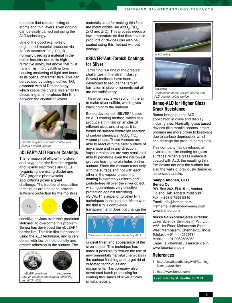
19
e m e r G i n G n A n o t e c h n o l o G y P r o d u c t s
materials that require mixing of atoms and thin layers. Even doping can be easily carried out using the ALD technology.
One of the good examples of engineered material produced via ALD is modified TiO2. TiO2 is normally used as a material in the optics industry due to its high refractive index, but above 150 OC it transforms into crystalline form causing scattering of light and loses all its optical characteristics. This can be avoided by using modified TiO2 prepared with ALD technology, which keeps the crystal size small by depositing an amorphous thin film between the crystalline layers.
nCLEAR®-ALD Barrier CoatingsThe formation of efficient moisture and oxygen barrier films for organic and flexible electronics like OLED (organic light-emitting diode) and OPV (organic photovoltaic) applications poses a great challenge. The traditional deposition techniques are unable to provide sufficient protection for the moisture
Flexible polymer substrate coated with Beneq thin film system
materials used for making thin films are metal oxides like Al2O3, TiO2, ZnO and ZrO2. This process needs a low temperature so that thermolabile products or devices can also be coated using this method without damage.
nSILVER®Anti-Tarnish Coatings for SilverTarnishing is a one of the greatest challenges in the silver industry. Several methods have been developed to reduce the tarnish formation in silver ornaments but all are not satisfactory.
The silver reacts with sulfur in the air to make silver sulfide, which gives black color to the material
Beneq developed nSILVER® based on ALD coating method, which can produce a thin film on articles of different sizes and shapes. It is based on surface controlled reaction of certain chemicals (Al2O3, TiO2) in vapour phase. These vapours are able to react with the silver surface of any shape and in any direction. Vapour molecules are very small and able to penetrate even the narrowest grooves leaving no pin-holes on the surface. Since the vapours react only with the surface and not with each other in the vapour phase, the coating is extremely uniform and pinhole-free all over the silver object, which guarantees very effective protection against tarnishing. nSILVER® is superior to other film techniques in this respect. Moreover, the thin film is completely transparent and does not change the
Beneq-ALD for Higher Glass Crack ResistanceBeneq brings out the ALD application in glass and display industry also. Normally, glass based devices (like mobile phones, smart phones) are more prone to breakage due to surface depression, which can damage the product completely.
This company has developed an invisible thin film coating for glass surfaces. When a glass surface is coated with ALD, the resulting thin film covers not only the surface but also the walls of previously damaged nano-scale cracks.
Sampo Ahonen, CEO Beneq Oy P.O. Box 262, FI-01511, Vantaa, Finland, Tel: +358 9 7599 530 Fax: +358 9 7599 5310 Email: [email protected], [email protected] www.beneq.com
Mikko Saikkonen-Sales Director Laser Science Services (I) Pvt. Ltd., #66, 1st Floor, Mahadevan Street, West Mambalam, Chennai-33, India. Telefax : +91 44 42129784 Mobile : +91 9962595852 Email: [email protected] www.laserscience.in
References1. http://en.wikipedia.org/wiki/Atomic_
layer_deposition
2. http://www.beneq.com
2Ag S Ag2S+ =
sensitive devices over their predicted lifetimes. To overcome this problem, Beneq has developed the nCLEAR® barrier film. This thin film is deposited using the ALD technique, and is very dense with low pinhole density and greater adhesion to the surface. The
nSILVER® coated coin Uncoated coinAfter 24 hours of accelerated tarnishing test (ISO 4538)
Schematic of glass strengthened by ALD
original finish and appearance of the silver object. This technique has made it possible to reduce the use of environmentally harmful chemicals in the surface finishing and to get rid of outdated techniques and equipments. This company also developed batch processing for coating thousands of silver articles simultaneously.
No ALD coating
ALD coatingComparison of non-coated device with ALD coated mobile device
Contributed by M. Kavitha, CKMNT

20
Spotlight
Brain and cerebral circulation (cerebrovascular disease)Eyes (retinopathy)
Heart and coronary circulation (coronary heart disease)
Lower limbs (peripheral vascular disease)
Diabetic foot (ulceration and amputation)
Peripheral nervous system (neuropathy)
Kidney (nephropathy)
Oral health
Source: http://www.idf.org/sites/default/files/da5/Fig%201.1%20The%20major%20diabetes%20complications.jpg
Fig. 1: Represents the clinical impacts of Diabetes mellitus
Nanotechnology Application for Diagnosis and Treatment of Diabetes mellitusDiabetes is a chronic disorder of metabolism, characterized by high levels of glucose in the body due to impaired insulin production or insulin action, or both. Diabetes comes from the Greek word meaning ‘to pass or flow through’ and mellitus
means ‘sweet’1.The major forms of the disease are type I and type II diabetes. Type I diabetes is characterized by a lack of insulin production. Type II Diabetes is caused by the body’s ineffective use of insulin. Diabetes mellitus (DM) occurs throughout the world and it is especially common (type II) in the developed countries due to their urban lifestyle and unhealthy dietary habits2. The complications (Fig.1) of DM include kidney disease, retinopathy (eye damage), nerve damage, stroke, and cardiac arrest3. According to a WHO report, the number of global DM patients was
120 million in 1994, 171 million in 2000 and may rise above 366 million by 20304. Out of these data, Type II diabetes accounts for almost 90% cases worldwide.
SymptomsDiabetes often goes undiagnosed because many of its symptoms seem to be ordinary and not special. Recent studies indicate that the early detection of symptoms can help in treatment and thus, help in reducing the complications of diabetes5.
Type I Type II
Frequent urination
Any of the Type I symptoms
Unusual thirstBlurred vision,
Frequent infections
Extreme hungerCuts/bruises are
slow to heal
Unusual weight loss
Tingling/numbness in
the hands/feet
Extreme fatigue and Irritability
Recurring skin, gum, or bladder
infections
Table: Symptoms of Type I & Type II diabetes
Mechanism of Blood Sugar Regulation and Pathophysiology of DiabetesMost of the food we eat is broken down by the digestive enzymes into a simpler sugar called glucose. After digestion, the glucose passes into the bloodstream and is made available to the body cells as the main source of energy and growth. The levels of glucose in the blood are regulated by α- cells and β- cells secreted by the Islet of Langerhans region in the pancreas. If the glucose level falls in blood (as in conditions like heavy exercise, prolonged fasting etc.), the hormone glucagon
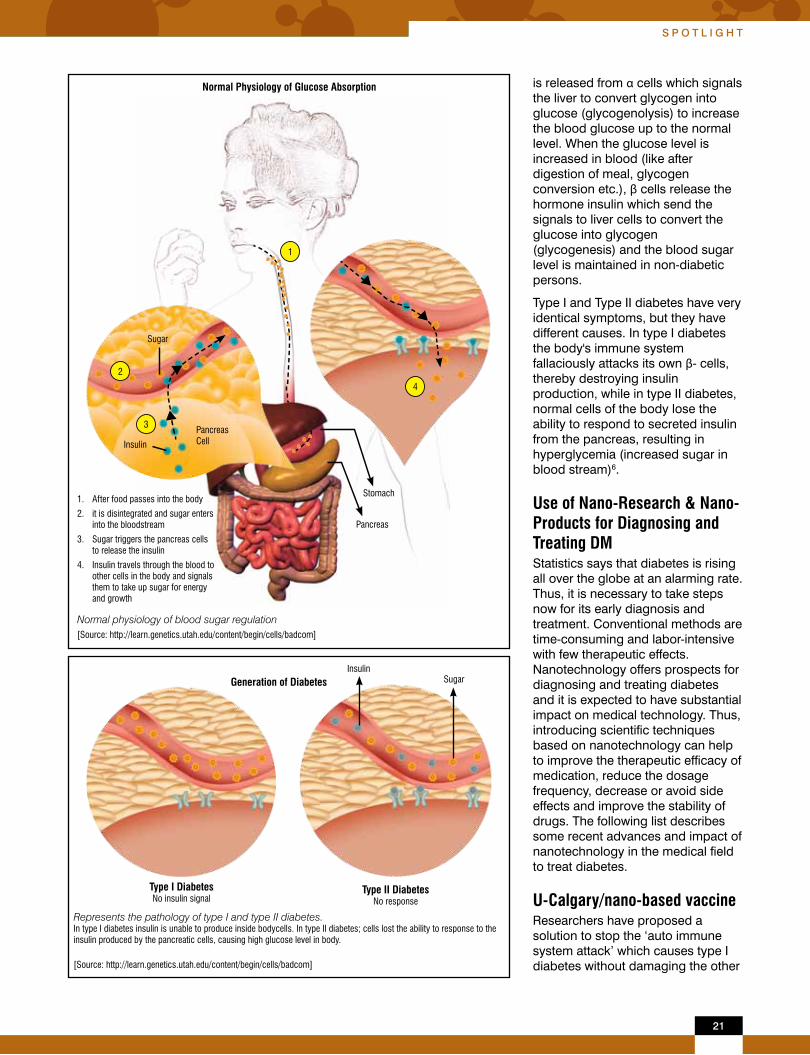
21
s P o t l i G h t
is released from α cells which signals the liver to convert glycogen into glucose (glycogenolysis) to increase the blood glucose up to the normal level. When the glucose level is increased in blood (like after digestion of meal, glycogen conversion etc.), β cells release the hormone insulin which send the signals to liver cells to convert the glucose into glycogen (glycogenesis) and the blood sugar level is maintained in non-diabetic persons.
Type I and Type II diabetes have very identical symptoms, but they have different causes. In type I diabetes the body's immune system fallaciously attacks its own β- cells, thereby destroying insulin production, while in type II diabetes, normal cells of the body lose the ability to respond to secreted insulin from the pancreas, resulting in hyperglycemia (increased sugar in blood stream)6.
Use of Nano-Research & Nano-Products for Diagnosing and Treating DMStatistics says that diabetes is rising all over the globe at an alarming rate. Thus, it is necessary to take steps now for its early diagnosis and treatment. Conventional methods are time-consuming and labor-intensive with few therapeutic effects. Nanotechnology offers prospects for diagnosing and treating diabetes and it is expected to have substantial impact on medical technology. Thus, introducing scientific techniques based on nanotechnology can help to improve the therapeutic efficacy of medication, reduce the dosage frequency, decrease or avoid side effects and improve the stability of drugs. The following list describes some recent advances and impact of nanotechnology in the medical field to treat diabetes.
U-Calgary/nano-based vaccineResearchers have proposed a solution to stop the ‘auto immune system attack’ which causes type I diabetes without damaging the other
Type I Diabetes No insulin signal
Type II Diabetes No response
InsulinSugar
Represents the pathology of type I and type II diabetes.In type I diabetes insulin is unable to produce inside bodycells. In type II diabetes; cells lost the ability to response to the insulin produced by the pancreatic cells, causing high glucose level in body.
Generation of Diabetes
[Source: http://learn.genetics.utah.edu/content/begin/cells/badcom]
Pancreas CellInsulin
Sugar
Stomach
Pancreas
Normal Physiology of Glucose Absorption
1
2
3
4
Normal physiology of blood sugar regulation
1. After food passes into the body
2. it is disintegrated and sugar enters into the bloodstream
3. Sugar triggers the pancreas cells to release the insulin
4. Insulin travels through the blood to other cells in the body and signals them to take up sugar for energy and growth
[Source: http://learn.genetics.utah.edu/content/begin/cells/badcom]

22
n A n o t e c h i n s i G h t s
Encapsulated Insulin
Side View
Outside View
Bound Glucose
Glucose Receptors
Glucose Receptors
Liposome
[Source: http://dev.nsta.org/evwebs/1150/futuretech.htm]
Showing the side and outer view of Nanomist
Smart Wireless Patch
Medication Pump
Monitoring the glucose level via wireless device
immune cells in the body. They have developed a nano-based vaccine which contains protein and peptide coated nanoparticles specific to type I diabetes. These nanoparticles suppress the autoimmune T-cells (which destroy beta cell mistakenly) and thus prevent the auto-immune reaction.
Source: Parvsus Therapeutics, Inc Julia McFarlane Diabetes Research Centre, the University of Calgary, Canada
http://www.sciencedirect.com/science/article/pii/S1074761310001226
Remote monitoring sensorNano sensors in the form of patches are applied to patient’s skin (with added innovative technology). This sensor will be connected to various hospital systems via a wireless network and the patient’s condition will be automatically accessed using advanced mathematical models which will provide immediate instructions with regard to the insulin therapy and possible crisis situations.
Source: Atos Origin &Reaction, Europe
http://es.atos.net/es-es
Implantable SensorThe Polyethylene glycol beads coated with fluorescent molecules are administered via intra dermal route (which passes in to the blood stream and stays in the interstitial fluid). Whenever the glucose level is decreased in interstitial fluid, beads produce fluorescence which can be traced by IR radiation.
Source: Draper Lab Cambridge, MA Headquarters
http://www.draper.com/contact_us.html
Smart insulinResearchers have chemically engineered insulin to act as a self-regulating delivery system. This smart insulin detects the high glucose level in the blood and
releases the insulin in appropriate manner. When the glucose level drops, the drug stabilizes and the insulin is trapped until the glucose level is increased in the blood stream.
Source: Smart Cell Inc., USA (Acquired by Merck in 2010)
http://www.merck.com/newsroom/news-release-archive/corporate/2010_1202.html
http://www.syracuse.com/news/index.ssf/2010/12/east_syracuse_minoa_graduate_s.html
GT-250 Glucose monitoring patchesGentag Inc. has developed disposable skin patches by silicon fabrication technique for monitoring the blood glucose level by the use of wireless sensor and cellphones (which is already programmed). This sensor chip technology eliminates the traditional pain and discomfort of the current finger pricking technology used by diabetic patients. This technique can be used for monitoring diabetes in both type I & II.
sustained action. It is found to be easy to use, small, reliable, safe and accurate device.
Source: Debiotech S.A. Switzerland
http://www.debiotech.com
Artificial Nano PancreasA nano-medical device (a box) contains beta pancreatic cell which is meant to be implanted beneath the skin of diabetic patients. The box contains tiny silicon material with a very specific nanopore size (20 nm in diameter) which allows insulin and glucose to pass through it while restricting the larger immune molecules. This device controls the glucose level for a restricted period of time.
Source: Mayo clinic, USA
http://www.mayoclinic.com
NanomistScientists have developed a drug component which is a combination of liposome (nano- encapsulation of insulin) and glucose receptors. Whenever blood glucose level rises, it triggers the glucose receptors and initiates the release of insulin from liposomes in nano-doses. These liposomes will work together to
Source: GENTAG, INC., Washington, DC 20007, USA
http://www.gentag.com/documents/GT250.pdf
Nanopump™This is an insulin delivering pump which is integrated with Micro-Electro Mechanical Systems (MEMS) chip which can sense the increase levels of glucose in blood and thus promote the release of insulin for

23
s P o t l i G h t
maintain a stable glucose level in the blood stream. It is administered in the form of a nasal spray. This technology has received a US patent.
Source: Patent no: US60/918,662
http://dev.nsta.org/evwebs/1150/futuretech.htm
Implantable device with silicon sealResearchers at University of British Colombia have developed an implantable device (sealed with polydimethylsiloxan membrane) with external magnetic field which delivers the drug at a controlled level for treating retinal damage caused by diabetes mellitus. It is a safe and effective dosage form with no side effects.
nano-carrier to deliver insulin by oral ingestion. Preclinical studies have shown the successful delivery of insulin loaded in biodegradable nanospheres. This sphere contains polyester and polyanhydride mixture which enables the drug to move across the gastro intestinal track thereby preventing the insulin destruction as demonstrated in a rat model.
Source: Radwant & Aboul-Enein, Saudi Arabia
DOI: 10.1080/02652040110081406
http://faculty.ksu.edu.sa/Dr_MRadwan/Documents/insulinnanoM.pdf
ConclusionApplication of nanotechnology in diabetic condition can improve drug delivery and efficacy by 1) increasing the rate to reaction of drug, 2) reducing the level of dosage, 3) decreasing the toxicity level, 4) prolonging the action of drug component and 5) minimizing the side effects. The above studies suggest that nanotechnology has considerable potential for diagnosing and treating diabetes mellitus.
References1. http://www.nevdgp.org.au/info/
careplans/diabetesCP/diabetes_whatis_diet_feet_testing.pdf
2. http://en.wikipedia.org/wiki/Diabetes_mellitus
3. http://www.emedicinehealth.com/diabetes/article_em.htm
4. http://www.who.int/diabetes/facts/world_figures/en/
5. http://www.diabetes.org/diabetes-basics/symptoms/
6. http://en.wikipedia.org/wiki/Blood_sugar_regulation
Magnetic Membrane
Deflected Membrane
Applied Magnetic Field
Drug
Drug Reservoir
Drug Formulation
Released Drug
Actuation
Aperture
The diagram represents the release of the drug from the formulation[Source: http://www.publicaffairs.ubc.ca/wp-content/uploads/2011/06/Schematic.jpg]
Source: University of British Columbia, Canada
http://pubs.rsc.org/en/Content/ArticleLanding/2011/LC/c1lc20134d
Nanospheres for oral insulinNormally insulin is taken by parenteral route (injection) because it gets degraded by intestinal pH if taken orally. To overcome this problem researchers have found a Contributed by M. Kavitha, CKMNT
No More Daily Insulin Injection for Diabetic PatientsIn India, hyperglycemia is one of the most common diseases associated with some vascular complications, and demands an effective but safe pharmaceutical agent to combat with. Recently, a team of scientists at National Institute of Immunology (NII), New Delhi, has developed a nano-based formulation of insulin molecule for treating type I diabetes. According to Dr. Avadhesh Surolia (former director, (NII)), this formulation will be helpful for insulin-dependent diabetic patients, who undergo suffering from fright and pain caused by frequent injections.
This new formulation contains nano-based oligomers of insulin hormone, where the hormone is released inside the body at regular intervals, preventing the dipping of sugar levels beyond a critical limit. This formulation needs to be injected once in a week, and eliminates the requirement of daily dosage of the insulin hormone. However, clinical trials are still going on and the product is in its conceptual stage. A US-based firm, Life Science Pharmaceuticals will work further on this product, and probably in the next couple of years; this nano-formulation will be in the market after passing clinical trials. A similar product is available in some of the European countries, which have been approved by USFDA.
Source: DNA (http://www.dnaindia.com/health/report_nano-insulin-may-relieve-diabetics-of-daily-shots_1656399-all)
NANO NEWS

24
n A n o t e c h i n s i G h t s
Medical Textiles: Nanofiber-based ‘Smart Dressings’ for Burn WoundsBurn injuries are one of the major global health problems. As per a recent report of World Health Organization (WHO), every year 195,000 people from all over the world die because of fire alone. Additionally, most of the people who survive from burn injuries carry the stigma for lifetime disabilities and deformity. Over 95% of burn-related deaths have been accounted from low-income countries as most of the high-income countries have made major advances in fire-prevention strategies and burn care. South-East Asia is on the top for fire-related deaths and also for the burn mortality rate among women1.
A burn injury may damage some or all skin layers and is caused by a hot solid, a hot liquid (scalding) or a flame (Source: International Society for Burn Injuries (ISBI)). However, injuries related to electricity, radioactivity, ultraviolet radiation, chemicals and respiratory damage due to smoking are also considered as burn injuries. There are various systems for classifying burn wounds such as:
By severity: As per this system, burn injuries can be major, moderate or minor (American Burn Association) based on various factors like patient’s age, total body surface area (TBSA) burnt and co-morbidities.
By Surface area: The “Rules of Nines” is applied to determine the burnt area where burnt body is divided into sections and each section is equal to 9% of TBSA.
By depth: Ambroise Pare, a French barber-surgeon devised this system of classification, which is based on the depth of a burn injury. As per this system burns can be divided into first, second and third/fourth degrees (Fig. 1).
Apart from breathing, pain, nutritional and circulatory maintenance, it is
extremely important to protect a burn wound from microbial infections because of low levels of cell mediated immunity and skin injury. These infections are mostly caused by fungi and bacteria like Methicillin-resistant Staphylococcus aureus (MRSA) and Pseudomonas aeruginosa (Fig. 2) which release various proteases, adhesion and colonization proteins that damage adherent tissues2.
Fig. 1: Burn degree types (a) first degree (b) second degree (superficial partial thickness) (c) second degree (deep partial thickness) (d) eight day old fourth degree burn on foot. [Images courtesy: QuinnHK, Wikimedia Commons]
(a) (b)
(d)
Fig. 2: Burn wound infection caused by Staphylococcus aureus3. [Photo Credit: Gregory Moran, M.D., Center for Disease Control and Prevention] 3
Besides cleaning the wound and applying various topical anti-microbial agents, wound dressings could be an effective solution in preventing microbial infections for burn care4. The suitability of a burn wound dressing depends on a burn type. Conventional dressings are not efficient enough to induce haemostasis (mechanism to stop bleeding), adherence and in holding a moist environment around wound5. Due to the advances in the field of nanoscience & technology, it is now possible to design Nanofiber-based Wound Dressings (NFDs), where an electrospun-nanofibrous layer is applied to a basic support fabric material. NFDs have the following advantages6, 7:
Haemostasis: Induce haemostasis due to their nanofibrous structure.
High filtration & liquid absorption efficiency: Absorb wound exudates efficiently.
(c)
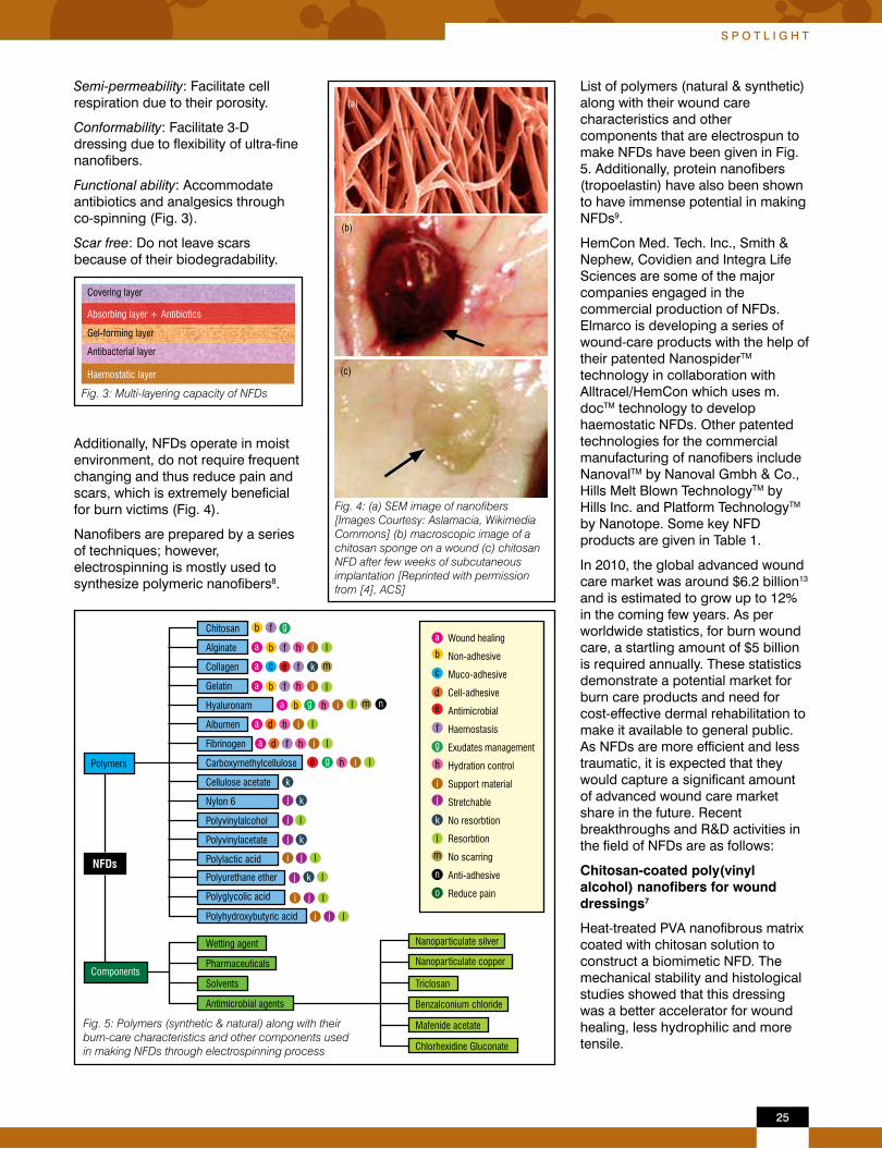
25
s P o t l i G h t
Semi-permeability: Facilitate cell respiration due to their porosity.
Conformability: Facilitate 3-D dressing due to flexibility of ultra-fine nanofibers.
Functional ability: Accommodate antibiotics and analgesics through co-spinning (Fig. 3).
Scar free: Do not leave scars because of their biodegradability.
Chitosan
Alginate
Collagen
Gelatin
Hyaluronam
Albumen
Fibrinogen
Carboxymethylcellulose
Cellulose acetate
Nylon 6
Polyvinylalcohol
Polyvinylacetate
Polyurethane ether
Polyglycolic acid
Polyhydroxybutyric acid
Nanoparticulate silverWetting agent
Pharmaceuticals
Solvents
Antimicrobial agents
Nanoparticulate copper
Triclosan
Benzalconium chloride
Mafenide acetate
Chlorhexidine Gluconate
Polylactic acid
a
a
a
a
a
a
b
b
b
b
c
e
e f
f
f
f
f
g
g
g
h
h
h
h
h
h
i
i
i
i
i
i
i
i
i
k
k
k
k
k
l
l
l
l
l
l
l
l
l
l
l
m
m
n
j
j
j
j
j
j
j
d
d
NFDs
Components
Polymers
Wound healing
Non-adhesive
Muco-adhesive
Cell-adhesive
Antimicrobial
Haemostasis
Exudates management
Hydration control
Support material
Stretchable
No resorbtion
Resorbtion
No scarring
Anti-adhesive
Reduce pain
a
b
c
e
f
g
h
i
k
l
m
n
o
j
d
Fig. 5: Polymers (synthetic & natural) along with their burn-care characteristics and other components used in making NFDs through electrospinning process
Fig. 4: (a) SEM image of nanofibers [Images Courtesy: Aslamacia, Wikimedia Commons] (b) macroscopic image of a chitosan sponge on a wound (c) chitosan NFD after few weeks of subcutaneous implantation [Reprinted with permission from [4], ACS]
Covering layer
Absorbing layer + Antibiotics
Gel-forming layer
Antibacterial layer
Haemostatic layer
Fig. 3: Multi-layering capacity of NFDs
Additionally, NFDs operate in moist environment, do not require frequent changing and thus reduce pain and scars, which is extremely beneficial for burn victims (Fig. 4).
Nanofibers are prepared by a series of techniques; however, electrospinning is mostly used to synthesize polymeric nanofibers8.
List of polymers (natural & synthetic) along with their wound care characteristics and other components that are electrospun to make NFDs have been given in Fig. 5. Additionally, protein nanofibers (tropoelastin) have also been shown to have immense potential in making NFDs9.
HemCon Med. Tech. Inc., Smith & Nephew, Covidien and Integra Life Sciences are some of the major companies engaged in the commercial production of NFDs. Elmarco is developing a series of wound-care products with the help of their patented NanospiderTM technology in collaboration with Alltracel/HemCon which uses m.docTM technology to develop haemostatic NFDs. Other patented technologies for the commercial manufacturing of nanofibers include NanovalTM by Nanoval Gmbh & Co., Hills Melt Blown TechnologyTM by Hills Inc. and Platform TechnologyTM by Nanotope. Some key NFD products are given in Table 1.
In 2010, the global advanced wound care market was around $6.2 billion13 and is estimated to grow up to 12% in the coming few years. As per worldwide statistics, for burn wound care, a startling amount of $5 billion is required annually. These statistics demonstrate a potential market for burn care products and need for cost-effective dermal rehabilitation to make it available to general public. As NFDs are more efficient and less traumatic, it is expected that they would capture a significant amount of advanced wound care market share in the future. Recent breakthroughs and R&D activities in the field of NFDs are as follows:
Chitosan-coated poly(vinyl alcohol) nanofibers for wound dressings7
Heat-treated PVA nanofibrous matrix coated with chitosan solution to construct a biomimetic NFD. The mechanical stability and histological studies showed that this dressing was a better accelerator for wound healing, less hydrophilic and more tensile.
(a)
(b)
(c)

26
n A n o t e c h i n s i G h t s
Hyperbranched polyglycerol(HPGL) NFD as drug delivery vehicle14
A nanofibrous dressing of HPGL having Calendula officinalis which is an anti-inflammatory and wound healing agent was prepared and studies showed that HPGL nanofibers could prove to have drug delivery properties when used as NFD for wound care.
SiO2 NFD with embedded silver nanoparticles as recoverable wound cover 15
Silver nanoparticles (Ag NPs) were embedded on SiO2 nanofibers and results showed that due to the conformability of SiO2 nanofibers, this dressing facilitated convenient patterning into a shape required for wound cover. Embedded Ag NPs showed a long-term antibacterial effect while inorganic part of this NFD could be recovered through calcinations without lost of any flexibility.
Degradability of collagen could be improved by combining it with zein16
Addition of zein could improve the electrospinnability of collagen while various other mechanical and in vitro degradable properties of the dressing could be regulated by altering collagen/zein blending ratio.
Nano ZnO in combination with Sodium alginate/poly(vinyl alcohol) nanofibers to enhance antibacterial property17
Presence of nano-ZnO could improve antibacterial properties of sodium alginate/PVA nano-mats especially over Escherichia coli and Staphylococcus aureus; however, optimal concentration of ZnO is yet to be formulated for providing maximum antibacterial activity with least toxicity is yet to be identified.
Regulated release of dual drugs with composite nanofibers containing drug-loaded nanoparticles18
By adjusting the preparation process of the electrospinning solution,
Product Description Manufacturer
IntegraTM
Nanofibrous bovine Type I collagen/
glycosaminoglycans/synthetic polysiloxane
based dermal analogue10
Integra Life Sciences (http://www.integralife.com)
NanocellTM Nanofibrous microbial cellulose masks
Thai Nano Cellulose (http://www.thainanocellulose.
com)
Apligraf®
Bovine collagen nanofibrous sponge
with neonatal foreskin fibroblasts and keratinocytes
Novartis (http://www.apligraf.com)
KerlixTM AMD
Nanofibrous Polyhexamethylene Biguanide (PHMB)
gauge
Kendall (http://www.kendallhq.com)
DermaFuseTM Bioactive borate glass nanofibrous dressing
Mo-Sci Corporation, U.S.A (http://www.mo-sci.com)
TransCyte®
Electrospun nylon mesh/collagen/silicone dermal
substitute embedded with allogenic fibroblasts11
Advanced Tissue Sciences (http://www.transcyte.com)
TegadermTM
Electrospun poly(caprolactone)
(PCL)/gelatine/polyurethane scaffold
3M Company (http://www.3M.com)
BiobraneTMCollagen/nylon/
silicone nanofibrous dressing12
Smith & Nephew (http://wound.smith-nephew.
com)
Dermagraft-TC®
Electrospun polyglactin having cultured neonatal
foreskin fibroblasts
Advanced Tissue Sciences, Inc. (http://www.advancedbiohealing.
com)
ChitoFlex® Fabricated chitosan nanofibrous dressing
HemCon Med. Tech. Inc. (http://www.hemcon.com)
PermacolTM Dermal matrix of porcine nanofibers
Covidien (http://www.covidien.com)
AlloDerm®Candavers acellular matrix nanofibrous
autograft
LifeCell Corporation (http://www.lifecell.com)
MyskinTMElectrospun PVC with cultured autologous
keratinocyte
Altrika Limited (http://www.altrika.com)
LaserskinTM
Nanofibrous hyaluronic acid
membrane embedded with
autologous keratinocytes
Fidia Advanced Biopolymers Ltd (http://www. fidiapharma.it)
Table 1: Key Nanofiber-based Burn Wound-Care Products

27
s P o t l i G h t
programmable release of dual drugs could be achieved through NFDs. This technique might be an effective way for an early wound healing.
Challenges and Future ProspectsAlthough modern-age NFDs are more effective than conventional dressings, they are very expensive. NFDs are extremely difficult to handle due to their delicacy and require some kind of tangible support; however, chemical properties of the support fabric make nanofiber coating heterogeneous19. In addition, nanofibers often show poor adhesion to the base support. In a recent study20, plasma-treated cotton gauzes were used as the support fabric after electrospinning chitosan nanofibers where nanofibers showed better adhesion, a low rate of degradation and moisture vapour transport (Fig. 6).
Thus a special care has to be taken in choosing a suitable combination of nanofiber and support fabric for making NFDs; however, with the recent nano-technological advancements, we can expect many more efficient NFD products in the future.
References1. http://www.who.int/violence_injury_
prevention/other_injury/burns/en
2. Ma Kun, “Biomimetic Nanofiber/stem Cell Composite for Skin Graft Application”, (2009), NUS, http://www.scholarbank.nus.edu.sg/handle/10635/16586
3. http://microbewiki.kenyon.edu/index.php/Microbial_Infection_of_Burn_Wounds
4. Victor T. Tchemtchoua et al., “Development of a Chitosan Nanofibrillar Scaffold for Skin Repair and Regeneration”, Biomacromolecules, ACS, 12 (9), (2011) 3194–3204
5. Alves Janete Lara, Bellino Nuno José, Geraldes Maria José, “Nano-Bioabsorbent Composite Wound Dressing for Exudate Management”, John Wiley & Sons, Inc., WIREs Nanomed Nanobiotechnology, (2010) 510–525
6. Zahedi et al., “A Review on Wound Dressings with an Emphasis on Electrospun Nanofibrous Polymeric Bandages”, John Wiley & Sons, Ltd., Polym. Adv. Technol., 21, (2010) 77–95
7. Kang YO et al., “Chitosan-coated Poly (vinyl alcohol) Nanofibers for Wound Dressings”, J. Biomed. Mater. Res. B. Appl. Biomater, 92 (2), (2010) 568-76
8. S Sell et al., “Extracellular Matrix Regenerated: Tissue Engineering via
Electrospun Biomimetic Nanofibers”, Society of Chemical Industry, Polym. Int., 56, (2007) 0959–8103
9. Li et al., “Electrospun protein fibers as matrices for tissue engineering”, Biomaterials, 26, (2005) 5999-6008
10. Chong Ee Jay, “Nanofibrous Mat for Tissue Engineering, Wound Dressing and Dermal Reconstitution”, (2006), NUS
11. S. P. Zhong, Y. Z. Zhang, C. T. Lim, “Tissue Scaffolds for Skin Wound Healing and Dermal Reconstruction”, John Wiley & Sons, Inc., WIREs Nanomed Nanobiotechnology, 2, (2010) 510–525
12. http://www.aetna.com/cpb/medical/data/200_299/0244.html
13. http://www.visiongain.com/Report/716/Advanced-Wound-Care-World-Market-Prospects-2011-2021
14. Vargas EA et al., “Hyperbranched Polyglycerol Electrospun Nanofibers for Wound Dressing Applications”, Acta Biomater, 6 (3), (2010) 1069-78
15. Zhijun Ma et al., “Silver Nanoparticles Decorated Flexible SiO2 Nanofibers with Long-term Antibacterial Effect as Reusable Wound Cover”, Colloids and Surfaces A: Physicochem. Eng. Aspects, 387, (2011) 57– 64
16. Jiantao Lin et al., “Co-electrospun Nanofibrous Membranes of Collagen and Zein for Wound Healing”, ACS Applied Materials & Interfaces, Article ASAP (2012)
17. Shalumon KT et al., “Sodium Alginate/poly (vinyl alcohol)/Nano ZnO Composite Nanofibers for Antibacterial Wound Dressings”, Int. J. Biol. Macromol., 49 (3), (2011) 247-54
18. Yazhou Wang et al., “Electrospun Composite Nanofibers Containing Nanoparticles for the Programmable Release of Dual Drugs”, Polymer Journal, NPG, 43, (2011) 478-483
19. Challenges in Advanced Nanofiber Wound Dressings Annual Report, NTC Project, (2009), http://www.ntcresearch.org/projectapp/?project=F09-NS06
20. Marian McCord, “Challenges in Advanced Nanofiber Wound Dressings, Annual Report, October 2010”, NTC Project: F09-NS06, http://www.ntcresearch.org/pdf-rpts/AnRp10/F09-NS06-A10.pdf
Fig. 6: Better adhesion of nanofibers on plasma-treated cotton gauzes, sample (b) & (c) show better adhesion up to 53% and 24% respectively20.
(a) (b)
(c)
Contributed by Abhilasha Verma, CKMNT

28
R & D Highlights
CNT Polymer Composite Films: A Thermoelectric Fabric to Convert Body Heat into PowerThermoelectric (TE) devices are solid state devices with small size and light weight, which convert a flow of heat into electrical energy, and can make a significant contribution in the future by thermoelectric waste heat recovery for a wide range of applications such as power generation and refrigeration, while reducing the fossil fuel consumption and global warming. The energy conversion efficiency of TE devices mostly depends on the figure-of-merit (Z = α2σ/κ) or the dimensionless figure-of-merit (ZT) of TE materials, which relates to the material parameters such as Seebeck coefficient (α), electrical conductivity (σ), and thermal conductivity (κ). Among the vast number of inorganic TE materials, bismuth telluride (Bi2Te3) based materials have been employed as efficient TE materials over the last few years due to their excellent TE performance with maximum ZT values (≈ 1) at room temperature. However, the applications of Bi2Te3 –based TE devices are limited for large-scale energy conversion due to their high cost, shortage of materials and toxicity. Recent advances in organic polymers have emerged as alternative TE materials due to their attractive properties like light weight, low thermal conductivity and ease of processing on large areas. As they have low electrical conductivities, many researches have been carried out to improve the conversion efficiency of organic polymers by incorporating suitable dopants,
which can enhance their electrical transport properties.
Organic TEs such as carbon nanotube (CNT)/polymer composite thin films are recognized as potential TEs that exhibit several benefits due to their ordered structure, which increases ZT by improving both Seebeck coefficient and electrical conductivity. In the present study, Hewitt and his group from Wake Forest University, North Carolina, have developed a TE module in which multiple layers of individual CNT films were stacked up in flexible plastic, Polyvinylidene fluoride (PVDF). When, they were bonded together by pressing the multilayered film, the melting point of plastic resulted in a felt like thermoelectric fabric, where the thermoelectric voltage was equal to the sum of contributions from each layer in the fabric (Fig. 1). Currently, the best CNT/polymer TE shows a low ZT ≈ 0.02 and a power factor of 25 μWm K−2, whereas Bi2Te3 TE shows a ZT ≈ 1 and a power factor of 7800 μWm−1 K−2. However, both CNT/polymer and Bi2Te3 TEs show low thermal conductivities, which allow to
maintain the temperature difference across the film. The power per unit mass for Bi2Te3 is about 232 mWg−1, while current CNT/polymer films have a power per unit mass of 60 mWg−1, although the potential of CNT/polymer TEs may reach as high as 1300 mWg−1, if a ZT ≈ 0.2 is reached. However, the power output could be potentially optimized by improving the Seebeck coefficient through chemical treatment of the CNTs, increasing electrical conductivity by using conducting polymers or decreasing thermal conductivity by introducing phonon scattering defects along the CNTs and by adding more CNT layers, which makes them even thinner.
CNT/polymer films are potentially cheaper, lighter and more easily processed and eco-friendly in comparison to commercial Bi2Te3TE materials. Results suggest that CNT/polymer films could replace the commercial TEs for use in lightweight, flexible, and portable consumer electronics such as wrapping around a flashlight, powering a weather radio, and charging a prepaid cell phone. CNT/
(a) (b)
(c)
10mm
h
e
h
e
h
eI
TnTc
A
B
C
D
E
+VTEP
-
Fig. 1: (a) Layer arrangement for the multilayered fabric. CNT/PVDF conduction layers (B, D) are alternated between PVDF insulation layers (A, C, E). Every first conduction layer contains p-type CNTs (B), while the second contain n-type CNTs (D). Layers A−D can be repeated to reach the desired number of conduction layers (N). When the film is exposed to a temperature gradient (ΔT), charge carriers (holes (h), or electrons (e-)) migrate from Th to Tc resulting in a thermoelectric current (I). (b) The resulting thermoelectric voltage (VTEP) can be read across the ends of the first and last conduction layers. (c) The thermoelectric fabric remains flexible and lightweight.

29
polymer TE films with suitable dimensions and multilayer inter-fabric contacts with appropriate layer count could be used as inside lining in a thermoelectric jacket in the near future that gathers warmth from the body heat, while exterior remains cold from the outside temperature.
Source: Corey A. Hewitt et al., “Multilayered Carbon Nanotube/Polymer Composite Based Thermoelectric Fabrics”, Nano Lett., 12 (3), (2012) 1307-1310, doi: 10.1021/nl203806q
Gold Nanoparticles: Smart Scavengers for Removal of Mercury
Mercury is a well known toxic and harmful pollutant, present in the environment, which can have harmful effects on living organisms due to its bioaccumulation tendency even at low doses. Fish and other wildlife in various ecosystems commonly attain mercury levels of toxicological concern through mercury-containing emissions from human-related activities such as mining, pharmaceutical and pesticide products and processing and refining of mercury ores. Consumption of such contaminated fish and other animal products can cause severe health disorders such as memory loss, neuronal damage, infertility, as well as birth defects in infants.
Several investigators have found that most of the water sources such as nutrient-poor lakes, streams, wet-lands, reservoirs, and often very remote areas are contaminated with mercury (Hg (II)), where fish commonly contain high levels of mercury. Other challenges such as extended droughts, population growth, and increasing groundwater pollution also reduce the accessible supply of freshwater, thus limiting the availability of potable water. Presently, adsorption, ion- exchange, amalgamation and chemical precipitations of mercury are the technologies available to remove mercury from contaminated water; however, they are often costly and time-consuming. Hence, there is a growing demand to develop new purification methods to improve the availability of fresh water.
Advances in nanoscience and engineering may provide new opportunities to develop cost-effective and eco-friendly purification processes to remove toxic soft metals such as Hg, Ag, Pb, Cd, and Tl from water. Nanoparticles (NPs) are effective absorbent materials due to their attractive physicochemical properties like reduced size, higher surface area, high adsorption capacity, and their ability to functionalize with many surfactants that enhances their affinity towards target molecules. Also, the Brownian dispersion of NPs of very small diameter enables them to stay suspended and allows the particles to spread through large volumes of water without using any external
agitation methods. Usually, mercury is used to extract gold from its ore by the reaction of mercury with gold, forming an alloy, i.e. gold amalgam; consequently, researchers have employed the reverse of this approach to remove mercury from contaminated water using gold nanoparticles.
Recently, Issac Ojea-Jimenez and his group have established a new process to eliminate Hg (II) ions by employing sodium citrate coated Au NPs as a catalyst, while avoiding the use of NaBH4, a toxic and strong reducing agent. The Hg (II) was eliminated through search, reduce and trap from water by growing as non-spherical coalescent NPs with increasing size (Fig. 1). Since sodium citrate acts as both coating and soft reducing agent, it enhanced the dispersion of Au NPs and reduced Hg (II) ions to elemental mercury before their interaction with Au NPs. The catalytic ability of Au NPs to eliminate Hg (II) was established by various techniques, which implied the interaction between Au NPs and Hg by reduction, precipitation on the surface of the Au NPs and the consequent metal inter-diffusion and alloying, where the available surface decreased till reaction stops.
The process could successfully reduce the amount of Hg (II) in drinking water up to 1-5 ppb, the safe level set by World Health Organization (WHO). Though gold is expensive, the good elimination ratio and easy recovery of gold by exposing the amalgam to high pressure or temperature make this process viable, especially in closed environments such as waste water treatment plants. As Au NPs can scan quickly through larger volumes of water than their larger micro-sized counterparts, the present method can also be implemented for purifying flowing water.
Source: Issac Ojea-Jimenez et al., “Citrate-Coated Gold Nanoparticles as Smart Scavengers for Hg (II) Removal from Polluted Waters”, ACS Nano, 6 (3), (2012) 2253-2260, doi: 10.1021/nn204313a
Fig. 1: Removal of Hg from the Ebro River: (a) precipitate resulting from the treatment of 6.5 ppm Hg (II) with Au NPs (1.7 nM Au NPs, 7.1 ppm Au) in Ebro River water (41% elimination) and (b) optical microscope image of the precipitate taken at 40× magnification and zoom.
(a) (b)
r & d h i G h l i G h t s
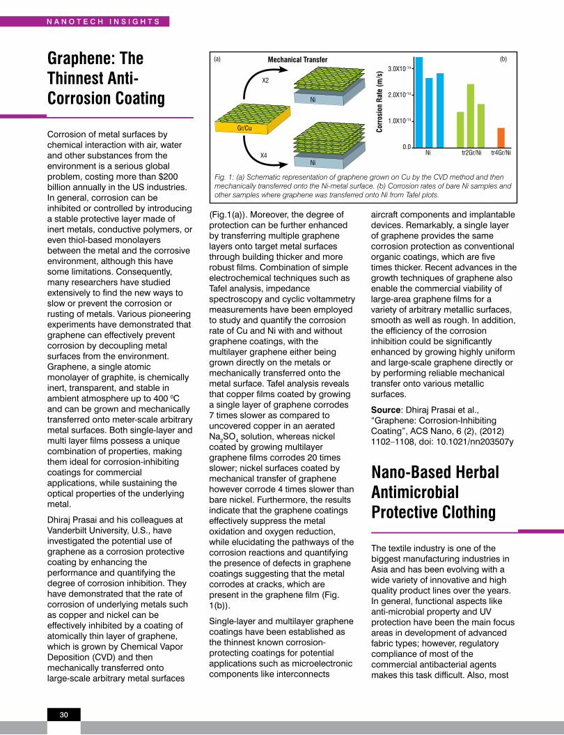
30
n A n o t e c h i n s i G h t s
Graphene: The Thinnest Anti-Corrosion Coating
Corrosion of metal surfaces by chemical interaction with air, water and other substances from the environment is a serious global problem, costing more than $200 billion annually in the US industries. In general, corrosion can be inhibited or controlled by introducing a stable protective layer made of inert metals, conductive polymers, or even thiol-based monolayers between the metal and the corrosive environment, although this have some limitations. Consequently, many researchers have studied extensively to find the new ways to slow or prevent the corrosion or rusting of metals. Various pioneering experiments have demonstrated that graphene can effectively prevent corrosion by decoupling metal surfaces from the environment. Graphene, a single atomic monolayer of graphite, is chemically inert, transparent, and stable in ambient atmosphere up to 400 0C and can be grown and mechanically transferred onto meter-scale arbitrary metal surfaces. Both single-layer and multi layer films possess a unique combination of properties, making them ideal for corrosion-inhibiting coatings for commercial applications, while sustaining the optical properties of the underlying metal.
Dhiraj Prasai and his colleagues at Vanderbilt University, U.S., have investigated the potential use of graphene as a corrosion protective coating by enhancing the performance and quantifying the degree of corrosion inhibition. They have demonstrated that the rate of corrosion of underlying metals such as copper and nickel can be effectively inhibited by a coating of atomically thin layer of graphene, which is grown by Chemical Vapor Deposition (CVD) and then mechanically transferred onto large-scale arbitrary metal surfaces
Nano-Based Herbal Antimicrobial Protective Clothing
The textile industry is one of the biggest manufacturing industries in Asia and has been evolving with a wide variety of innovative and high quality product lines over the years. In general, functional aspects like anti-microbial property and UV protection have been the main focus areas in development of advanced fabric types; however, regulatory compliance of most of the commercial antibacterial agents makes this task difficult. Also, most
(Fig.1(a)). Moreover, the degree of protection can be further enhanced by transferring multiple graphene layers onto target metal surfaces through building thicker and more robust films. Combination of simple electrochemical techniques such as Tafel analysis, impedance spectroscopy and cyclic voltammetry measurements have been employed to study and quantify the corrosion rate of Cu and Ni with and without graphene coatings, with the multilayer graphene either being grown directly on the metals or mechanically transferred onto the metal surface. Tafel analysis reveals that copper films coated by growing a single layer of graphene corrodes 7 times slower as compared to uncovered copper in an aerated Na2SO4 solution, whereas nickel coated by growing multilayer graphene films corrodes 20 times slower; nickel surfaces coated by mechanical transfer of graphene however corrode 4 times slower than bare nickel. Furthermore, the results indicate that the graphene coatings effectively suppress the metal oxidation and oxygen reduction, while elucidating the pathways of the corrosion reactions and quantifying the presence of defects in graphene coatings suggesting that the metal corrodes at cracks, which are present in the graphene film (Fig. 1(b)).
Single-layer and multilayer graphene coatings have been established as the thinnest known corrosion-protecting coatings for potential applications such as microelectronic components like interconnects
aircraft components and implantable devices. Remarkably, a single layer of graphene provides the same corrosion protection as conventional organic coatings, which are five times thicker. Recent advances in the growth techniques of graphene also enable the commercial viability of large-area graphene films for a variety of arbitrary metallic surfaces, smooth as well as rough. In addition, the efficiency of the corrosion inhibition could be significantly enhanced by growing highly uniform and large-scale graphene directly or by performing reliable mechanical transfer onto various metallic surfaces.
Source: Dhiraj Prasai et al., “Graphene: Corrosion-Inhibiting Coating”, ACS Nano, 6 (2), (2012) 1102–1108, doi: 10.1021/nn203507y
3.0X10⁻¹⁴
Ni tr2Gr/Ni
Corr
osio
n Ra
te (m
/s)
tr4Gr/Ni
2.0X10⁻¹⁴
1.0X10⁻¹⁴
0.0
X2
X4
Gr/Cu
Ni
Ni
Mechanical Transfer
Fig. 1: (a) Schematic representation of graphene grown on Cu by the CVD method and then mechanically transferred onto the Ni-metal surface. (b) Corrosion rates of bare Ni samples and other samples where graphene was transferred onto Ni from Tafel plots.
(a) (b)
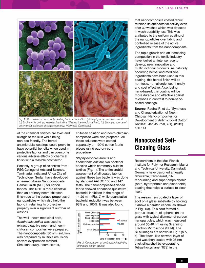
31
r & d h i G h l i G h t s
of the chemical finishes are toxic and allergic to the skin while being non-eco-friendly. The herbal antimicrobial coatings could prove to have potential benefits when used in protective fabrics and can overcome various adverse effects of chemical finish with a feasible cost factor.
Recently, a group of scientists from PSG College of Arts and Science, Tamilnadu, India and Africa City of Technology, Sudan have developed a neem-chitosan Nanocomposite Herbal Finish (NHF) for cotton fabrics. This NHF is more effective than an ordinary neem-chitosan finish due to the surface properties of nanoparticles which also help the fabric in retaining its protective property over a significant number of washes.
The well known medicinal herb, Azadirachta indica was used to extract bioactive neem and neem-chitosan composites were prepared. The nanocomposite (30 nm) solution was prepared by multiple emulsion/solvent evaporation method. Simultaneously, neem extract,
chitosan solution and neem-chitosan composite were also prepared. All these solutions were coated separately on 100% cotton fabric pieces using pad-dry-cure procedure.
Staphylococcus aureus and Escherichia coli are two bacterial species which commonly exist in textiles (Fig. 1). The antimicrobial assessment of all coated fabrics against these two bacteria was done by standard AATCC 100 and 147 tests. The nanocomposite-finished fabric showed enhanced qualitative bacterial inhibition in the range of 14-20 mm (Fig. 2) while quantitative bacterial reduction was between 93% and 100%. It was also found
Fig. 1: The two most commonly existing bacteria in textiles: (a) Staphylococcus aureus and (b) Escherichia coli. (c) Azadirachta indica (Neem), the medicinal herb, (d) Shrimps, source of commercial chitosan. [Images courtesy: Wikimedia Commons]
(a) (b)
(c) (d)
that nanocomposite coated fabric retained its antibacterial activity even after 30 washes which was detected in wash durability test. This was attributed to the uniform coating of the nanoparticles over fabric and controlled release of the active ingredients from the nanocomposite.
The rapid growth and an increasing competition in the textile industry have fuelled an intense race to develop new, innovative and multifunctional products. As naturally occurring herbal and medicinal ingredients have been used in this coating, this herbal finish will be non-toxic, non-allergic, eco-friendly and cost effective. Also, being nano-based, this coating will be more durable and effective against microbes in contrast to non-nano-based coatings.
Source: Radhai R. et al., “Synthesis and Characterization of Neem Chitosan Nanocomposites for Development of Antimicrobial Cotton Textiles”, Jeff Journal, 7(1), (2012) 136-141
Fig. 2: Comparison of antibacterial activities of treated cotton fabrics
Nanocoated Self-Cleaning Glass
Researchers at the Max Planck Institute for Polymer Research, Mainz and Technical University, Darmstadt, Germany have designed an easily fabricable, transparent, oil-rebounding and super-amphiphobic (both, hydrophobic and oleophobic) coating that helps a surface to clean itself.
The researchers coated a layer of soot on a glass substrate by holding it above a paraffin candle, as shown in Fig. 1(a). This soot formed a porous structure of spheres on the glass with typical diameter of carbon nanoparticles, which was measured around 30-40 nm using Scanning Electron Microscope (SEM). The SEM images are shown in Fig. 1(b & c). The fractal-like network layer of soot was then coated with 25 nm thick silica shell by evaporating Tetraethoxysilane (TES) in the
Neem Chitosan nanocompositeNeem Chitosan
compositeChitosan solution
Zone of inhibition (nm)
Antib
acte
rial a
gent
use
d
S.aureusE.coli
Neem extract
0 10 20 30

32
Nano-Structured Super-Black Material as Multiple Wavelength Light Absorber
A perfect black material in general has the potential for absorbing all colour of light falling on its surface at any angle without reflecting any of them. Scientists intended to have an ideal black material with zero reflectance for various space related applications and also in the field of electronics and solar energy, but had been unsuccessful so far.
n A n o t e c h i n s i G h t s
presence of ammonia as a catalyst using Chemical Vapour Deposition (CVD) method. The thickness of the silica shell was controlled by varying the duration of the CVD process.
After calcining hybrid carbon/silica network at 600 0C, the soot was decomposed, leaving intact the roughness and network texture of the layer making the black coating transparent. The next step included deposition of fluorinated silane onto the hollow silica structure through CVD process. After silanization, the coating was found to be super-amphiphobic in nature; this property was demonstrated by wetting the surface using water and other alkanes. The static contact and the roll angle for water droplets were found to be 1650 and 10, respectively and for organic liquid droplets they were found to be 1540 to 1620 and 50 respectively. Due to low adhesion of the coating with water and other alkanes, the droplets rolled off the surfaces making it suitable as a self-cleaning coating that can be applied on various surfaces. For application on glass surfaces such as goggles, touch screens etc., super-amphiphobic coating needs to be thermally stable, transparent and mechanically tough.
The thermal stability of the coating was measured by annealing it at a temperature of 450 0C; after annealing the static contact and the roll angle for water and other organic liquids were found to remain unaltered. The study of mechanical
400nm
100nm
(a)(b)
(C)
resistance of the coating was carried out by impinging sand grains of 100 to 300 μm size onto its surface and this revealed that the morphology remained intact. Thus, a coating made from soot encased in a silica shell retains its super-amphiphobicity, even after being subjected to the annealing treatment. The coating being transparent can also be applied on heat resistant surfaces like aluminium, stainless steel, copper etc.
Source: Xu Deng et al., “Candle Soot as a Template for a Transparent Robust Superamphiphobic Coating”, Science, 335 (6064), (2012) 67-70, doi: 10.1126/science.1207115
Fig. 1: (a) Glass substrate held over the flame of a candle for a soot layer deposition. (b) Scanning electron microscope (SEM) image of the soot deposition. (c) SEM image showing a single particle chain made up of almost spherical carbon beads 40 ± 10 nm in diameter.[Source: Science 6, Vol. 335, (2012) p. 67-70]
The high emissivity of a super-black material in radiating more heat finds valuable applications in spacecraft instruments, in particular infrared sensing instruments where a black paint is coated to help prevent stray light from reflecting off the surface. However, the black paint with a total reflectance between 5%-10% absorbs only 90% of light that strikes on it and tends to lose its colour on an exposure to cryogenic temperatures. It also tends to lose its radiative and absorption properties at long wavelengths and therefore a coating of epoxy-loaded with conductive metal is applied over the black paint; however, this mixture adds weight to the instrument, which is a prime concern.
In order to overcome various disadvantages, associated with the black paint and to achieve near zero reflectance, researchers at the Rensselaer Polytechnic Institute and Rice University, U.S., have developed a material coating with a total reflective index of 0.045%. The coating material was made of an array of vertically aligned carbon nanotubes, capable of absorbing 99.9% of light but only in the Ultraviolet (UV) and visible ranges. Extending the research on the same grounds, a team of engineers at NASA's Goddard Space Flight Centre, Greenbelt, U.S., has developed a super-black material made of multiwall carbon nanotubes that absorbs on an average, more than 99% of light of multiple wavelengths that strikes it. This super- black material coating is made of tiny hollow tubes of pure carbon of about 10,000 times thinner than a strand of human hair. The team used silicon, silicon nitride, titanium and stainless steel materials, mostly applicable for space based instruments, to grow nanotubes on their substrates.
The substrates were coated with a catalyst layer of iron and were placed in an oven. On heating to a temperature of about 750 0C in the presence of carbon-containing feedstock gas, the team was successful in growing carbon nanotubes. Fig. 1(a) shows the
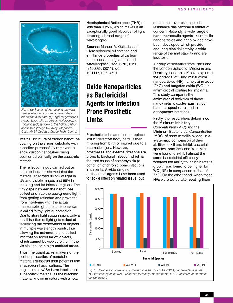
33
r & d h i G h l i G h t s
internal structure of carbon nanotube coating on the silicon substrate with a section purposefully removed to show carbon nanotubes being positioned vertically on the substrate material.
The reflection study carried out on these substrates showed that the material absorbed 99.5% of light in UV and visible ranges and 98% in the long and far infrared regions. The tiny gaps between the nanotubes collect and trap the background light from getting reflected and prevent it from interfering with the actual measurable light; this phenomenon is called ‘stray light suppression’. Due to stray light suppression, only a small fraction of light gets reflected facilitating the observation of objects in multiple wavelength bands, thus allowing the astronomers to collect information about far off objects, which cannot be viewed either in the visible light or in high-contrast areas.
Thus, the quantitative analysis of the optical properties of nanotube materials suggests their potential use in spacecraft applications. The engineers at NASA have labelled this super-black material as the blackest material known in nature with a Total
Fig. 1: (a) Section of the coating showing vertical alignment of carbon nanotubes on the silicon substrate, (b) High-magnification image, taken with an electron microscope, showing a closer view of the hollow carbon nanotubes [Image Courtesy: Stephanie Getty, NASA Goddard Space Flight Centre]
100μm
(a)
(b)
Hemispherical Reflectance (THR) of less than 0.25%, which makes it an exceptionally good absorber of light covering a broad range of wavelengths.
Source: Manuel A. Quijada et al., "Hemispherical reflectance and emittance properties of carbon nanotubes coatings at infrared wavelengths", Proc. SPIE, 8150 (815002), (2011), doi: 10.1117/12.894601
Oxide Nanoparticles as Bactericidal Agents for Infection Prone Prosthetic Limbs
Prosthetic limbs are used to replace lost or defective body parts, either missing from birth or injured due to a traumatic injury. However, prostheses and external fixations are prone to bacterial infection which is the root cause of osteomyelitis (a condition of chronic bone infection) in patients. A wide range of antibacterial agents have been used to tackle infection related issue, but
due to their over-use, bacterial resistance has become a matter of concern. Recently, a wide range of nano-therapeutic agents like metallic nanoparticles and nano-oxides have been developed which provide enduring biocidal activity, a wide range of thermal stability and are less toxic.
A group of scientists from Barts and the London School of Medicine and Dentistry, London, UK have explored the potential of using metal oxide nanoparticles (NP) namely zinc oxide (ZnO) and tungsten oxide (WO3) in antimicrobial coating for implants. This study compares the antimicrobial activities of these nano-metallic oxides against four bacterial species, related to orthopaedic infections.
Firstly, the researchers determined the Minimum Inhibitory Concentration (MIC) and the Minimum Bactericidal Concentration (MBC) of nano-metallic oxides. In a systematic comparison of their abilities to kill and inhibit bacterial species, both ZnO and WO3 NPs were found to exhibit almost the same bactericidal efficiency; whereas the ability to inhibit bacterial growth was found to be higher for WO3 NPs in comparison to that of ZnO. On the other hand, when these NPs were tested after coating them
3000
Conc
entra
tion
(μgm
L-1)
2500
2000
S.aureus E.coli S.epidermidis
Bacterial Species
P.aerugunisa
1500
1000
500
0
ZnO-MIC ZnO-MBC WO3-MIC WO3-MBC
Fig. 1: Comparison of the antimicrobial properties of ZnO and WO3 nano-oxides against four bacterial species (MIC- Minimum inhibitory concentration, MBC- Minimum bactericidal concentration)
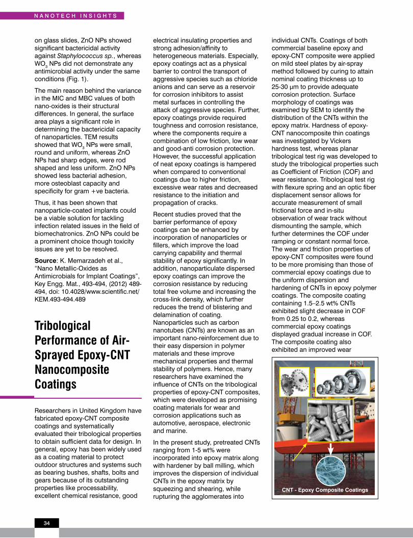
34
Tribological Performance of Air-Sprayed Epoxy-CNT Nanocomposite Coatings
Researchers in United Kingdom have fabricated epoxy-CNT composite coatings and systematically evaluated their tribological properties to obtain sufficient data for design. In general, epoxy has been widely used as a coating material to protect outdoor structures and systems such as bearing bushes, shafts, bolts and gears because of its outstanding properties like processability, excellent chemical resistance, good
n A n o t e c h i n s i G h t s
on glass slides, ZnO NPs showed significant bactericidal activity against Staphylococcus sp., whereas WO3 NPs did not demonstrate any antimicrobial activity under the same conditions (Fig. 1).
The main reason behind the variance in the MIC and MBC values of both nano-oxides is their structural differences. In general, the surface area plays a significant role in determining the bactericidal capacity of nanoparticles. TEM results showed that WO3 NPs were small, round and uniform, whereas ZnO NPs had sharp edges, were rod shaped and less uniform. ZnO NPs showed less bacterial adhesion, more osteoblast capacity and specificity for gram +ve bacteria.
Thus, it has been shown that nanoparticle-coated implants could be a viable solution for tackling infection related issues in the field of biomechatronics. ZnO NPs could be a prominent choice though toxicity issues are yet to be resolved.
Source: K. Memarzadeh et al., “Nano Metallic-Oxides as Antimicrobials for Implant Coatings”, Key Engg. Mat., 493-494, (2012) 489-494, doi: 10.4028/www.scientific.net/KEM.493-494.489
electrical insulating properties and strong adhesion/affinity to heterogeneous materials. Especially, epoxy coatings act as a physical barrier to control the transport of aggressive species such as chloride anions and can serve as a reservoir for corrosion inhibitors to assist metal surfaces in controlling the attack of aggressive species. Further, epoxy coatings provide required toughness and corrosion resistance, where the components require a combination of low friction, low wear and good-anti corrosion protection. However, the successful application of neat epoxy coatings is hampered when compared to conventional coatings due to higher friction, excessive wear rates and decreased resistance to the initiation and propagation of cracks.
Recent studies proved that the barrier performance of epoxy coatings can be enhanced by incorporation of nanoparticles or fillers, which improve the load carrying capability and thermal stability of epoxy significantly. In addition, nanoparticulate dispersed epoxy coatings can improve the corrosion resistance by reducing total free volume and increasing the cross-link density, which further reduces the trend of blistering and delamination of coating. Nanoparticles such as carbon nanotubes (CNTs) are known as an important nano-reinforcement due to their easy dispersion in polymer materials and these improve mechanical properties and thermal stability of polymers. Hence, many researchers have examined the influence of CNTs on the tribological properties of epoxy-CNT composites, which were developed as promising coating materials for wear and corrosion applications such as automotive, aerospace, electronic and marine.
In the present study, pretreated CNTs ranging from 1-5 wt% were incorporated into epoxy matrix along with hardener by ball milling, which improves the dispersion of individual CNTs in the epoxy matrix by squeezing and shearing, while rupturing the agglomerates into
individual CNTs. Coatings of both commercial baseline epoxy and epoxy-CNT composite were applied on mild steel plates by air-spray method followed by curing to attain nominal coating thickness up to 25-30 μm to provide adequate corrosion protection. Surface morphology of coatings was examined by SEM to identify the distribution of the CNTs within the epoxy matrix. Hardness of epoxy-CNT nanocomposite thin coatings was investigated by Vickers hardness test, whereas planar tribological test rig was developed to study the tribological properties such as Coefficient of Friction (COF) and wear resistance. Tribological test rig with flexure spring and an optic fiber displacement sensor allows for accurate measurement of small frictional force and in-situ observation of wear track without dismounting the sample, which further determines the COF under ramping or constant normal force. The wear and friction properties of epoxy-CNT composites were found to be more promising than those of commercial epoxy coatings due to the uniform dispersion and hardening of CNTs in epoxy polymer coatings. The composite coating containing 1.5–2.5 wt% CNTs exhibited slight decrease in COF from 0.25 to 0.2, whereas commercial epoxy coatings displayed gradual increase in COF. The composite coating also exhibited an improved wear
CNT - Epoxy Composite Coatings

35
r & d h i G h l i G h t s
resistance due to higher hardness and reduced friction.
Thus, CNTs were successfully dispersed throughout the matrix up to 3 wt% using ball milling process, which produced relatively uniform dispersion of CNTs in the epoxy matrix. The present epoxy-CNT composite coatings can be used for many practical applications to incorporate anti-corrosion and low friction properties.
Source: H. R. Le et al., “Tribological Characterization of Air-Sprayed Epoxy-CNT Nanocomposite Coatings”, Tribology Letters, 45 (2), (2012) 301-308, doi: 10.1007/s11249-011-9889-0
UV Curable and Transparent Polymer/Clay Nanocomposite Barrier Coatings
Development of polymer/clay nanocomposite films has received considerable attention as building blocks for diffusion barrier films, fire retardants, very strong and ultra-stiff nacre-like layered materials and load-bearing structures due to their unique combination of properties. Layered silicates or clays in particularly have emerged as an important class of nano-fillers due to their ready availability, high aspect ratio, desirable nanostructure and strong interfacial interactions with polymer matrix. In addition, clays can be arranged in an orderly manner as stacked layers within the polymer matrix, which provide tortuous network path that delays the diffusion of gas molecules through the polymer matrix thus providing excellent gas barrier properties. Silicate clays such as Montmorillonite (MMT), Hectorite (HEC) and saponite are the most commonly used clay platelets, which are available with different thicknesses (up to ~1 nm) depending on the number of layers stacked together and have extremely
high aspect ratios (e.g. 50–1000). However, the barrier performance of polymer/clay nanocomposites mainly depends on the individual properties of the nano-filler, the intrinsic barrier of the polymer matrix and the degree of dispersion. It is difficult to achieve complete exfoliation of clay layers in polymer matrix, even after expanding the lateral length or aspect ratio of the clay sheet by various known methods. Recent studies have shown that aspect ratios can be maximized by hydrous suspensions following the organophilization, as it promotes the delamination or
exfoliation spontaneously into thinner platelets with significant aspect ratio by reducing the electrostatic cohesion between the clay stacks. Furthermore, organophilization of hydrous clay suspensions enhances composite properties by improving lipophilicity of clay platelets, whereas polycations are superior modifiers compared to monocations to stabilize clay suspensions in organic solvents.
In the present study, researchers from Germany have established a simple, fast and inexpensive procedure to prepare the diffusion
Flocculation Washing Re-dispersing
Film preparation
UV-Curing
Building block
O2
Organic light-emitting diode (OLED) displays
(i) (ii) (iii) (iv)
(v)
(vi)
(vii)(vii)
(vii)
Flexible packaging
Thin film transistor liquid crystal display
Schematic representation of process steps of UV-curable barrier coatings: (i) aqueous dispersions of clay particles are flocculated via the addition of ccPU-dispersion, (ii) loose aggregates of obtained clay hybrids are washed with water, (iii) re-dispersed in THF, (iv) preparation of homogeneous composite films of clay hybrid-dispersions by doctor-blading method, (v) final curing by UV-radiation cross-links the ccPU on both sides of the clay lamella of O-HEC hybrid-platelet, which improves oxygen-barrier and insolubility of the composite coating and (vii) illustrates the corresponding applications of barrier composite films.
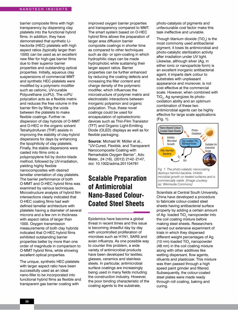
36
n A n o t e c h i n s i G h t s
Scalable Preparation of Antimicrobial Nano-Based Colour-Coated Steel Sheets
Epidemics have become a global threat in recent times and this issue is becoming dreadful day by day with uncontrolled proliferation of microbes such as H1N1, SARS and avian influenza. As one possible way to counter this problem, a wide variety of antimicrobial products have been developed for textiles, glasses, ceramics and stainless steels. In particular, antimicrobial surface coatings are increasingly being used in many fields including the construction industry. However, the poor binding characteristic of the coating agents to the substrate,
barrier composite films with high transparency by dispersing clay platelets into the functional hybrid films. In addition, they have demonstrated that synthetic Li-hectorite (HEC) platelets with high aspect ratios (typically larger than 1000) can be used as an excellent new filler for high-gas barrier films due to their superior barrier properties and outstanding optical properties. Initially, aqueous clay suspensions of commercial MMT and synthetic HEC-platelets were modified by a polymeric modifier such as cationic, UV-curable Polyurethane (ccPU). The ccPU polycation acts as a flexible matrix and reduces the free volume in the barrier film by filling the voids between the platelets to make flexible coatings. Further re-dispersion of clay hybrids of O-MMT and O-HEC in the organic solvent Tetrahydrofuran (THF) assists in improving the stability of clay-hybrid dispersions for days by enhancing the lipophilicity of clay platelets. Finally, the stable dispersions were casted into films onto a polypropylene foil by doctor-blade method, followed by UV-irradiation, yielding highly flexible nanocomposites with desired lamellar orientation of clay platelets. The barrier performance of both O-MMT and O-HEC hybrid films was examined by various techniques. Microstructure analysis of hybrid film intersections clearly indicated that O-HEC coating films had well-defined lamellar architecture with platelets having a diameter of several microns and a few nm in thickness with aspect ratios of larger than 1000. Oxygen transmission measurements of both clay hybrids indicated that O-HEC hybrid films exhibited outstanding barrier properties better by more than one order of magnitude in comparison to O-MMT hybrid films, while showing excellent optical properties.
The unique, synthetic HEC-platelets with larger aspect ratio have been successfully used as an ideal nano-filler to be incorporated into functional hybrid films as flexible and transparent gas barrier coating with
improved oxygen barrier properties and transparency compared to MMT. The smart system based on O-HEC hybrid films allows the preparation of larger area diffusion barrier composite coatings in shorter time as compared to other techniques such as dip- or spin-coating in which hydrophilic clays can be made hydrophobic while sustaining their larger aspect ratios. Barrier properties can be further enhanced by reducing the coating defects and increasing the filler content and charge density of the polymeric modifier, which influences the microstructure of polymer matrix and electrostatic interactions between inorganic polyanion and organic polycation. Thus, these novel coatings could be used for encapsulation of optoelectronic devices such as Thin-Film Transistor (TFT) and Organic Light-Emitting Diode (OLED) displays as well as for flexible packaging.
Source: Michael W. Möller et al., “UV-Cured, Flexible, and Transparent Nanocomposite Coating with Remarkable Oxygen Barrier”, Adv. Mater., 24 (16), (2012) 2142–2147, doi: 10.1002/adma.201104781
photo-catalysis of pigments and unfavourable cost factor make this task ineffective and unviable.
Though titanium dioxide (TiO2) is the most commonly used antibacterial pigment, it loses its antimicrobial and photo-catalytic sterilization activity after irradiation under UV light. Likewise, although silver (Ag, in either ionic or nanoparticle form) is an excellent inorganic antibacterial agent, it imparts dark colour to substrates with unpleasant appearance and moreover, is not cost effective at the commercial scale. However, when combined with TiO2, Ag synergizes its photo-oxidation ability and an optimum combination of these two antimicrobial agents can be highly effective for large scale applications (Fig. 1).
Scientists at Central South University, China have developed a procedure to fabricate colour-coated steel sheets having antibacterial surface property by adding a certain amount of Ag- loaded TiO2 nanopowder into the coil coating mixture before making steel sheets. Researchers carried out extensive experiment of trials in which they dispersed different weight percentages of Ag (10 nm)-loaded TiO2 nanopowder (48 nm) in the coil coating mixture along with other additives like wetting dispersant, flow agents, diluents and plasticizer. This mixture was then passed through a high speed paint grinder and filtered. Subsequently, the colour-coated steel plates were made ready through roll coating, baking and curing.
Nano-Based Colour-Coated Steel Sheets
Ag-Loaded TiO2Nanoparticles
Photo-Oxidation
Inhibits Microbial Growth
Kills Harmful Bacteria
Suitable for Industrial Scale
O2-OH
Fig. 1: The photo-catalytic nanocoating destroys harmful bacteria, inhibits microbial growth on treated surfaces and is commercially viable. [Image courtesy (a): Wikimedia Commons]
(a)

37
r & d h i G h l i G h t s
All ingredients became a part of the final product that showed an increased antibacterial efficiency up to 99.99% and photo-catalytic property up to 88%. Based on the present study, the optimal Ag-loaded TiO2 content was found to be 2 wt% to achieve the maximum antibacterial efficiency (Fig. 2). Also, at higher rotational speed, paint grinder produced finer coil coating and more glossy sheets except a few reagglomerated nanoparticles, which were meeting the target properties. However, stability of this coating decreased over time because of the flocculation of nanoparticles, but no Ag+ leaching was reported, which proved its durability. Finally, a pilot-scale run was carried out to assess the commercial feasibility of this technology. The pilot-scale study has clearly indicated that the technology is commercially viable and can result into products meeting with the required standard.
Superhydrophobic DLC Coating for Advanced Protective Applications
In recent times, functional surfaces with bio-mimicking micro-textures have gained much attention due to their potential applications such as hydrophobic, anti-adhesive, antifogging and self-cleaning agents. Many attempts have been made to attain water-repelling surfaces, similar to natural lotus-leaf, decorated with hydrophobic bumpy and waxy structures with self-cleaning function and low hysteresis. However, these surfaces are soft, which limits their use in specific areas such as cutting tools and magnetic hard disks due to the lack of high hardness, low surface energy and high wear-resistance. Recently, Diamond-like Carbon (DLC) films have been considered for use as functional surfaces for various potential applications due to their outstanding properties such as high hardness, wear-resistance, low Coefficient of Friction (COF), optical transparency, chemical inertness and electrical insulation. However, only
few studies have been reported to fabricate superhydrophobic and flexible DLC films, as the intrinsic hydrophilic properties of DLC limit their applications.
Development of DLC films with bio-mimicking micro-textures as superhydrophobic films as well as engineered materials, which lower the surface energy while retaining their high hardness and a high wear and frictional resistance have been considered as a new challenge to expand the applications of DLC films. In the present study, researchers from China and UK have established a novel approach to fabricate hard, flexible and superhydrophobic DLC films with bio-mimicking micro-textures using natural lotus leaf as a template by combining the processes like nanocasting, electroplating method and physical vapor deposition (Fig. 1). The prepared DLC (Lotus) films were further modified with Perfluoropolyether (PFPE) lubricant to obtain superhydrophobic surface and to maintain relatively low COF. Micro-structural characterization and mechanical property evaluation of the obtained DLC (Lotus) films were done by well-known techniques. Raman spectroscopy clearly indicated the presence of diamond-like carbon
PDMS
Biological sample
Gold target
(a)
(b)
(c) (d)
(e)
(f)
Negative impression of the bio-mimicking textures
Positive impression of the bio-mimicking textures
Gold sputtered PDMS
Nickel anode
Solution
PDMS
Nickel film
AuTi
DLC filmBio-mimicking textures
Au
Nickel film
Graphite Target
Plasma
Substrates bracket (Patterned metal film)
Plasma
Fig. 1: The schematic view of creating DLC film with bio-mimicking textures: (a) A PDMS film is used to replicate the surface micro-textures of the biological sample (lotus), (b) a thin layer of gold is sputtered on the textured PDMS film to provide a conductive surface, (c) Ni-metallic layer is electro-deposited on the top of the PDMS film, (d) the PDMS film is peeled off to obtain a Ni-metallic layer with positive impression of the bio-mimicking textures, (e) a thin hard Ti-incorporated DLC film is deposited on the top of the Ni-metallic layer, (f) DLC film with bio-mimicking textures.
800000
600000
400000
200000
700000
500000
300000
01 2 3 4
100000
The dose of Ag/TiO2/wt%
Colo
ny F
orm
ing
Units Bacterial count #3
Bacterial count #2Bacterial count #1
Fig. 2: Comparison of antibacterial properties of different weight percentages of Ag-loaded TiO2 nanopowder
Thus, this innovative approach is capable of producing antimicrobial colour-coated steel sheets, which are cost-effective at industrial scale, durable and have excellent photo-catalytic surface properties. Moreover, nanoparticles used in the coating make it more efficient than non-nano-based coatings in terms of antibacterial properties which could be beneficial for various sectors including the construction industry.
Source: Guoliang Li et al., “Preparation of Antibacterial Color-Coated Steel Sheets”, Int. Jour. Phen., (2012), Article ID: 436963, doi: 10.1155/2012/436963
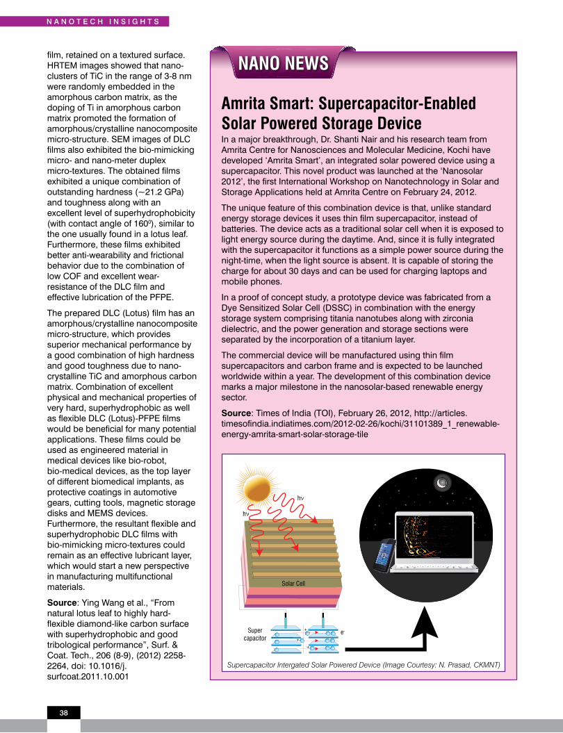
38
n A n o t e c h i n s i G h t s
film, retained on a textured surface. HRTEM images showed that nano-clusters of TiC in the range of 3-8 nm were randomly embedded in the amorphous carbon matrix, as the doping of Ti in amorphous carbon matrix promoted the formation of amorphous/crystalline nanocomposite micro-structure. SEM images of DLC films also exhibited the bio-mimicking micro- and nano-meter duplex micro-textures. The obtained films exhibited a unique combination of outstanding hardness (~21.2 GPa) and toughness along with an excellent level of superhydrophobicity (with contact angle of 1600), similar to the one usually found in a lotus leaf. Furthermore, these films exhibited better anti-wearability and frictional behavior due to the combination of low COF and excellent wear-resistance of the DLC film and effective lubrication of the PFPE.
The prepared DLC (Lotus) film has an amorphous/crystalline nanocomposite micro-structure, which provides superior mechanical performance by a good combination of high hardness and good toughness due to nano-crystalline TiC and amorphous carbon matrix. Combination of excellent physical and mechanical properties of very hard, superhydrophobic as well as flexible DLC (Lotus)-PFPE films would be beneficial for many potential applications. These films could be used as engineered material in medical devices like bio-robot, bio-medical devices, as the top layer of different biomedical implants, as protective coatings in automotive gears, cutting tools, magnetic storage disks and MEMS devices. Furthermore, the resultant flexible and superhydrophobic DLC films with bio-mimicking micro-textures could remain as an effective lubricant layer, which would start a new perspective in manufacturing multifunctional materials.
Source: Ying Wang et al., “From natural lotus leaf to highly hard-flexible diamond-like carbon surface with superhydrophobic and good tribological performance”, Surf. & Coat. Tech., 206 (8-9), (2012) 2258-2264, doi: 10.1016/j.surfcoat.2011.10.001
Amrita Smart: Supercapacitor-Enabled Solar Powered Storage DeviceIn a major breakthrough, Dr. Shanti Nair and his research team from Amrita Centre for Nanosciences and Molecular Medicine, Kochi have developed ‘Amrita Smart’, an integrated solar powered device using a supercapacitor. This novel product was launched at the ‘Nanosolar 2012’, the first International Workshop on Nanotechnology in Solar and Storage Applications held at Amrita Centre on February 24, 2012.
The unique feature of this combination device is that, unlike standard energy storage devices it uses thin film supercapacitor, instead of batteries. The device acts as a traditional solar cell when it is exposed to light energy source during the daytime. And, since it is fully integrated with the supercapacitor it functions as a simple power source during the night-time, when the light source is absent. It is capable of storing the charge for about 30 days and can be used for charging laptops and mobile phones.
In a proof of concept study, a prototype device was fabricated from a Dye Sensitized Solar Cell (DSSC) in combination with the energy storage system comprising titania nanotubes along with zirconia dielectric, and the power generation and storage sections were separated by the incorporation of a titanium layer.
The commercial device will be manufactured using thin film supercapacitors and carbon frame and is expected to be launched worldwide within a year. The development of this combination device marks a major milestone in the nanosolar-based renewable energy sector.
Source: Times of India (TOI), February 26, 2012, http://articles.timesofindia.indiatimes.com/2012-02-26/kochi/31101389_1_renewable-energy-amrita-smart-solar-storage-tile
hν
hν
Solar Cell
Supercapacitor Intergated Solar Powered Device (Image Courtesy: N. Prasad, CKMNT)
e-Super capacitor
NANO NEWS

39
Indian Scenario
Emerging Trends of Nanoscience and Nanotechnology in IndiaIntroductionNanotechnology is one of the emerging fields of Science and Technology (S&T) research in India and has generated enormous interest in the global research community as well. Undoubtedly, nano technology has tremendous application potential in several areas such as electronics, optics, biotechnology, healthcare, medicine, energy, aerospace, defence, etc., where it has offered many opportunities to improve conventional technologies.
Though in India, nanotechnology emerged in the late 1990s, the actual thrust was imparted in 2001, when the Government of India announced its policy to promote and support nanotechnology related activities with the establishment of “Nano Science and Technology Initiative (NSTI)” and “Nano Mission” (under the Department of Science & Technology (DST) with an initial plan drawn and carried out during the Xth Five Year Plan (2002-07) and XIth Five Year Plan (2007–12), respectively with the budget allocation of `1000 crores.
Statistics (Source: Google TrendsTM) show that nanotechnology was the most searched topics in India than any other country during the period of January, 2004 and December, 2011.
In India, the enormous public interest in nanoscience and nanotechnology has apparently been spurred by the strong and concrete support from the Government of India through
various funding schemes and the collective efforts of DST and the Centre for Knowledge Management of Nanoscience and Nanotechnology (CKMNT), Hyderabad, India.
The nanotechnology-related publications have grown considerably during the last decade all over the world. An elaborate analysis is required to ascertain the contribution of Indian researchers to this futuristic field. Bibliometric analysis is a solution for getting integrated perspective of the state of Indian nanotechnology research from the voluminous literature. This article analyses the nanoscience and nanotechnology research literature of India and identifies India’s core competencies in this field.
Data CollectionLiterature analysis is an important source of scientific and technological information that highlights technological trends, key academic institutions and R&D organizations along with their competitive intelligences.
A detailed literature analysis has been carried out to understand the Indian scenario of nanotechnology research using the journals, published worldwide during the period of 2001-2011 (sizable number of records were available from 2001 only) with the help of Web of Science® (WoS), the world’s most popular Abstracting & Indexing (A&I) database.
Since nanotechnology is a multidisciplinary field, nanotechnology related papers are published in a variety of journals. The following search string has been implemented to extract the journals published worldwide on nanoscience and nanotechnology within a specific period:
Approach 1:Search string: (((TS = (nano* not (nano2 or nano3 or nanoinden* or nanogram* or nanosecond* or nanohenri* or nanobod* or nanoinstruction*)) and CU = (India))))
Databases=SCI-EXPANDED, CPCI-S, CPCI-SSH
Time span= January 01, 2001 to December 31, 2011
Results: 21867 records1
The search retrieved a data set of 21867 records, but in-depth analysis has been done for only 16900 records, as these records contain only those authors (First), who carried out their research work in India. All these records were analyzed further to meet the objective of this study such as most prolific authors and institutions, journals that published numerous nanotechnology papers and also the most frequently cited papers. It should be noted that this data set was created on 31st December 2011. If this analysis is done today, there may be slight variations in terms of citations and h-index as publications get citations regularly and WoS is updated daily.
Publications Analysis & Discussions
Year Wise GrowthIndian publications on nanoscience and nanotechnology have increased with an average annual growth rate of 28% in the past ten years. Table 1 highlights the trend of nanotechnology-related scientific publications in India in the last ten years (2001-2011), which indicates that though the number of publications has increased during these years, but yearly growth of
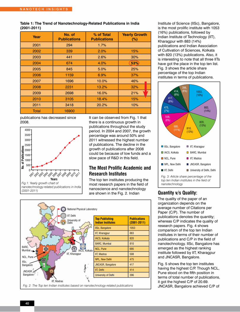
40
publications has decreased since 2008.
It can be observed from Fig. 1 that there is a continuous growth in publications throughout the study period. In 2004 and 2007, the growth percentage was around 50% and 2011 witnessed the highest number of publications. The decline in the growth of publications after 2008 could be because of low funds and a slow pace of R&D in this field.
The Most Prolific Academic and Research InstitutesThe top ten institutes producing the most research papers in the field of nanoscience and nanotechnology are shown in the Fig. 2. Indian
Institute of Science (IISc), Bangalore, is the most prolific institute with 1053 (16%) publications, followed by Indian Institute of Technology (IIT), Kharagpur with 883 (14%) publications and Indian Association of Cultivation of Sciences, Kolkata with 820 (13%) publications. Also, it is interesting to note that all three IITs have got the place in the top ten list. Fig. 3 shows the article share percentage of the top Indian institutes in terms of publications.
Year No. of
Publications% of Total
PublicationsYearly Growth
(%)
2001 294 1.7%
2002 339 2.0% 15%
2003 441 2.6% 30%
2004 674 4.0% 53%
2005 845 5.0% 25%
2006 1159 6.9% 37%
2007 1696 10.0% 46%
2008 2231 13.2% 32%
2009 2698 16.0% 21%
2010 3105 18.4% 15%
2011 3418 20.2% 10%
Total 16900
Table 1: The Trend of Nanotechnology-Related Publications in India (2001-2011)
4000
3500
3000
2500
2000
2001
2002
2003
2004
2005
2006
Years
No. o
f Pub
licat
ions
2007
2008
2009
2010
2011
1500
1000
500
0
Fig.1: Yearly growth chart of nanotechnology-related publications in India (2001-2011)
Top Publishing Indian Institutes
Publications (2001-2011)
IISc, Bangalore 1053
IIT, Kharagpur 883
IACS, Kolkata 820
BARC, Mumbai 810
NCL, Pune 695
IIT, Madras 508
NPL, New Delhi 475
JNCASR, Bangalore 417
IIT, Delhi 414
University of Delhi 396
New Delhi
National Physical Laboratory
IIT Delhi
University of Delhi
BARC, Mumbai
Government of India
IISc, Bangalore
JNCASR, Bangalore
NCL, Pune
IIT, Madras
IIT, KharagpurIACS, Kolkata
Fig. 2: The Top ten Indian institutes based on nanotechnology-related publications
396, (6%) 1053,
(16%)
883, (14%)
820, (13%)
810, (13%)
695, (11%)
508, (8%)
475, (7%)
417, (6%)
414, (6%)
IISc, Bangalore
IACS, Kolkata
NCL, Pune
NPL, New Delhi
IIT, Delhi
IIT, Kharagpur
BARC, Mumbai
IIT, Madras
JNCASR, Bangalore
University of Delhi, Delhi
Fig. 3: Article share percentage of the top ten Indian institutes in the field of nanotechnology
Quantity v/s Quality:The quality of the paper of an organization depends on the average number of Citations per Paper (C/P). The number of publications denotes the quantity; whereas C/P indicates the quality of research papers. Fig. 4 shows comparison of the top ten Indian institutes in terms of their number of publications and C/P in the field of nanotechnology. IISc, Bangalore has emerged as the highest ranking institute followed by IIT, Kharagpur and JNCASR, Bangalore.
Fig. 5 shows the top ten institutes having the highest C/P. Though NCL, Pune stood on the fifth position in terms of total number of publications, it got the highest C/P of 20.69. JNCASR, Bangalore achieved C/P of
n A n o t e c h i n s i G h t s

41
i n d i A n s c e n A r i o
18.37, even though it was ranked at the eighth position in terms of total number of publications. Further, IISc, Bangalore published the highest number of papers but it could achieve C/P of 13.51 and hence secured third position in the ranking.
In general, researchers/institutes are rated on the basis of their number of publications; however, this methodology emphasizes more on quantity than quality. Jorge E. Hirsh, a physicist from University of California introduced a new bibliometric measure, h-index (a ranking tool); to characterize scientific output of researchers based on their publication records. The h-index measures impact factor and productivity of publications of researchers.
The same concept has been applied
in this analysis to rank Indian institutions in order to assess the quality of their publications (Fig. 6). It is interesting to note that though NCL, Pune is at the seventh position in terms of total number of publications; it has secured the highest h-index of 59. It is followed by IISc, Bangalore and JNCASR with h-indices 52 and 44, respectively.
The Top Twenty Impact Factor (IF) Journals (Worldwide)The Impact Factor (IF) of a journal reflects the average number of citations received by published articles. IFs for the journals are released by Thomson Reuters every year as ‘Journal Citation Reports (JCR)’. Usually, researchers prefer to publish their research findings in journals with high IFs, for getting better value and visibility of their publications.
In this analysis, we have tried to find out nanotechnology-based publications of Indian researchers in the top twenty journals (worldwide) in terms of IF. The following search string has been used to extract this information:
8.24
8.39
8.64
9.31
9.39
10.49
12.96
13.51
0 10 20 30
18.37
20.69
IISc, Bangalore
IACS, Kolkata
NCL, Pune
NPL, New Delhi
IICT, Hyderabad
IIT, Kharagpur
BARC, Mumbai
IIT, Madras
JNCASR, Bangalore
Avg.citations/paper
Top
10 In
stitu
tes
University of Delhi
Fig. 5: The top ten Indian institutes based on C/P in nanotechnology domain
1100
1000
900
800
700
600
500
hh
hh
h
hhh
h
h
400
3003 10 174 11 185 12 196 13 207 14 218 15 22
60
40
50
30
20
109 16
No. o
f Pub
licat
ions
Avg. citations/paper (c/p)
h-In
dex
IISc, Bangalore
IACS, Kolkata
NCL, Pune
NPL, New Delhi
IIT, Delhi
IIT, Kharagpur
BARC, Mumbai
IIT, Madras
JNCASR, Bangalore
University of Delhi, Delhi
'h' indicates h-Index 'c/p' Indicates Avg. citations/paper
Fig. 4: Comparison of the average number of citations per paper (C/P) and h-index of the top ten Indian institutes in the field of nanotechnology
c/p c/p
c/pc/p
c/pc/p
c/p
c/p
c/pc/p
**
IISc,
Banga
lore
IACS, Kolk
ata
IICT,
Hydera
bad
IIT, Kha
ragpu
r
BARC, Mum
bai
IIT, M
adras
JNCASR, B
anga
lore
Univers
ity of
Delhi
NPL, New
Delhi
60
50
40
30
20
10
0
h-In
dex
Fig. 6: The Top ten Indian institutes on the basis of h-index
Top 10 Institutes
NCL, Pun
e

42
n A n o t e c h i n s i G h t s
# Journal Publisher IF (2010)
1Nature Nanotechnology
Nature Group 30.306
2 Nano Letters American Chemical Society (ACS) 12.186
3 Nano Today Elsevier Science 11.750
4 Advanced Materials Wiley-VCH 10.857
5 ACS Nano American Chemical Society (ACS) 9.855
6Advanced Functional Materials
Wiley-VCH 8.486
7 Small Wiley-VCH 7.333
8 Lab on a Chip Royal Society of Chemistry (RSC) 6.260
9 Nanomedicine Future Medicine Ltd 6.202
10Biosensors & Bioelectronics
Elsevier Science 5.361
11 Nano Research Springer 5.071
12International Journal of Nanomedicine
Dove Medical Press Ltd 4.976
13
Nanomedicine-Nanotechnology, Biology and Medicine
Elsevier Science 4.882
14Journal of Physical Chemistry – C
American Chemical Society (ACS) 4.520
15 Biomicrofluidics American Institute of Physics (AIP) 3.896
16 Nanotoxicology Informa Healthcare 3.880
17 Nanotechnology Institute of Physics (IOP) 3.644
18 Plasmonics Springer 3.526
19Microfluidics and Nanofluidics
Springer 3.504
20Biomedical Microdevices
Springer 3.386
Table 2: The Top Twenty Worldwide Journals in Terms of Impact Factor2 (IF)
Approach 2:TS=((nano* OR quantum wire* OR quantum dot* OR graphene) NOT (nano2 OR nano3)) AND CU=(india) AND PY=(2001-2010) AND SO=(NATURE NANOTECHNOLOGY OR NANO LETTERS OR NANO TODAY OR ADVANCED MATERIALS OR ACS NANO OR ADVANCED FUNCTIONAL MATERIALS OR SMALL OR LAB ON A CHIP OR NANOMEDICINE OR BIOSENSORS BIOELECTRONICS OR NANO RESEARCH OR INTERNATIONAL JOURNAL OF NANOMEDICINE OR NANOMEDICINE NANOTECHNOLOGY BIOLOGY AND MEDICINE OR JOURNAL OF PHYSICAL CHEMISTRY C OR
IISc,
Banga
lore
IACS, Kolk
ata
NCL, Pun
e
IIT, Kha
ragpu
r
BARC, Mum
bai
IIT, M
adras
JNCASR, B
anga
lore
Univers
ity of
Pune
NPL, New
Delhi
IIT-D
elhi, D
elhi
120
100
80
60
40
20
0
No. o
f Pub
licat
ions
Fig. 7: Nanotechnology-related publications of the top ten Indian institutes in the top twenty IF journals (worldwide)
Top 10 Institutes
BIOMICROFLUIDICS OR NANOTOXICOLOGY OR NANOTECHNOLOGY OR PLASMONICS OR MICROFLUIDICS AND NANOFLUIDICS OR BIOMEDICAL MICRODEVICES)
Databases=SCI-EXPANDED, CPCI-S, CPCI-SSH
Time span= January 01, 2001 to December 31, 2011
Results: 778 records1
The above search generated a data set of 778 records. This data set has been further examined to understand the performance of various Indian academic and R&D institutes (Table 2).
Fig. 7 shows the publication trend of the ten most prolific Indian institutions. It is apparent from the graph that IACS, Kolkata has published 106, the most of publications; followed by IISc, Bangalore and NCL, Pune with 82 and 48 publications, respectively. These figures reveal the growing interest of Indian researchers to publish their research findings in high IF journals for better attention and visibility of their publications.
It is evident from Fig. 8 that JNCASR, Bangalore achieved the highest C/P of 23.23 followed by NCL, Pune (22.15) and BHU, Varanasi (20.69). Additionally, IISc, Bangalore and JNCASR, Bangalore secured the
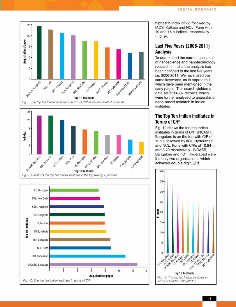
43
i n d i A n s c e n A r i o
30
35
40
25
20
15
10
5
0
h-In
dex
Fig. 11: The top ten Indian institutes in terms of h-index (2006-2011)
Top 10 Institutes
highest h-index of 22, followed by IACS, Kolkata and NCL, Pune with 19 and 16 h-indices, respectively (Fig. 9).
Last Five Years (2006-2011) AnalysisTo understand the current scenario of nanoscience and nanotechnology research in India, the analysis has been confined to the last five years i.e. 2006-2011. We have used the same keywords, as in approach 1, which have been mentioned in the early pages. This search yielded a data set of 14307 records, which were further analyzed to understand nano-based research in Indian institutes.
The Top Ten Indian Institutes in Terms of C/PFig. 10 shows the top ten Indian institutes in terms of C/P. JNCASR, Bangalore is on the top with C/P of 12.57, followed by IICT, Hyderabad and NCL, Pune with C/Ps of 10.84 and 8.79 respectively. JNCASR, Bangalore and IICT, Hyderabad were the only two organizations, which achieved double digit C/Ps.
0 2 4 6 8 10 12 14
IISc, Bangalore
IACS, Kolkata
NCL, Pune
NPL, New Delhi
IICT, Hyderabad
IIT, Kharagpur
RRI, Bangalore
IIT, Madras
JNCASR, Bangalore
Avg.citations/paper
Top
10 In
stitu
tes
CERI, Karaikudi
Fig. 10: The top ten Indian institutes in terms of C/P
IACS,
Bang
alore
IICT,
Hydera
bad
IIT, Kh
aragp
urBA
RC, Mum
bai
JNCAS
R, Ban
galor
e
Univers
ity of
Delh
i
NPL, N
ew D
elhi
25
20
15
10
5
0
Avg.
cita
tions
/pap
er
Fig. 8: The top ten Indian institutes in terms of C/P in the top twenty IF journalsTop 10 Institutes
NCL, Pu
neBH
U, Ban
aras
Univers
ity of
Pune
NCL, Pun
e
IIT, M
adras
IACS,
Kolka
ta
IICT,
Hydera
bad
IIT, Kh
aragp
urBA
RC, Mum
bai
JNCAS
R, Ban
galor
e
BHU, B
anara
s
NPL, N
ew D
elhi
25
20
15
10
5
0
h-In
dex
Fig. 9: h-index of the top ten Indian institutes in the top twenty IF journalsTop 10 Institutes
IISc,
Bang
alore
IISc,
Banga
lore
IACS, Kolk
ata
IIT, Kha
ragpu
r
BARC, Mum
bai
JNCASR, B
anga
lore
NPL, New
Delhi
NCL, Pun
e
IIT, M
adras
IICT,
Hydera
bad
Univ. o
f Delh
i, Delh
i

44
n A n o t e c h i n s i G h t s
The Top Ten Indian Institutes in Terms of h-indexIn this analysis, IISc, Bangalore has achieved the highest h-index of 37, followed by JNCASR, Bangalore and IACS, Kolkata with equal h-indices of 32 (Fig. 11). However, the h-index ranks old papers higher than the recently published ones; therefore, the h-index for the period of 2001-2010 had a higher value than the last five years.
The Top Ten Most-Cited Papers of Indian OriginFollowing are the top ten most-cited Indian papers including seven review articles based on ‘Average Citations per Year (ACY)’. It is interesting to note that majority of the articles have been a product of a collaboration of two or more institutes, which is going in the favour of papers for getting high degree of visibility.
1. CNR Rao, AK Sood, KS Subrahmanyam, A Govindaraj, “Graphene: The New Two-Dimensional Nanomaterial”, Angewandte Chemie-International Edition, 48 (42), (2009) 7752-7777 ACY: 120.33 (Review)
2. Mahendra Rai, Alka Yadav, Aniket Gad, “Silver nanoparticles as a new generation of antimicrobials”, Biotechnology Advances, 27 (1), (2009) 76-83 ACY: 70.33 (Review)
3. SK Ghosh, T Pal, “Interparticle coupling effect on the surface plasmon resonance of gold nanoparticles: From theory to applications”, Chemical Reviews, 107 (11), (2007) 4797-4862 ACY: 58.6 (Review)
4. A Ajayaghosh, VK Praveen, “pi-organogels of self-assembled p-phenylenevinylenes: Soft materials with distinct size, shape, and functions” Accounts of Chemical Research, 40 (8), (2007) 644-656 ACY: 56 (Review)
5. A Sundaresan, R Bhargavi, N Rangarajan, U Siddesh, CNR Rao, “Ferromagnetism as a
universal feature of nanoparticles of the otherwise nonmagnetic oxides”, Physical Review B, 74 (16), (2006) ACY: 53.66
6. CNR Rao, FL Deepak, G Gundiah, A Govindaraj, “Inorganic nanowires”, Progress in Solid State Chemistry, 31 (1-2), (2003) 5-147 ACY: 52.11 (Review)
7. SS Shankar, A Rai, B Ankamwar, A Singh, A Ahmad, M Sastry, “Biological synthesis of triangular gold nanoprisms”, Nature Materials, 3 (7), (2004) 482-488 ACY: 50.37
8. SA Agnihotri, NN Mallikarjuna, TM Aminabhavi, “Recent advances on chitosan-based micro- and nanoparticles in drug delivery”, Journal of Controlled Release, 100 (1), (2004) 5-28 ACY: 48.87 (Review)
9. P Sharma, R Varma, RC Sarasij, K Gousset, G Krishnamoorthy, M Rao, S Mayor, “Nanoscale organization of multiple GPI-anchored proteins in living cell membranes”, Cell, 116 (4), (2004) ACY: 46.62
10. A Ajayaghosh, VK Praveen, C Vijayakumar, “Organogels as scaffolds for excitation energy transfer and light harvesting”, Chemical Society Reviews, 37 (1), (2008) 109-122, ACY: 42.50 (Review)
The Top Ten Most-Cited Papers (Research Articles Only)Because of the nature of the content of review papers, they naturally get more citations in comparison to original research papers. Hence it is justifiable for us to bring out the highly cited original research papers by Indian researchers in nanoscience and nanotechnology area. Following are the top ten most-cited research papers of Indian authors:
1. A Sundaresan, R Bhargavi, N Rangarajan, U Siddesh, CNR Rao, “Ferromagnetism as a universal feature of nanoparticles
of the otherwise nonmagnetic oxides”, Physical Review B, 74 (16), (2006) ACY: 53.66
2. SS Shankar, A Rai, B Ankamwar, A Singh, A Ahmad, M Sastry, “Biological synthesis of triangular gold nanoprisms”, Nature Materials, 3 (7), (2004) 482-488 ACY: 50.37
3. P Sharma, R Varma, RC Sarasij, K Gousset, G Krishnamoorthy, M Rao, S Mayor, “Nanoscale organization of multiple GPI-anchored proteins in living cell membranes”, Cell, 116 (4), (2004) ACY: 46.62
4. BM Choudary, S Madhi, NS Chowdari, ML Kantam, B Sreedhar, “Layered double hydroxide supported nanopalladium catalyst for Heck-, Suzuki-, Sonogashira-, and Stille-type coupling reactions of chloroarenes”, Journal of the American Chemical Society, 124 (47), (2002) 14127-14136 ACY: 40.44
5. R Shukla, V Bansal, M Chaudhary, A Basu, RR Bhonde, M Sastry, “Biocompatibility of gold nanoparticles and their endocytotic fate inside the cellular compartment: A microscopic overview”, Langmuir, 21 (23), (2005) 10644-10654 ACY: 38.85
6. M Sathish, B Viswanathan, RP Viswanath and CS Gopinath, “Synthesis, characterization, electronic structure, and photocatalytic activity of nitrogen-doped TiO2 nanocatalyst”, Chemistry of Materials, 17 (25), (2005) 6349-6353 ACY: 31.85
7. G Galgali, C Ramesh, A Lele, “A rheological study on the kinetics of hybrid formation in polypropylene nanocomposites”, Macromolecules, 34 (4), (2001) 852-858 ACY: 29.81

45
Nano-Silver: A Novel Approach to Treat FilariasisFilariasis is one of the major public health threats, especially prevailing in tropical and subtropical regions of the world. It is caused by nematodes (roundworms) in the superfamily filarioidea. The most dreaded type of filariasis is lymphatic filariasis (Elephantiasis) characterized by edema with swelling of the skin and underlying tissues. The disease is caused by microscopic worms, microfilariae that lodge itself into the lymphatic system including the lymph nodes which ultimately leads to elephantiasis. The mosquito bites cause the infection to spread from person to person. According to the WHO estimates, over 120 million people are currently infected worldwide, out of which about 40 million people infected with the disease live in India.A recent study jointly conducted by the researchers at Banaras Hindu University, Varanasi and Mahatma Gandhi Institute of Medical Sciences, Sevagram suggested that silver nanoparticles (10-15 nm particle size) act as potent microfilaricidal agent against Brugia malayi in vitro. Silver nanoparticles play a major role as an adjuvant, when taken in combination with a conventional anti-filarial drug, Diethyl-carbamazine Citrate (DEC). Silver nanoparticles are quite well known for their antibacterial activities by inducing apoptosis in eukaryotic cells and the present study has clearly established the validity of the premise of apoptotic death of filaricidal parasite rationale. The present study opens new avenues to design the potent drugs to combat the deadly elephantiasis.
Source: S. K. Singh et al., “Novel microfilaricidal activity of nanosilver”, Int. Jour. Nanomed., 7, (2012) 1023-1030, doi: 10.2147/IJN.S28758
NANO NEWS
(a) The life cycle of Wuchereria bancrofti (one of the parasites that cause lymphatic filariasis) (b) A person suffering from elephantiasis
Filariasis
Mosquito Stages Human Stages
(Wuchereria bancrofti)
Mosquito takes a blood meal
Migrate to head and mosquito's proboscis
Mosquito takes a blood meal (ingests
microfilariae)
Microfilariae shed sheaths, pentrate mosquito's midgut, and migrate to theracic muscles
(L3 larvae enter skin)
L3 larvae
Adults produce sheathed microfilariae that migrate into lymph and blood channels
Adults in lymphatics
= Infective Stage
= Diagnostic Stage
L1 larvae
1
8
4
7
3
2
6
5
d
d i
i
(b)
(a)
Contributed by Vivek Patel, CKMNT and R. Vijaya Chandar, ARCI
8. PK Sudeep, STS Joseph, KG Thomas, “Selective detection of cysteine and glutathione using gold nanorods”, Journal of the American Chemical Society, 127 (18), (2005) 6516-6517 ACY: 29.28
9. S Ghosh, AK Sood, N Kumar, “Carbon nanotube flow sensors”, Science, 299 (5609), (2003) 1042-1044, ACY: 28.55
10. SP Chandran, M Chaudhary, R Pasricha, A Ahmad, M Sastry, “Synthesis of gold nanotriangles and silver nanoparticles using Aloe vera plant extract”, Biotechnology Progress, 22 (2), (2006) 577-583 ACY: 27.16
ConclusionThe growing number of nanotechnology-related publications in India has proved that Indian research laboratories and academic institutes have accelerated their activities to match the global trend in this field. India is one of the prominent countries in this emerging area of nano-research and Nano-Mission is playing a key role in supporting nano-based research activities in India.
Institutes like IISc, JNCASR, NCL, IITs, NPL, IACS, etc. are boosting nano-based research activities in India. Also, BARC, TIFR, IICT, Univ. of Pune and Univ. of Delhi are collaborating with each other to improve their productivities in this field and trying to make India as one of the major countries in the nano-domain.
References:1. www.isisknowledge.com (accessed
on 31st December 2011)
2. http://nano-modern.blogspot.com/2011/06/impact-factor-2010-for-nanoscience.html (accessed on 31st December 2011)
i n d i A n s c e n A r i o

46
Graphene-Containing Platelets and Electronic Devices and Method of Exfoliating GraphitePublication No.: US 2012/0052301 A1 Date of Patent: March 1, 2012 Inventor: Markus Linder (FI) Filing Date: February 25, 2010
Abstract: Since its discovery, graphene has provided a stimulus to initiate various experimental studies to grow it epitaxially. Exfoliation is one of the promising methods for producing epitaxial crystalline graphene of single layer or few-layer thickness. However, vulnerability of graphene to oxidation at higher temperature makes it difficult to design suitable production equipments in order to manufacture high quality graphene through exfoliation.
The present invention facilitates the exfoliation of graphite by treating it with proteins (hydrophobins and fusion proteins) in order to produce graphene-containing platelets. A highly oriented graphite surface is immersed in a protein solution, where proteins adhere to the surface. The resulting nanometer-grade platelets are <50 nm in thickness and composed of a single layer of graphene with two layers of protein on both sides. Next, the deposited protein layer is pressed on
the graphite surface against a substrate to produce epitaxial graphene films. Finally, the surface is exposed to ultrasonic waves to assist exfoliation (Fig. 1(a, b)). The instrumentation part has been done with an electronic sensor, where graphene-containing platelets affect the conductivity of the channel (Fig. 1(c)).
Advantages: Exfoliation of graphene can be performed at a lower temperature (<100 0C) that avoids oxidation of graphene, while maintaining the same high output quality. Also, lower temperatures are safer to work at and do not restrict the operator in designing a production equipment. Graphene-containing platelets can be used as fillers in nanocomposite materials with a feasible cost factor. Thus, this process is energy-efficient, carried out using non-toxic solvents like water, and cost effective.
Applications: Graphene-containing platelets can be used in electronic devices and sensors to improve conductivity. Also, exfoliation of graphene can be facilitated after treating it with proteins.
Dielectric layer
+ -
Substrate
GrapheneProtein(c)
(b)(a)
Fig. 1: Optical microscope image of: (a) a protein-exfoliated graphene flake and (b) an exfoliated HOPG pillar, (c) schematic cross-section of an electronic device as per one embodiment.
Apparatus and Method for Treating and Recycling Tannery Wastewater Based on Nano Catalytic Electrolysis Technology and Membrane Technology
Publication No.: WO2012/055263 A1 Date of Patent: May 3, 2012 Inventor: Zhang Shiwen (CN) Filing Date: July 1, 2011
Abstract: Water pollution is a major issue globally and efforts are underway to find an effective solution. Tanning is one of the sources of water pollution, where leaching of water-soluble tannins
makes water smell and taste bad; however it is not unsafe to drink (Fig. 2). Hexavalent chromium (Cr (VI)) is a dangerous carcinogenic agent, which is used as a chemical agent in the tanning process. A wide variety of tanning wastewater treatment processes have been demonstrated but each one of them has some limitations.
This invention presents a recycling/processing device, which is based on the nano-catalyst electrolysis technology and membrane technology to treat tanning wastewater. In this device, firstly, the large grain solids are removed, followed by filtering fibers and other impurities. After this, the wastewater is sent to the nano-catalyst electrolysis machine and is then treated by flocculation, sedimentation and finally, filtration process. The filtrate is then sent to a biochemical basin for aerobic/anaerobic treatment, followed by a secondary sedimentation process. Hereafter, the filtrate is processed biochemically and sent to a secondary nano-catalyst electrolysis machine. The treated water goes to the membrane system to get concentrated and dialysis liquids. The dialysed liquid is recycled and the concentrated liquid is discharged.
Advantages: It demands less consumption of chemical and synthetic agents, generates less sludge, while possessing a high water recycling ratio.
Applications: This innovative device can be used for treating tanning wastewater, which will be helpful in reducing industrial water pollution.
Fig. 2: Raw sewage and industrial waste including tannins are the main source of water pollution. (Image courtesy: Wikimedia Commons)
Nanotech Patents Spotlight

47
Commercial / Business Focus
unique probe tip, combined with unique aperture-less near field microscopy method. It also relates to a nanoparticles functionalized probe and method for preparation thereof. The probe of the present invention is particularly useful in high resolution imaging. Nanocrystals are significantly more stable emitters than dye molecules, a critical feature for Fluorescence Resonance Energy Transfer (FRET) microscopy.
Nanocrystals may be tailored to provide exceptional spectral coverage enabling optimization of donor-acceptor spectral overlap, as well as excited efficiently at shorter wavelengths, reducing donor-acceptor cross talk.
Applications: High resolution microscopy for biology and materials science
IP Status: Patent Application No. 10/564036, Filed on July 8, 2004, United States Granted Patent: 7528947
Contact: Dov Reichman, Licensing Officer, Chemical Sciences Yissum Research Development Company of the Hebrew University of Jerusalem, Hi-Tech Park, Edmond J. Safra Campus, Givat-Ram, Jerusalem P.O. Box 39135, Jerusalem 91390, Israel Tel: +972-2-658-6688
E-mail: [email protected]
Website: http://www.yissum.co.il
High Throughput Routes for Graphene Synthesis Using Direct Exfoliation of Graphite
Technology: The present invention relates to a high-yield method (>=90%) for the production of
A Novel Process for Production of Nanoparticles Using Subcritical Carbon Dioxide
Technology: Researchers at the Department of Chemical Engineering, Indian Institute of Technology (IIT), Bombay have developed a process for the preparation of nanoparticles by using Supercritical carbon dioxide (SC CO2) at a low pressure of 25-70 bar and ambient temperature to avoid the usage of any equipment for generation of high pressure and high temperature.
The process involves (i) dissolution of the solid substance in an organic solvent, (ii) solution pressurization with CO2 to attain a pressure of 25-70 bar and then (iii) bleeding off CO2 over the solution to bring down the temperature within a time span of 0.5 to 5 minutes.
Applications: Drug delivery
IP Status: Indian patent application No.544/MUM/2004, Filed on May 11, 2004, Patent grant No. 213605
Contact: The Dean (Research & Development) Indian Institute of Technology Bombay Powai, Mumbai 400076, India
Tel: +22-25767039/7030
E-mail: [email protected]
Website: http://www.ircc.iitb.ac.in/IRCC-Webpage/patent544.jsp
Nanoparticle Probes for High Resolution Imaging
Technology: The invention is a method for coating scanning probe tips with nanoparticles to obtain a
few-layer graphene from direct exfoliation of graphite, without forming graphene oxide, i.e., in the absence of oxidation route. Graphene yields from conventional methods such as solution-based synthesis from direct exfoliation/intercalation have usually been in the few percent range, and generally less than 10%. It is a cost-effective process, and the bulk synthesis of graphene in large quantities can be achieved.
Applications: The graphene produced by this technology can be used in a broad spectrum of applications like displays, solar cells, energy storage (capacitor & lithium storage), DNA extraction, biosensor, polymer blends and composites etc.
IP Status: WIPO Patent Application No. WO/2011/162727, Filed on June 24, 2011
Contact: Tricia Chong, Senior Manager, Industry Liaison Office National University of Singapore, 21 Heng Mui Keng Terrace, Level 5, Singapore-119613,
Tel: +65 6516 6666
E-mail: [email protected] Website: http://ilo.technologypublisher.com/technology/9222
Air-Stable Nanomaterials for Efficient OLEDs and Solar Cells
Technology: The present invention relates to carbon nanotubes-enabled thin film devices such as Organic Light Emitting Diodes (OLEDs) and organic photovoltaic cells (solar cells). Recently, scientists at Berkeley Lab have developed air-stable nanostructured electrodes by incorporating carbon nanotubes
Technologies Available for Licensing

48
(0.01-0.1 wt%) into a conductive polymer matrix. Electrodes made of these nanoparticles could significantly reduce the drive voltage, necessary to induce light emission inside the organic materials, and thereby, increase the energy conversion efficiency of the OLEDs and solar cells as well as lifetime of the device.
Applications: Nanomaterials produced by this technology can be proved to have applications in electronic OLED displays, architectural and automobile windows, flexible plastics, OLEDs for lighting, digital video and medical imaging devices.
IP Status: Patent No.: US7960037 B2, Date of Patent: June 14, 2011, Patent Application No.: 11/293681, Filing Date: December 02, 2005
Contact: Technology Transfer and Intellectual Property Management Department, Lawrence Berkeley National Laboratory, One Cyclotron Road, MS 56A0120, Berkeley, CA 94720
Tel: +5104865358
Email: [email protected]
Website: http://www.lbl.gov/tech-transfer/techs/lbnl2044,2231.html
Business NewsArrowhead Research Corporation Acquires Alvos Therapeutics
Arrowhead Research Corporation, a clinical stage nanomedicine company, has acquired Alvos Therapeutics, Inc. (erstwhile Mercator Therapeutics, Inc.) to accelerate R&D on their proprietary human-derived homing peptide sequences.
The Arrowhead will captive uses of Alvos Therapeutics’ proprietary human-derived homing peptide sequences to design, develop and market oncology drugs.
Source: Arrowhead Research
Corporation (press release), April 11, 2012, http://www.arrowheadresearch.com/publications/2012/april11_2012.html
JA Solar Signs a Strategic Partnership Agreement with the Shanghai Institute of Technical Physics of the Chinese Academy of Sciences
JA Solar Holdings Co. Ltd. (NASDAQ:JASO), world's second-largest manufacturer of high-performance solar cells and solar power products, has signed a strategic partnership agreement with the Shanghai Institute of Technical Physics of the Chinese Academy of Sciences to establish a solar efficiency innovation center for research and innovation.
Under the terms of the agreement, both will work together to establish and operate the Center of Excellence for Photovoltaic Innovation and will focus on R&D, design, product development and commercialization of cutting-edge technologies that will help to enhance solar cell conversion efficiency.
Source: JA Solar Holdings Co. Ltd. (press release), May 03, 2012,
Website: http://investors.jasolar.com/phoenix.zhtml?c=208005&p=irol-newsArticle&ID=1691003&highlight
Investment & Funding Focus Metals Inc. Signs a Loan Agreement with Grafoid Inc.
Focus Metals Inc., a Canadian graphite manufacturer and mine developer, has signed a loan agreement with Grafoid Inc. (Canada-based graphene research, development and investment company) worth $500,000.
Grafoid will develop and market graphene from graphite on a commercial scale, using Focus
Metals Inc.’s raw unprocessed graphite ore (16% carbon grade medium and large flake crystalline graphite).
Source: Focus Metals Inc., (press release), March 19, 2012, http://www.focusmetals.ca/english/news/press-releases/2012-2/mar192012
Rolith Inc. Raises Series A Round of Funding
Advanced nanostructured coatings and devices manufacturer Rolith Inc. has raised a total amount of $5 million Series A funding from DFJ VTB Capital Aurora and AGC America Inc. (a wholly owned subsidiary of Asahi Glass Co., Ltd.). The investment will be used to continue the scaling up of the nanostructured coatings business and to expand the company's R& D infrastructure and operations.
Source: Rolith, Inc. (press release), April 05, 2012, http://www.reuters.com/article/2012/04/05/idUS106836+05-Apr-2012+MW20120405
NanoH2O Inc. Raises Equity and Debt Financing
NanoH2O Inc., a California start up and manufacturer of the reverse osmosis membranes for seawater desalination, has raised $60.5 million in equity and credit funding to develop, design and market thin-film nanocomposite membrane technology.
The $40 million equity is being provided by BASF Venture Capital GmbH, Total Energy Ventures International and Keytone Ventures while $20.5 million in credit facilities are being provided by Comerica Bank and Lighthouse Capital Partners and backed by the Export-Import Bank of the United States.
Source: NanoH2O (press release), April 30, 2012, http://www.nanoh2o.com/company/news/2012/50
n A n o t e c h i n s i G h t s

Forthcoming Events
3rd International Conference on Nano Science and Technology (ICNST 2012), Beijing, ChinaSeptember 15-16, 2012 www.icnst.org Email: [email protected]
Nanomaterials: Application & Properties ‘2012, The Crimea, UkraineSeptember 17-22, 2012 http://nap.sumdu.edu.ua/index.php/nap/nap2012 Email: [email protected]
Nanotechnology Application in Energy and Environment (NAEE2012), Bandung, IndonesiaSeptember 20-21, 2012 http://portal.fi.itb.ac.id/naee2012 Email: [email protected]
International Conference on Nanostructures, Nanomaterials and Nanoengineering (ICNNN 2012), SingaporeOctober 5-7, 2012 http://www.icnnn.org/ Email: [email protected]
4th International Conference on Advanced Nano Materials (ANM 2012), Chennai, IndiaOctober 17-19, 2012 www.anm2012.com Email: [email protected]
2nd International Conference on Nanotechnology (NANOCON 2012), Pune, IndiaOctober 18-19, 2012 http://www.nanocon2012.com Email: [email protected]
6th International Symposium on Macro- and Supramolecular Architectures and Materials, Special Theme: Nano Systems and Applications (MAM-12), Coimbatore, IndiaNovember 21-25, 2012 http://www.mam12.ksrct.ac.in/ Email: [email protected]
5th Bangalore Nano, Bangalore, IndiaDecember 5-7, 2012 http://www.bangalorenano.in/nano_2011/index.php Email: [email protected]
2nd European Conference on Nanofilms (ECNF 2), Ancona, ItalyJune 17-22, 2012 http://www.ecnf.eu/ Email: [email protected]
Nanotech 2012 Conference and Expo, Santa Clara, USAJune 18-21, 2012 http://www.techconnectworld.com/Nanotech2012/ Email: [email protected]
19th International Symposium on Metastable, Amorphous and Nanostructured Materials (ISMANAM), Moscow, RussiaJune 18-22, 2012 http://www.ismanam.ru/ Email: [email protected]
Nanosized- and Nano-structured Materials: Fundamentals and Applications, Istanbul, TurkeyJune 24-25, 2012 http://www.ironix-conferences.com/nano.html Email: [email protected]
3rd International Nanomedicine Conference, Sydney, AustraliaJuly 2-4, 2012 http://www.oznanomed.org/ Email: [email protected]
International Conference “Dubna-Nano2012”, Dubna, Russia July 9-14, 2012 http://theor.jinr.ru/~nano12/home.html Email: [email protected]
Colloids and Nanomedicine 2012, Amsterdam, The NetherlandsJuly 15-17, 2012 http://www.colloidsandnanomedicine.com/index.html Email: [email protected]
International Conference on Nanomaterials and Electronics Engineering (ICNEE 2012), Kuala Lumpur, MalaysiaJuly 24-26, 2012 http://www.icnee.org/ E-mail: [email protected]

WITHIN INDIA (print copy+online access):Academic Institutions / Individuals: Rs. 2000 per year / 4 issues
Others: Rs. 5000 per year / 4 issues
OUTSIDE INDIA:Print copy+online access: Rs. 10,000/-(~US$ 200) per year / 4 issuesOnline access only: Rs. 6,000/- (~US$ 125) per year / 4 issues
For further details, please contact: H. Purushotham, Scientist-G & Head
CKMNT, 12-5-32/8, Vijayapuri Colony, Tarnaka, Secunderabad-500 017. IndiaTelephone: 040 2700 0251, 2700 7032, Telefax: 040 2700 7031, Website: www.ckmnt.com
e.g. CNT - Metal Matrix Composites, Nanofibers in Healthcare, Nanotechnology in Food & Agriculture, Nanotechnology in Solar Energy, Nanosensors for Automobiles.
e.g. Nanoscience & Technology Database, Indian Nanotechnology Patents Database, Directory of Indian Nanotechnology Companies & Institutes
• Regulatory Framework • Global Investments & Funding • Guidlines for Safe Handling of Nanomaterials
in Research Labs • Compendium on Nanosensors in India.e.g. Nano Engineered Steels,
Nanotechnologies to Mitigate Global Warming CNT’s for Ultimate Body Armor, Nanotechnology in Glass & Ceramics Nanotechnology Solution for Oil Spills.
“Nanotech Insights” – a quarterly newsletter
Analysis of nanotech patent trends.e.g. CNT Composites, Nano Fibers, Graphene, Nanomaterials in Lithium ion Batteries, Solar Cells, Cancer Imaging.
Assistance in identifying potential collaborations / partnerships
CKMNT has been set up by the International Advanced Research Centre for Powder Metallurgy & New Materials (ARCI), an autonomous R & D institute of Govt. of India’s Department of Science & Technology (DST). Established with partial financial assistance from the DST’s Nano Mission, the centre aims to offer comprehensive one-stop nanoscience and technology information services to researchers, industries, policy makers, venture capitalists and funding agencies and would help in fulfilling the objectives of the Nano Mission.
Nanotech Insights, a quarterly newsletter dedicated to nanoscience and technology, already being published.
SUBSCRIBE NOW!
The Cheque / DD should be drawn in favour of “ARCI-Nanotech Insights” payble at Hyderabad. Add bank charges of Rs. 90/- for outstation cheques within India. You may also subscribe through Credit / Debit Card.
Strategic Inputs to Nano Mission
Technology Briefs
Services Offered
Centre for Knowledge Management of Nanoscience & Technology(A Project of ARCI, Department of Science & Technology, Govt. of India)


