Download - NCV7723B - Hex Half-Bridge Driver

DATA SHEETwww.onsemi.com
© Semiconductor Components Industries, LLC, 2018
October, 2021 − Rev. 21 Publication Order Number:
NCV7723B/D
Hex Half-Bridge Driver
NCV7723BThe NCV7723B is a six channel half−bridge driver with protection
features designed specifically for automotive and industrial motioncontrol applications. The product has independent controls anddiagnostics, and the drivers can be operated in forward, reverse, brake,and high impedance states. The device is controlled via a 16 bit SPIinterface and is daisy chain compatible. Outputs 1 and 2 can becontrolled through an external PWM signal.
Features• Low Quiescent Current Sleep Mode
• High−Side and Low−Side DriversConnected in Half−Bridge Configurations
• Integrated Freewheeling Protection (LS and HS)
• 500 mA Typical, 1.1 A Peak Current
• RDS(on) = 0.8 � (Typ)
• OUT1 and OUT2 External PWM Control
• 5 MHz SPI Communication
• 16 Bit Frame Error Detection
• Daisy Chain Compatible with Multiple of 8 bit Devices
• Compliance with 3.3 V and 5 V Systems
• Undervoltage and Overvoltage Lockout
• Per Channel Fault Reporting
• Overcurrent Protection
• Overtemperature Protection
• Underload Detection (HS and LS)
• Exposed Pad Package
• NCV Prefix for Automotive and Other Applications RequiringUnique Site and Control Change Requirements; AEC−Q100Qualified and PPAP Capable
• This is a Pb−Free Device
Typical Applications• Automotive
• Industrial
• DC Motor Management for HVAC Application
MARKINGDIAGRAM
SSOP24 NB EPCASE 940AK
NCV7723BAWLYWWG
NCV7723B = Specific Device CodeA = Assembly LocationWL = Wafer LotY = YearWW = Work WeekG = Pb−Free Package
See detailed ordering and shipping information on page 23 ofthis data sheet.
ORDERING INFORMATION
NCV7723B
www.onsemi.com2
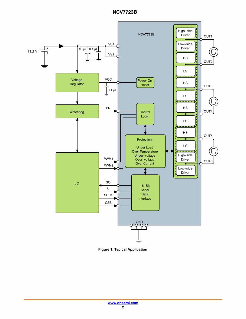
Figure 1. Typical Application
NCV7723BOUT1
OUT2
Low−sideDriver
High−sideDriver
LS
HS
OUT3
OUT4
LS
HS
LS
HS
OUT5
OUT6
LS
HS
Low−sideDriver
High−sideDriver
16−BitSerialData
Interface
Power OnReset
ControlLogic
SO
SI
SCLK
CSB
VCC
EN
uC
Watchdog
VoltageRegulator
VS1
GND
13.2 VVS2
PWM1
PWM2
10 �F 0.1 �F
0.1 �F
Protection:
Under LoadOver Temperature
Under−voltageOver−voltageOver Current

NCV7723B
www.onsemi.com3
ENABLE
BIASPOR
SPI and 16 Bit Logic Control
FaultReporting
EN
VCC
SO
SI
SCLK
CSB
VS1
DRIVE 2
ControlLogic Wave Shaping
Wave Shaping
Low SideDriver
High SideDriver
Fau
lt
HS+LS Under Load
Overcurrent
DRIVE1
OUT1
VS1
VS1 OUT2
VS2
VS
OvervoltageLockout
VS1,
GND
DRIVE 3VS2 OUT3
DRIVE 4VS2 OUT4
DRIVE 5VS1 OUT5
DRIVE 6VS2 OUT6
GNDGND
Thermal Warning &Shutdown
VS
GND
UndervoltageLockout
ChargePump
VS
PWM1
PWM2
Figure 2. Block Diagram
VS2
GND
OUT1
OUT5
NC
SI
VCC
SO
EN
NC
OUT6
OUT4
GND
GND
OUT2
NC
VS1
SCLK
CSB
PWM2
PWM1
VS2
NC
OUT3
GND
1
2
3
4
5
6
7
8
9
10
11
12 13
14
15
16
17
18
19
21
20
22
23
24
EPAD
Figure 3. Pinout – SSOP24 NB EP

NCV7723B
www.onsemi.com4
PIN FUNCTION DESCRIPTION The pin−out for the Half−Bridge Driver in SSOP24 NB EP package is shown in the table below.
Pin#SSOP24 Symbol Description
1 GND Ground. Must be connected to other GND pins externally.
2 OUT1 Half−bridge output 1
3 OUT5 Half−bridge output 5
4 NC No Connection. This pin should be isolated from any traces or via on the PCB board.
5 SI 16 bit serial communication input. 3.3 V / 5 V (TTL) Compatible − internally pulled down.
6 VCC Power supply input for Logic.
7 SO 16 bit serial communication output. 3.3 V / 5 V Compliant
8 EN Enable − active high; wakes the device from sleep mode. 3.3 V / 5 V (TTL) Compatible − internally pulled down.
9 NC No Connection. This pin should be isolated from any traces or via on the PCB board.
10 OUT6 Half−bridge output 6
11 OUT4 Half−bridge output 4
12 GND Ground. Must be connected to other GND pins externally.
13 GND Ground. Must be connected to other GND pins externally.
14 OUT3 Half−bridge output 3
15 NC No Connection. This pin should be isolated from any traces or via on the PCB board.
16 VS2 Power Supply input for outputs 3, 4, and 6. This pin must be connected to VS1 externally.
17 PWM1 External PWM input for output 1. 3.3 V / 5 V (TTL) Compatible − internally pulled down. Connect to ground or leave floating if unused.
18 PWM2 External PWM input for output 2. 3.3 V / 5 V (TTL) Compatible − internally pulled down. Connect to ground or leave floating if unused.
19 CSB Chip select bar − active low; enables serial communication operation. 3.3 V / 5 V (TTL) Compatible − internally pulled up.
20 SCLK Serial communication clock input. 3.3 V / 5 V (TTL) Compatible − internally pulled down.
21 VS1 Power Supply input for outputs 1, 2, and 5. This pin must be connected to VS2 externally.
22 NC No Connection. This pin should be isolated from any traces or via on the PCB board.
23 OUT2 Half−bridge output 2
24 GND Ground. Must be connected to other GND pins externally.
EPAD Exposed Pad Connect to GND or leave unconnected.
MAXIMUM RATINGS (Voltages are with respect to GND)
Rating Symbol Value Unit
VSx Pin Voltage (VS1, VS2)(DC)(AC), t < 500 ms, Ivsx > −2 A
VsxdcMaxVSxac
−0.3 to 45−1.0
V
Pin Voltage (Vcc, SI, SCLK, CSB, SO, EN, PWM1, PWM2) VioMax −0.3 to 5.5 V
OUTx Pin Voltage(DC)(AC)(AC), t < 500 ms, IOUTx > −1.1 A(AC), t < 500 ms, IOUTx < 1 A
VoutxDcVoutxAc
−0.3 to 45−0.3 to 45
−1.01.0
V
OUTx Pin Current (OUT1, ..., OUT6) IoutxImax −2.0 to 2.0 A
Junction Temperature Range TJ −40 to 150 °C
Storage Temperature Range Tstr −55 to 150 °C
Peak Reflow Soldering Temperature: Pb−free 60 to 150 seconds at 217°C (Note 1) 260 °C
Stresses exceeding those listed in the Maximum Ratings table may damage the device. If any of these limits are exceeded, device functionalityshould not be assumed, damage may occur and reliability may be affected.1. See or download onsemi’s Soldering and Mounting Techniques Reference Manual, SOLDERRM/D.
NCV7723B
www.onsemi.com5
ATTRIBUTES
Characteristic Symbol Value Unit
Short Circuit Reliability Characterization AECQ10x Grade A
ESD Capability Human Body Model per AEC−Q100−002 VSx, OUTx
All Other PinsCharged Device Model per AEC−Q100−011
Vesd4kVesd2k
Vesd750
≥ ±4.0 kV≥ ±2.0 kV≥ ±750 V
Moisture Sensitivity Level MSL MSL2
Package Thermal Resistance – Still−airJunction–to–Ambient (Note 2)Junction–to–Board (Note 2)
R�JAR�JBOARD
32.121.8
°C/W°C/W
2. Based on JESD51−7, 1.6 mm thick FR4, 2S2P PCB with 600 mm2 2 oz. copper and 18 thermal vias to 80x80 mm 1 oz. internal spreaderplanes. Simulated with each channel dissipating 0.2 W.
RECOMMENDED OPERATING CONDITIONS
Parameter Symbol Min Max Unit
Digital Supply Input Voltage VCCOp 3.15 5.25 V
Battery Supply Input Voltage (VS1 = VS2) VSxOp 5.5 32 V
DC Output Current IxOp − 0.5 A
Junction Temperature TjOp −40 125 °C
Functional operation above the stresses listed in the Recommended Operating Ranges is not implied. Extended exposure to stresses beyondthe Recommended Operating Ranges limits may affect device reliability.
ELECTRICAL CHARACTERISTICS (−40°C ≤ TJ ≤ 150°C, 5.5 V ≤ VSx ≤ 40 V, 3.15 V ≤ VCC ≤ 5.25 V, EN = VCC, unless otherwise specified.)
Characteristic Symbol Conditions Min Typ Max Unit
POWER SUPPLIES
Supply Current (VS1 + VS2) Sleep Mode
IqVSx85 VS1 = VS2 = 13.2 V, VCC = 0 V−40°C to 85°C − 1.0 2.5 �A
Supply Current (VS1 + VS2) Active Mode
IvsOp EN = VCC, 5.5V < VSx < 32 V No Load,All Outputs Off
−0.5 1.0 mA
Supply Current (Vcc) Sleep Mode
Active Mode
IqVCC
IVCCOp
CSB = VCC, EN = SI = SCLK = 0 V−40°C to 85°C
EN = CSB = VCC, SI = SCLK = 0 V No Load, All Outputs Off
−
−
1.0
1.5
2.5
3.0
�A
mA
Total Sleep Mode CurrentI(VS1) + I(VS2) + I(VCC)
IqTot Sleep Mode, −40°C to 85°C VS1 = VS2 = 13.2 V, No Load
− 2.0 5.0 �A
VCC Power−on Reset Threshold VCCpor VCC increasing − 2.70 2.90 V
VSx Undervoltage Detection Threshold VSxuv VSx decreasing VSx increasing
3.53.7
4.14.3
4.54.7
V
VSx Undervoltage Detection Hysteresis VSxuHys 100 − 450 mV
VSx Overvoltage Detection Threshold VsXov VSx increasing VSx decreasing
3229.5
3633.5
4037.5
V
VSx Overvoltage Detection Hysteresis VSxoHys − 2.5 − V
DRIVER OUTPUT CHARACTERISTICS
Output High RDS(on) (source) RDSonHS Iout = −500 mA, Vs = 13.2 V VCC = 3.15 V
− 0.8 1.8 �
Output Low RDS(on) (sink) RDSonLS Iout = 500 mA, Vs = 13.2 V VCC = 3.15 V
− 0.8 1.8 �
Source Leakage CurrentIsrcLkg13.2IsrcLkg28
VCC = 5 V, OUT (1−6) = 0 V, EN = 0/5 V VSx = 13.2 V VSx = 28 V
−1.0−2.0
−−
−−
�A�A

NCV7723B
www.onsemi.com6
ELECTRICAL CHARACTERISTICS (−40°C ≤ TJ ≤ 150°C, 5.5 V ≤ VSx ≤ 40 V, 3.15 V ≤ VCC ≤ 5.25 V, EN = VCC, unless otherwise specified.) (continued)
Characteristic UnitMaxTypMinConditionsSymbol
DRIVER OUTPUT CHARACTERISTICS
Sink Leakage CurrentIsnkLkg13.2IsnkLkg28
VCC = 5 V, EN = 0/5 V OUT (1−6) = VSx = 13.2 V OUT (1−6) = VSx = 28 V
−−
−−
1.02.0
�A�A
Overcurrent Shutdown Threshold (Source) IsdSrc VCC = 5 V, VSx = 13.2 V −2.0 −1.5 −1.1 A
Overcurrent Shutdown Threshold (Sink) IsdSnk VCC = 5 V, VSx = 13.2 V 1.1 1.5 2.0 A
Over Current Delay Timer TdOc 10 25 50 �s
Underload Detection Threshold (Low Side) IuldLS VCC = 5 V, VSx = 13.2 V − 2.5 7.5 mA
Underload Detection Threshold (High Side) IuldHS VCC = 5 V, VSx = 13.2 V −7.5 −2.5 − mA
Underload Detection Delay Time TdUld VCC = 5 V, VSx = 13.2 V 200 350 600 �s
Body Diode Forward Voltage IbdFwd If = 500 mA − 0.9 1.3 V
DRIVER OUTPUT SWITCHING CHARACTERISTICS
High Side Turn On Time ThsOn Vs = 13.2 V, Rload = 70 � − 120 165 �s
High Side Turn Off Time ThsOff Vs = 13.2 V, Rload = 70 � − 20 45 �s
Low Side Turn On Time TlsOn Vs = 13.2 V, Rload = 70 � − 120 165 �s
Low Side Turn Off Time TlsOff Vs = 13.2 V, Rload = 70 � − 35 75 �s
High Side Rise Time ThsTr Vs = 13.2 V, Rload = 70 � 10 30 50 �s
High Side Fall Time ThsTf Vs = 13.2 V, Rload = 70 � 10 30 50 �s
Low Side Rise Time TlsTr Vs = 13.2 V, Rload = 70 � 10 30 50 �s
Low Side Fall Time TlsTf Vs = 13.2 V, Rload = 70 � 10 30 50 �s
High Side Off to Low Side On Non−Overlap Time
ThsOffLsOn Vs = 13.2 V, Rload = 70 � 5 − − �s
Low Side Off to High Side On Non−Overlap Time
TlsOffHsOn Vs = 13.2 V, Rload = 70 � 5 − − �s
PWM High to High Side On Time ThsOnPWM Vs = 13.2 V, Rload = 70 � − 120 165 �s
PWM Low to High Side Off Time ThsOffPWM Vs = 13.2 V, Rload = 70 � − 20 45 �s
PWM High to Low Side On Time TlsOnPWM Vs = 13.2 V, Rload = 70 � − 120 165 �s
PWM Low to Low Side Off Time TlsOffPWM Vs = 13.2 V, Rload = 70 � − 35 75 �s
THERMAL RESPONSE
Thermal Warning Twr (Note 3) 120 140 170 °C
Thermal Warning Hysteresis TwHy (Note 3) − 20 − °C
Thermal Shutdown Tsd (Note 3) 150 175 200 °C
Thermal Shutdown Hysteresis TsdHy (Note 3) − 20 − °C
LOGIC INPUTS − EN, SI, SCLK, CSB, PWM1, PWM2
Input Threshold HighLow
VthInHVthInL
2.0−
−−
−0.6
VV
Input Hysteresis − SI, SCLK, CSB, PWM1, PWM2
VthInHys 50 150 300 mV
Input Hysteresis − EN VthENHys 150 400 800 mV
Pull−down Resistance − EN, SI, SCLK, PWM1, PWM2
Rpdx EN = SI = SCLK = VCC 50 125 200 k�
Pull−up Resistance − CSB RpuCSB CSB = 0 V 50 125 250 k�
Input Capacitance Cinx (Note 3) − − 15 pF

NCV7723B
www.onsemi.com7
ELECTRICAL CHARACTERISTICS (−40°C ≤ TJ ≤ 150°C, 5.5 V ≤ VSx ≤ 40 V, 3.15 V ≤ VCC ≤ 5.25 V, EN = VCC, unless otherwise specified.) (continued)
Characteristic UnitMaxTypMinConditionsSymbol
LOGIC OUTPUT − SO
Output High VsoH ISOURCE = −1 mA VCC –0.6
− − V
Output Low VsoL ISINK = 1.6 mA − − 0.4 V
Tri−state Leakage ItriStLkg CSB = 5 V −5 − 5 �A
Tri−state Output Capacitance ItriStCout CSB = VCC, 0 V < VCC < 5.25 V (Note 3) − − 15 pF
SERIAL PERIPHERAL INTERFACE
SCLK Frequency Fclk − − − 5.0 MHz
SCLK Clock Period TpClk VCC = 5 V VCC = 3.3 V −
200500
−−
−−
ns
SCLK High Time TclkH 1 85 − − ns
SCLK Low Time TclkL 2 85 − − ns
SCLK Setup Time TclkSup 3, 4 85 − − ns
SI Setup Time TsiSup 11 50 − − ns
SI Hold Time TsiH 12 50 − − ns
CSB Setup Time TcsbSup 5, 6 100 − − ns
CSB High Time TcsbH (Note 4) 7 5.0 − − �s
SO enable after CSB falling edge TenSo 8 − − 200 ns
SO disable after CSB rising edge TdisSo 9 − − 200 ns
SO Rise/Fall Time TsoR/F Cload = 40 pF (Note 3) − − 10 25 ns
SO Valid Time TsoV Cload = 40 pF (Note 3) SCLK ↑ to SO 50%
10 − 50 100 ns
EN Low Valid Time TenL VCC = 5 V; EN H → L 50% to OUTx turning off 50%
− 10 − − �s
EN High to SPI Valid TenHspiV − − − 100 �s
SRR Delay Between Consecutive Frames Tsrr (Note 5) − 150 − − �s
Product parametric performance is indicated in the Electrical Characteristics for the listed test conditions, unless otherwise noted. Productperformance may not be indicated by the Electrical Characteristics if operated under different conditions.3. Not production tested.4. This is the minimum time the user must wait between SPI commands.5. This is the minimum time the user must wait between consecutive SRR requests.

NCV7723B
www.onsemi.com8
CHARACTERISTIC TIMING DIAGRAMS
LS Turn OFF
HS Turn ON
CSB
TlsOff
TlsTr
ThsTr
TlsOffHsOn
ThsOn
HS Turn Off
LS Turn On
CSB
ThsOff
TlsOn
TlsTf
ThsTf
ThsOffLsOn
10%
10%
10%
10%
90%
90%
90%
90%
90%
90%
Figure 4. Detailed Driver Timing

NCV7723B
www.onsemi.com9
Figure 5. Detailed Driver Timing (OUT1 / OUT2 PWM)
HS Turn ON
PWMx
ThsTr
ThsOnPWM
HS Turn Off
LS Turn Off
PWMx ThsOffPWM
TlsOffPWM
TlsTr
ThsTf
10%
10%
10%
90%
90%
90%
90%
90%
LS Turn On
TlsOnPWM
90%
10%
TlsTf

NCV7723B
www.onsemi.com10
10
SI
SCLK
SO
11
12
CSB
SCLK
3 1 2
5
4 7
6
CSB
SO
8 9
Figure 6. Detailed SPI Timing

NCV7723B
www.onsemi.com11
TYPICAL PERFORMANCE GRAPHS
Figure 7. IqTot vs. Temperature Figure 8. I(VCC) Active Mode vs. V(VCC)
TEMPERATURE (°C) VCC VOLTAGE (V)
15050−500
0.5
1.5
2.0
3.0
3.5
5.55.04.54.03.53.01.20
1.24
1.26
1.28
1.32
Figure 9. RDS(on) vs. Temperature Figure 10. Body Diode vs. Temperature
TEMPERATURE (°C)
TEMPERATURE (°C)
Figure 11. Overcurrent vs. Temperature Figure 12. Leakage vs. Temperature
TEMPERATURE (°C)
TEMPERATURE (°C)
IqTo
t, T
OTA
L S
LEE
P M
OD
E C
UR
RE
NT
(�A
)
AC
TIV
E M
OD
E V
CC
CU
RR
EN
T (
mA
)
RD
S(o
n) (�
)
I src
Lkg,
I snk
Lkg
(�A
)B
OD
Y D
IOD
E F
OR
WA
RD
VO
LTA
GE
(V
)
1.0
2.5 VCC = 5.25 V
VCC = 5 V
VCC = 3.15 V1.22
1.30
150°C
−40°C
25°C
IsdS
rc, I
sdS
nk O
VE
RC
UR
RE
NT
(A
)
VSx = 13.2 VVSx = 13.2 V
150100500−500.6
0.8
1.0
1.2
1.4
1.6
1.8
150100500−500
0.02
0.04
0.06
0.08
0.1
0.12
0.14
150100500−500.75
0.8
0.85
0.9
1.0
150100500−501.2
1.3
1.5
1.6
1.7
0 100
VSx = 13.2 V
VSx = 13.2 VVCC = 5 V
Isnk
If = 0.5 A
HSx
LSx
1.4VSx = 13.2 VVCC = 5.0 V
HSx
LSx
1.34
1.36
1.40
1.38
HSx
LSx
0.95
Isrc
0.16
0.18
0.2

NCV7723B
www.onsemi.com12
DETAILED OPERATING DESCRIPTION
General OverviewThe NCV7723B is comprised of twelve NMOS power
drivers. The drivers are arranged as six half−bridge outputchannels, allowing for three independent full−bridgeconfigured loads. Output control and status reporting ishandled via the SPI (Serial Peripheral Interface)communications port. OUT1 and OUT2 can be controlledwith an external PWM signal.
Each output is characterized for a typical 0.5 A DC loadand has a maximum 2.0 A surge capability (at VSx =13.2 V). Maximum allowable junction temperature is150°C and may constrain the maximum load current and/orlimit the number of drivers active at once.
An active−high enable function (EN) allows globalcontrol of the outputs and provides a low quiescent currentsleep mode when the device is not being utilized. An internalpull−down resistor is provided on the input to ensure thedevice enters sleep mode if the input signal is lost.
After EN transitions from low to high, the VCC POR cyclewill proceed and bring the device into normal operation. Thedevice configuration registers can then be programmed viaSPI. Bringing EN low clears all registers (no configurationor status data is stored), disables the drivers, and enters sleepmode.
SPI Communication16−bit full duplex SPI communication has been
implemented for device configuration, driver control, andreading the status data. In addition to the 16−bit status data,a pseudo−bit (PRE_15) can also be retrieved from the SOoutput.
The device must be enabled (EN = H) for SPIcommunication. The SPI inputs are TTL compatible and theSO output high level is defined by the applied VCC. Theactive−low CSB input has a pull−up resistor and theremaining inputs have pull−down resistors to bias them toknown states when SPI communication is inactive.
The latched thermal shutdown (TSD) status bit PRE_15is available on SO until the first rising SCLK edge after CSBgoes low. The following conditions must be met for a validTSD read to be captured:
1. SCLK and SI are low before the CSB cycle;2. CSB transitions from high to low;3. CSB setup time (TcsbSup: Figure 6, #5) is
satisfied.Figure 13 shows the SPI communication frame format,
and Tables 1 and 2 define the command input and diagnosticstatus output bits.
Figure 13. SPI Communication Frame Format
PRE_15PSEUDO−BIT
OCS PSF ULDTSD TW
SRR HBSEL ULDSC
15 14 13 0
OVLO
CSB
SI
SCLK
SO B[12:7] → HBST[6:4]
B[12:7] → HBEN[6:1]
B[6:1] → HBST[3:1]
B[6:1] → HBCNF[6:1]
Communication is implemented as follows and is alsoillustrated in Figures 13 and 15:
1. SI and SCLK are set low before the CSB cycle.2. CSB goes low to begin a serial data frame;
pseudo−bit PRE_15 is immediately available atSO.
3. SI data is shifted in on every rising edge of SCLK,starting with the most significant bit (MSB), SRR.
4. SI data is recognized on every falling edge of theSCLK.
5. Current SO data is simultaneously shifted out onevery rising edge of SCLK, starting with the MSB(OCS).
6. CSB goes high to end the frame and SO becomestri−state.
7. The last 16 bits clocked into SI are transferred tothe device’s data register if no frame error isdetected, otherwise the entire frame is ignored andthe previous input data is preserved.

NCV7723B
www.onsemi.com13
Table 1. SPI COMMAND INPUT DEFINITIONS
Channels 6 – 1
Bit# Name Function Status* Scope
15 SRR Status Register Reset** 1 = Reset Global Status Reset
14 HBSEL*** Half Bridge Selection Reserved −
13 ULDSC Underload Shutdown Control 1 = Enabled Per Half−Bridge Operation
12 HBEN6 Enable Half−Bridge 6
0 = Hi−Z1 = Enabled Per Half−Bridge
11 HBEN5 Enable Half−Bridge 5
10 HBEN4 Enable Half−Bridge 4
9 HBEN3 Enable Half−Bridge 3
8 HBEN2 Enable Half−Bridge 2
7 HBEN1 Enable Half−Bridge 1
6 HBCNF6 Configure Half−Bridge 6
0 = LS On, HS Off1 = LS Off, HS On Per Half−Bridge
5 HBCNF5 Configure Half−Bridge 5
4 HBCNF4 Configure Half−Bridge 4
3 HBCNF3 Configure Half−Bridge 3
2 HBCNF2 Configure Half−Bridge 2
1 HBCNF1 Configure Half−Bridge 1
0 OVLO VSx Overvoltage Lockout 1 = Enabled Global Lockout
*All command input bits are set to 0 at VCC power−on reset.**Latched faults are cleared and outputs can be re−programmed if no fault exists after SRR asserted.***HBSEL enables channel group selection for family devices with more than 6 channels. In the NCV7723B it is recommended to set the HBSEL
bit to 0.

NCV7723B
www.onsemi.com14
Table 2. SPI STATUS OUTPUT DEFINITIONS
Channels 6 – 1
Bit# Name Function Status* Scope
PRE_15 TSD Latched Thermal Shutdown 1 = Fault Global Notification; Per Half−Bridge Operation
15 OCS Latched Overcurrent Shutdown 1 = Fault Global Notification; Per Half−Bridge Operation
14 PSFVS1 and/or VS2
Undervoltage or Overvoltage 1 = Fault Global Notification; Global Operation
13 ULD Underload Detect 1 = Fault Global Notification; Per Half−Bridge Operation
12HBST6[1:0] Half Bridge 6 Output Status
0x00b – OutputDisabled
0x01b − OCS0x10b − ULD
0x11b − OutputEnabled
Per Half−Bridge
11
10HBST5[1:0] Half Bridge 5 Output Status
9
8HBST4[1:0] Half Bridge 4 Output Status
7
6HBST3[1:0] Half Bridge 3 Output Status
5
4HBST2[1:0] Half Bridge 2 Output Status
3
2HBST1[1:0] Half Bridge 1 Output Status
1
0 TW Thermal Warning 1 = Fault Global Notification; Per Half−Bridge Operation
*All status output bits are set to 0 at Vcc power−on reset (POR).HBSTx[1:0] bits are priority encoded to provide the status information of each of the half−bridge outputs. Figure 14 shows the priority encodingstate diagram for the HBSTx[1:0] bits.
OCS
ULD
Output Enabled
“10”
Output Disabled
(default)
SRR = ‘1’Power On Reset
OverCurrent
UnderLoad
PWMx = ‘1’
Over
Current
PSF, TSDHBENx = ‘0’
Power On Reset
PSF
TSD
PSF
TSD
Figure 14. SO HBSTx [1:0] Priority Encoding State Diagram
*PSF Recovery: VSx rising above the undervoltage threshold or falling below the overvoltage threshold (OVLO = 1)**TSD Recovery: Sending SRR after junction temperature has fallen below the thermal shutdown threshold
“11”
“01”
“00”
PSF Recovery*TSD Recovery**
HBENx = ‘1’

NCV7723B
www.onsemi.com15
Priority EncodingIf an under load event precedes an over current event on
the same half−bridge, the device will report HBSTx = ‘10’and then HBSTx = ‘01’ as shown in Figure 14. An overcurrent event preceding an under load event will reportHBSTx = ‘01’ since there is no direct path from the OCSstate to the ULD state. Thus an over current shutdown faultmust be cleared before an underload fault is reported on thesame half−bridge.
Frame Error DetectionThe NCV7723B employs frame error detection to help
ensure input data integrity. SCLK is compared to an n x 8 bitcounter and a valid frame (CSB H−L−H cycle) has integermultiples of 8 SCLK cycles. For the first 16 bits shifted intoSI, SCLK is compared to a modulo16 counter (n = 2), andSCLK is compared to a modulo 8 counter (n = 1, 2, ...m)thereafter. This variable modulus allows for daisy chainoperation with devices using different word lengths.
The last 16 bits clocked into SI are transferred to theNCV7723B’s data register if no frame error is detected,otherwise the entire frame is ignored and the previous inputdata is preserved.
Daisy Chain OperationDaisy chain operation is possible with multiple 16−bit and
8−bit devices that have a compatible SPI protocol. The clockphase and clock polarity with respect to the data for all thedevices in the chain must be the same as the NCV7723B.
CSB and SCLK are parallel connected to every device inthe chain while SO and SI are series connected between eachdevice. The master’s MOSI is connected to the SI of the firstdevice and the first device’s SO is connected to the nextdevice’s SI. The SO of the final device in the chain isconnected to the master’s MISO.
The hardware configuration for the NCV7723B daisychained with an 8−bit SPI device is shown in Figure 15.A 24−bit frame made of 16−bit word ‘A’ and 8−bit word ‘B’is sent from the master. Command word B is sent firstfollowed by word A. The master simultaneously receivesstatus word B first followed by word A. The progression ofdata from the MCU through the sequential devices isillustrated in Figure 15.
Compliance with the illustrated frame format is requiredfor proper daisy chain operation. Situations should beavoided where an incorrect multiple of 8 bits is sent to thedevices, but the frame length does not cause a frame error inthe devices. For example, the word order could beinadvertently interleaved or reversed. Invalid data isaccepted by the NCV7723B in such scenarios and possiblyby other devices in the chain, depending on their frame errorimplementation. Data is received as a command by thedevice at the beginning of the chain, but the device at the endof the chain may receive status data from the precedingdevice as a command.
NCV7723B16−bit Device
CSB
SCLK
SI SO
8−bit Device
CSB
SCLK
SI SO
Device BDevice A
CMD [B, 8]+
CMD [A, 16]
STA [A, 16]+
CMD [B, 8]+
MCU
CSB
SCLK
MISO
Master
MOSI
Figure 15. Daisy Chain Configuration
STA [A, 16]
STA [B, 8]
CMD [x, n] = Command Word to Device ‘x’, Length ‘n’STA [x, n] = Status Word from Device ‘x’, Length ‘n’

NCV7723B
www.onsemi.com16
Figure 16. Daisy Chain – 24 bit Frame Format
SCLK
CSB
SI
7 6 1 0 15
Word B − 8 bits Word A − 16 bits
24 bit Frame
TSDSO MSB
MSB
LSB
LSB
MSB
MSB
0
LSB
LSB
8 7
SI data is recognized on the falling SCLK. edge
SO data is shifted out on the rising SCLK edge.Modulo 16 counter begins on the first rising SCLK edge after CSB goes low.
Modulo 16 counter ends − 16 bit word length valid.Modulo 8 counter begins on the next rising SCLK edge.
Modulo 8 counter ends − 8 bit word length valid. valid n*8 bit frame.
TSD Bit in Daisy Chain OperationThe SO frame is designed to allow TSD status retrieval in
a daisy chain configuration using NCV7723B or otherdevices with identical SPI functionality. The TSD status bitis OR’d with SI and then multiplexed with the device’s usualstatus data (Figure 17).
CSB is held high and SI and SCLK are held low by themaster before the start of the SPI frame. TSD status isimmediately available as bit PRE_15 at SO (SO = TSD)when CSB goes low to begin the frame. The usual status data(SO = STA) becomes available after the first rising SCLKedge.
The TSD status automatically propagates through thechain from the SO output of the previous device to the SIinput of the next. This is shown in Figures 18 and 19, firstwithout a TSD fault in either device (Figure 18), and thensubsequently with a latched TSD fault (TSD = 1) in device“A” propagating through to device “B” (Figure 19).
Since the TSD status of any device propagatesautomatically through the entire chain, it is not possible todetermine which device (or devices) has a fault (TSD = 1).The usual status data from each device will need to beexamined to determine where a fault (or faults) may exist.
MUX
SO
SI
TSD
SPISI
SEL
SO
Figure 17. TSD SPI Link
NCV7726Bor NCV7723B
NCV7723B
CSB
SCLK
SI SO
CSB
SCLK
SI SO
Device BDevice A
0
MCU
CSB
SCLK
MISO
Master
MOSI0
No TSD No TSD
Figure 18. Daisy Chain Without TSD Fault
Z → 0
1 → 0
Z → 0

NCV7723B
www.onsemi.com17
NCV7726B
or NCV7723B
NCV7723B
CSB
SCLK
SI SO
CSB
SCLK
SI SO
Device BDevice A
0
MCU
CSB
SCLK
MISO
Master
MOSI0 Z → 1
Latched TSD No TSD
Figure 19. Daisy Chain With TSD Fault
1 → 0
Z → 1
Power Up/Down ControlThe VCC supply input powers the device’s logic core. A
VCC power−on reset (POR) function provides controlledpower−up/down. VCC POR initializes the command inputand status output registers to their default states (0x00), andensures that the bridge output and SO drivers maintain Hi−Zas power is applied. SPI communication and normal deviceoperation can proceed once VCC rises above the PORthreshold and EN remains high.
The VS1 and VS2 supply inputs power their respectiveoutput drivers (refer to Figure 2 and the PIN FUNCTIONDESCRIPTION). The VSx inputs are monitored to ensurethat the supply stays within the recommended operatingrange. If the VSx supply moves into either of the VSundervoltage or overvoltage regions, the output drivers areswitched to Hi−Z but command and status data is preserved.Output drivers will remain on if OVLO = 0 during anovervoltage condition.
Driver ControlThe NCV7723B has the flexibility to control each
half−bridge driver channel via SPI. Actual driver outputstate is determined by the command input and the currentfault status bits.
High−side (HSx) and low−side (LSx) drivers of the samechannel cannot be active at the same time, and non−overlapdelays are imposed when switching between HSx and LSxdrivers in the same channel, preventing currentshoot−through.
After the device has powered up and the drivers areallowed to turn on, the drivers remain on until commandedoff via SPI or until a fault condition occurs.
PWM ControlOutputs 1 and 2 can be controlled in two ways: through
normal SPI control (see Table 1) or from an external PWMsignal. OUT1 can be turned on/off using the HBEN1 bit or
applying a logic level signal to pin 17 (PWM1). OUT2 canbe turned on/off using the HBEN2 bit or applying a logiclevel signal to pin 18 (PWM2). Simplified logic functionsare shown below in Figure 20.
PWM Example: Turn on OUT1 High SideTo use OUT1 High Side with external PWM control,
perform the following steps:1. Send command 0b0000000000000010 (0x0002)
♦ Configures OUT1 to High Side (HBCNF1)♦ Disables OUT1 SPI Enable (HBEN1)
2. Apply logic level PWM signal to PWM1To use OUT1 Low Side with external PWM, set the
HBCNF1 bit to 0 during step 1.
HSx
LSx
VS
OUTx
GND
HBCNFx
HBENx
PWMx
PWMx HBENx HBCNFx HSx LSx OUTx
0 0 x OFF OFF Z
x 1 0 OFF ON Low
x 1 1 ON OFF High
1 x 0 OFF ON Low
1 x 1 ON OFF High
Figure 20. PWM Control Logic

NCV7723B
www.onsemi.com18
DIAGNOSTICS, PROTECTIONS, STATUS REPORTING AND RESET
OverviewThe NCV7723B employs diagnostics designed to prevent
destructive overstress during a fault condition. Diagnosticsare classified as either supervisory or protection functions(Table 3). Supervisory functions provide status informationabout device conditions. Protection functions provide statusinformation and activate fault management behaviors.Diagnostics resulting in output shutdown and latched statusmay depend on a qualifier and may require user interventionfor output recovery and status memory clear. Diagnosticsresulting in output lockout and non−latched status (VSOVor VSUV) may recover and clear automatically. Outputconfigurations can be changed during output lockout.Outputs assume the new configurations or resume theprevious configurations when an auto−recover fault is
resolved. Table 4 shows output states during faults andoutput recovery modes, and Table 5 shows the statusmemory and memory clear modes.
Table 3. DIAGNOSTIC CLASSES AND FUNCTIONS
Name Class Function
TSD Protection Thermal Shutdown
OCS Protection Overcurrent Shutdown
PSF Protection Under/overvoltage Lockout(OVLO = 1)
ULD Protection Underload Shutdown
HBSTx[1:0] Supervisory Half−Bridge X Output Status
TW Supervisory Thermal Warning
Table 4. OUTPUT STATE VS. FAULT AND OUTPUT RECOVERY
Fault Qualifier OUTx State OUTx Recovery OUTx Recovery Scope
TSD − → Z Send SRR All Outputs
OCS − → Z Send SRR All Outputs
PSF – VSOV OVLO = 1 → Z → Yn | Yn+1 Auto* All Outputs
OVLO = 0 Unaffected − −
PSF – VSUV − → Z → Yn | Yn+1 Auto* All Outputs
ULD ULDSC = 1 → Z Send SRR All Outputs
ULDSC = 0 Unaffected − −
TW − Unaffected − −
*OUTx returns to its previous state (Yn) or new state (Yn+1) if fault is removed.
Table 5. STATUS MEMORY VS. FAULT AND MEMORY CLEAR
Fault Qualifier Status Memory Memory Clear Memory Clear Scope
TSD − Latched Send SRR Global
OCS − Latched Send SRR Global
PSF – VSOV OVLO = X Non−Latched Auto* Global
PSF – VSUV − Non−Latched Auto* Global
ULD ULDSC = X Latched Send SRR Global
TW − Non−Latched Auto* Global
*Status memory returns to its no−fault state if fault is removed.
Status Information RetrievalCurrent status information is retrieved during each SPI
frame. To preserve device configuration and output states,the previous SI data pattern must be sent during the statusretrieval frame.
Status information is prevented from being updatedduring a SPI frame but new status becomes available afterCSB goes high at the end of the frame provided the frame didnot contain an SRR request. Status information includesboth global and per channel fault notification. To determinethe channel(s) affected after detecting a global fault,examine driver output status and input configuration.
Status Register Reset − SRRSending SRR = 1 clears status memory and re−activates
faulted outputs for all channels. The previous SI data patternmust be sent with SRR to preserve device configuration andoutput states.
At the rising edge of CSB, the SRR function is activatedand an internal timer (Tsrr) is started. Tsrr is the minimumtime the user must wait between consecutive SRR requests.If a fault is still present when SRR is sent, protection will bere−engaged and shutdown will recur. The status registers canalso be reset by toggling the EN pin or by VCC power−onreset.

NCV7723B
www.onsemi.com19
Diagnostics Details
The following sections describe individual diagnosticsand behaviors. In each description and illustration, a SPIframe is assumed to always be valid and the SI data patternsent for HBCNFx and HBENx is the same as the previousframe. Actual results can depend on asynchronous faultevents and SPI clock frequency and frame rate.
Undervoltage Lockout
Global Notification, Global OperationUndervoltage detection and lockout control is provided
by monitoring the VS1, VS2 and VCC supply inputs.Undervoltage hysteresis is provided to ensure clean
detection transitions. Undervoltage timing is shown inFigure 21.
Undervoltage at either VSx input turns off all outputs andsets the power supply fail (PSF) status bit. The outputs returnto their previously programmed state and the PSF status bitis cleared when VSx rises above the hysteresis voltage level.SPI communication is available and programmed outputenable and configuration states are maintained if properVCC is present during VSx undervoltage. Output enable andconfiguration states can also be programmed during VSxundervoltage if proper VCC is present, and state changeswill take effect as VSx rises above the undervoltagethreshold level.
OUTxLS
?
OUTxLS
?
XNo
Fault
OUTxLS
PSF
ALLZ
OUTxLS
NoFault
0x00
ALLZ
VSx
Vcc
?
OUTxHS
OUTxHS
VSUV
VccUV
No Fault PSF NoFault
0x00
OUTx VS
NoFault
OUTxHS
NoFault
t
OUTx GND OUTx GND
SI
Status
OutputState
SO Z
Figure 21. Undervoltage Timing
Overvoltage Lockout
Global Notification, Global OperationOvervoltage detection and lockout control is provided by
monitoring the VS1 and VS2 supply inputs. Hysteresis isprovided to ensure clean detection transitions. Overvoltagetiming is shown in Figure 22. Overvoltage at either VSxinput turns off all outputs if the overvoltage lockout input bitis set (OVLO = 1) and sets the power supply fail (PSF) statusbit (see Tables 4 and 5). The outputs return to theirpreviously programmed state and the PSF status bit iscleared when VSx falls below the hysteresis voltage level.
Output enable and configuration states can also beprogrammed during an overvoltage lockout event but willnot change state until VSx falls below the overvoltagethreshold level.
NOTE: to reduce stress, it is recommended to operate thedevice with OVLO bit asserted to ensure that thedrivers turn off during a load dump scenario. IfOVLO = 0 during an overvoltage condition,outputs will remain on and the PSF status bit willbe set.

NCV7723B
www.onsemi.com20
Figure 22. Overvoltage Timing
?
?
OUTxON
PSF
ALLZ
VSxVSOV
PSFNo
FaultNo
Fault
t
SI
Status
OutputState
SO
OUTx ONOVLO = 0
X
OUTxON
NoFault
NoFault
OUTxON
OUTx ONOVLO = 1
NoFault
VSOV
PSF
PSF
OUTxON
OUTxON
NoFault
OUTxOFF
NoFault
OUTx Z
Overcurrent Shutdown
Global and per Channel NotificationPer Half−Bridge Operation
Overcurrent detection and shutdown control is providedby monitoring each HS and LS driver. Overcurrent timing isshown in Figure 23. Overcurrent in either driver starts achannel’s overcurrent delay timer (TdOc). If overcurrentexists after the delay, both drivers are latched off and the
global overcurrent (OCS) status bit is set. The channel’scorresponding HBSTx[1:0] bits are also set to “01” toindicate an OCS fault. Note that OCS fault reporting haspriority over other faults as shown in Figure 14. The globalOCS bit and individual channel bits are cleared and channelsare re−activated by sending SRR = 1.
A persistent overcurrent cause should be resolved prior tore−activation to avoid repetitive stress on the drivers.
Figure 23. Overcurrent Timing
OUTxON
OCS
IsdSxx
t
SI
Status
OutputState
SO
OUTx ONSRR = 0
OUTxON
NoFault
OUTx ONSRR = 1
OUTxON
OUTx Z
OutputCurrent
OUTxON
NoFault
NoFault
TdOc
OCS
OUTx Z
TdOc
OUTxON
NoFault
NoFault
OUTxON
OCS
OCS
OCS

NCV7723B
www.onsemi.com21
Underload Shutdown
Global and per Channel NotificationGlobal Shutdown Control, Per Half−Bridge Operation
Underload detection and shutdown control is provided bymonitoring each half bridge driver. Underload timing isshown in Figure 24. Underload at any driver starts the globalunderload delay timer. If underload occurs in anotherchannel after the global timer has been started, the delay forany subsequent underload will be the remainder of the timer.
If underload exists after the global delay timer and if theunderload shutdown (ULDSC) command bit is set, bothHSand LS drivers are latched off and the global underload
(ULD) status bit is set along with the corresponding perchannel status bits HBSTx[1:0] set to “10”. Drivers willremain on if the ULDSC input bit is 0 (see Table 4 and 5).The global ULD bit and per channel HBSTx bits are clearedand channels are re−activated by sending SRR = 1.
NOTE: underload may result from a fault (e.g. open−load)condition or normal circuit behavior (e.g. L/Rtau). In motor applications it is often desirable toactively brake the motor by turning on both HS orLS drivers in two half−bridge channels which mayresult in an underload condition as current decays.
Figure 24. Underload Timing
SI
Status
OutputState
SO
OutputCurrent
t
LSx ONULDSC = 0
LSxON
NoFault
LSx ONSRR = 1
NoFault
NoFault ULD
OUTxON
No Fault
ULD
ULD
LSx ONULDSC = 1
ULD
LSx ONSRR = 1
LSxON
ULD
OUTx GND
IuldLS
TdUld TdUld
OUTxZ
OUTx GND
No FaultNoFault
TdUld

NCV7723B
www.onsemi.com22
Thermal Warning and Thermal Shutdown
Global Notification, Per Half−Bridge OperationThermal warning (TW) and thermal shutdown (TSD)
detection and control are provided for each half−bridge bymonitoring the driver pair’s thermal sensor. Thermalhysteresis is provided for each of the warning and shutdownfunctions to ensure clean detection transitions. Softwarepolling of the TW bit allows for avoidance of thermalshutdown since TW notification precedes TSD notification.Thermal warning and shutdown timing is shown inFigure 25.
The TW status bit is set when a half−bridge’s sensortemperature exceeds the warning level (TJ > Twr), and thebit is automatically cleared when sensor temperature fallsbelow the warning hysteresis level (TJ < TwHy). A channel’soutput state is unaffected by TW.
When sensor temperature exceeds the shutdown level(TJ > Tsd), the channel’s HS and LS drivers are latched off,the TW bit is/remains set, and the TSD (PRE_15) bit is set.The TSD bit is cleared and all affected channels arere−activated (TJ < TsdHy) by sending SRR = 1.
Figure 25. Thermal Warning and Shutdown Timing
OUTxON
t
SI
Status
OutputState
SO
OUTxON
NoFault
TSD
TWR
TJ
TWNo
Fault TW
OUTx ON
NoFault
NoFault
OUTxON
TW
OUTxON
TW
OUTx Z
TwHy
TsdHy
OUTx ONSRR = 1
TSDTW
TSDTW TW
OUTx ONSRR = 1
TW
OUTxON
TW
The latched thermal shutdown (TSD) information isavailable on SO after CSB transitions from high to low andbefore the first rising SCLK edge. The following proceduresmust be met for a true TSD reading:
1. SCLK and SI are low before the CSB cycle.Violating these conditions will results in an
undetermined SPI behavior or/and an incorrectTSD reading.
2. CSB transitioning from high to low.3. CSB setup time (TcsbSup) is satisfied and the data
is captured before the first SCLK rising edge.
NCV7723B
www.onsemi.com23
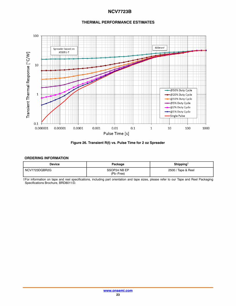
THERMAL PERFORMANCE ESTIMATES
Figure 26. Transient R(t) vs. Pulse Time for 2 oz Spreader
ORDERING INFORMATION
Device Package Shipping†
NCV7723DQBR2G SSOP24 NB EP(Pb−Free)
2500 / Tape & Reel
†For information on tape and reel specifications, including part orientation and tape sizes, please refer to our Tape and Reel PackagingSpecifications Brochure, BRD8011/D.

ÉÉÉÉÉÉ
SSOP24 NB EPCASE 940AK
ISSUE ODATE 24 APR 2012
SCALE 1:1
DIM MIN MAXMILLIMETERS
A 1.70A1 0.00 0.10
L 0.40 0.85
e 0.65 BSC
c 0.09 0.20
h 0.25 0.50
b 0.19 0.30
L2 0.25 BSCM 0 8 � �
NOTES:1. DIMENSIONING AND TOLERANCING PER ASME
Y14.5M, 1994.2. CONTROLLING DIMENSION: MILLIMETERS.3. DIMENSION b DOES NOT INCLUDE DAMBAR
PROTRUSION. DAMBAR PROTRUSION SHALLBE 0.10 MAX. AT MMC. DAMBAR CANNOT BELOCATED ON THE LOWER RADIUS OF THEFOOT. DIMENSION b APPLIES TO THE FLATSECTION OF THE LEAD BETWEEN 0.10 TO 0.25FROM THE LEAD TIP.
4. DIMENSION D DOES NOT INCLUDE MOLDFLASH, PROTRUSIONS OR GATE BURRS. MOLDFLASH, PROTRUSIONS OR GATE BURRS SHALLNOT EXCEED 0.15 PER SIDE. DIMENSION D ISDETERMINED AT DATUM PLANE H.
5. DIMENSION E1 DOES NOT INCLUDE INTERLEADFLASH OR PROTRUSION. INTERLEAD FLASHOR PROTRUSION SHALL NOT EXCEED 0.25 PERSIDE. DIMENSION E1 IS DETERMINED AT DA-TUM PLANE H.
6. DATUMS A AND B ARE DETERMINED AT DATUMPLANE H.
7. A1 IS DEFINED AS THE VERTICAL DISTANCEFROM THE SEATING PLANE TO THE LOWESTPOINT ON THE PACKAGE BODY.
8. CONTOURS OF THE THERMAL PAD ARE UN-CONTROLLED WITHIN THE REGION DEFINEDBY DIMENSIONS D2 AND E2.
PIN 1REFERENCE
0.10SEATINGPLANE
24X be
DETAIL A
---
SOLDERING FOOTPRINT
L
L2GAUGE
DETAIL A
E1 3.90 BSC
PLANE
SEATINGPLANEC
c
h
END VIEW
A-BM0.12 DCTOP VIEW
SIDE VIEW
A-B0.20 C
1 12
24A
B
D
2X 12 TIPS
A1
A2
C
C24X
D 8.64 BSC
E 6.00 BSC
24X1.15
24X0.40 0.65
DIMENSIONS: MILLIMETERS
PITCH
6.40
1
2X
A
M
13
0.20 C
0.20 C2X
0.10 C
RECOMMENDED
A2 1.651.10
GENERICMARKING DIAGRAM*
XXXXXXXXXGAWLYYWW
XXXX = Specific Device CodeA = Assembly LocationWL = Wafer LotYY = YearWW = Work WeekG = Pb−Free Package
(Note: Microdot may be in either location)
EE1
D
NOTE 5
NOTE 6
NOTE 6
NOTE 4
A-BM0.15 DC
BOTTOM VIEW
E2
NOTE 8
D2
NOTE 8
A-BM0.15 DC
2.84
5.63
D2 5.28 5.58
E2 2.44 2.64
L1 1.00 REF
H
A1
NOTE 7
L1
h
*This information is generic. Please refer todevice data sheet for actual part marking.Pb−Free indicator, “G” or microdot “�”, mayor may not be present. Some products maynot follow the Generic Marking.
MECHANICAL CASE OUTLINE
PACKAGE DIMENSIONS
ON Semiconductor and are trademarks of Semiconductor Components Industries, LLC dba ON Semiconductor or its subsidiaries in the United States and/or other countries.ON Semiconductor reserves the right to make changes without further notice to any products herein. ON Semiconductor makes no warranty, representation or guarantee regardingthe suitability of its products for any particular purpose, nor does ON Semiconductor assume any liability arising out of the application or use of any product or circuit, and specificallydisclaims any and all liability, including without limitation special, consequential or incidental damages. ON Semiconductor does not convey any license under its patent rights nor therights of others.
98AON79998EDOCUMENT NUMBER:
DESCRIPTION:
Electronic versions are uncontrolled except when accessed directly from the Document Repository.Printed versions are uncontrolled except when stamped “CONTROLLED COPY” in red.
PAGE 1 OF 1SSOP24 NB EP
© Semiconductor Components Industries, LLC, 2019 www.onsemi.com

onsemi, , and other names, marks, and brands are registered and/or common law trademarks of Semiconductor Components Industries, LLC dba “onsemi” or its affiliatesand/or subsidiaries in the United States and/or other countries. onsemi owns the rights to a number of patents, trademarks, copyrights, trade secrets, and other intellectual property.A listing of onsemi’s product/patent coverage may be accessed at www.onsemi.com/site/pdf/Patent−Marking.pdf. onsemi reserves the right to make changes at any time to anyproducts or information herein, without notice. The information herein is provided “as−is” and onsemi makes no warranty, representation or guarantee regarding the accuracy of theinformation, product features, availability, functionality, or suitability of its products for any particular purpose, nor does onsemi assume any liability arising out of the application or useof any product or circuit, and specifically disclaims any and all liability, including without limitation special, consequential or incidental damages. Buyer is responsible for its productsand applications using onsemi products, including compliance with all laws, regulations and safety requirements or standards, regardless of any support or applications informationprovided by onsemi. “Typical” parameters which may be provided in onsemi data sheets and/or specifications can and do vary in different applications and actual performance mayvary over time. All operating parameters, including “Typicals” must be validated for each customer application by customer’s technical experts. onsemi does not convey any licenseunder any of its intellectual property rights nor the rights of others. onsemi products are not designed, intended, or authorized for use as a critical component in life support systemsor any FDA Class 3 medical devices or medical devices with a same or similar classification in a foreign jurisdiction or any devices intended for implantation in the human body. ShouldBuyer purchase or use onsemi products for any such unintended or unauthorized application, Buyer shall indemnify and hold onsemi and its officers, employees, subsidiaries, affiliates,and distributors harmless against all claims, costs, damages, and expenses, and reasonable attorney fees arising out of, directly or indirectly, any claim of personal injury or deathassociated with such unintended or unauthorized use, even if such claim alleges that onsemi was negligent regarding the design or manufacture of the part. onsemi is an EqualOpportunity/Affirmative Action Employer. This literature is subject to all applicable copyright laws and is not for resale in any manner.
PUBLICATION ORDERING INFORMATIONTECHNICAL SUPPORTNorth American Technical Support:Voice Mail: 1 800−282−9855 Toll Free USA/CanadaPhone: 011 421 33 790 2910
LITERATURE FULFILLMENT:Email Requests to: [email protected]
onsemi Website: www.onsemi.com
Europe, Middle East and Africa Technical Support:Phone: 00421 33 790 2910For additional information, please contact your local Sales Representative
◊


