NETWORK ON CHIP ROUTER
Students : Itzik Ben - shushanJonathan Silber
Instructor : Isaschar Walter
Final presentationFinal presentationpart Apart A
Winter 2006
NoC concept Design architecture Architecture logic implementation Design simulation What’s left to do...
AgendaAgenda

Problem:Power, size and performance not practical for multi-processor chips using a single bus
interconnection .
Solution:Network on Chip, based interconnection:
fast, reliable data and low power consumption.
Implement a router for NoC in VHDL based upon research made by facultymembers.
Design and implement interface unit between NoC routers and process units.
Design and implement an application of multi processing units using a Network on Chip based interconnection.
Project Goals

Network SchematicProcessing
Unit
NoC
ROUTERROUTERROUTER
ROUTER ROUTER ROUTER
ROUTER ROUTER ROUTER
InterfaceInterface
Interface
Interface Interface
Interface InterfaceInterface
Interface
Network problems
Transmitting large data (buffer size, latency)
Loss of data due to full buffer Data priorityData from several inputs to one outputBlocked path prevents data transmission

Data in network
Packet based data flow
Single-flit or multi-flit packets (wormhole)
Service level support (packet priority)
Virtual channel support (router feature)

Packets in Wormholearchitecture
Packet body Target Address
Command
A whole Packet
Each Packet is divided to Several smaller segments (flits)
Each flit is several bit width
Interface
Process
Unit
Process
Unit
Process
Unit
Process
Unit
Process
Unit
Processing
Unit
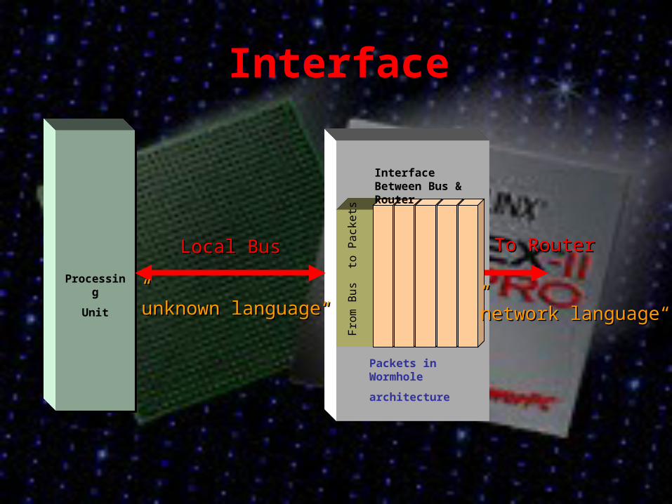
Interface Between Bus & Router
Packets in Wormhole
architecture
Fro
m B
us
to
Pa
cke
ts
To RouterTo RouterLocal BusLocal Bus
““network languagenetwork language””““unknown languageunknown language””

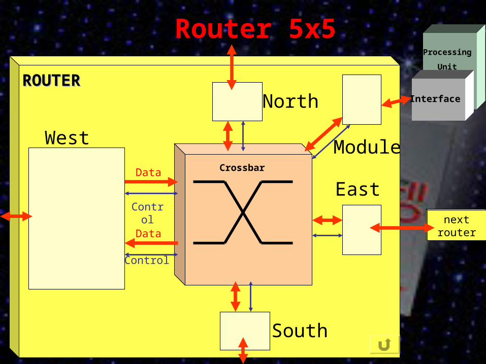
Router 5x5 Processing
Unit
Data
Control
Data
Control
ROUTERROUTER
CrossbarInput port
West
East
South
North
Processing
Unit
Interface
Module
output port
next router

Flit structure
one flit
Type
Service Level
Data out
x 2bit
x 2bit
x 12bitOr
8bit – first flitof packet
CRT)first flit
of packet(
x 4bit)network size
factor (
Lsb bit
Msb bit

4 msb bits of every flit
Service Level (SL):
Block Transfer = “00”(unimplemented yet)
Real-Time = “01”(unimplemented yet)
RD/WR = “10” (implemented as SL2)
Signaling = “11”(implemented as SL1)
Data Type:
Idle = “00” – no signal
Body = “01” – middle/header flit of a packet
EP = “10” – end of packet
FP = “11” – full packet (single flit packet)

Router designarchitecture guidelines
Input port serves as register-buffer
Crossbar designed in a full-connectivity (all inputs to all output)
Output port recognizes data waiting in input port buffer to be delivered, and extracts it (read command from output port goes to one or more inputs)

Routing Control & Terminology Each Service Level (SL) has an independent path from
input port until output port buffer
According to Current Routing Table (CRT) data is channeled to the appropriate output port, via the crossbar
In each output port the Current Serviced Input Port (CSIP) is determined by a Round-Robin logic which arbitrates between input ports waiting for transmission
Next Buffer’s State (NBS) determines if next router is ready to receive data

Router Input Port
FIFO
FIFO
ROUTERROUTER
InputInputPortPort
CRT
CRT
CRT
Sw
itch
ing
S
L
Data In flits
PR
EV
IOU
S R
OU
TE
R I
N P
AT
H
PR
EV
IOU
S R
OU
TE
R I
N P
AT
H //
PR
OC
ES
SIN
G U
NIT
PR
OC
ES
SIN
G U
NIT
Buffer credits read/writeControl
Crossbar
Data PerService-
Level
Current Routing Table
SL
Read linesFrom output- ports
To Output
Port
From
Input
Port
Routing DATA according to
CRT
From Input Port
To Output
port
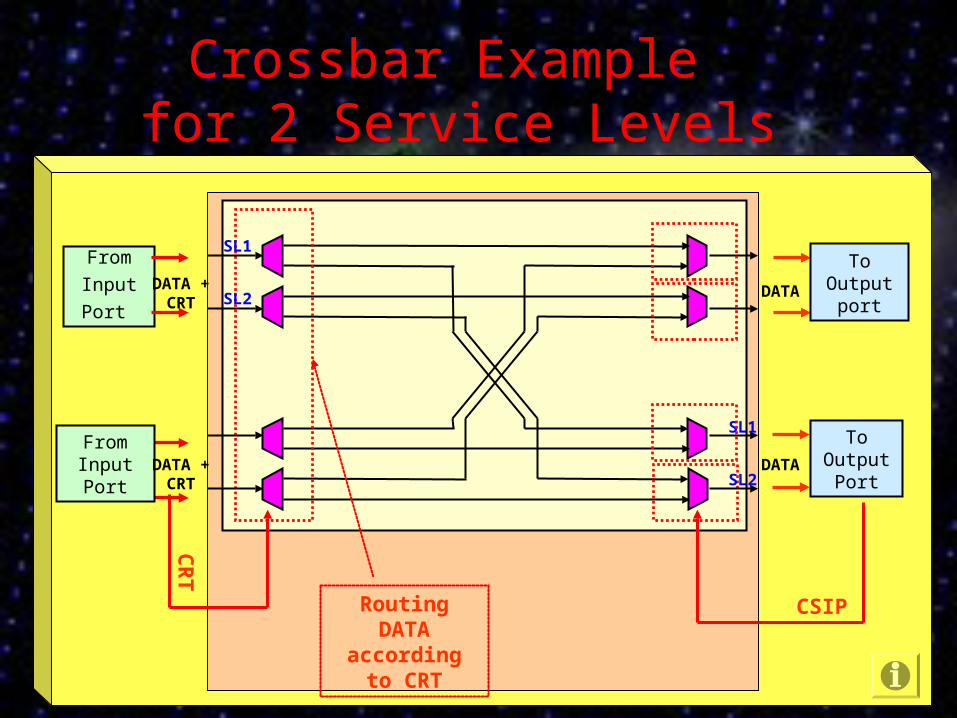
Crossbar Example for 2 Service Levels
DATA + CRT
DATA
DATADATA + CRT
CSIP
SL1
SL2
SL1
SL2
CR
T

Router Output Port
ROUTERROUTER
OutputOutputPortPort
CSIP
Buffer credits
NBS
CSIP
NBS
CSIP
Buffer credits Round-Robin
&control
NE
XT
RO
UT
ER
IN
PA
TH
N
EX
T R
OU
TE
R I
N P
AT
H //
PR
OC
ES
SIN
G U
NIT
PR
OC
ES
SIN
G U
NIT
Data In flits
Sw
itch
ing
S
L
Crossbar
Currently Serviced Input Port
Next Buffer State
Data PerService-
Level
Read linesTo input- ports
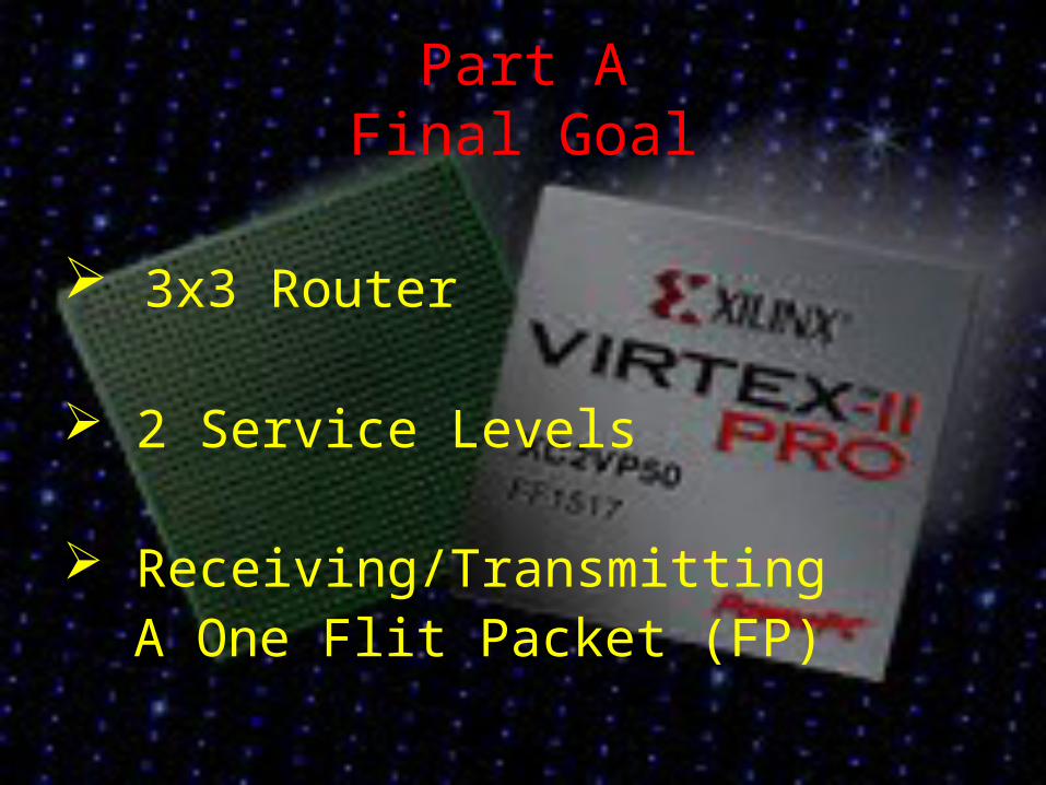
Part AFinal Goal
3x3 Router
2 Service Levels
Receiving/Transmitting A One Flit Packet (FP)


Final Router DesignPart A
Modular 5x5 Router, 16 bit data width
2 Service Levels (SL1, SL2)
Receiving/Transmitting Multi-flit packets (not only FP*)
* FP = Full-Packets

Top view:
Input port
output port
crossbar
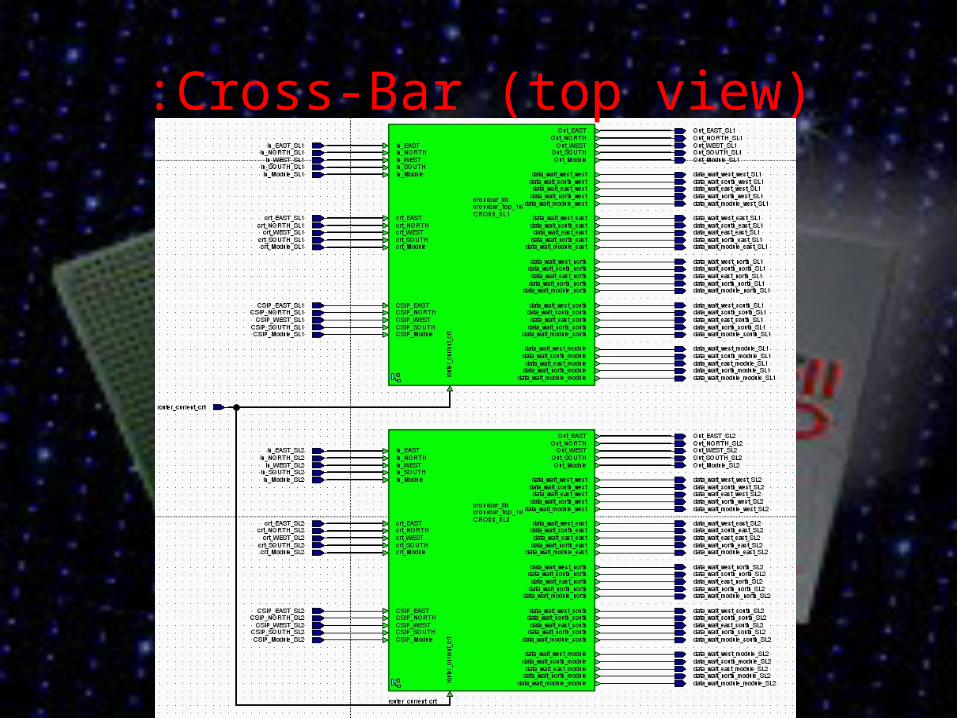
Cross-Bar (top view):

Cross-Bar:
Data from Input
CRT
direction
Data to output
CSIP
Data ready
(input for
Round Robin)
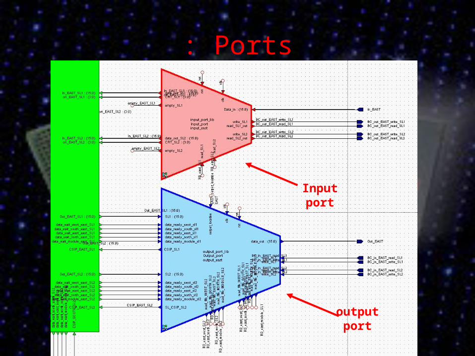
Ports:
output port
Input port

Input-Port (top-view)
Data in from
previous router/module
To crossbar

Input-Port:
Route to SL path
FIFO
+
CRT
read/write
control

Output-Port (top-view)
Data out to
next router/module
From crossbar

Output-Port (per SL):
NBS
Round Robin


Design Simulations:
1. Cross-Transmit
2. Buffer Credits
3. Round-Robin
4. Service-Level
5. Heavy Traffic

1 .Cross-Transmit:
3
cycles delay3 cycles delay
• Two Packets from different inputs to different outputs simultaneously

2 .Buffer Credits:
Filling NBS
Emptying NBS
1 cycle delay
• No transmission from output port if the next input port is full
• Output port controls the function

3 .Round-Robin:
Arbitraging between input port at the same SLIn a round form )round-robin(
Each flit is full packet
• When receiving flits from different inputs to the same output simultaneously, each flit is transmitted in turn

Not each flit is full packet
BODY EP
Arbitraging between input port at the same SLIn a round form )round-robin(
FP
3 .Round-Robin:
• Same as before, but with multi-flit packets

SL2 for 250 ns
(5 clock cycles)
1 cycle of SL1
2 cycle of SL2
1 cycle of SL1
3
cycles delay from input
)
3 cycle of SL2
4 .Service-Level: • Higher priority packet halts transmission of
a lower priority packet

5 .Heavy Traffic:
• receiving & transmitting simultaneously different SL, from and to different input & outputs
SL1 then SL2
SL2
SL2
SL1 then SL2
SL1
Round-Robin of SL2Round-Robin of SL1
Halt of SL2 for SL1

Simulation conclusions:
Latency = 3 clock cycles for a flit
Throughput = outputs 1 flit on each clock cycle(no wasted cycles)
No latency in output transition when between SLor in switching between inputs
Router can handle receiving & transmitting of multi-flit packets of different SL, from and to different inputs & outputs simultaneously

Second Semester Goals
Adding Virtual-Channel to Router architecture
Development of interface to the network
Final project goal : Implement a QNoC based application on
a FPGA for validation of NoC .

Project schedule - Achieving Final Goals
Implement Router On Virtex II Pro Validating & Extracting design parameters (area, timing) – 3 weeks
Add virtual channel to existing router – 3 weeks Ramp up understanding of PPC architecture or Micro-Blaze for connecting user-logic in order
to build a QNoC based application on the Virtex II Pro – 2 weeks
Design, implement & simulate interface – 4 weeks
Implement a QNoC based application ona FPGA for validation of NoC – 3 weeks