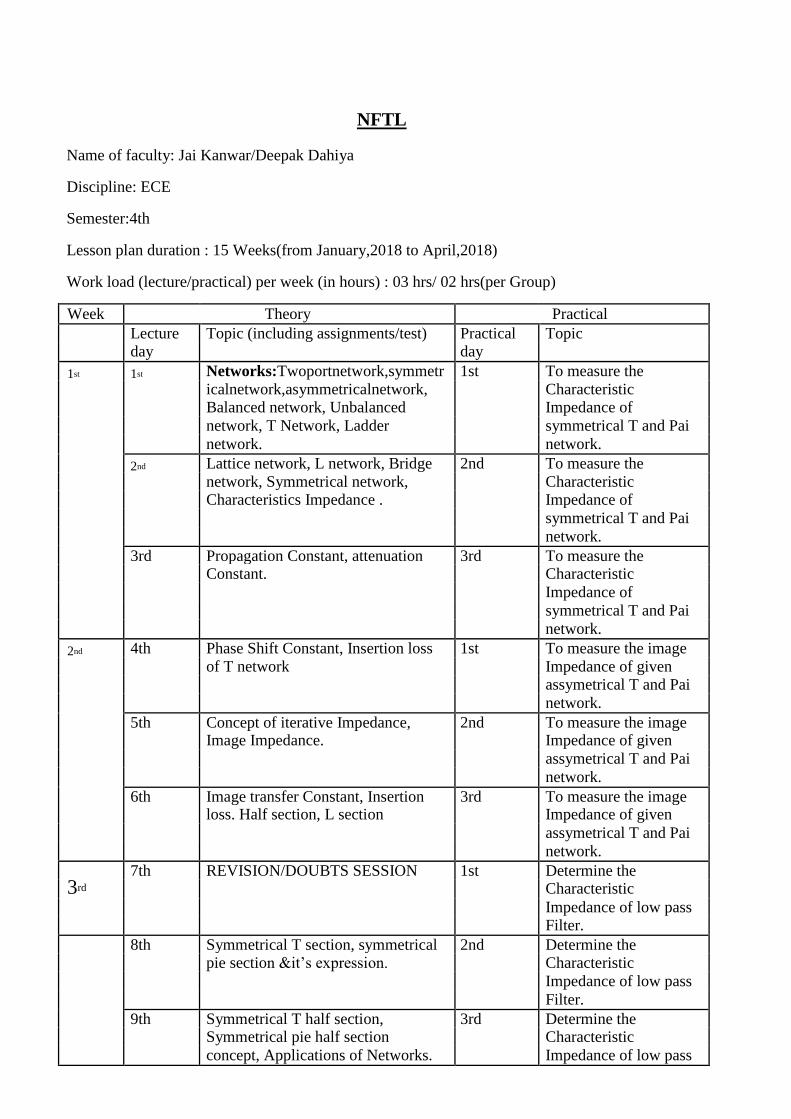
NFTL Name of faculty: Jai Kanwar/Deepak Dahiya
Discipline: ECE
Semester:4th
Lesson plan duration : 15 Weeks(from January,2018 to April,2018)
Work load (lecture/practical) per week (in hours) : 03 hrs/ 02 hrs(per Group)
Week Theory Practical
Lecture Topic (including assignments/test) Practical Topic day day
1st 1st Networks:Twoportnetwork,symmetr 1st To measure the icalnetwork,asymmetricalnetwork, Characteristic Balanced network, Unbalanced Impedance of
network, T Network, Ladder symmetrical T and Pai
network. network.
2nd Lattice network, L network, Bridge 2nd To measure the network, Symmetrical network, Characteristic Characteristics Impedance . Impedance of
symmetrical T and Pai
network.
3rd Propagation Constant, attenuation 3rd To measure the Constant. Characteristic
Impedance of
symmetrical T and Pai
network.
2nd 4th Phase Shift Constant, Insertion loss 1st To measure the image of T network Impedance of given assymetrical T and Pai
network.
5th Concept of iterative Impedance, 2nd To measure the image Image Impedance. Impedance of given
assymetrical T and Pai
network.
6th Image transfer Constant, Insertion 3rd To measure the image loss. Half section, L section Impedance of given
assymetrical T and Pai
network.
3rd
7th REVISION/DOUBTS SESSION 1st Determine the Characteristic
Impedance of low pass Filter.
8th Symmetrical T section, symmetrical 2nd Determine the pie section &it’s expression. Characteristic Impedance of low pass
Filter.
9th Symmetrical T half section, 3rd Determine the Symmetrical pie half section Characteristic
concept, Applications of Networks. Impedance of low pass
Filter.
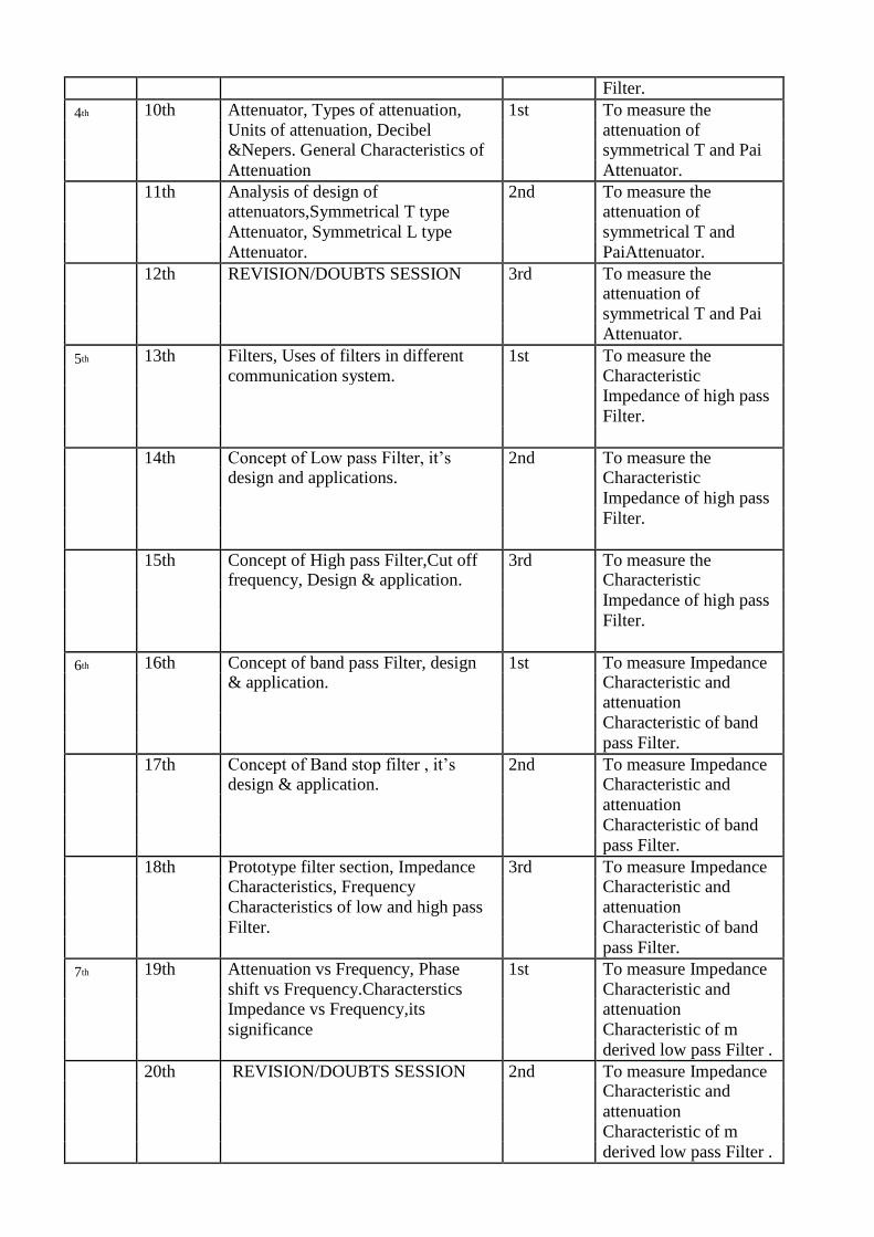
4th 10th Attenuator, Types of attenuation, 1st To measure the Units of attenuation, Decibel attenuation of &Nepers. General Characteristics of symmetrical T and Pai
Attenuation Attenuator.
11th Analysis of design of 2nd To measure the attenuators,Symmetrical T type attenuation of
Attenuator, Symmetrical L type symmetrical T and
Attenuator. PaiAttenuator.
12th REVISION/DOUBTS SESSION 3rd To measure the attenuation of
symmetrical T and Pai
Attenuator.
5th 13th Filters, Uses of filters in different 1st To measure the communication system. Characteristic Impedance of high pass
Filter.
14th Concept of Low pass Filter, it’s 2nd To measure the design and applications. Characteristic
Impedance of high pass
Filter.
15th Concept of High pass Filter,Cut off 3rd To measure the frequency, Design & application. Characteristic
Impedance of high pass
Filter.
6th 16th Concept of band pass Filter, design 1st To measure Impedance & application. Characteristic and attenuation
Characteristic of band
pass Filter.
17th Concept of Band stop filter , it’s 2nd To measure Impedance design & application. Characteristic and
attenuation
Characteristic of band
pass Filter.
18th Prototype filter section, Impedance 3rd To measure Impedance Characteristics, Frequency Characteristic and
Characteristics of low and high pass attenuation
Filter. Characteristic of band
pass Filter.
7th 19th Attenuation vs Frequency, Phase 1st To measure Impedance shift vs Frequency.Characterstics Characteristic and Impedance vs Frequency,its attenuation
significance Characteristic of m
derived low pass Filter .
20th REVISION/DOUBTS SESSION 2nd To measure Impedance Characteristic and
attenuation
Characteristic of m
derived low pass Filter .
21th Simple design of prototype low pass 3rd To measure Impedance
Filter and it’s application. Characteristic and
attenuation
Characteristic of m
derived low pass Filter .
8th 22th M derived Filter, limitations of 1st To observe the prototype filter , need of m derived information of standing Filter. wave on transmission
Line and measurement
of SWR.
23th Crystal Filter, crystal and it’s 2nd To observe the equivalent ckt, property of piezo information of standing
electric Filter and it’s uses wave on transmission
Line and measurement
of SWR.
24th Active Filters, basic concept of 3rd To observe the active filter, comparison of passive information of standing
Filter. wave on transmission
Line and measurement
of SWR.
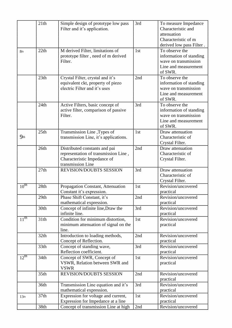
9th
25th Transmission Line ,Types of 1st Draw attenuation transmission Line, it’s applications. Characteristic of
Crystal Filter.
26th Distributed constants and pai 2nd Draw attenuation representation of transmission Line , Characteristic of
Characteristic Impedance of Crystal Filter.
transmission Line
27th REVISION/DOUBTS SESSION 3rd Draw attenuation Characteristic of
Crystal Filter.
10th 28th Propagation Constant, Attenuation 1st Revision/uncovered
Constant it’s expression. practical
29th Phase Shift Constant, it’s 2nd Revision/uncovered mathematical expression. practical
30th Concept of infinite line,Draw the 3rd Revision/uncovered infinite line. practical
11th 31th Condition for minimum distortion, 1st Revision/uncovered
minimum attenuation of signal on the practical line.
32th Introduction to loading methods, 2nd Revision/uncovered Concept of Reflection. practical
33th Concept of standing wave, 3rd Revision/uncovered Reflection coefficient. practical
12th 34th Concept of SWR, Concept of 1st Revision/uncovered
VSWR, Relation between SWR and practical VSWR
35th REVISION/DOUBTS SESSION 2nd Revision/uncovered practical
36th Transmission Line equation and it’s 3rd Revision/uncovered mathematical expression. practical
13th 37th Expression for voltage and current, 1st Revision/uncovered
Expression for Impedance at a line practical
38th Concept of transmission Line at high 2nd Revision/uncovered
frequency practical
39th REVISION/DOUBTS SESSION 3rd Revision/uncovered practical
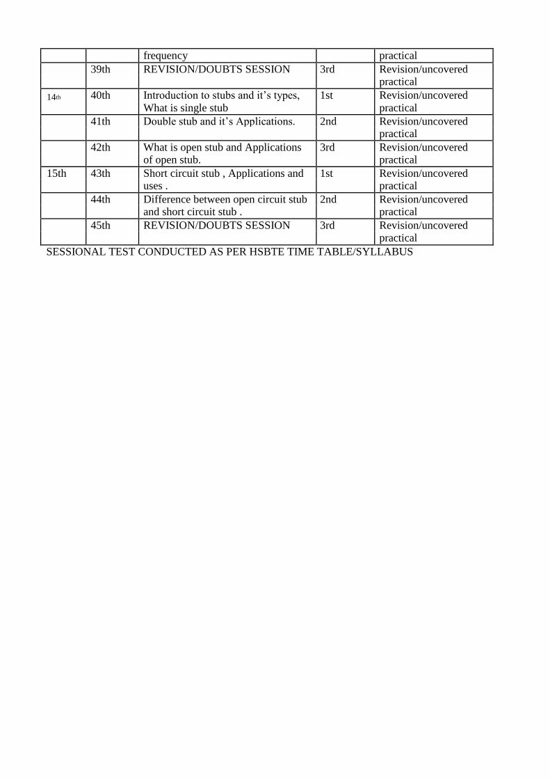
14th 40th Introduction to stubs and it’s types, 1st Revision/uncovered
What is single stub practical
41th Double stub and it’s Applications. 2nd Revision/uncovered practical
42th What is open stub and Applications 3rd Revision/uncovered of open stub. practical
15th 43th Short circuit stub , Applications and 1st Revision/uncovered uses . practical
44th Difference between open circuit stub 2nd Revision/uncovered and short circuit stub . practical
45th REVISION/DOUBTS SESSION 3rd Revision/uncovered practical
SESSIONAL TEST CONDUCTED AS PER HSBTE TIME TABLE/SYLLABUS
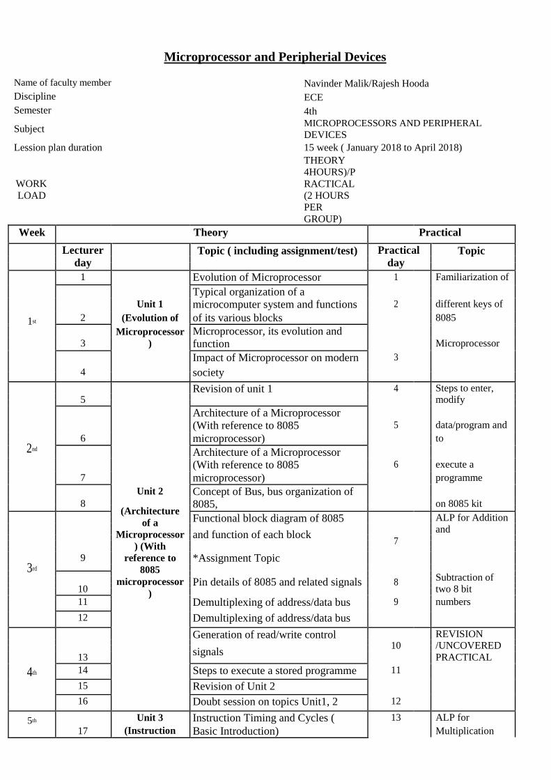
Microprocessor and Peripherial Devices
Name of faculty member Discipline Semester
Subject
Lession plan duration
WORK
LOAD
Navinder Malik/Rajesh Hooda ECE 4th MICROPROCESSORS AND PERIPHERAL
DEVICES 15 week ( January 2018 to April 2018) THEORY
4HOURS)/P
RACTICAL
(2 HOURS
PER GROUP)
Week Theory Practical
Lecturer Topic ( including assignment/test) Practical Topic
day
day
1 Evolution of Microprocessor 1 Familiarization of
Typical organization of a
Unit 1 microcomputer system and functions 2 different keys of
1st 2 (Evolution of of its various blocks 8085
Microprocessor, its evolution and
Microprocessor
3 ) function Microprocessor
Impact of Microprocessor on modern 3
4
society
Revision of unit 1 4 Steps to enter,
5
modify
Architecture of a Microprocessor
(With reference to 8085 5 data/program and
2nd
6 microprocessor) to
Architecture of a Microprocessor
(With reference to 8085 6 execute a
7 microprocessor) programme
Unit 2 Concept of Bus, bus organization of 8 8085, on 8085 kit
(Architecture
Functional block diagram of 8085
ALP for Addition of a
and Microprocessor and function of each block
7
) (With
3rd
9 reference to *Assignment Topic 8085
Subtraction of microprocessor Pin details of 8085 and related signals 8
10
two 8 bit )
11 Demultiplexing of address/data bus 9
numbers
12 Demultiplexing of address/data bus
Generation of read/write control REVISION
10
/UNCOVERED signals
13 PRACTICAL
4th
14 Steps to execute a stored programme 11
15 Revision of Unit 2
16 Doubt session on topics Unit1, 2 12
5th Unit 3 Instruction Timing and Cycles ( 13 ALP for
17 (Instruction Basic Introduction) Multiplication
Timing and and
Cycles)
14 division of two 8 Instruction cycle
18
bit
19 machine cycle 15 numbers
20 T-states
Fetch and execute cycle 16 ALP for
21
Arranging 10
Comparision between all the cyles 17 numbers in
6th 22
ascending /
23 Revision of Unit 3 18 descending order
Brief idea of machine and assembly
24 languages
Machines and Mnemonic codes 19 ALP for 0 to 9
25
BCD counters
Instruction format and Addressing 20
26
mode
7th
Identification of instructions as to 21
27
which addressing mode they belong
Identification of instructions as to
28 which addressing mode they belong
REVISION Concept of Instruction set 22 /UNCOVERED
29 PRACTICAL
Explanation of the instructions of the 23
th 30
following groups of instruction set
8 Unit
Explanation of the instructions of the
4(Programmin 24
31 following groups of instruction set
g with respect
to 8085 Explanation of the instructions of the
32 microprocessor following groups of instruction set
)
Data transfer group, Arithmetic 25 Interfacing
33
Group, Logic Group exercise on 8255
Stack, I/O and Machine Control 26 like LED display
34
Group control
9th
Programming exercises in assembly 27
35
language (with the help of examples)
Programming exercises in assembly
36 language (with the help of examples)
Revision of unit 4 28 Interfacing
37
exercise on
8253
10 th Doubt session on topics Unit 3,4 29 programmable
38
interval
39 Concept of memory mapping, 30
40 partitioning of total memory space timer
REVISION Unit 5 Address decoding 31 /UNCOVERED
11th 41 PRACTICAL
(Memories and concept of peripheral mapped I/O and
I/O interfacing)
memory mapped I/O 32
42 * Assignment Topic
concept of peripheral mapped I/O and 33
43
memory mapped I/O
Interfacing of memory mapped I/O
44 devices
Interfacing of memory mapped I/O 34 Interfacing
45
devices exercise on 8279
Revision of unit 5 35 programmable
46
KB/display
12th Concept of interrupt, Maskable and 36
47
non-maskable interface
Edge triggered and level triggered
interrupts, Software interrupt, Restart
48 interrupts and its use
Various hardware interrupts of 8085 37 Use of 8085
49
emulator for
Servicing interrupts, extending 38
50 Unit 6 interrupt system hardware testing 13th
Concept of programmed I/O
(Interrupts) 39
51
operations,
sync data transfer, async data transfer
52 (hand shaking)
Interrupt driven data transfer, DMA REVISION 40 /UNCOVERED
th 53 Unit 7 (Data and * Assignment Topic PRACTICAL
14 54 Serial output data, Serial input data 41
Transfer
55 Revision of unit 6,7 42
Techniques)
56 8255 PPI and 8253 PIT
57 8257 / 8237 DMA controller
8279 Programmable KB/Display REVISION Unit 8 43 /UNCOVERED
15th 58 Interface PRACTICAL
(Peripheral
8251 Communication Interface 44
59 devices) Adapter
60 Revision of unit 8 45
Test conducted as per Annual
Calendar
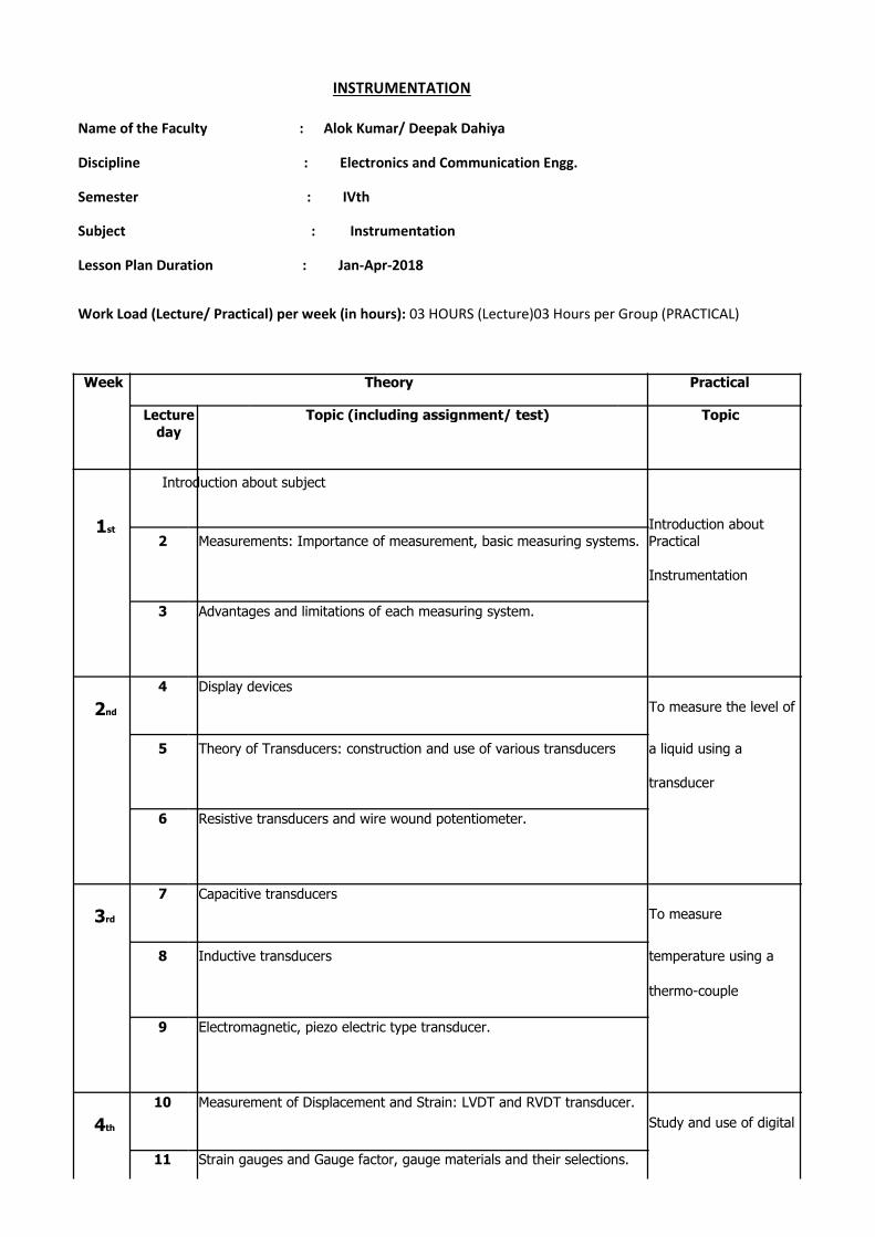
INSTRUMENTATION
Name of the Faculty : Alok Kumar/ Deepak Dahiya
Discipline : Electronics and Communication Engg.
Semester : IVth
Subject : Instrumentation
Lesson Plan Duration : Jan-Apr-2018
Work Load (Lecture/ Practical) per week (in hours): 03 HOURS (Lecture)03 Hours per Group (PRACTICAL)
Week Theory Practical
Lecture Topic (including assignment/ test) Topic
day
Introduction about subject
1st Introduction about
2 Measurements: Importance of measurement, basic measuring systems. Practical
Instrumentation
3 Advantages and limitations of each measuring system.
4 Display devices
2nd To measure the level of
5 Theory of Transducers: construction and use of various transducers a liquid using a
transducer
6 Resistive transducers and wire wound potentiometer.
7 Capacitive transducers
3rd To measure
8 Inductive transducers temperature using a
thermo-couple
9 Electromagnetic, piezo electric type transducer.
10 Measurement of Displacement and Strain: LVDT and RVDT transducer.
4th Study and use of digital
11 Strain gauges and Gauge factor, gauge materials and their selections.
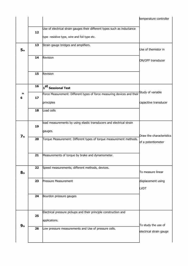
temperature controller
Use of electrical strain gauges their different types such as inductance
12
type resistive type, wire and foil type etc.
13 Strain gauge bridges and amplifiers.
5th Use of themistor in
14 Revision ON/OFF transducer
15 Revision
16 1st
Sessional Test
Study of variable th Force Measurement: Different types of force measuring devices and their
6 17
principles capacitive transducer
18 Load cells
load measurements by using elastic transducers and electrical strain
19
gauges.
7th Draw the characteristics
20 Torque Measurement: Different types of torque measurement methods. of a potentiometer
21 Measurements of torque by brake and dynamometer.
22 Speed measurements; different methods, devices.
8th To measure linear
23 Pressure Measurement displacement using
LVDT
24 Bourdon pressure gauges
Electrical pressure pickups and their principle construction and
25
applications.
9th To study the use of
26 Low pressure measurements and Use of pressure cells. electrical strain gauge
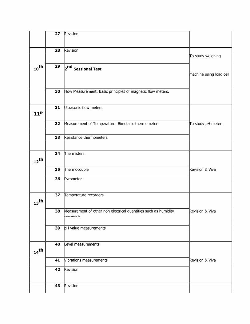
27 Revision
28 Revision
To study weighing
10th 29
2nd
Sessional Test
machine using load cell
30 Flow Measurement: Basic principles of magnetic flow meters.
31 Ultrasonic flow meters
11th
32 Measurement of Temperature: Bimetallic thermometer. To study pH meter.
33 Resistance thermometers
34 Thermisters
12th
35 Thermocouple Revision & Viva
36 Pyrometer
37 Temperature recorders
13th
38 Measurement of other non electrical quantities such as humidity Revision & Viva
measurements.
39 pH value measurements
40 Level measurements
14th
41 Vibrations measurements Revision & Viva
42 Revision
43 Revision
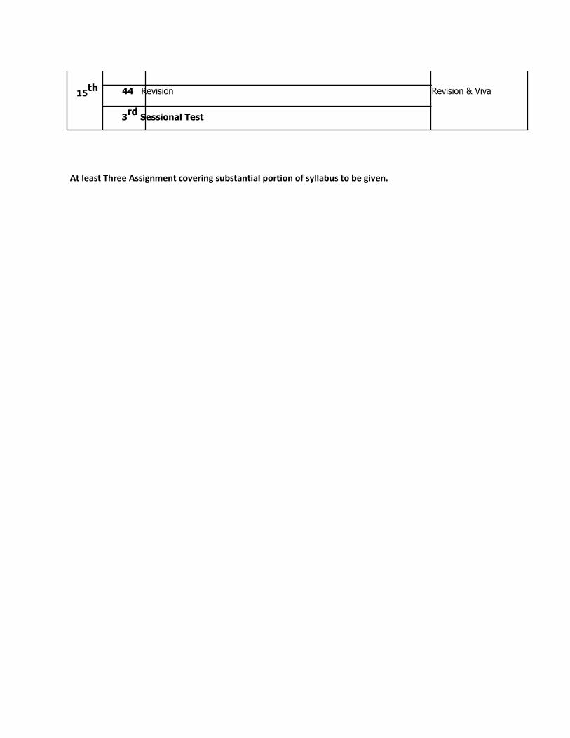
15th
44 Revision Revision & Viva
3rd
Sessional Test
At least Three Assignment covering substantial portion of syllabus to be given.
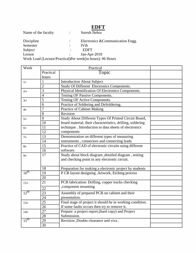
EDFT
Name of the faculty : Suresh Nehra
Discipline : Electronics &Communication Engg.
Semester : IVth
Subject : EDFT
Lesson : Jan-Apr-2018
Work Load (Lecture/Practical)Per week(in hours): 06 Hours
Week Practical
Practical Topic hours
1st 1 Introduction About Subject
2 Study Of Different Electronics Components.
2nd 3 Physical Identification Of Electronics Components.
4 Testing OF Passive Components.
3rd 5 Testing OF Active Components.
6 Practice of Soldering and DeSoldering.
4th 7 Practice of Cabinet Making
8 Revision
5th 9 Study About Different Types Of Printed Circuit Board,
10 board material, their characteristics, drilling, soldering
6th 11 technique . Introduction to data sheets of electronics
12 components
7th 13 Demonstration on different types of measuring
14 instruments , connectors and connecting leads
8th 15 Practice of CAD of electronic circuits using different
16 software.
9th 17 Study about block diagram ,detailed diagram , testing
and checking point in any electronic circuit.
18 Preparation for making a electronic project by students
10th 19 P CB layout designing ,Artwork, Etching process
20
11th 21 PCB fabrication: Drilling, copper tracks checking
,component mounting
22
12th 23 Assembly of prepared PCB on cabinet and their
24 presentation.
13th 25 Final stage of project it should be in working condition.
26 If some faults occurs then try to remove it.
14th 27 Prepare a project report.(hard copy) and Project
28 Submission.
15th 29 Revision ,Doubts clearance and viva .
30
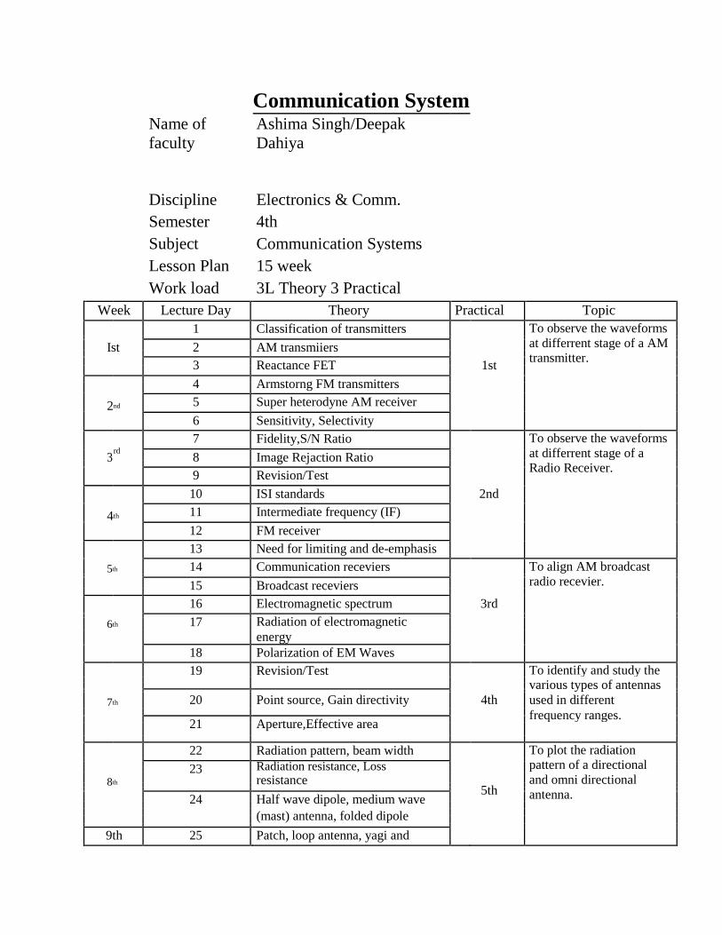
Communication System
Name of
faculty
Ashima Singh/Deepak
Dahiya
Discipline Electronics & Comm.
Semester 4th
Subject Communication Systems
Lesson Plan 15 week
Work load 3L Theory 3 Practical
Week Lecture Day Theory Practical Topic
1 Classification of transmitters To observe the waveforms
at differrent stage of a AM Ist 2 AM transmiiers
transmitter. 3
Reactance FET
1st
4
Armstorng FM transmitters
2nd 5 Super heterodyne AM receiver
6 Sensitivity, Selectivity
7 Fidelity,S/N Ratio To observe the waveforms
rd
at differrent stage of a 3 8 Image Rejaction Ratio
Radio Receiver. 9
Revision/Test
10 ISI standards 2nd
4th 11 Intermediate frequency (IF)
12 FM receiver
13 Need for limiting and de-emphasis
5th 14 Communication receviers To align AM broadcast
radio recevier. 15 Broadcast receviers
16 Electromagnetic spectrum 3rd
6th 17
Radiation of electromagnetic
energy
18 Polarization of EM Waves 19 Revision/Test To identify and study the
various types of antennas
7th 20 Point source, Gain directivity 4th used in different
frequency ranges.
21
Aperture,Effective area
22 Radiation pattern, beam width To plot the radiation
pattern of a directional 23 Radiation resistance, Loss
8th resistance and omni directional
5th
antenna. 24 Half wave dipole, medium wave
(mast) antenna, folded dipole
9th 25 Patch, loop antenna, yagi and
ferrite rod antenna
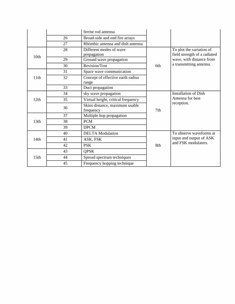
26 Broad-side and end fire arrays
27 Rhombic antenna and dish antenna
28 Different modes of wave To plot the variation of
propagation
field strength of a radiated 10th
29 Ground wave propagation wave, with distance from
a transmitting antenna. 30 Revision/Test 6th
31 Space wave communication
11th 32 Concept of effective earth radius
range
33 Duct propagation
34 sky wave propagation Installation of Dish
Antenna for best 12th 35 Virtual height, critical frequency
reception.
Skins distance, maximum usable
36
frequency 7th
37 Multiple hop propagation
13th 38 PCM
39 DPCM
40 DELTA Modulation To observe waveforms at
input and output of ASK 14th 41 ASK, FSK
and FSK modulaters. 42 PSK 8th
43 QPSK
15th 44 Spread spectrum techniques
45 Frequency hopping technique
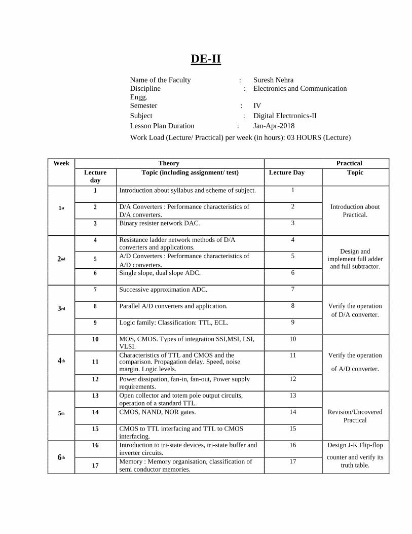
DE-II
Name of the Faculty : Suresh Nehra
Discipline : Electronics and Communication
Engg.
Semester : IV
Subject : Digital Electronics-II
Lesson Plan Duration : Jan-Apr-2018
Work Load (Lecture/ Practical) per week (in hours): 03 HOURS (Lecture)
Week Theory Practical
Lecture Topic (including assignment/ test) Lecture Day Topic
day
1 Introduction about syllabus and scheme of subject. 1
1st 2 D/A Converters : Performance characteristics of 2 Introduction about
D/A converters. Practical.
3 Binary resister network DAC. 3
4 Resistance ladder network methods of D/A 4
converters and applications.
Design and
2nd
A/D Converters : Performance characteristics of 5
5 implement full adder
A/D converters. and full subtractor.
6 Single slope, dual slope ADC. 6
7 Successive approximation ADC. 7
3rd 8 Parallel A/D converters and application. 8 Verify the operation
of D/A converter. 9 Logic family: Classification: TTL, ECL. 9
10 MOS, CMOS. Types of integration SSI,MSI, LSI, 10
VLSI.
4th
Characteristics of TTL and CMOS and the 11 Verify the operation 11 comparison. Propagation delay. Speed, noise
margin. Logic levels. of A/D converter.
12 Power dissipation, fan-in, fan-out, Power supply 12
requirements.
13 Open collector and totem pole output circuits, 13
operation of a standard TTL.
5th 14 CMOS, NAND, NOR gates. 14 Revision/Uncovered
Practical
15 CMOS to TTL interfacing and TTL to CMOS 15
interfacing.
16 Introduction to tri-state devices, tri-state buffer and 16 Design J-K Flip-flop
6th inverter circuits.
counter and verify its
Memory : Memory organisation, classification of 17 17 truth table.
semi conductor memories.
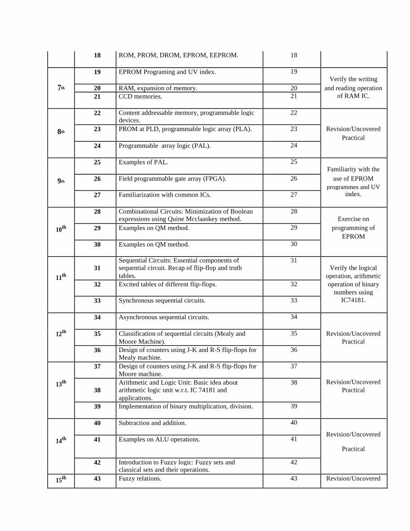
18 ROM, PROM, DROM, EPROM, EEPROM. 18
19 EPROM Programing and UV index. 19 Verify the writing
7th
20 RAM, expansion of memory. 20 and reading operation
21 CCD memories. 21 of RAM IC.
22 Content addressable memory, programmable logic 22
devices.
8th 23 PROM at PLD, programmable logic array (PLA). 23 Revision/Uncovered
Practical 24 Programmable array logic (PAL). 24
25 Examples of PAL. 25 Familiarity with the
9th 26 Field programmable gate array (FPGA). 26 use of EPROM
programmes and UV
27 Familiarization with common ICs. 27 index.
28 Combinational Circuits: Minimization of Boolean 28
expressions using Quine Mcclaaskey method.
Exercise on
10th 29 Examples on QM method. 29 programming of
EPROM 30 Examples on QM method. 30
Sequential Circuits: Essential components of 31
31 sequential circuit. Recap of flip-flop and truth Verify the logical
11th tables. operation, arithmetic
32 Excited tables of different flip-flops. 32 operation of binary
numbers using
33 Synchronous sequential circuits. 33 IC74181.
34 Asynchronous sequential circuits. 34
12th 35 Classification of sequential circuits (Mealy and 35 Revision/Uncovered
Moore Machine). Practical
36 Design of counters using J-K and R-S flip-flops for 36
Mealy machine.
37 Design of counters using J-K and R-S flip-flops for 37
Moore machine.
13th Arithmetic and Logic Unit: Basic idea about 38 Revision/Uncovered
38 arithmetic logic unit w.r.t. IC 74181 and Practical
applications.
39 Implementation of binary multiplication, division. 39
40 Subtraction and addition. 40
Revision/Uncovered 14
th 41 Examples on ALU operations. 41
Practical
42 Introduction to Fuzzy logic: Fuzzy sets and 42
classical sets and their operations.
15th 43 Fuzzy relations. 43 Revision/Uncovered
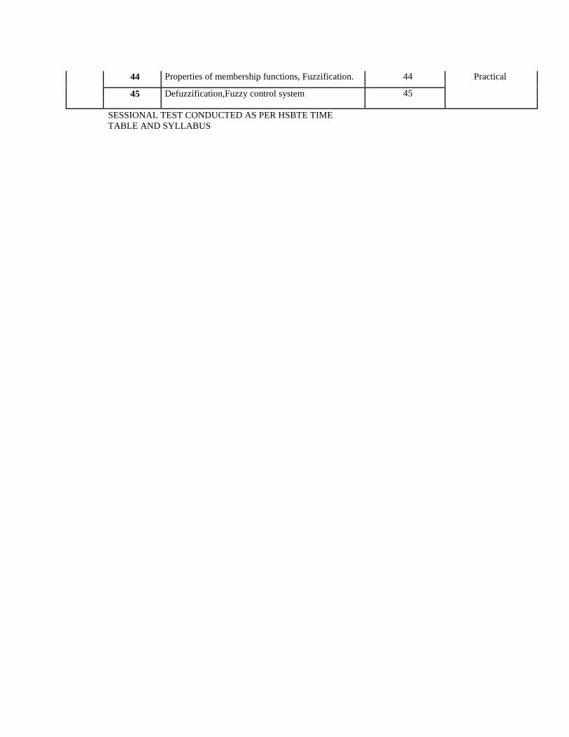
44 Properties of membership functions, Fuzzification. 44 Practical
45 Defuzzification,Fuzzy control system 45
SESSIONAL TEST CONDUCTED AS PER HSBTE TIME
TABLE AND SYLLABUS
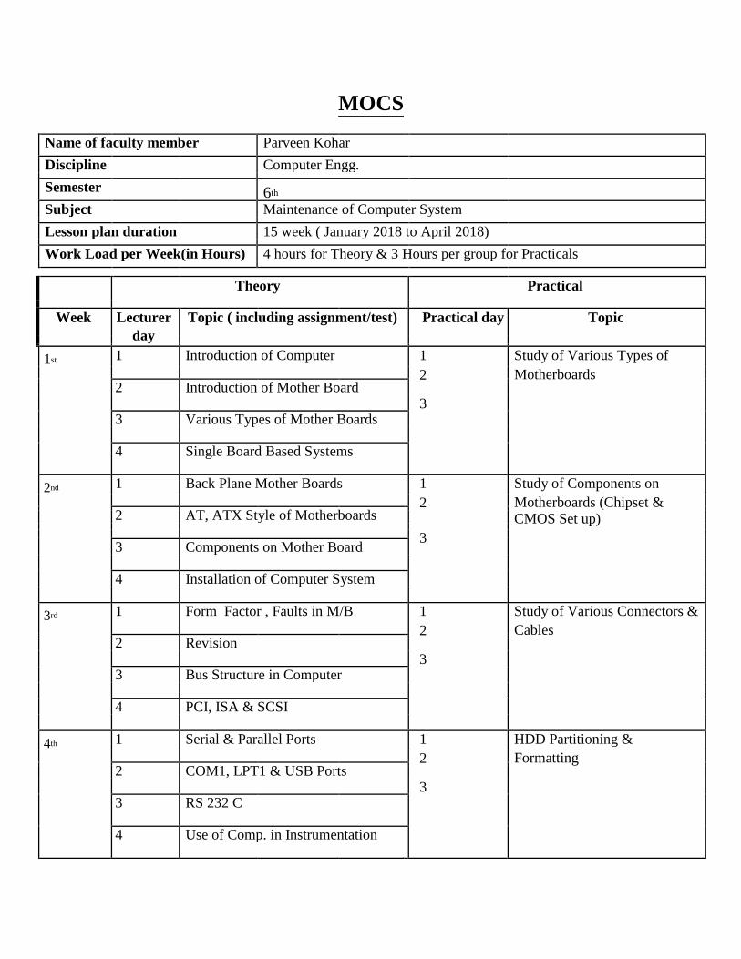
MOCS
Name of faculty member Parveen Kohar
Discipline Computer Engg.
Semester 6th
Subject Maintenance of Computer System
Lesson plan duration 15 week ( January 2018 to April 2018)
Work Load per Week(in Hours) 4 hours for Theory & 3 Hours per group for Practicals
Theory Practical
Week Lecturer Topic ( including assignment/test) Practical day Topic
day
1st 1 Introduction of Computer 1 Study of Various Types of 2 Motherboards
2 Introduction of Mother Board
3
3 Various Types of Mother Boards
4 Single Board Based Systems
2nd 1 Back Plane Mother Boards 1 Study of Components on 2 Motherboards (Chipset &
2 AT, ATX Style of Motherboards CMOS Set up)
3
3 Components on Mother Board
4 Installation of Computer System
3rd 1 Form Factor , Faults in M/B 1 Study of Various Connectors & 2 Cables
2 Revision
3
3 Bus Structure in Computer
4 PCI, ISA & SCSI
4th 1 Serial & Parallel Ports 1 HDD Partitioning & 2 Formatting
2 COM1, LPT1 & USB Ports
3
3 RS 232 C
4 Use of Comp. in Instrumentation
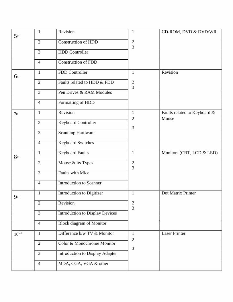
5th
1 Revision 1 CD-ROM, DVD & DVD/WR
2 Construction of HDD 2 3
3 HDD Controller
4 Construction of FDD
6th
1 FDD Controller 1 Revision
2 Faults related to HDD & FDD 2 3
3 Pen Drives & RAM Modules
4 Formatting of HDD
7th 1 Revision 1 Faults related to Keyboard & 2 Mouse
2 Keyboard Controller
3
3 Scanning Hardware
4 Keyboard Switches
8th
1 Keyboard Faults 1 Monitors (CRT, LCD & LED)
2 Mouse & its Types 2 3
3 Faults with Mice
4 Introduction to Scanner
9th
1 Introduction to Digitizer 1 Dot Matrix Printer
2 Revision 2 3
3 Introduction to Display Devices
4 Block diagram of Monitor
10th 1 Difference b/w TV & Monitor 1 Laser Printer
2
2 Color & Monochrome Monitor 3
3 Introduction to Display Adapter
4 MDA, CGA, VGA & other
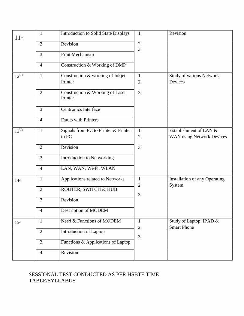
11th
1 Introduction to Solid State Displays 1 Revision
2 Revision 2 3
3 Print Mechanism
4 Construction & Working of DMP
12th 1 Construction & working of Inkjet 1 Study of various Network
Printer 2 Devices
2 Construction & Working of Laser 3 Printer
3 Centronics Interface
4 Faults with Printers
13th 1 Signals from PC to Printer & Printer 1 Establishment of LAN &
to PC 2 WAN using Network Devices
2 Revision 3
3 Introduction to Networking
4 LAN, WAN, Wi-Fi, WLAN
14th 1 Applications related to Networks 1 Installation of any Operating 2 System
2 ROUTER, SWITCH & HUB
3
3 Revision
4 Description of MODEM
15th 1 Need & Functions of MODEM 1 Study of Laptop, IPAD & 2 Smart Phone
2 Introduction of Laptop
3
3 Functions & Applications of Laptop
4 Revision
SESSIONAL TEST CONDUCTED AS PER HSBTE TIME
TABLE/SYLLABUS
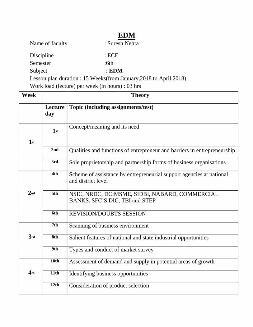
EDM
Name of faculty : Suresh Nehra
Discipline : ECE
Semester :6th
Subject : EDM
Lesson plan duration : 15 Weeks(from January,2018 to April,2018)
Work load (lecture) per week (in hours) : 03 hrs
Week Theory
Lecture Topic (including assignments/test) day
1st
Concept/meaning and its need
1st
2nd Qualities and functions of entrepreneur and barriers in entrepreneurship
3rd Sole proprietorship and partnership forms of business organisations
4th Scheme of assistance by entrepreneurial support agencies at national and district level
2nd
5th NSIC, NRDC, DC:MSME, SIDBI, NABARD, COMMERCIAL BANKS, SFC’S DIC, TBI and STEP
6th REVISION/DOUBTS SESSION
7th Scanning of business environment
3rd
8th Salient features of national and state industrial opportunities
9th Types and conduct of market survey
10th Assessment of demand and supply in potential areas of growth
4th
11th Identifying business opportunities
12th Consideration of product selection
13th REVISION/DOUBTS SESSION
5th
14th REVISION/Test
15th Visit from market survey
16th Visit from market survey
6th
17th Preliminary project report
18th Detailed project report including technical, economic and market feasibility
19th Common errors in project report preparation
7th
20th Exercises on preparation of project report
21th Project reports collection from internet for different products
22th Definition and importance of management
8th
23th Functions of management: Importance of planning, organising, staffing, directing and controlling
24th Principles of management, concept and structure of an organisation
25th Line organisation, line and staff organisation, functional organisation
9th
26th REVISION/Test
27th Definition and need of leadership, qualities and function of a leader
28th Manager Vs leader, types of leadership
10th
29th Definition, characterstic of motivation
30th Factors affecting motivation, theories of motivation
31th Introduction and objective of human resource management, manpower 11 th planning, recruitment and selection
32th Introduction to performance appraisal method
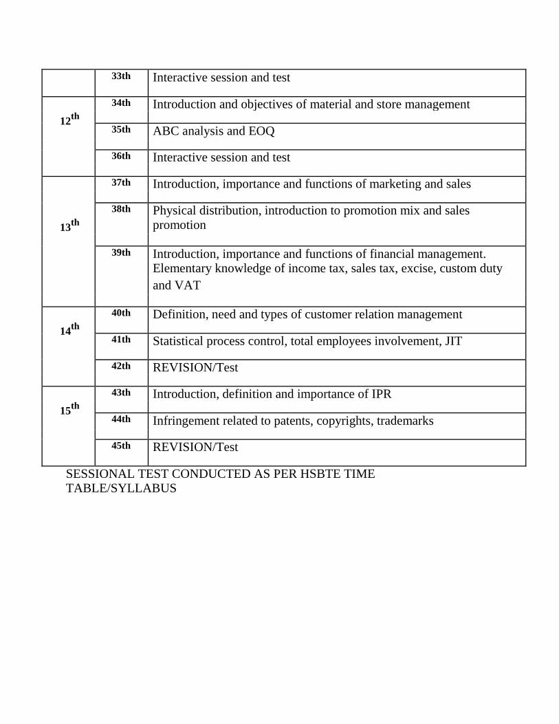
33th Interactive session and test
34th Introduction and objectives of material and store management
12th
35th ABC analysis and EOQ
36th Interactive session and test
37th Introduction, importance and functions of marketing and sales
38th Physical distribution, introduction to promotion mix and sales
13th promotion
39th Introduction, importance and functions of financial management. Elementary knowledge of income tax, sales tax, excise, custom duty
and VAT
40th Definition, need and types of customer relation management
14th
41th Statistical process control, total employees involvement, JIT
42th REVISION/Test
43th Introduction, definition and importance of IPR
15th
44th Infringement related to patents, copyrights, trademarks
45th REVISION/Test
SESSIONAL TEST CONDUCTED AS PER HSBTE TIME TABLE/SYLLABUS
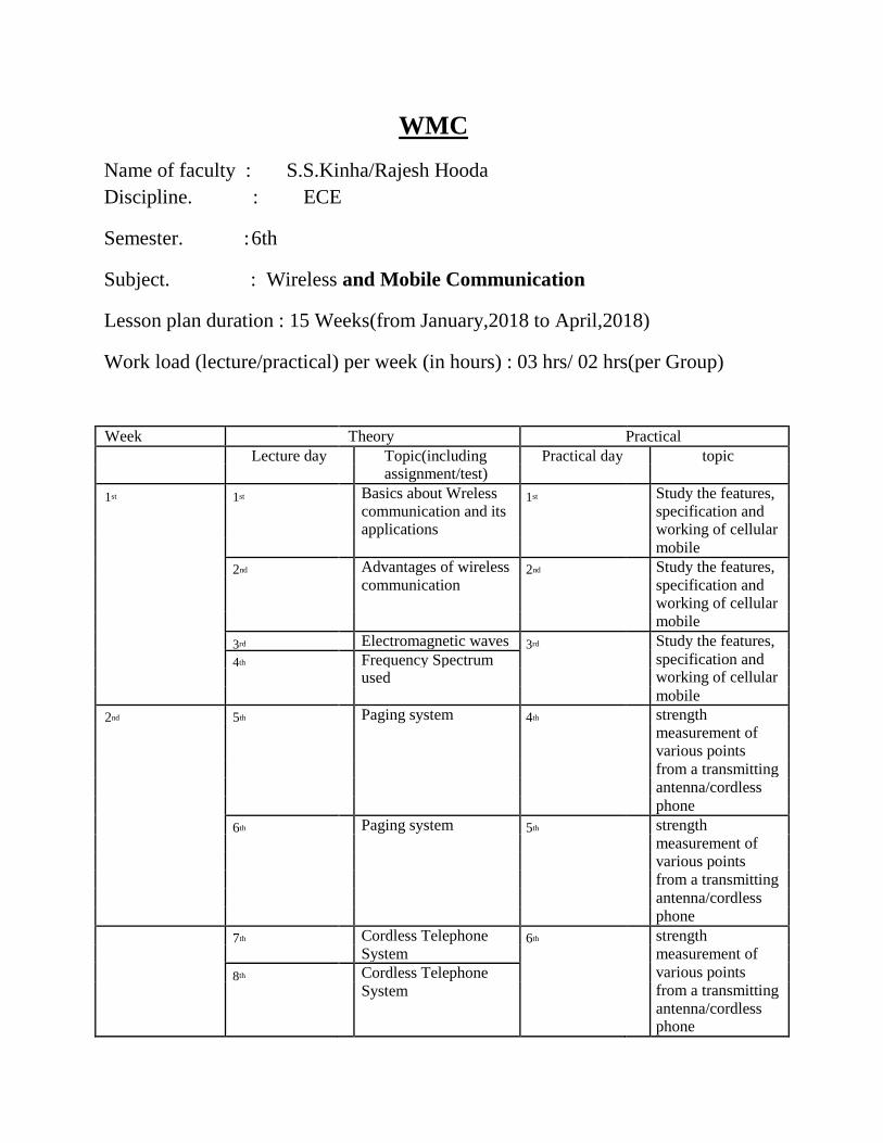
WMC
Name of faculty : S.S.Kinha/Rajesh Hooda
Discipline. : ECE
Semester. : 6th
Subject. : Wireless and Mobile Communication
Lesson plan duration : 15 Weeks(from January,2018 to April,2018)
Work load (lecture/practical) per week (in hours) : 03 hrs/ 02 hrs(per Group)
Week Theory Practical
Lecture day Topic(including Practical day topic assignment/test)
1st 1st Basics about Wreless 1st Study the features, communication and its specification and applications working of cellular
mobile
2nd Advantages of wireless 2nd Study the features, communication specification and working of cellular
mobile
3rd Electromagnetic waves 3rd Study the features,
4th Frequency Spectrum specification and used working of cellular mobile
2nd 5th Paging system 4th strength measurement of various points from a transmitting
antenna/cordless
phone
6th Paging system 5th strength measurement of various points from a transmitting antenna/cordless
phone
7th Cordless Telephone 6th strength System measurement of
8th Cordless Telephone various points System from a transmitting antenna/cordless phone
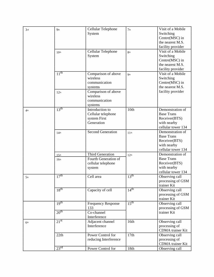
3rd 9th Cellular Telephone 7th Visit of a Mobile System Switching Centre(MSC) in
the nearest M.S.
facility provider
10th Cellular Telephone 8th Visit of a Mobile System Switching Centre(MSC) in the nearest M.S.
facility provider
11th Comparison of above 9th Visit of a Mobile wireless Switching communication Centre(MSC) in systems the nearest M.S.
12th Comparison of above facility provider wireless
communication
systems
4th 13th Introduction to 10th Demonstration of Cellular telephone Base Trans system First Receiver(BTS)
Generation with nearby
cellular tower 134
14th Second Generation 11th Demonstration of Base Trans Receiver(BTS) with nearby
cellular tower 134
15th Third Generation 12th Demonstration of
16th Fourth Generation of Base Trans cellular telephone Receiver(BTS) system with nearby
cellular tower 134
5th 17th Cell area 13th Observing call processing of GSM trainer Kit
18th Capacity of cell 14th Observing call processing of GSM trainer Kit
19th Frequency Response 15th Observing call 133 processing of GSM
20th Co-channel trainer Kit
Interference
6th 21st Adjacent channel 16th Observing call Interference processing of CDMA trainer Kit
22th Power Control for 17th Observing call reducing Interference processing of
CDMA trainer Kit
23rd Power Control for 18th Observing call
reducing Interference processing of
24th Improving coverage CDMA trainer Kit and capacity in cellular
system a) Cell
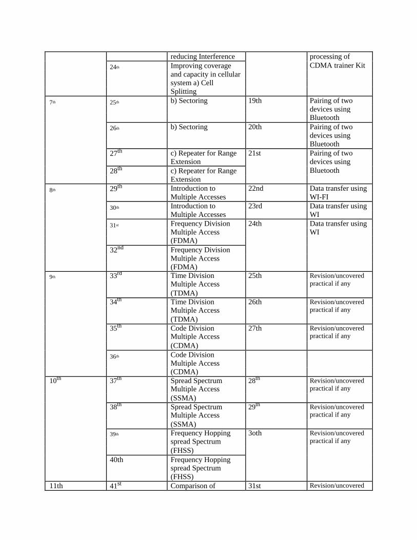
Splitting
7th 25th b) Sectoring 19th Pairing of two devices using Bluetooth
26th b) Sectoring 20th Pairing of two devices using Bluetooth
27th c) Repeater for Range 21st Pairing of two Extension devices using
28th c) Repeater for Range Bluetooth
Extension
8th 29th Introduction to 22nd Data transfer using Multiple Accesses WI-FI
30th Introduction to 23rd Data transfer using Multiple Accesses WI
31st Frequency Division 24th Data transfer using Multiple Access WI (FDMA)
32nd Frequency Division
Multiple Access
(FDMA)
9th 33rd Time Division 25th Revision/uncovered
Multiple Access practical if any
(TDMA) 34th Time Division 26th Revision/uncovered
Multiple Access practical if any
(TDMA)
35th Code Division 27th Revision/uncovered
Multiple Access practical if any
(CDMA)
36th Code Division
Multiple Access
(CDMA)
10th 37th Spread Spectrum 28th Revision/uncovered
Multiple Access practical if any
(SSMA)
38th Spread Spectrum 29th Revision/uncovered
Multiple Access practical if any
(SSMA) 39th Frequency Hopping 3oth Revision/uncovered
spread Spectrum practical if any
(FHSS)
40th Frequency Hopping
spread Spectrum
(FHSS)
11th 41st Comparison of 31st Revision/uncovered
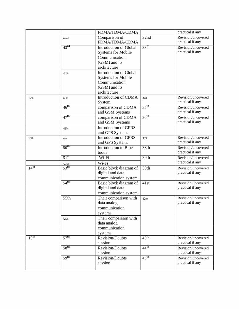
FDMA/TDMA/CDMA practical if any
42nd Comparison of 32nd Revision/uncovered
FDMA/TDMA/CDMA practical if any
43rd Introduction of Global 33rd Revision/uncovered
Systems for Mobile practical if any
Communication
(GSM) and its
architecture
44th Introduction of Global
Systems for Mobile
Communication
(GSM) and its
architecture
12th 45th Introduction of CDMA 34th Revision/uncovered
System practical if any
46th comparison of CDMA 35th Revision/uncovered
and GSM Systems practical if any
47th comparison of CDMA 36th Revision/uncovered
and GSM Systems practical if any
48th Introduction of GPRS
and GPS System.
13th 49th Introduction of GPRS 37th Revision/uncovered
and GPS System. practical if any
50th Introduction to Blue 38th Revision/uncovered
tooth practical if any
51st Wi-Fi 39th Revision/uncovered
practical if any 52nd Wi-Fi
14th 53rd Basic block diagram of 30th Revision/uncovered
digital and data practical if any
communication system
54th Basic block diagram of 41st Revision/uncovered
digital and data practical if any
communication system
55th Their comparison with 42nd Revision/uncovered
data analog practical if any
communication
systems
56th Their comparison with
data analog
communication
systems
15th 57th Revision/Doubts 43rd Revision/uncovered
session practical if any
58th Revision/Doubts 44th Revision/uncovered
session practical if any
59th Revision/Doubts 45th Revision/uncovered
session practical if any

Medical Electronics
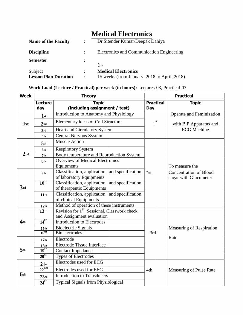
Name of the Faculty : Dr.Sitender Kumar/Deepak Dahiya
Discipline : Electronics and Communication Engineering
Semester : 6th
Subject : Medical Electronics
Lesson Plan Duration : 15 weeks (from January, 2018 to April, 2018)
Work Load (Lecture / Practical) per week (in hours): Lectures-03, Practical-03
Week Theory Practical
Lecture Topic Practical Topic
day (including assignment / test) Day
1st Introduction to Anatomy and Physiology Operate and Feminization
2nd Elementary ideas of Cell Structure
st 1st 1 with B.P Apparatus and
3rd Heart and Circulatory System ECG Machine
4th Central Nervous System
5th Muscle Action
2nd
6th Respiratory System
7th Body temperature and Reproduction System
8th Overview of Medical Electronics Equipments To measure the
Classification, application and specification 2nd
9th Concentration of Blood of laboratory Equipments sugar with Glucometer
3rd
10 th Classification, application and specification
of therapeutic Equipments
11th Classification, application and specification of clinical Equipments
12th Method of operation of these instruments
13 th Revision for 1st
Sessional, Classwork check
and Assignment evaluation
4th
14th
Introduction to Electrodes
15th Bioelectric Signals Measuring of Respiration 16th Bio electrodes 3rd
Rate 17th Electrode
5th
18th Electrode Tissue Interface
19th Contact Impedance
20th
Types of Electrodes
21st Electrodes used for ECG
6th
22nd Electrodes used for EEG 4th Measuring of Pulse Rate
23rd Introduction to Transducers
24th Typical Signals from Physiological
Week Theory Practical
Lecture Topic Practical Topic
day (including assignment / test) Day
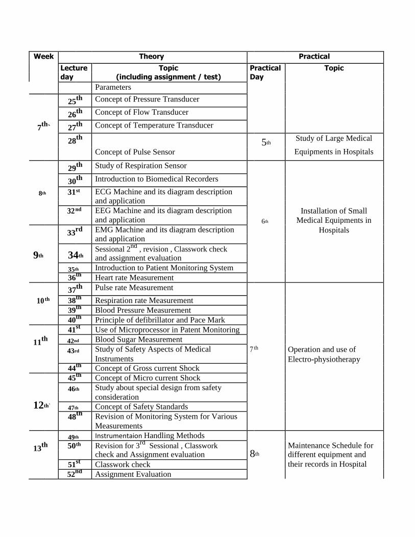
Parameters
25th Concept of Pressure Transducer
26th Concept of Flow Transducer
7th
` 27th Concept of Temperature Transducer
28th
5th Study of Large Medical
Concept of Pulse Sensor Equipments in Hospitals
29th Study of Respiration Sensor
30th Introduction to Biomedical Recorders
8th 31 st ECG Machine and its diagram description
and application
32 nd EEG Machine and its diagram description Installation of Small
and application
6th Medical Equipments in
33rd EMG Machine and its diagram description Hospitals
and application
9th
34th
Sessional 2nd
, revision , Classwork check and assignment evaluation
35th Introduction to Patient Monitoring System
36th Heart rate Measurement
37th Pulse rate Measurement
10 th 38th Respiration rate Measurement
39th Blood Pressure Measurement
40th Principle of defibrillator and Pace Mark
41st Use of Microprocessor in Patent Monitoring
11th 42nd Blood Sugar Measurement
43rd Study of Safety Aspects of Medical 7 th Operation and use of Instruments Electro-physiotherapy
44th Concept of Gross current Shock
45th Concept of Micro current Shock
46th Study about special design from safety
12th`
consideration
47th Concept of Safety Standards
48th Revision of Monitoring System for Various
Measurements
49th Instrumentaion Handling Methods
13th 50 th Revision for 3
rd Sessional , Classwork
8th
Maintenance Schedule for check and Assignment evaluation different equipment and
51st Classwork check their records in Hospital
52nd Assignment Evaluation
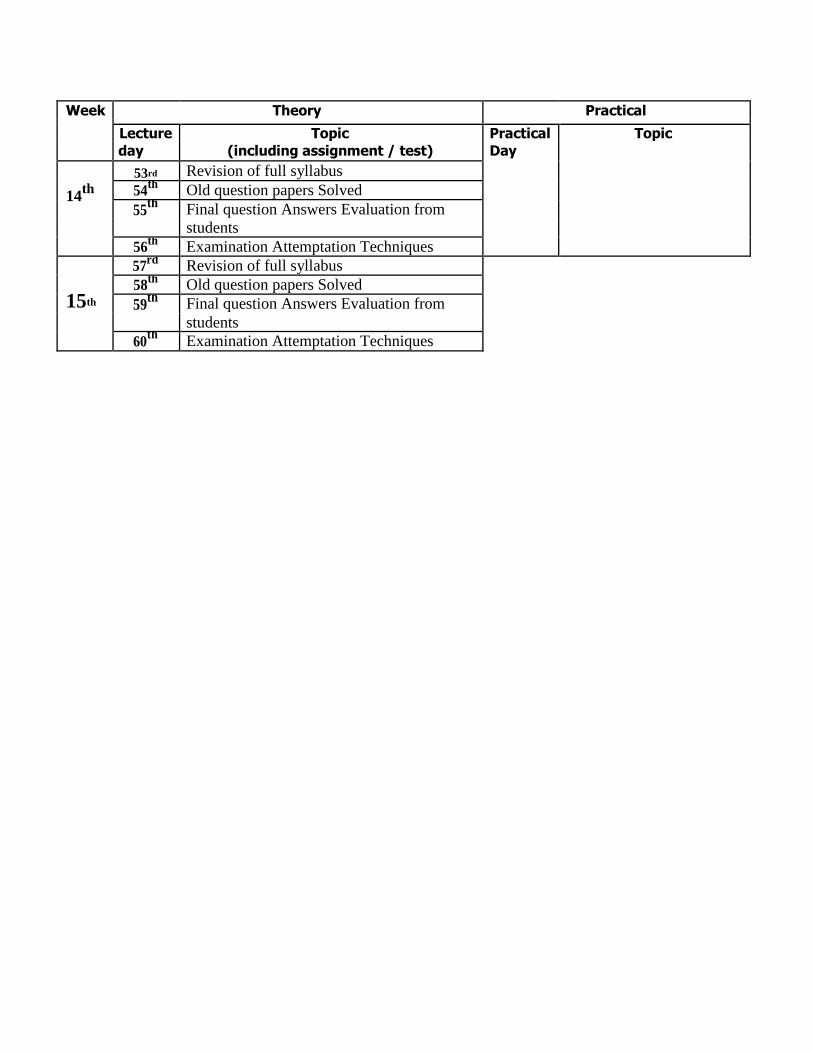
Week Theory Practical
Lecture Topic Practical Topic
day (including assignment / test) Day
53rd Revision of full syllabus
14th 54
th Old question papers Solved
55th Final question Answers Evaluation from
students
56th Examination Attemptation Techniques
57rd Revision of full syllabus
15th
58th Old question papers Solved
59th Final question Answers Evaluation from
students
60th
Examination Attemptation Techniques
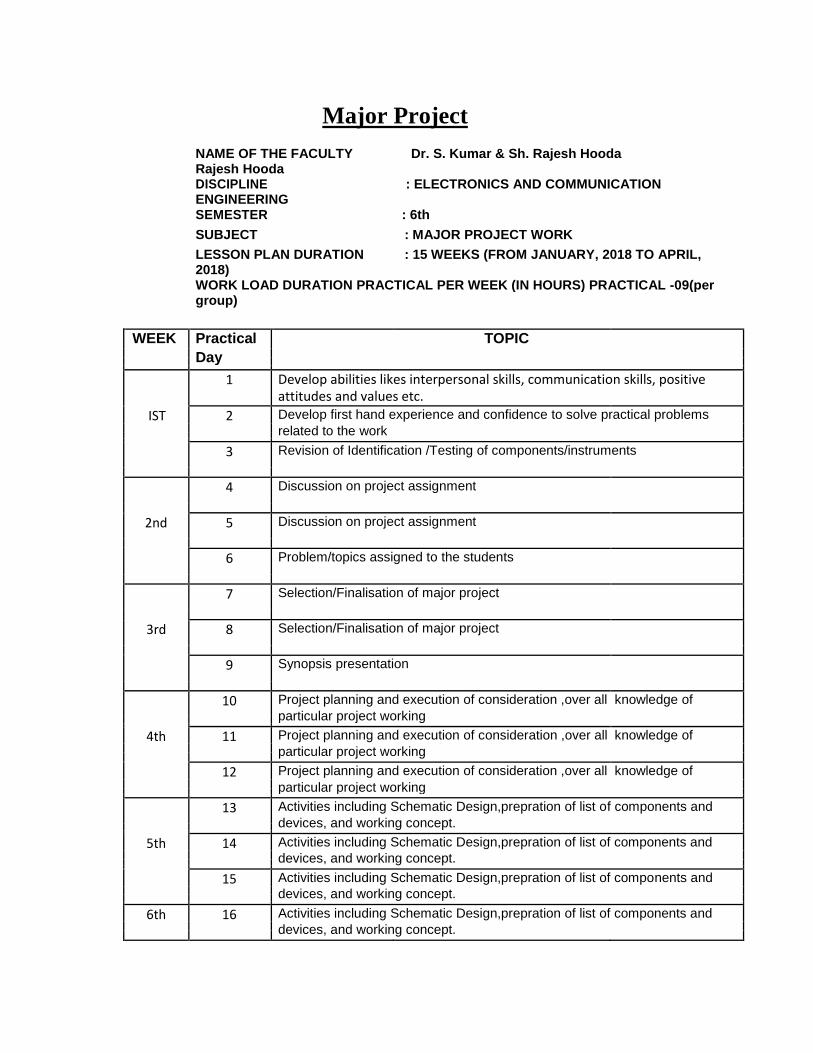
Major Project
NAME OF THE FACULTY Dr. S. Kumar & Sh. Rajesh Hooda Rajesh Hooda
DISCIPLINE : ELECTRONICS AND COMMUNICATION ENGINEERING
SEMESTER : 6th
SUBJECT : MAJOR PROJECT WORK LESSON PLAN DURATION : 15 WEEKS (FROM JANUARY, 2018 TO APRIL, 2018)
WORK LOAD DURATION PRACTICAL PER WEEK (IN HOURS) PRACTICAL -09(per group)
WEEK Practical TOPIC Day
1 Develop abilities likes interpersonal skills, communication skills, positive attitudes and values etc.
IST 2 Develop first hand experience and confidence to solve practical problems
related to the work
3 Revision of Identification /Testing of components/instruments
4 Discussion on project assignment
2nd 5 Discussion on project assignment
6 Problem/topics assigned to the students
7 Selection/Finalisation of major project
3rd 8 Selection/Finalisation of major project
9 Synopsis presentation
10 Project planning and execution of consideration ,over all knowledge of particular project working
4th 11 Project planning and execution of consideration ,over all knowledge of
particular project working
12 Project planning and execution of consideration ,over all knowledge of particular project working
13 Activities including Schematic Design,prepration of list of components and devices, and working concept.
5th 14 Activities including Schematic Design,prepration of list of components and
devices, and working concept.
15 Activities including Schematic Design,prepration of list of components and devices, and working concept.
6th 16 Activities including Schematic Design,prepration of list of components and
devices, and working concept.
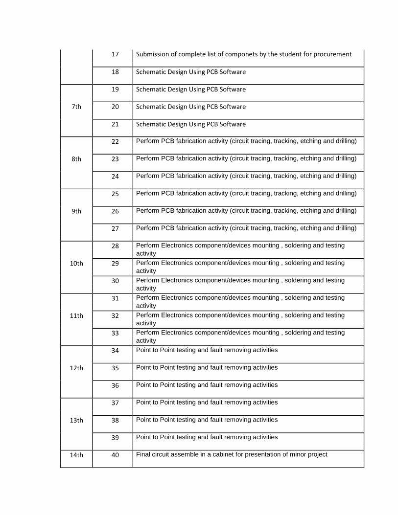
17 Submission of complete list of componets by the student for procurement
18 Schematic Design Using PCB Software
19 Schematic Design Using PCB Software
7th 20 Schematic Design Using PCB Software
21 Schematic Design Using PCB Software
22 Perform PCB fabrication activity (circuit tracing, tracking, etching and drilling)
8th 23 Perform PCB fabrication activity (circuit tracing, tracking, etching and drilling)
24 Perform PCB fabrication activity (circuit tracing, tracking, etching and drilling)
25 Perform PCB fabrication activity (circuit tracing, tracking, etching and drilling)
9th 26 Perform PCB fabrication activity (circuit tracing, tracking, etching and drilling)
27 Perform PCB fabrication activity (circuit tracing, tracking, etching and drilling)
28 Perform Electronics component/devices mounting , soldering and testing activity
10th 29 Perform Electronics component/devices mounting , soldering and testing
activity
30 Perform Electronics component/devices mounting , soldering and testing activity
31 Perform Electronics component/devices mounting , soldering and testing activity
11th 32 Perform Electronics component/devices mounting , soldering and testing
activity
33 Perform Electronics component/devices mounting , soldering and testing activity
34 Point to Point testing and fault removing activities
12th 35 Point to Point testing and fault removing activities
36 Point to Point testing and fault removing activities
37 Point to Point testing and fault removing activities
13th 38 Point to Point testing and fault removing activities
39 Point to Point testing and fault removing activities
14th 40 Final circuit assemble in a cabinet for presentation of minor project
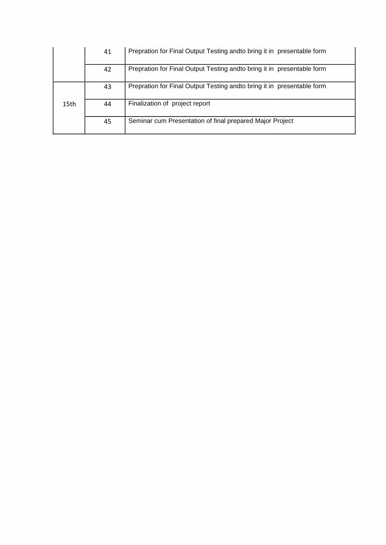
41 Prepration for Final Output Testing andto bring it in presentable form
42 Prepration for Final Output Testing andto bring it in presentable form
43 Prepration for Final Output Testing andto bring it in presentable form
15th 44 Finalization of project report
45 Seminar cum Presentation of final prepared Major Project
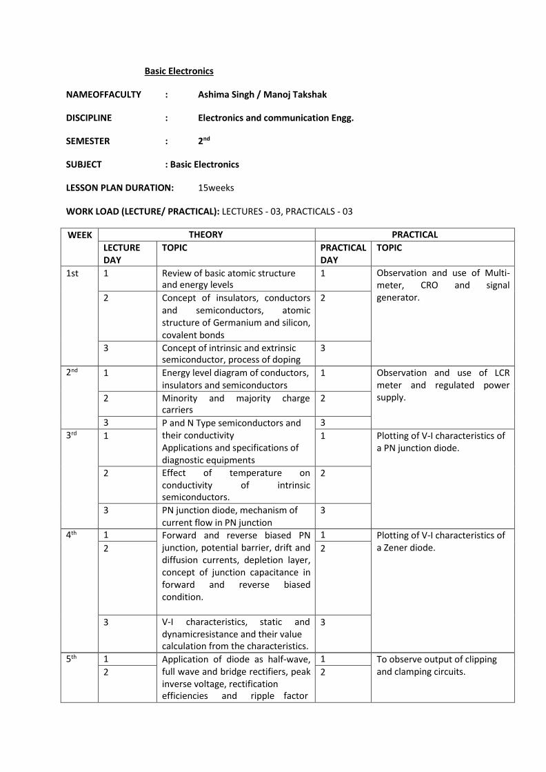
Basic Electronics
NAMEOFFACULTY : Ashima Singh / Manoj Takshak
DISCIPLINE : Electronics and communication Engg.
SEMESTER : 2nd
SUBJECT : Basic Electronics
LESSON PLAN DURATION: 15weeks
WORK LOAD (LECTURE/ PRACTICAL): LECTURES - 03, PRACTICALS - 03
WEEK THEORY PRACTICAL
LECTURE DAY
TOPIC PRACTICAL DAY
TOPIC
1st 1 Review of basic atomic structure and energy levels
1 Observation and use of Multi- meter, CRO and signal generator. 2 Concept of insulators, conductors
and semiconductors, atomic structure of Germanium and silicon, covalent bonds
2
3 Concept of intrinsic and extrinsic semiconductor, process of doping
3
2nd 1 Energy level diagram of conductors, insulators and semiconductors
1 Observation and use of LCR meter and regulated power supply. 2 Minority and majority charge
carriers 2
3 P and N Type semiconductors and their conductivity Applications and specifications of diagnostic equipments
3
3rd 1 1 Plotting of V-I characteristics of a PN junction diode.
2 Effect of temperature on conductivity of intrinsic semiconductors.
2
3 PN junction diode, mechanism of current flow in PN junction
3
4th 1 Forward and reverse biased PN junction, potential barrier, drift and diffusion currents, depletion layer, concept of junction capacitance in forward and reverse biased condition.
1 Plotting of V-I characteristics of a Zener diode. 2 2
3 V-I characteristics, static and dynamicresistance and their value calculation from the characteristics.
3
5th 1 Application of diode as half-wave, full wave and bridge rectifiers, peak inverse voltage, rectification efficiencies and ripple factor
1 To observe output of clipping and clamping circuits. 2 2
calculation.
3 Shunt capacitor filter, series inductor filter, LC and πfilters.
3
6th 1 Types of diodes, characteristics and applications of zener diodes, zener and avalanche breakdown
1 Measurement of voltage gain, input and output impedance in a single stage amplifiercircuit.
2 2
3 Clipping and clamping circuits 3 7th 1 Concept of a bipolar transistor, its
structure, PNP and NPN transistors, their symbols and mechanism of current flow; Current relations in a transistor, concept of leakage current.
1 Design of half-wave rectifier circuit using one diode on breadboard..
2 2
3 3
8th 1 CB, CE, CC configurations of a transistor; input and output characteristics in CB and CE configurations; input and output dynamic resistance in CB and CE configurations; Current amplification factors.Comparison of CB, CE and CC configurations.
1 Design of full-wave rectifier circuit using two diodes on breadboard.
2 2
3 3
9th 1 Transistor as an amplifier in CE configuration; concept of DC load line and calculation of current gain and voltage gain using DC load line.
1 Design of bridge-rectifier circuit using four diodes on breadboard.
2 2
3 3
10th 1 1 Plotting of the wave shape of full wave rectifier with shunt capacitorfilter.
2 Concept of transistor biasing and selection of operating point.
2
3 Need for stabilization of operating point
3
11th 1 Different types of biasing circuits. 1 Plotting of the wave shape of full wave rectifier with series inductorfilter.
2 2
3 Single stage transistor amplifier circuit
3 12th 1 1 Plotting of input and output
characteristics and calculation of parameters of transistorsin CE configuration.
2 Concept of dc and ac load line and its use
2
3 3
13th 1 1 Plotting of input and output characteristics and calculation of parameters of transistors in CBconfiguration.
2 Explanation of phase reversal of output voltage with respect to input voltage
2
3 Construction, operation and characteristics of a MOSFET in depletion and enhancement modes and its applications.
3 14th 1 1 Plotting of V-I characteristics of
a FET based amplifier. 2 2 3 3
15th 1 CMOS - advantages and applications
1
2 2
3 Comparison of JFET, MOSFET, BJT 3
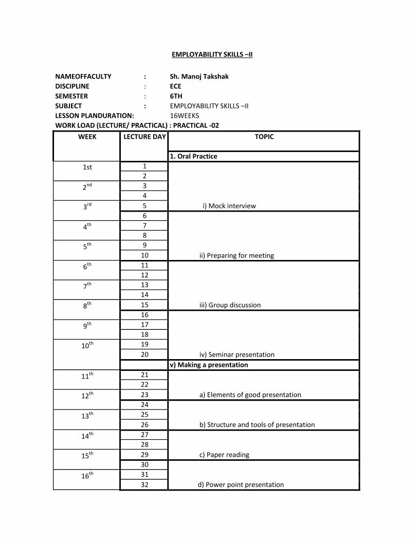
EMPLOYABILITY SKILLS –II
NAMEOFFACULTY : Sh. Manoj Takshak
DISCIPLINE : ECE
SEMESTER : 6TH
SUBJECT : EMPLOYABILITY SKILLS –II
LESSON PLANDURATION: 16WEEKS
WORK LOAD (LECTURE/ PRACTICAL) : PRACTICAL -02
WEEK LECTURE DAY TOPIC
1. Oral Practice
1st 1
i) Mock interview
2
2nd 3
4
3rd 5
6
ii) Preparing for meeting
4th 7
8
5th 9
10
6th 11
iii) Group discussion
12
7th 13
14
8th 15
16
iv) Seminar presentation
9th 17
18
10th 19
20 v) Making a presentation
11th 21
a) Elements of good presentation
22
12th 23
24
b) Structure and tools of presentation
13th 25
26
14th 27
c) Paper reading
28
15th 29
30
d) Power point presentation
16th 31
32


