
31 | P a g e
Thin Film Deposition Technique
Physical Chemical
1. Resistive Heating 2. Flash Evaporation 3. Electron Beam
Evaporation 4. Laser
Evaporation 5. Arc Evaporation 6. Radio Frequency
(RF)Heationg
1. Glow Discharge Sputtering
2. Triode Sputtering 3. RF Sputtering 4. Magnetron
Sputtering 5. Face Target
Sputtering 6. Ion Beam
Sputtering 7. A.C. Sputtering
1. Chemical Vapour Deposition (CVD)
2. Laser CVD 3. Photo CVD 4. Plasma Enhanced
CVD 5. Metal Organo
CVD (MOCVD) 6. Atmospheric
Pressure CVD
1. Electro Deposition 2. Electroless
Deposition 3. Spray Pyrolysis 4. Sol Gel Process 5. SILAR 6. Solution Growth
Technique 7. Anodization 8. Liquid Phase
Epitaxy
2.1 FILM FORMATION TECHNIQUE:
The Physical properties of polymer film basically depend on the film
preparation/formation technique. There are several methods that can be used for
formation of polymer thin film. The formation of synthetic polymer is a process
which occurs via chemical connection of many hundred to thousand of monomer
molecules. As a result, macromolecule is formed [1,2]. The important thin film
formation processes are based on liquid phase chemical techniques, gas phase
chemical processes, glow discharge processes and evaporation methods [3]. The
methods employed for thin film deposition can be divided into two groups based on
the nature of deposition process, namely physical or chemical as shown in Fig. 2.1.
Fig.2.1 Classification of Thin Film Deposition Technique
The details of all physical methods are beyond the scope of this dissertation.
Chemical deposition techniques are the most important methods for growth of the
films owing to their versatility for depositing large number of elements and
compounds at low temperature [4]. The chemical deposition process is economically
Vacuum Sputtering Gas Phase Liquid Phase

32 | P a g e
effective and has been industrially exploited to large scale. Brief ideas about some
important physical and chemical methods of thin film formation are mentioned here
for general understanding.
2.1.1 Physical Vapor Deposition (PVD) Processes
Physical vapor deposition is a technique whereby physical process, such as
evaporation, sublimation or ionic impingement on a target, facilitates the transfer of
atoms from a solid or molten source onto a substrate. Evaporation and sputtering are
the most widely used PVD methods for depositing films [5]. Typically, PVD
processes are used to deposit films with thicknesses in the range of a few nanometers
to thousand of nanometers; however, they can also be used to form multilayer
coatings graded composition deposits, very thick deposits and freestanding structures.
The substrates can range in size from very small to very large such as the 10' × 12'
glass panels used for architectural glass. The substrates can range in shape from flat to
complex geometries such as watchbands and tool bits. Typical PVD deposition rates
are 10-100Å (1-10 nanometers) per second.
PVD processes can be used to deposit films of elements and alloys as well as
compounds using reactive deposition processes. In reactive deposition processes,
compounds are formed by the reaction of depositing material with the ambient gas
environment such as nitrogen (e.g. titanium nitride, TiN) or with a co-depositing
material (e.g. titanium carbide, TiC). Quasi-reactive deposition is the deposition of
films of a compound material from a compound source where loss of the more
volatile species or less reactive species during the transport and condensation process,
is compensated for by having a partial pressure of reactive gas in the deposition
environment. For example, the quasi-reactive sputter deposition of ITO (indium-tin-
oxide) from an ITO sputtering target using a partial pressure of oxygen in the plasma.
The main categories of PVD processing are vacuum evaporation, sputter deposition,
arc deposition and ion plating as depicted in Fig. 2.2.
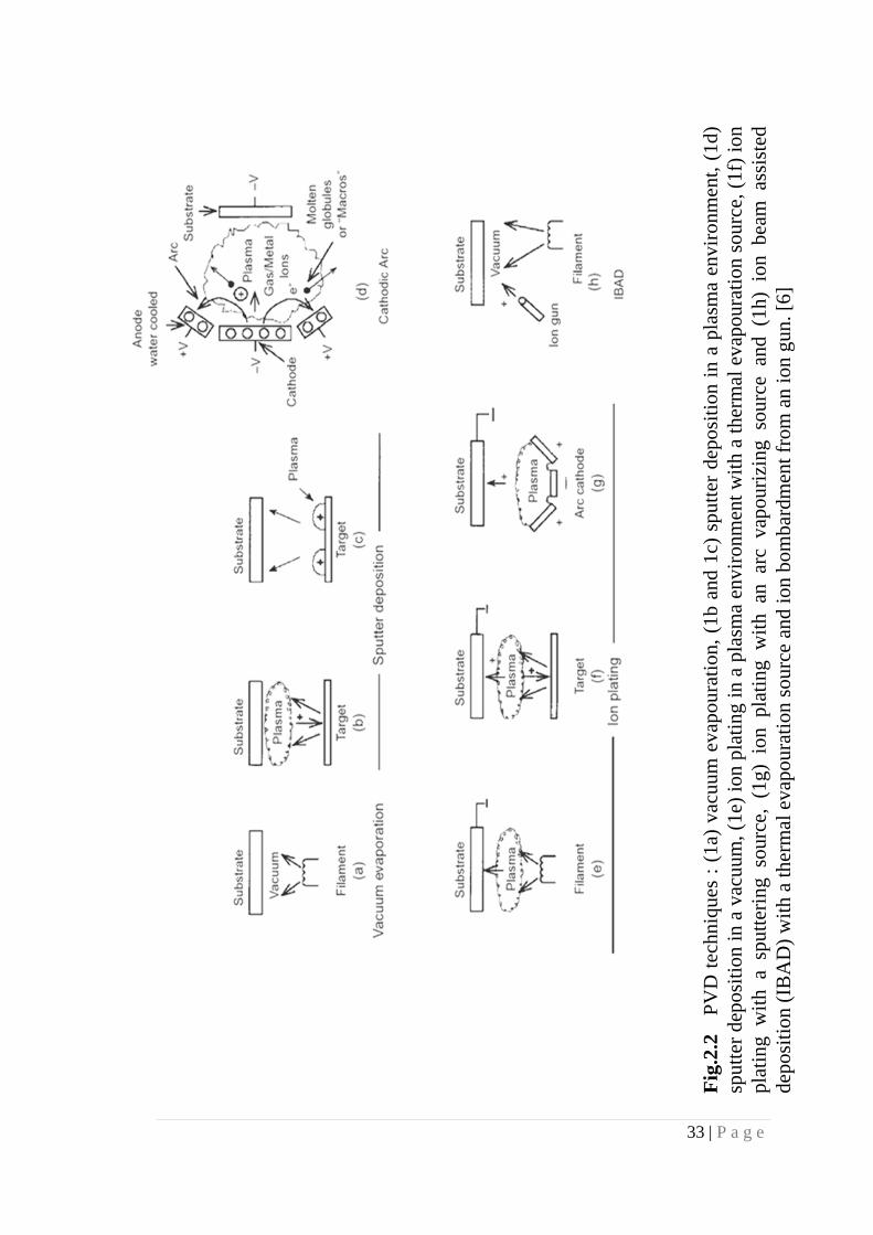
33
Fig
22
PV
Dte
chni
ques
:(1
a)va
cuum
evap
oura
tion
(1b
and
1c)
sput
ter
depo
siti
onin
apl
asm
aen
viro
nmen
t(1
d)
| P a g e
Fig
.2.2
P
VD
tec
hniq
ues
: (1
a) v
acuu
m e
vapo
urat
ion,
(1b
and
1c)
spu
tter
dep
osit
ion
in a
pla
sma
envi
ronm
ent,
(1d)
sp
utte
r de
posi
tion
in a
vac
uum
, (1e
) io
n pl
atin
g in
a p
lasm
a en
viro
nmen
t wit
h a
ther
mal
eva
pour
atio
n so
urce
, (1f
) io
n pl
atin
g w
ith
a sp
utte
ring
sou
rce,
(1g
) io
n pl
atin
g w
ith
an a
rc v
apou
rizi
ng s
ourc
e an
d (1
h) i
on b
eam
ass
iste
d de
posi
tion
(IB
AD
)w
ith
ath
erm
alev
apou
rati
onso
urce
and
ion
bom
bard
men
tfro
man
ion
gun.
[6]
depo
siti
on (
IBA
D)
wit
h a
ther
mal
eva
pour
atio
n so
urce
and
ion
bom
bard
men
t fro
m a
n io
n gu
n. [
6]

34 | P a g e
A. Vacuum deposition
Vacuum deposition which is sometimes called vacuum evaporation is a PVD
process in which material from a thermal vaporization source reaches the substrate
with title or no collision with gas molecules in the space between the source and
substrate. The trajectory of the vaporized material is “line-of-sight”. The vacuum
environment also provides the ability to reduce gaseous contamination in the
deposition system to a low level. Typically, vacuum deposition takes place in the gas
pressure range of 10-5 to 10-9 Torr depending on the level of gaseous contamination
that can be tolerated in the deposition system. The thermal vapourization rate can be
very high compared to other vapourization methods. The material vapourized from
the source has a composition which is in proportion to the relative vapour pressure of
the material in the molten source material. Thermal evaporation is generally done
using thermally heated sources such as tungsten wire coils or by high energy electron
beam heating of the source material itself. Generally the substrates are mounted at an
appreciable distance away from the vapourization source to reduce radiant heating of
the substrate by the vapourization source.
Vacuum deposition is used to form optical interference coating, mirror
coating, decorative coatings, permeation barrier film on flexible packaging materials,
electrically conducting films, wear resistant coatings, and corrosion protective
coatings.
B. Sputter deposition
Sputter deposition is the deposition of particles vapourized from a surface
(“target”), by the physical sputtering process. Physical sputtering is a non-thermal
vapourization process where surface atoms are physically ejected from a solid surface
by momentum transfer from an atomic sized energetic bombarding particles which is
usually a gaseous ion accelerated from a plasma. This PVD process is sometimes just
called sputtering i.e. “Sputtered films of –” which is an improper term in that the film
is not being sputtered. Generally the source-to-substrate distance is short compared to
vacuum deposition. Sputter deposition can be performed by energetic ion
bombardment of a solid surface (sputtering target) in vacuum using an ion gun or low
pressure plasma (<5 m Torr) where the sputtered particles suffer few or no gas phase

35 | P a g e
collisions in the space between the target and the substrate. Sputtering can also be
done in a higher plasma pressure (5-30 m Torr) where energetic particles sputtered or
reflected from the sputtering target are “thermalized” by gas phase collisions before
they reach the substrate surface. The plasma used in sputtering can be confined near
the sputtering surface or may fill the region between the source and the substrate. The
sputtering source can be an element, alloy mixture, or a compound and the material is
vapourized with the bulk composition of the target. The sputtering target provides a
long lived vapourization source that can be mounted so as to vapourize in any
direction. Compound materials such as titanium nitride (TiN) and zirconium nitride
(ZrN) are commonly reactively sputter deposited by using a reactive gas in the
plasma. The presence of the plasma “activities” the reactive gas (“plasma activation”)
making it more chemically reactive.
Sputter deposition is widely used to deposit thin film metallization on
semiconductor material, coatings on architectural glass, reflective coatings on
compact discs, magnetic films, dry film lubricants and decorative coatings.
C. ARC vapour deposition
Arc vapour deposition uses a high current, low-voltage arc to vapourize a
cathodic electrode (cathodic arc) on anodic electrode (anodic arc) and deposit the
vapourized material on a substrate. The vapourized material is highly ionized and
usually the substrate is biased so as to accelerate the ions (“film ions”) to the substrate
surface.
D. Ion plating
Ion plating which is sometimes called Ion Assisted Deposition (IAD) or Ion
Vapour Deposition (IVD) utilizes concurrent or periodic bombardment of the
depositing film by atomic-sized energetic particles, to modify and control the
properties of the depositing film. In ion plating the energy, flux and mass of the
bombarding species along with the ratio of bombarding particles are important
processing variables. The deposition material may be vapourized either by
evaporation, sputtering, arc erosion or by decomposition of a chemical vapour
precursor. The energetic particles used for bombardment are usually ions of an inert

36 | P a g e
or reactive gas, or, in some cases, ions of the condensing film material (“film ions”).
Ion plating can be done in a plasma environment where ions for bombardment are
extracted from the plasma or it may be done in a vacuum environment where ions for
bombardment are formed in a separate “ion gun”. The latter ion plating configuration
is often called Ion Beam Assisted Deposition (IBAD). By using a reactive gas in the
plasma, films of compound materials can be deposited. Ion plating can provide dense
coatings at relatively high gas pressures where gas scattering can enhance surface
coverage. Ion plating is used to deposit hard coating of compound materials, adherent
metal coatings, optical coating with high densities, and conformal coatings on
complex surfaces.
2.1.2 Chemical Vapour Deposition
Chemical vapour deposition (CVD) processes are widely used in industry due
to their versatility for depositing a very large variety of elements and compounds
covering a wide range from amorphous deposits to epitaxial layers having high degree
of perfection and purity.
CVD can be defined as a process in which the gaseous chemical reactants are
transported to the reaction chamber, activated thermally (conventional CVD) or by
other than thermal means (plasma assisted CVD or laser induced CVD), in the
vicinity of the substrate, and made to react to form a solid deposit on the substrate
surface. It is possible to deposit films of uniform thickness and low porosity even on
substrates of complicated shape in this process.
A major area for utility of CVD is in microelectronics applications, such as
gate insulating layers, passivation layers, oxidation barrier, polycrystalline silicon, etc.
CVD techniques are also extensively employed for protective coating for a variety of
operating environments where, for example, protection is required against wear,
erosion, and high temperature oxidation [7]. CVD has numerous other names and
adjectives associated with it such as Vapour Phase Epitaxy (VPE) when CVD is used
to deposit single crystal films, Metal-organic CVD (MOCVD) when the precursor gas
is a metal-organic species, Plasma Enhanced CVD (PECVD) when a plasma is used
to induce or enhance decomposition and reaction, and Low Pressure CVD (LPCVD)
when the pressure is less than ambient.

37 | P a g e
Plasmas can be used in CVD reactors to activate and partially decompose the
precursor species. This allows deposition at a temperature lower than thermal CVD
and the process is called plasma-enhanced CVD (PECVD) or plasma-assisted CVD
(PACVD) [8,9]. The plasmas are typically generated by radio-frequency techniques.
At low pressures, concurrent energetic particle bombardment during deposition can
affect the properties of films deposited by PECVD [10].
Plasma based CVD are also used to deposit polymer film (Plasma
polymerization) [11]. In this case the precursor vapour is a monomer that becomes
cross linked in the plasma and on the surface to form an organic or inorganic polymer
film. These films have very low porosity and excellent surface coverage. When
plasma depositing films from organo-silane precursors, oxygen can be added to the
plasma to oxidize more or less of the silicon in the film [12].
2.1.3 Electroplating, Electroless Plating and Displacement Plating
Electroplating is the deposition on the cathode of metallic ions from the
electrolyte of an electrolysis cell [13, 14]. Only about 10 elements (Cr, Ni, Zn, Sn, In,
Ag, Cd, Au, Pb, and Rh) are commercially deposited from aqueous solutions. Some
alloy composition such as Cu-Zn, Cu-Sn, Pb-Sn, Au-Co, Sn-Ni, Ni-Fe, Ni-P and Co-P
are commercially deposited, Conductive oxides such as PbO2 and Cr2O3 can also be
deposited by electroplating. A thin film of material deposited by electroplating is
often called a “flash” and is on the order of 40 thousandths of an inch thick. Typically,
the anode of the electrolytic cell is of the material to be deposited and is consumed in
the deposition process. In some cases, the anode material is not consumed and the
material to be deposited comes only from solution. For example, lead oxide, PbO2 can
be electrodeposited from a lead nitrate plating bath using carbon anodes. Stainless
steel and platinum are also often used as non consumable anode materials.
In electroless or autocatalytic plating no external voltage/current source is
required. The voltage/current is supplied by the chemical reduction of an agent at the
deposit surface. The reduction reaction is catalyzed by a material, which is often
boron or phosphorous. Materials that are commonly deposited by electroless
deposition are Ni, Cu, Au, Pd, Pt, Ag, Co and Ni-Fe alloys. Displacement plating is
the deposition of ions in solution on a surface and results from the difference in

38 | P a g e
electro negativity of the surface and the ions. Electrophoresis is the migration of
charged particles in an electric field. Electrophoretic deposition, or electrocoating, is
the electro deposition of large charged particles from a solution [15,16]. The particles
may be charged dielectric particles (glass particles, organic molecules, paint globules,
etc.) which are non soluble in the aqueous electrolyte. Alternatively some of the
components can be treated so that they are soluble in water but will chemically react
in the vicinity of an electrode and their solubility is decreased. Particles are usually
deposited on the anode but sometimes on the cathode.
2.1.4 Films from Polymer Solution
The techniques of film formation described above are not expected to give
useful films for research purposes. Further, the polymer films formed by these
techniques may have different degree of polymerisation and may contain undesired
impurities." Polymer films formed by vacuum deposition technique are also not quite
useful as these have pin holes. Films of doped polymer cannot be obtained by above
mentioned methods since it is difficult to control the quality of dopant both during
evaporation as well as during polymerisation. Film with uniform degree of
polymerisation and high purity can be prepared from polymer solution using highly
pure polymer as solute and inert solvents of AR grade. The doping percentage can be
controlled easily by dissolving known amount of dopant in the solution.
There are two main methods available for preparing thin films from polymer
solution:
A. Isothermal immersion technique
Solution of suitable concentration is kept at a desired temperature and
substrate is immersed into it vertically for a given period of time depending upon the
required film thickness. When the film is deposited, the substrate is slowly taken out
and dried by hot air. The deposited film is then gently detached using a sharp knife
edge [17]. Doped films can also be prepared using desired quantity of dopant in
solution. Rastogi and Chopra [18] found that the thickness of film depends upon
concentration of the solution, its temperature, nature of the substrate, and the time for
which the substrate is kept immersed in the solution. This method requires a great

39 | P a g e
care in selecting the temperature and concentration of the solution. Also, sophisticated
mechanical instrumentation is required for taking out the substrate from the solution
and keeping them exactly vertical to the solution surface. Lack of proper
instrumentation and precautions may result into the films containing air bubbles and
nonuniform thickness.
B. Casting from the solution
Polymer solution of known concentration and quantity is spread over plane
clear glass plate of known surface area which is made to float in a mercury pool.
Solvent is allowed to evaporate at a suitable constant temperature and the resulting
film is gently detached from the substrate. Films of different thickness may be
obtained using solution of different concentrations [19]. The films obtained by this
technique are of uniform thickness and perfectly plane. Also, an elaborate cleaning
procedure must be adopted for substrate in order to eliminate any possible impurity
and deformation.
In the present investigation, plane glass plates were used as substrate for
deposition of polymer films. The glass plates were cleaned carefully by acid, water
and finally in soap water. Subsequently, these were rinsed in the distilled water. The
cleaned substrates were then dried up in hot air.
2.2 PREPARATION OF PURE PVA, PALM LEAF POWDER AND THEIR
POLYMER BIOCOMPOSITE FILM SAMPLES
The 98% acetalized Poly vinyl alcohol (PVA) with molecular weight of 1400
was procured from M/S Chemical Industries, Mumbai, India and used without further
purification. The Alexander Palm leaf has been obtained from Jawaharlal Nehru
Agriculture University, Jabalpur, M.P., India. The obtained green leaves were made to
dry at room temperature, after that these were grinded and fine powder of palm leaves
was obtained for further use. This powder was stored in to desiccators to avoid the
effect of moisture and other environmental fluctuations/conditions.
The PVA-Palm leaf films of following weight percentage were prepared for the
present investigation:
40 | P a g e
(i) Pure PVA (0.0 wt%PL+PVA)
(ii) 5 wt% Palm Leaf Powder+PVA (5%PL+PVA)
(iii) 10 wt% Palm Leaf Powder+PVA (10%PL+PVA)
(iv) 15 wt% Palm Leaf Powder+PVA (15%PL+PVA)
(v) 20 wt% Palm Leaf Powder+PVA (20%PL+PVA)
For this pure PVA and Palm leaf powder were weighed for their desired ratio.
These were then mixed and dissolved in deionized water. This solution was stirred at
40°C in a magnetic stirrer for a minimum time of four hours. Thereafter, the
homogeneous solution thus obtained was poured over the glass plates floating in the
mercury pools kept inside the oven. The oven temperature was maintained between
40-50 oC. Great care was taken to avoid air bubbles during the settling of polymer
solution over the plates. After the film was formed the glass plates were taken out
carefully. Pure PVA polymer film and Palm leaf powder reinforced biocomposite
films of about 50 to 250 µm in thickness were prepared by this solvent cast technique
for various characterizations. The films were preserved in desicator so that these are
not damaged.
2.3 MEASUREMENT OF FILM THICKNESS
The thickness of a thin film is its most important characteristic feature and
thickness measurements are therefore of primary importance in any thin film
investigation. Various film thickness measurement techniques have been developed
over the years. Out of which some are listed below. Each method has its limitations
and may not be suitable for routine measurements. A qualitative description and
associated limitations of the following class of techniques is given here:
(i) Mechanical methods
(ii) Optical methods
(iii) Electrical methods
2.3.1 Mechanical Methods
This includes three important methods namely stylus method, weighing
method and micrometer gauge method.

41 | P a g e
A. Stylus method
A diamond tip is moved along the film surface while its vertical displacement
is electronically enlarged by a factor of 106 and recorded. From the film edge the
thickness is found directly as the step height detected by the stylus [20, 21].
B. Weighing method
This method depends on the increase of the weight of a film due to its mass
increase and from the knowledge of its density and the deposited area; film thickness
(d or t) can be evaluated form the relation
2.1
where W is the weight difference of the film, is its density and A is the
deposited area. The increase in the film weight can be measured by a suitable
microbalance [22, 23]
C. Micrometer gauge method
This technique allows a direct thickness measurement. The film surfaces are
never ideally flat; the thickness is usually specified as a mean thickness. This concept
allows one to define an average thickness for even a discontinuous film. In this
method of measurement of the film thickness a micrometer is used. Generally, a
number of observations are taken and they are averaged to find out the exact
thickness. During the present investigation, the author has used this method for
determining the thickness of the film. A highly accurate micrometer screw gauge with
the least count 0.001mm, manufactured by M/S Mitutoys Mfg. Co. Ltd., Japan, was
used.
2.3.2 Optical Methods
Optical techniques for film thickness determinations are widely used for a
number of reasons. They are applicable to both opaque and transparent films, yielding
thickness values of generally high accuracy. In addition, measurements are quickly
performed, frequently nondestructive, and utilize inexpensive equipment.

42 | P a g e
A. Photometric method
This method depends on the change in the transmittance of light at normal
incidence with the increase of film thickness as given by the Lambert law
2.2
where is the absorption coefficient and t is the film thickness. I and Io are
respectively, the intensity of transmittance and incident monochromatic light. A
transmittance (T = I/Io) versus film thickness graph on a semi-log scale will be a
straight line. Thus it is possible to correlate film thickness with transmittance. This
technique can be used for absorbing as well as semi-absorbing films provided the
deposition parameters have no effect on the transmittance of the films. However, in
many cases it is not so and hence this technique is not suitable except for a few cases.
For transparent films is 0 or negligible and hence this method is not applicable.
B. Ellipsometric method
Ellipsometry is a commonly used non-destructive technique to characterize
thin films [24, 25] Ellipsometry is a very powerful and accurate optical method to
measure the thickness of thin films. This technique involves the use of a polarized
light for reflection from a film on a substrate at a non-normal incidence but preferably
at an angle of incidence of 45o. A reflection from an absorbing film will cause a
change both in the relative amplitude of the two perpendicular components of the
reflection viz. parallel to the plane of incidence and perpendicular to the plane of
incidence, leading to an elliptically polarized light. An ellipsometer is an instrument
by the different parameters of the elliptically polarized reflected beam can be
measured and from these data film thickness can be evaluated. In this method a
complicated mathematical analysis is required and therefore is not generally used
[26].
C. Interferometry
Film thickness can be measured using interferometry [27]. It can also be
measured accurately from interference fringes using multiple beam interferometry
[28] and also from the fringes of equal chromatic order (FECO) techniques. In the
43 | P a g e
former case two reflecting surfaces are brought in close proximity such that a small
wedge with a small air gap in between them is formed. If a monochromatic light is
now incident on them at normal incidence, then an interference of light due to
interactions of multiple reflected beams in air gap will take place resulting in a series
of fringes which can be observed in the back reflected light. The distance between the
fringes or lines depends on the air gap as well as one the wave length of the
monochromatic light. This principle is adopted and suitably modified for the multiple
beam interferometric method of the measurement of film thickness [29]. After
obtaining a set of sharp fringes, the thickness (t) can be determined uing the relation
/2 2.3
Where b is the displacement of the fringes at the step and a is the distance between
consecutive fringes. The fringe displacements which are in the form of parallel lines,
however, occur at the film edge.
D. Light sectioning method
A device known as a light-section microscope (Carl Zeiss, Oberkochen,
Germany) is available which non-destructively measure the thickness of transparent
films allowing the determination of film thickness at selected regions on substrate
surfaces. It allows analysis of the variation in film thickness and an estimate of
surface roughness without physical contact with the surface [30].
An incandescent lamp of variable brightness illuminates a slit which projects a
narrow band of light through an objective at an angle of 45o to the plane of the surface
being measured. Some of the light is reflected from the surface of film; the remainder
penetrates the film and is reflected from the surface of substrate or core. In the
eyepiece of the microscope at the opposite 45o angle, the profiles of the film and
substrate or core can be seen coincidently as a series of peaks and troughs after the
band of light has been reflected/refracted at the sample. A cross-line graticule in the
eyepiece can be moved within the field of view by means of a graduated measuring
drum. The required distance values can then be read off with the drum with a
sensitivity of 0.1 µm over longitudinal or transversal movements of upto 25mm. For

44 | P a g e
measurement of film thickness, this technique is restricted therefore to transparent
films.
E. Other methods
There are several other methods which are less universal and can be used for
some specific cases and some of them are eminently suitable for mass or routine
productions. In some of them the basic assumption is that the film properties such as
resistance, capacitance, hall voltage, etc. are dependent only on the film thickness, but
not on deposition conditions. Such a criterion may be satisfied only in routine of mass
production cases where a standard procedure is adopted. Since film properties are
dependent also on the deposition parameters the methods depending on the above
properties are used in specific cases only and for restricted thickness range.
Film thickness can also be estimated from its absorption property of radiation
such as light, X-rays, -ray, -rays, electron beam etc. and the absorption is generally
an exponential function of the film thickness. Absorption of X-rays, and -rays by a
material takes place when these are allowed to pass through it. This property is then
used for the determination of the thickness of the material and can be used say
between about 100 Å to about 1 mm of thickness. High velocity electron beam say
between 50 kV to 100 kV can be used for measuring film thickness of about a few
thousand Å. In the later method electron absorption is measured when the Bragg
reflection is absent. The back scattering of and -rays by a material, X-rays
fluorescence, electron microprobe methods etc. are also used for measuring film
thickness, though some of these are not straight forward and involve the measurement
of the mass of the material.
2.3.3 Electrical Method
In this method vacuum evaporated electrodes are deposited on both the
surfaces of the film specimen and the capacitance of the film condenser so formed is
measured using a sensitive LCR bridge [31]. If the high frequency dielectric constant,
area of the metallic electrodes, etc. are known then the thickness of the sample can be
very accurately known provided the film is of uniform thickness with no pin holes.
This method, therefore, is the most suitable for solution grown samples.

45 | P a g e
2.4 ELECTRODES (Types of Contacts)
The polymer electrode contact plays an important role in all electrical
measurements [31, 32]. The shape of energy band near dielectric electrode interface
decides which one of the three categories of contacts is at work. When energy band is
completely horizontal, it is called a neutral contact; if a band bends downwards
helping in injection of carriers of the opposite sign then the electrode is an ohmic
electrode; when the energy band bends upwards hindering the injection and
neutralisation of charges, the contact made is called a blocking contact.
Following four types of electrodes can be used for making electrical contacts
with polymer films for the purpose of studying the charging and discharging
phenomena:
(a) Painted electrodes,
(b) Liquid contact electrodes,
(c) Vacuum deposited electrodes, and
(d) Pressed metal foil electrodes.
2.4.1 Painted Electrodes
Conducting material paste can be used for painting the polymer film and can
be used as the electrodes. Such materials are graphite, silver and epoxy paints.
However, such paints may react with the polymer and can damage it also. Therefore,
use of such painted electrodes is restricted to only those polymers which do not react
with these.
2.4.2 Liquid Contact Electrodes
In this, non-metallised surface of a unilaterally metallised film specimen is
kept in contact with a liquid, such as water or ethyl alcohol so that a thin uniform
layer of liquid rests over the film surface. A potential is applied between the metallic
electrode and rear unmetallised surface of the film. A double charge layer is formed at
the solid-liquid interface and as a result of interaction between electrostatic and
molecular forces; charge transfer to polymer film takes place. Electrode should be
withdrawn and liquid evaporated before removal of the voltage to ensure charge

46 | P a g e
retention on the specimen surfaces.
2.4.3 Vacuum Deposited Electrodes
This is probably one of the best and most convenient methods of depositing
metallic electrodes of desired sizes and shapes. Metal can be evaporated in vacuum on
any metallic or nonmetallic substrate of the film specimen under study. No air gap
exists between the evaporated electrodes and the substrate. The electrodes so obtained
can be very conveniently used for measurements at low as well as high temperatures
provided the melting point of electrode metal is higher than the temperature of
measurements.
2.4.4 Pressed Metal Foil Electrodes
In this, polymer film is sandwiched between two plane metallic foil electrodes
of the desired shape and area. Springs are used to ensure uniform pressure throughout
the film for proper contacts. However, in case of polymers, following precautions
need to be taken:
(a) Measurements at high temperatures should not be carried out. At high
temperatures, the polymer is softened. Due to the pressure of the spring loaded
electrodes on the film, its thickness is reduced and sometimes it results in the
breakdown of the film.
(b) Metallic surface of the foil needs to be cleaned or else the foil electrode should
be changed.
2.5 CHARACTERIZATION METHODS FOR BIOCOMPOSITE POLYMER
FILMS
The operation and use of principal experimental equipments and techniques
used for investigation of biocomposite polymer films have been discussed in this
chapter. This has been detailed out under the following sections:
1. Microhardness Measurements.
2. Tensile Characterization
3. Fourier Transform Infrared Spectroscopy

47 | P a g e
4. Differential Scanning Calorimetry
5. X-ray Diffraction Analys
6. Atomic Force Microscopy
7. Thermally Stimulated Discharge Current
2.6 DIFFERENTIAL SCANNING CALORIMETRY
Differential scanning calorimetry measures the amount of energy (heat)
absorbed or released by a specimen as it is heated, cooled or held at a constant
temperature. It is a thermal technique that measures the energy absorbed or emitted by
a specimen as a function of temperature or time. When thermal transition occurs in
the specimen, DSC provides a direct calorimetric measurement of the transition
energy at the temperature of transition. It is often used to characterize the thermal
transitions in polymers such as glass transition temperature and melting point.
Organic liquids or solids, and inorganics can also be analyzed. Thus it can be
successfully applied to transformations both physical and chemical in polymers. It can
be used for a wide variety of applications, including biocomposite polymer, organic
and inorganic analysis to measure.
Glass transition temperature
Heat of crystallization and fusion
Degree of cure of thermoset
Heat of curing reactions
Oxidative stability
Heat of decomposition (dehydration)
Identification of phase transformation
Experimentally, in DSC, the thermal properties of a specimen are compared
against a standard reference material which has no transition in the temperature range.
A plot of the difference in energy supplied to the specimen against the temperature, as
the latter is slowly increased, through one or more thermal transitions of the specimen
yields important information about the transition, such as latent heat or a relatively
abrupt change in heat capacity.
In p
were recor
temperature
100C/min a
F
2.7 X-RA
X-ra
crystallite
crystalline
and electro
properties
analytical c
probe have
quantitative
played a lea
The
from the cr
present stud
rded on DS
e range of
at Consortiu
Fig. 2.3 DS
AY DIFFRA
ay diffracti
size, orien
polymers [3
onic structu
of thin film
characteriza
e dominated
e and nond
ading role, a
e phenomen
rystallograph
dy the DSC
SC 2910 In
550C – 22
um for Scien
SC 2910 Ins
ACTION A
ion data fo
ntation of
33]. The str
ure of thin
m materials
ation techni
d the field m
destructive
as a fundam
na of X-ray
hic planes o
C thermogr
nstrument
200C under
ntific Resea
strument fr
ANALYSIS
or polymer
the crystal
rong relation
n film micr
has led to
iques for th
mainly bec
nature. Of
mental tool f
diffraction
of the mater
ams of pre
from TA I
N2 atmosp
arch, Indore
rom TA In
provide in
llites, and
nship of phy
ro and nan
o developme
hin films. Th
ause of the
these tech
for material
can be con
rial and is g
epared bioco
Instrument
phere and a
.
strument I
nformation
phase com
ysical, chem
nomaterials
ent of large
he techniqu
eir simplicit
hniques, X-r
characteriz
nsidered as
overned by
48
omposite p
Inc., USA
at a heating
Inc., USA
about cryst
mposition in
mical, meta
with the p
e number o
ues based o
ty, more rel
ray diffract
zation.
reflection o
y Bragg’s eq
| P a g e
polymers
, in the
g rate of
tallinity,
n semi-
llurgical
physical
of micro
on X-ray
liability,
tion has
of X-ray
quation,

where is
diffraction
Fig. 2.4.
The
and mecha
biocomposi
intense diff
where, K v
wavelength
of the peak
In th
Advanced
minute. The
the wavele
angle and n
e grain size
anical prop
ite is estima
fraction line
varies from
h of X-ray u
k, and is th
he present s
X-ray Diff
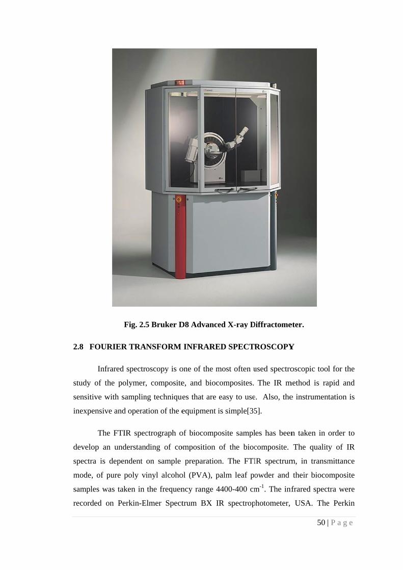
e Bruker D8
2
ength of inc
n is the orde
Fig. 2.4
of the film
perties of
ated from th
e by Scherre
0.89 to 1.3
used ( = 1.5
he Bragg’s a
study the X
fractometer
8 Advanced
cident X-ra
er of diffrac
4 Schemati
m co-relates
materials.
he full widt
er’s equatio
39, in prese
54056Å),
angle of the
X-ray diffrac
for 2=10
d X-ray Diff
ay, d is the
tion. Schem
ic view of X
s the depen
The crys
th at half m
n as follow
ent case we
is full wid
e X-ray diffr
ction has be
00 to 500 w
ffractometer
inter-plana
matic view o
XRD.
ndence of s
stallite size
maximum (FW
s [34]:
have taken
th in radian
raction peak
een carried o
with scannin
r is shown in
49
ar distance,
of XRD is s
structural, e
e of the p
WHM) of t
n K as 0.9.
ns at half m
k.
out with Br
ng rate of
n Fig. 2.5.
| P a g e
2.4
is the
shown in
electrical
polymer
the most
2.5
is the
maximum
ruker D8
0.20 per
2.8 FOUR
Infr
study of th
sensitive w
inexpensive
The
develop an
spectra is
mode, of p
samples wa
recorded o
Fig. 2.5
RIER TRA
rared spectr
he polymer
with samplin
e and opera
e FTIR spec
n understan
dependent
pure poly v
as taken in
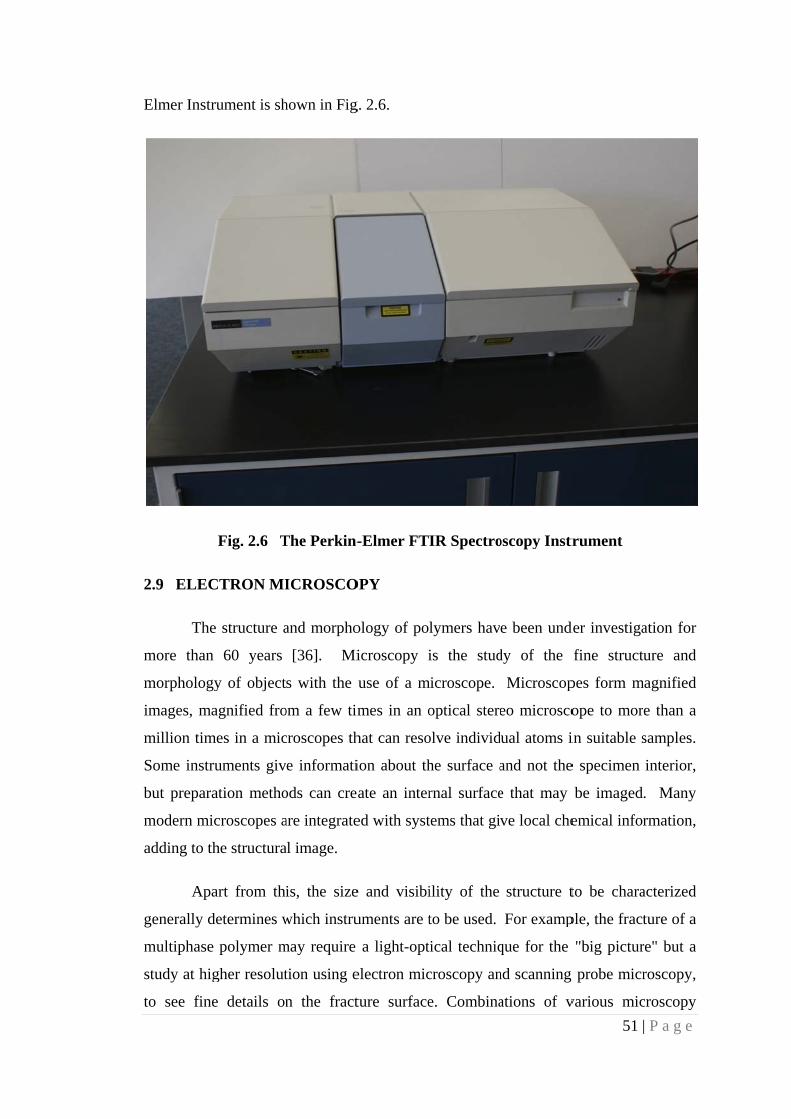
on Perkin-E
5 Bruker D
ANSFORM
oscopy is o
, composite
ng technique
ation of the e
ctrograph o
nding of co
on sample
inyl alcoho
the frequen
Elmer Spect
D8 Advance
INFRARE
one of the m
e, and bioc
es that are
equipment i
of biocompo
omposition
preparation
ol (PVA), p
ncy range 4
trum BX I
ed X-ray D
ED SPECTR
most often u
composites.
easy to use
is simple[35
osite sampl
of the bioc
n. The FTI
palm leaf po
4400-400 cm
R spectrop
Diffractome
ROSCOPY
used spectro
The IR m
e. Also, the
5].
les has been
composite.
IR spectrum
owder and
m-1. The inf
photometer,
50
eter.
Y
oscopic too
method is ra
e instrumen
n taken in
The qualit
m, in transm
their bioco
frared spect
USA. The
| P a g e
l for the
apid and
ntation is
order to
ty of IR
mittance
omposite
tra were
e Perkin
Elmer Instr
2.9 ELEC
The
more than
morphology
images, ma
million tim
Some instru
but prepara
modern mic
adding to th
Apa
generally d
multiphase
study at hig
to see fine
rument is sh
Fig. 2.6 T
CTRON MI
e structure a
60 years
y of object
agnified fro
mes in a mic
uments giv
ation metho
croscopes a
he structura
art from thi
determines w
polymer m
gher resolut
e details on
hown in Fig
The Perkin-
ICROSCO
and morpho
[36]. Mi
s with the
om a few tim
croscopes th
e informati
ods can cre
are integrate
al image.
is, the size
which instru
may require
tion using e
n the fract
g. 2.6.
-Elmer FT
OPY
ology of po
icroscopy i
use of a m
mes in an o
hat can reso
ion about th
ate an inter
ed with syst
e and visibi
uments are t
a light-opt
electron mic
ture surface
IR Spectro
lymers hav
is the stud
microscope.
optical stere
olve individ
he surface a
rnal surface
tems that gi
ility of the
to be used.
tical techniq
croscopy an
e. Combina
oscopy Instr
e been und
dy of the
Microscop
eo microsco
dual atoms i
and not the
e that may
ve local che
structure t
For examp
que for the
nd scanning
ations of v
51
rument
der investiga
fine struct
pes form m
ope to mor
in suitable s
e specimen
be imaged
emical infor
to be chara
ple, the fract
"big pictur
g probe micr
various mic
| P a g e
ation for
ure and
magnified
e than a
samples.
interior,
. Many
rmation,
acterized
ture of a
re" but a
roscopy,
croscopy

52 | P a g e
techniques generally provide the best insight into the morphology of polymer
materials [37].
In the present study the Scanning electron microscopy and atomic force
microscopy have been utilized to develop the understanding of surface structure of
biocomposite polymer. The brief descriptions of above microscopies are given in
following paragraphs.
2.9.1 Atomic Force Microscopy
Atomic force microscopy, also referred to as scanning force microscopy, is
obviously not a technique based on electron microscopy. However, it has been
widespread practiced in the last few years to supplement electron microscopy with
atomic force microscopy, as the latter enables the straightforward surface
characterization of polymers and provides supplementary insight into the structure
and properties of homopolymers, blends and composites [38]. The surface
topography of prepared biocomposite polymer samples was determined using an
Atomic Force Microscope (AFM) Nanoscope II from the Digital Instrument; in the
contact mode and analysis was carried out using software (Version 2.2) available with
the AFM at consortium for scientific research, Indore.
2.10 MICROHARDNESS MEASUREMENTS
The search for quantitative structure-property relationships for the control and
prediction of the mechanical behaviour of polymers and biocomposite has occupied a
central role in the development of polymer science and engineering. Mechanical
performance factors such as creep resistance, fatigue life, toughness and the stability
of properties with time, stress and temperature have become subjects of major
activity. Within this context microhardness emerges as a property which is sensitive
to structural changes.The most important hardness test has two variants: (i) the nature
of indenter, and (ii) the load applied.
The methods most widely used in determining the hardness of metals are the
static indentation methods. These involve the formation of a permanent indentation on
the surface of the material under examination, the hardness being determined by the
load and the size of the indentation formed.In the Brinell test [39] the indenter

53 | P a g e
consists of a hard steel ball, though in examining very hard metals the spherical
indenter may be made of tungsten carbide or even of diamond.Another type of
indenter which has been widely used is the conical or pyramidal indenter as used in
the Ludwik [40] and Vickers [41] hardness tests, respectively. These indenters are
now usually made of diamond. The hardness behaviour is different from that observed
with spherical indenters. In the present investigation, Vickers Diamond Pyramid
Indenter has been used for the determination of hardness. This method is, therefore,
discussed in detail in the following section.
2.10.1 Vicker's Test
Vicker's tester was introduced by Smith and Sandland in 1925. The test given
by them is an ideal method which can be used for research and laboratory work [41].
The advantage of the method is that it can be used for thin and superficially hardened
materials for which other methods are not suitable in comparison to this method.
Diamond in the form of square based pyramid, makes the Vickers indenter.
Like the Brinell test the (Fig. 2.9) hardness number is derived from the relationship
between the applied load and the surface area of the indentation. A pyramid has the
advantage that similar geometrical impressions are obtained at different applied loads.
As the ideal and most desirable ratio of indentation diameter to the ball
diameter in Brinell test was 0.375. Smith and Sandland chose 136° for the included
angle between diamond pyramid faces. Fig. 2.7 illustrates the most desirable ball
impression of 0.375 D. If the tangents are drawn at the point of contacts at the ends of
such an impression diameter, the included angle comes out to be 136°. Fig. 2.8 shows
the shape of such a diamond pyramid indenter.
In Vicker's test the indenter is pressed into the material under observation for a
specific period. The applied load may be 5 g to 160 g, which is selected according to
the thickness and the hardness of the specimen. When the applied load is removed the
impression produced is of the form as shown in Fig 2.8.

By
the resultin
often design
whe
means of m
ng impressi
nated as Hv
ere,
L = loa
d = Me
Fig. 2.7 B
Fig. 2.8 V
micrometer e
ion is meas
v which is gi
d in kilogra
an diagonal
(Ve
Ball Impress
Vicker’s Pyr
eye piece, t
sured. The
iven by
am.
l of the imp
ertical + Hor
sion for ide
ramidal In
the average
Diamond
ression in m
rizontal dia
eal ball
denter
length of th
Pyramid H
mm
gonal) / 2.
54
he two diag
Hardness nu
| P a g e
gonals of
umber is
2.6

55 | P a g e
= angle between the opposite faces of the diamond (136°).
Hence, the Vicker's hardness number,
H2LSin68
d
H.
2.7
In the present investigation specimens of biocomposite polymer, 1cm x 1 cm
in size prepared from the films were characterized with Carl-Zeiss Universal Research
Microscope NU-2. The universal research microscope NU–2 is a reflection type
microscope. It can also be used as a reflection phase contrast microscope, multiple
beam interference equipment and mhp – 160 microhardness tester. The same surface
can be observed in transmitted, incident and polarized light. The field of view can be
dark as well as in phase contrast. The important specification of the microhardness
tester is as below:
Model - Carl Zeiss NU-2 universal research microscope
Microhardness - mhp – 160 microhardness tester
Load Range - 5-160g
Light Source - Xenon lamp
Indenter - Vicker’s diamond pyramid indenter

Fig. 2.9 C
16
2.11 TENS
The
load carried
Universal T
data can be
The
specificatio
Carl Zeiss N
60 microha
SILE CHAR
e tensile tes
d by the spe
Testing Ma
e translated i
e tensile test
ons:
NU-2 univer
ardness test
RACTERI
ting is perf
ecimen. Thi
achine. Usin
into a stress
t was carrie
rsal resear
ter
IZATION
formed by e
is is done u
ng the spec
s strain curv
ed out with
rch microsc
elongating a
using a test
cimen dimen
ve [42].
Instron 336
cope attach
a specimen
machine kn
nsion, the l
69 (UTM). I
56
hed with mh
and measu
nown as the
load and de
It has the fo
| P a g e
hp –
uring the
e Instron
eflection
ollowing

Instron 33
Load cell c
Maximum
Speed rang
Height
Width
Depth
Fi
2.12 TH
In t
necessary e
current me
accurate m
voltage uni
were used a
69
apacity
force
ge
g. 2.10 Ins
ERMALLY
this section
equipments
easurement.
measuremen
it, Keithley
at various p
stron 3369-
Y STIMUL
we describ
used for ele
Sample ho
nt with eas
y electrome
laces depen
S
5
2
0
7
7
- Instrumen
LATED DI
be the detai
ectrical mea
older has b
se. Other i
eter (Type-6
nding upon
Specificatio
50 kN (112
25 kn (at m
0.005 to 500
1582 mm
756 mm
707 mm
nt for Tens
SCHARGE
ils of circui
asurements
been specia
instrument,
610C) and
the experim
on
50 lb)
aximum spe
0 mm/min
ile Charact
E CURREN
try, instrum
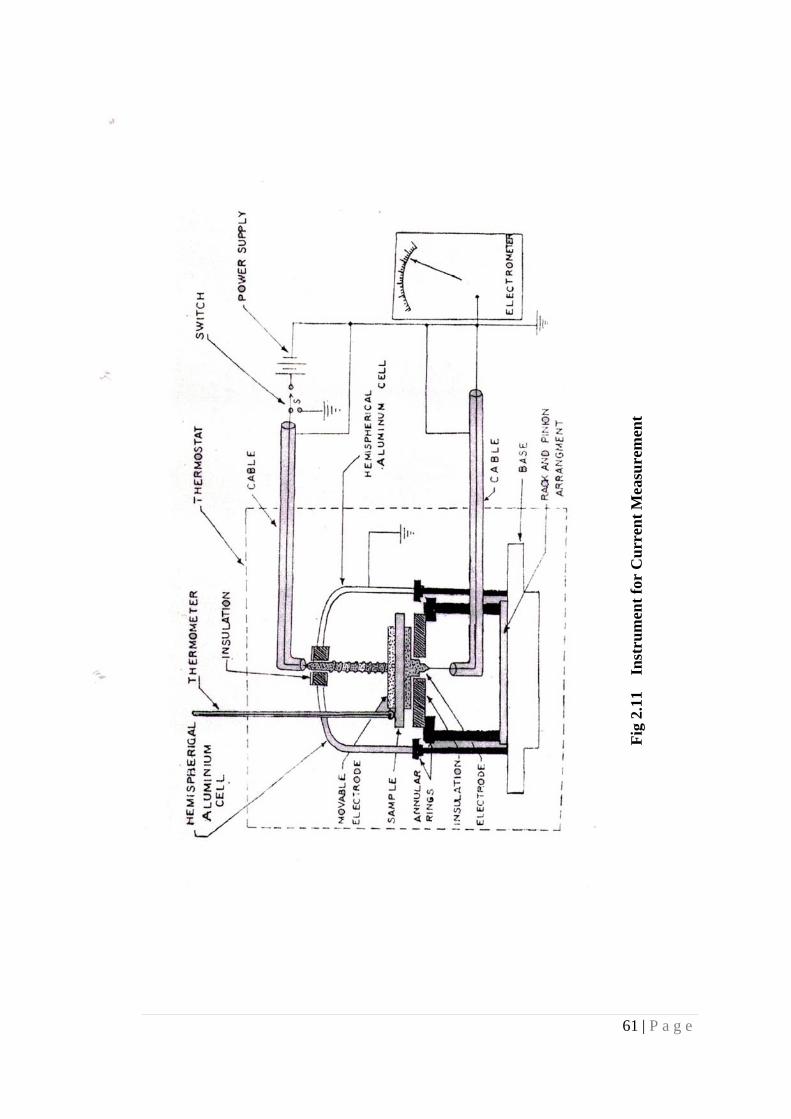
. Fig. 2.11 s
ally designe
e.g. electr
temperatur
mental requir
57
eed)
terisation.
NT
mentation an
shows the s
ed for carry
ric amplifie
re programm
irements.
| P a g e
nd other
setup for
ying out
er, high
mer etc.

58 | P a g e
2.12.1 Sample Holder Arrangement
To obtain reliable result in accurate measurement of current, the specimen
must be kept in the sample holder, which is dry, rigid and well shielded from spurious
current. A good sample holder has high insulation resistance, possesses freedom from
spurious voltage, induced charges, microphonics, and has no leakage of current.
Rigidity is required to avoid picking up of undesired induction.
In the present investigation, the insulators of high resistivity were used as test
specimen. In almost all the studies, high values of voltage and low values of currents
were involved. During the measurement of very low current produced due to high
voltage drop across a high resistance, insulation of the leads, fixture and voltmeter
must be several orders of magnitude greater than the resistance of the specimen. In the
absence of such insulation the current will start flowing through leads and other less
insulating parts. Keeping this in mind, best insulating material Teflon – FEP was used
wherever the insulation was required. Teflon-FEP has a very high volume resistivity
and a surface on which water/moisture film is not readily formed. Its insulation
properties remain unaffected by humidity of the air, perspiration and finger oil due to
normal manual handling. It is chemically inert to various organic solvents and can be
cleaned by many liquids and also can be machined in the desired shape. This is
possible because of its excellent mechanical and thermal properties. However, to
avoid surface conduction through the deposited dust, solid flux and oil or water film
on the surface, attention was constantly paid for keeping the insulation clean and dry.
Methyl alcohol or benzene was used for cleaning purpose.
Spurious voltage is always expected to affect the system performance in high
resistance circuits. This may be caused either due to internal electrical disturbances or
due to the internal induced signals. Line disturbances were avoided using highly
stabilized voltage to drive electrical instruments and the induced signals were avoided
using electrostatic shielding. To achieve this, all leads were surrounded by grounded
conducting surfaces and the high resistance circuit was enclosed in a shielded
aluminum enclosure inside the oven.
In any high resistance circuitry, physical motion of the system, may distort the
result in the following ways:
59 | P a g e
(a) If the coaxial cables are moved during the measurements, friction between the
braid and the insulator surrounding the central conductor or piezoelectric effect
in insulator may develop voltage across the electrometer input, thus distorting
the result. This can greatly be minimized by using “low noise cables” type RC
58 A/u. In these cables the surface under the shielded braid is coated with
graphite powder to provide a conducting equi-potential cylinder around the
insulator and conducting path for any charge that is generated.
(b) The movements of coaxial cables may also change the capacitance between the
shield and input lead, as a small charge is always present in this capacitance.
This change in capacitance ΔC may produce a voltage change ΔV, where,
ΔV = Q/ΔC 2.8
which should be seen by the electrometer. Rigid connection and firm
mechanical support to the flexible cables were found to be necessary to
minimise these effects.
2.12.2 Other Equipments Used
Important specifications of other equipments used during the electrical
investigations are given as:
(a) Electric amplifier
Model EA – 815
Manufacturer Electronic Corporation of India Limited Hyderabad.
Current range 10-5 to 10-14 amperes (full scale for both polarities )
Accuracy 3%
Voltage range 10 m V to 10 V (full scale for both polarities)
Input impedance More than 1014 ohms in open position of input impedance switch (voltage measurements)

60 | P a g e
(b) High voltage unit
Model Type 4800B
Manufacturer Electronic corporation of India Limited, Hyderabad.
Output voltage 50 to 3000 Volt (On both polarities).
(c) Keithley electrometer
Model Type 610C
Manufacturer Keithley Instruments, Inc. Cleveland. Ohio, USA
Range Current 10-14 to 0.3 amperes.
Accuracy +2% of full scale on 0.3 to 10-14 ampere ranges. + 4% of full scale on 10-12 to 10-4 ampere range.
Input impedance
More than 1014 ohms shunted by Pico farads (input impedance selectable in steps from 10 to 1011 ohms)
(d) Temperature programmer
Model Cole Parmer Model No.5C 6010 S.
Manufacturer Valley Forge Instruments Co.Inc. Phoenixville Pa.U.S.A.
Temperature range
0º to 400ºC
Rate of temperature rise
1º to 10º C/min. (adjustable).
61
Fig
2.1
1
Inst
rum
ent
for
Cu
rren
t M
easu
rem
ent
| P a g e
g

62 | P a g e
2.13 References:
[1] Braun Dietrich, CherdronHarald, Rehahn Matthias, Ritter H., Polymer
synthesis: theory and practice : fundamentals, methods, experiments, Springer
Berlin Heidelberg New York, 2005.
[2] KorotcenkovGhenadii, Chemical Sensors: Volume 1 General Approaches,
Momentum Press, New York, 2010.
[3] Glocker, D. A. and Shah, S. I. (Eds.), Handbook of Thin Film Process
Technology, Institute of Physics Publishing, Bristol and Philadelphia, 1998.
[4] L.P.Deshmukh, A.B.Palwe and V.S.Sawant, Sol. Energy Mater., 20, 337, 1990.
[5] Freund L. B., Suresh Subra, Thin Film Materials: Stress, Defect Formation, and
Surface Evolution, Cambridge University Press, U.K., 2003
[6] Mattox Donald M., Handbook of Physical Vapor Deposition (PVD) Processing,
Second Edition, Elsevier Inc, 2010.
[7] BunshahRointanFramroze, Handbook of Hard Coatings: Deposition
Technologies, Properties and Applications, Noyes Publication, Norwich, New
York, USA, 2001
[8] Popov, O. A., Physics of Thin Film Series, (Eds. M. H. Francombe and J.
Vossen), Vol. 18, pp. 122, Academic Press, 1991.
[9] Reif, R. and Kern, W., Thin Film Processes II, (Eds. J. L. Vossen and W. Kern),
Academic Press, 1991.
[10] Hey, H. P. W., Sluijk, B. G. and Hemmes, D. G., Solid State Tech., 33, 139,
1990.
[11] d’Agnostino, R. (Ed.), Plasma Deposition, Treatment and Etching of Polymers,
Academic Press, 1991.
[12] Felts, J. T. and Grubb, A. D., J. Vac. Sci. Tech, A10, 1675, 1992.
[13] Schwartz, M., Deposition from Aqueous Solutions: An overview. In: Handbook
of Deposition Technologies for Film and Coatings (Ed. R. F. Bunshah,), Noyes
Publications, 1994.

63 | P a g e
[14] Dinni, J. W., Electrodeposition: The Material Science of Coatings and
Substrates, Noyes Publications, 1993.
[15] Brewer, G. E. F. (Ed.), Electrodeposition of Coatings. In: Advances in
Chemistry, Series No. 119, American Chemical Society, 1973.
[16] Jonothan, J. and Berger, R., Plat. Surf. Finish, 80, 8, 1993.
[17] Koutsky, J. A. et al., J. Polym. Sci., 4, 661, 1966.
[18] Rastogi, A. C. and Chopra, K. L., Thin Solid Films, 18, 187, 1973.
[19] Khare, P. K. and Pal, A., J. Electrostat., 68, 328, 2010.
[20] Wagner, M. F., Thermochemic. Acta, 23, 93, 1978.
[21] Jain, K., Rastogi, A. C. and Chopra K. L., Phys. Stat. Sol. (a), 20, 167, 1973.
[22] Nakagawa, K. and Ishida, Y., J. Polym. Sci. Polym., Phys., 11, 1503, 1973.
[23] Gasso, J., Thin Solid Films, 21, 43, 1974.
[24] Benes, N. E., Spijksma, G., Verweij, H., Wormesster, H. and Poelsema, B.,
Materials, Interfaces, and Electrochemical Phenomena, 47, 1212, 2001.
[25] Wormeester, H., Benes, N. E., Spijksma, G. I., Verweij,H. and Poelsema, Thin
Solid Films, 455, 747, 2004.
[26] Campbell, D. S., Handbook of Thin Film Technology, (Eds. L. I. Maissel and R.
Galang), McGraw Hill, New York, 1970.
[27] Lakatos, A. I., J. Appl. Phys., 46, 1744, 1970.
[28] Tolansky, S., Multiple Beam Interferometry of Surface and Films, Oxford
University Press, UK, 1948.
[29] Kondratenko, M. L. and Malik, A. I., Instrumet. and Expt. Tech., 17, 855, 1974.
[30] Reucroff, P. J. and Takahasi, K., J. Non-Cryst. Solids, 1, 71, 1975.
[31] Lupu, A. and Baltog, J., J. Polym. Sci. Polym. Phys., 12, 2399, 1974.
[32] Davis, D. K., J. Appl. Phys. D, 2, 1533, 1969.
[33] Sibilia John P., A Guide to Materials Characterization and Chemical Analysis,
John Wiley & Sons, Inc., New York, USA, 1996.

64 | P a g e
[34] Cullity B.D., Elements of X-raf Diffraction, Second Edition, Addition Wesely,
London, 1978.
[35] Koenig, Jack L. Spectroscopy of polymers, Elsevier Science Inc., New York,
1999.
[36] MichlerGoerg H. Electron Microscopy of Polymers, Springer Berlin
Heidelberg, Germany, 2008.
[37] Sawyer Linda C., Grubb David T., Meyers Gregory F., Polymer Microscopy,
Third Edition, Spring, New York, USA, 2008.
[38] MichlerGoerg H., Electron Microscopy of Polymers, Springer-Verlag Berlin
Heidelberg, 2008
[39] Meyer, E., Z d. Vereines Deutsch. Ingenieure 52, 645, 1908.
[40] Ludwik, P., Die Kegelprobe, J. Springer, Berlin, 1908.
[41] Smith, R. &Sandland, G., J. Iron & Steel Inst. 1, 285, 1925.
[42] McKeen Laurence W., The effect of temperature and other factors on plastics
and elastomers,William Andrew, USA, 2007.


