2015-2017 Microchip Technology Inc. DS20005397C-page 1
Features
• Single Voltage Read and Write Operations
- 2.3-3.6V
• Serial Interface Architecture
- SPI Compatible: Mode 0 and Mode 3
• High Speed Clock Frequency
- 40MHz
• Dual Input/Output Support
- Fast-Read Dual-Output Instruction (3BH)- Fast-Read Dual I/O Instruction (BBH)
• Superior Reliability
- Endurance: 100,000 Cycles
- Greater than 20 years Data Retention
• Ultra-Low Power Consumption:
- Active Read Current: 5 mA (typical)- Standby Current: 5 µA (typical)
- Power-down Mode Standby Current: 3 µA (typical)
• Flexible Erase Capability
- Uniform 4 KByte sectors- Uniform 64 KByte overlay blocks
• Page Program Mode
- 256 Bytes/Page
• Fast Erase and Page-Program:
- Chip-Erase Time: 250 ms (typical)- Sector-Erase Time: 40 ms (typical)- Block-Erase Time: 80 ms (typical)- Page-Program Time: 4 ms/ 256 bytes
(typical)
• End-of-Write Detection
- Software polling the BUSY bit in Status Register
• Hold Pin (HOLD#)
- Suspend a serial sequence without deselecting the device
• Write Protection (WP#)
- Enables/Disables the Lock-Down function of the status register
• Software Write Protection
- Write protection through Block-Protection bits in status register
• Temperature Range
- Automotive AECQ-100 Grade 2 and Grade 3- Industrial: -40°C to +85°C- Extended: -40°C to +105°C
• Packages Available
- 8-contact USON (2 mm x 3 mm)- 8-lead SOIC (150 mils)- 8-contact WDFN (5mm x 6mm)
• All devices are RoHS compliant
Product Description
SST25PF040C is a member of the Serial Flash 25Series family and feature a four-wire, SPI-compatibleinterface that allows for a low pin-count package whichoccupies less board space and ultimately lowers totalsystem costs. SPI serial flash memory is manufacturedwith proprietary, high-performance CMOS SuperFlashtechnology. The split-gate cell design and thick-oxidetunneling injector attain better reliability and manufac-turability compared with alternate approaches.
This Serial Flash significantly improve performanceand reliability, while lowering power consumption. Thedevice writes (Program or Erase) with a single powersupply of 2.3-3.6V. The total energy consumed is afunction of the applied voltage, current, and time ofapplication. Since for any given voltage range, theSuperFlash technology uses less current to programand has a shorter erase time, the total energy con-sumed during any Erase or Program operation is lessthan alternative flash memory technologies.
SST25PF040C is offered in 8-lead SOIC and 8-contactWDFN and USON packages. See Figure 2-1 for the pinassignments.
SST25PF040C4 Mbit, 3.3V, SPI Serial Flash
SST25PF040C
DS20005397C-page 2 2015-2017 Microchip Technology Inc.
TO OUR VALUED CUSTOMERS
It is our intention to provide our valued customers with the best documentation possible to ensure successful use of your Microchipproducts. To this end, we will continue to improve our publications to better suit your needs. Our publications will be refined andenhanced as new volumes and updates are introduced.
If you have any questions or comments regarding this publication, please contact the Marketing Communications Department viaE-mail at [email protected]. We welcome your feedback.
Most Current Data Sheet
To obtain the most up-to-date version of this data sheet, please register at our Worldwide Web site at:
http://www.microchip.com
You can determine the version of a data sheet by examining its literature number found on the bottom outside corner of any page.The last character of the literature number is the version number, (e.g., DS30000000A is version A of document DS30000000).
Errata
An errata sheet, describing minor operational differences from the data sheet and recommended workarounds, may exist for currentdevices. As device/documentation issues become known to us, we will publish an errata sheet. The errata will specify the revisionof silicon and revision of document to which it applies.
To determine if an errata sheet exists for a particular device, please check with one of the following:
• Microchip’s Worldwide Web site; http://www.microchip.com• Your local Microchip sales office (see last page)When contacting a sales office, please specify which device, revision of silicon and data sheet (include literature number) you areusing.
Customer Notification System
Register on our web site at www.microchip.com to receive the most current information on all of our products.
SST25PF040C
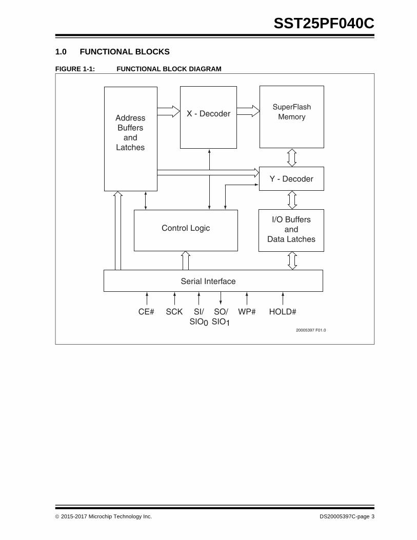
1.0 FUNCTIONAL BLOCKS
FIGURE 1-1: FUNCTIONAL BLOCK DIAGRAM
20005397 F01.0
I/O Buffersand
Data Latches
SuperFlashMemoryX - Decoder
Control Logic
AddressBuffers
andLatches
CE#
Y - Decoder
SCK SI/SIO0
SO/SIO1
WP# HOLD#
Serial Interface
2015-2017 Microchip Technology Inc. DS20005397C-page 3

SST25PF040C
2.0 PIN ASSIGNMENTS
FIGURE 2-1: PIN ASSIGNMENTS
8-Lead SOIC
8-Contact WDFN 5x6 mm
1
2
3
4
8
7
6
5
CE#
SO/SIO1
WP#
VSS
VDD
HOLD#
SCK
SI/SIO0
08-soic-P0.0
1
2
3
4
8
7
6
5
CE#
SO/SIO1
WP#
VSS
Top View
VDD
HOLD#
SCK
SI/SIO0
20005397 08-wson QA P1.0
8-Contact USON 2x3 mm
1
2
3
4
8
7
6
5
CE#
SO/SIO1
WP#
VSS
VDD
HOLD#
SCK
SI/SIO0
Top View
DS20005397C-page 4 2015-2017 Microchip Technology Inc.

SST25PF040C
TABLE 2-1: PIN DESCRIPTION
Symbol Pin Name Functions
SCK Serial Clock To provide the input/output timing of the serial interface.Commands, addresses, or input data are latched on the rising edge of the clock input, while output data is shifted out on the falling edge of the clock input.
SI Serial Data Input To transfer commands, addresses, or data serially into the device.Inputs are latched on the rising edge of the serial clock.
SO Serial Data Output To transfer data serially out of the device.Data is shifted out on the falling edge of the serial clock.
SIO[0:1] Serial Data Input/Output for Dual I/O Mode
To transfer commands, addresses, or data serially into the device, or data out of the device. Inputs are latched on the rising edge of the serial clock. Data is shifted out on the falling edge of the serial clock. These pins are used in Dual I/O mode
CE# Chip Enable The device is enabled by a high to low transition on CE#. CE# must remain low for the duration of any command sequence. The device is deselected and placed in Standby mode when CE# is high.
WP# Write Protect The Write Protect (WP#) pin is used to enable/disable BPL bit in the status reg-ister.
HOLD# Hold To temporarily stop serial communication with SPI Flash memory while device is selected.
VDD Power Supply To provide power supply voltage: 2.3-3.6V
VSS Ground
2015-2017 Microchip Technology Inc. DS20005397C-page 5
SST25PF040C
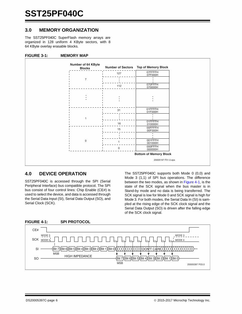
3.0 MEMORY ORGANIZATION
The SST25PF040C SuperFlash memory arrays areorganized in 128 uniform 4 KByte sectors, with 864 KByte overlay erasable blocks.
FIGURE 3-1: MEMORY MAP
4.0 DEVICE OPERATION
SST25PF040C is accessed through the SPI (SerialPeripheral Interface) bus compatible protocol. The SPIbus consist of four control lines: Chip Enable (CE#) isused to select the device, and data is accessed throughthe Serial Data Input (SI), Serial Data Output (SO), andSerial Clock (SCK).
The SST25PF040C supports both Mode 0 (0,0) andMode 3 (1,1) of SPI bus operations. The differencebetween the two modes, as shown in Figure 4-1, is thestate of the SCK signal when the bus master is inStand-by mode and no data is being transferred. TheSCK signal is low for Mode 0 and SCK signal is high forMode 3. For both modes, the Serial Data In (SI) is sam-pled at the rising edge of the SCK clock signal and theSerial Data Output (SO) is driven after the falling edgeof the SCK clock signal.
FIGURE 4-1: SPI PROTOCOL
20005197 F51.0.eps
Top of Memory Block
00FFFFH00F000H
000FFFH000000H
001FFFH001000H
Bottom of Memory Block. .
.
01FFFFH01F000H
01FFFFH010000H
. . .
. . .
07FFFFH07F000H
070FFFH070000H
. . .
Number of Sectors
15
0
1
. . .
31
16
. . .
. . .
127
112
. . .
1
0
. . .
7
Number of 64 KByteBlocks
20005397 F03.0
MODE 3
SCK
SI
SO
CE#
MODE 3
DON'T CARE
Bit 7 Bit 6 Bit 5 Bit 4 Bit 3 Bit 2 Bit 1 Bit 0
Bit 7 Bit 6 Bit 5 Bit 4 Bit 3 Bit 2 Bit 1 Bit 0
MODE 0MODE 0
HIGH IMPEDANCEMSB
MSB
DS20005397C-page 6 2015-2017 Microchip Technology Inc.

SST25PF040C
4.0.1 HOLD
In the hold mode, serial sequences underway with theSPI Flash memory are paused without resetting theclocking sequence. To activate the HOLD# mode, CE#must be in active low state. The HOLD# mode beginswhen the SCK active low state coincides with the fallingedge of the HOLD# signal. The Hold mode ends whenthe rising edge of the HOLD# signal coincides with theSCK active low state. HOLD# must not rise or fall whenSCK logic level is high. See Figure 4-2 for Hold Condi-tion waveform.
Once the device enters Hold mode, SO will be in high-impedance state while SI and SCK can be VIL or VIH.
If CE# is driven active high during a Hold condition, thedevice returns to standby mode. The device can thenbe re-initiated with the command sequences listed inTable 5-1. As long as HOLD# signal is low, the memoryremains in the Hold condition. To resume communica-tion with the device, HOLD# must be driven active high,and CE# must be driven active low. See Figure 4-2 forHold timing.
FIGURE 4-2: HOLD CONDITION WAVEFORM
4.1 Write Protection
SST25PF040C provides software Write protection. TheWrite Protect pin (WP#) enables or disables the lock-down function of the status register. The Block-Protec-tion bits (BP0, BP1, BP2, TB, and BPL) in the statusregister provide Write protection to the memory arrayand the status register. See Table 4-3 for the Block-Pro-tection description.
4.1.1 WRITE PROTECT PIN (WP#)
The Write Protect (WP#) pin enables the lock-downfunction of the BPL bit (bit 7) in the status register.When WP# is driven low, the execution of the Write-Status-Register (WRSR) instruction is determined bythe value of the BPL bit (see Table 4-1). When WP# ishigh, the lock-down function of the BPL bit is disabled.
Active Hold Active20005397 F05.0
SCK
HOLD#
TABLE 4-1: CONDITIONS TO EXECUTE WRITE-STATUS-REGISTER (WRSR) INSTRUCTION
WP# BPL Execute WRSR Instruction
L 1 Not Allowed
L 0 Allowed
H X Allowed
2015-2017 Microchip Technology Inc. DS20005397C-page 7
SST25PF040C
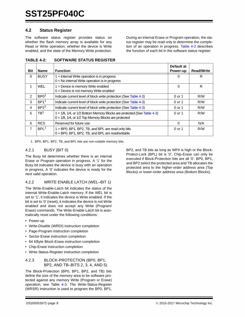
4.2 Status Register
The software status register provides status onwhether the flash memory array is available for anyRead or Write operation, whether the device is Writeenabled, and the state of the Memory Write protection.
During an internal Erase or Program operation, the sta-tus register may be read only to determine the comple-tion of an operation in progress. Table 4-2 describesthe function of each bit in the software status register.
4.2.1 BUSY (BIT 0)
The Busy bit determines whether there is an internalErase or Program operation in progress. A ‘1’ for theBusy bit indicates the device is busy with an operationin progress. A ‘0’ indicates the device is ready for thenext valid operation.
4.2.2 WRITE ENABLE LATCH (WEL–BIT 1)
The Write-Enable-Latch bit indicates the status of theinternal Write-Enable-Latch memory. If the WEL bit isset to ‘1’, it indicates the device is Write enabled. If thebit is set to ‘0’ (reset), it indicates the device is not Writeenabled and does not accept any Write (Program/Erase) commands. The Write-Enable-Latch bit is auto-matically reset under the following conditions:
• Power-up
• Write-Disable (WRDI) instruction completion
• Page-Program instruction completion
• Sector-Erase instruction completion
• 64 KByte Block-Erase instruction completion
• Chip-Erase instruction completion
• Write-Status-Register instruction completion
4.2.3 BLOCK-PROTECTION (BP0, BP1, BP2, AND TB–BITS 2, 3, 4, AND 5)
The Block-Protection (BP0, BP1, BP2, and TB) bitsdefine the size of the memory area to be software pro-tected against any memory Write (Program or Erase)operation, see Table 4-3. The Write-Status-Register(WRSR) instruction is used to program the BP0, BP1,
BP2, and TB bits as long as WP# is high or the Block-Protect-Lock (BPL) bit is ‘0’. Chip-Erase can only beexecuted if Block-Protection bits are all ‘0’. BP0, BP1,and BP2 select the protected area and TB allocates theprotected area to the higher-order address area (TopBlocks) or lower-order address area (Bottom Blocks).
TABLE 4-2: SOFTWARE STATUS REGISTER
Bit Name FunctionDefault atPower-up Read/Write
0 BUSY 1 = Internal Write operation is in progress0 = No internal Write operation is in progress
0 R
1 WEL 1 = Device is memory Write enabled0 = Device is not memory Write enabled
0 R
2 BP01
1. BP0, BP1, BP2, TB, and BPL bits are non-volatile memory bits.
Indicate current level of block write protection (See Table 4-3) 0 or 1 R/W
3 BP11 Indicate current level of block write protection (See Table 4-3) 0 or 1 R/W
4 BP21 Indicate current level of block write protection (See Table 4-3) 0 or 1 R/W
5 TB1 1 = 1/8, 1/4, or 1/2 Bottom Memory Blocks are protected (See Table 4-3)0 = 1/8, 1/4, or 1/2 Top Memory Blocks are protected
0 or 1 R/W
6 RES Reserved for future use 0 N/A
7 BPL1 1 = BP0, BP1, BP2, TB, and BPL are read-only bits0 = BP0, BP1, BP2, TB, and BPL are read/writable
0 or 1 R/W
DS20005397C-page 8 2015-2017 Microchip Technology Inc.

SST25PF040C
4.2.4 BLOCK PROTECTION LOCK-DOWN (BPL–BIT 7)
When the WP# pin is driven low (VIL), it enables theBlock-Protection-Lock-Down (BPL) bit. When BPL isset to ‘1’, it prevents any further alteration of the BP0,
BP1, BP2, TB, and BPL bits. When the WP# pin isdriven high (VIH), the BPL bit has no effect and its valueis ‘Don’t Care’.
TABLE 4-3: SOFTWARE STATUS REGISTER BLOCK PROTECTION
Protection Level
Status Register Bit
Protected Memory AddressTB BP2 BP1 BP0
0 (Full Memory Array unprotected) X 0 0 0 None
T1 (1/8 Top Memory Block protected) 0 0 0 1 070000H-07FFFFH
T2 (1/4 Top Memory Block protected) 0 0 1 0 060000H-07FFFFH
T3 (1/2 Top Memory Block protected) 0 0 1 1 040000H-07FFFFH
B1 (1/8 Bottom Memory Block protected) 1 0 0 1 000000H-00FFFFH
B2 (1/4 Bottom Memory Block protected) 1 0 1 0 000000H-01FFFFH
B3 (1/2 Bottom Memory Block protected) 1 0 1 1 000000H-03FFFFH
4 (Full Memory Block protected) X 1 X X 000000H-07FFFFH
2015-2017 Microchip Technology Inc. DS20005397C-page 9
SST25PF040C
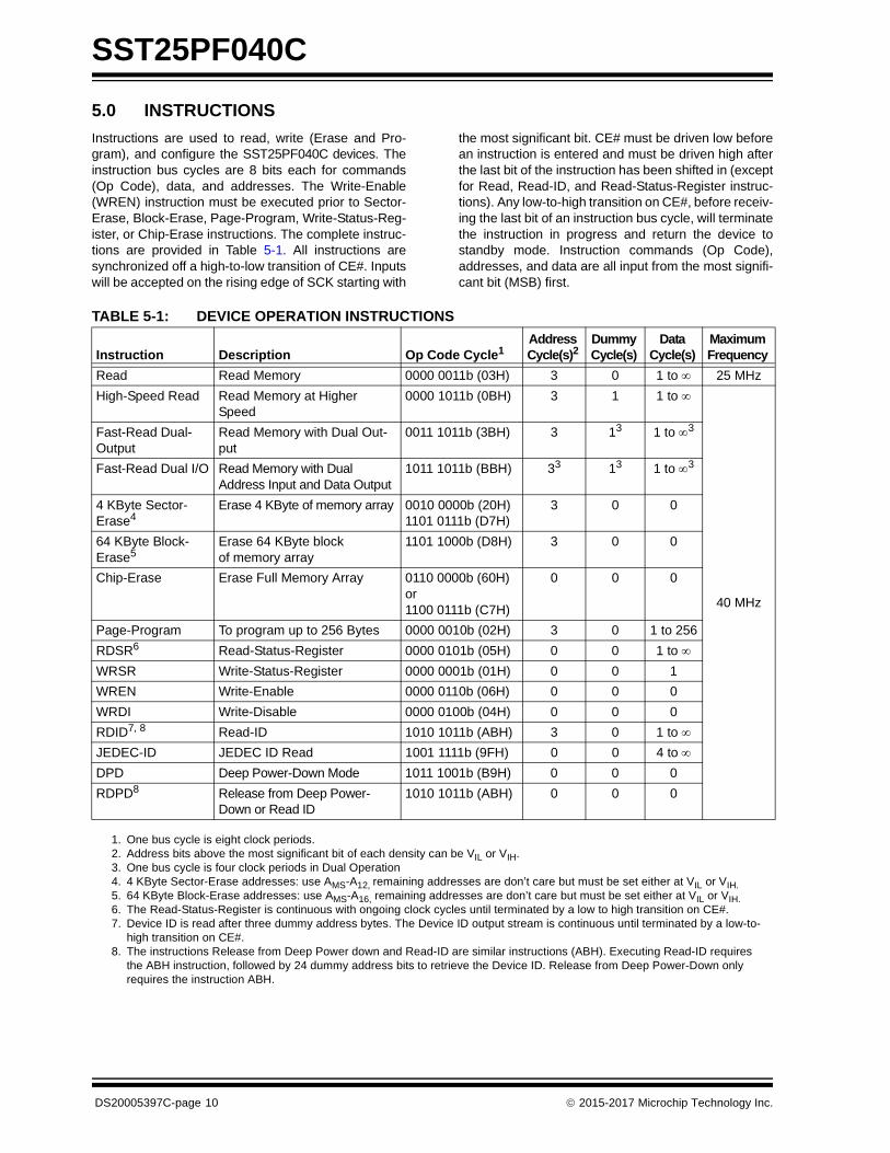
5.0 INSTRUCTIONS
Instructions are used to read, write (Erase and Pro-gram), and configure the SST25PF040C devices. Theinstruction bus cycles are 8 bits each for commands(Op Code), data, and addresses. The Write-Enable(WREN) instruction must be executed prior to Sector-Erase, Block-Erase, Page-Program, Write-Status-Reg-ister, or Chip-Erase instructions. The complete instruc-tions are provided in Table 5-1. All instructions aresynchronized off a high-to-low transition of CE#. Inputswill be accepted on the rising edge of SCK starting with
the most significant bit. CE# must be driven low beforean instruction is entered and must be driven high afterthe last bit of the instruction has been shifted in (exceptfor Read, Read-ID, and Read-Status-Register instruc-tions). Any low-to-high transition on CE#, before receiv-ing the last bit of an instruction bus cycle, will terminatethe instruction in progress and return the device tostandby mode. Instruction commands (Op Code),addresses, and data are all input from the most signifi-cant bit (MSB) first.
TABLE 5-1: DEVICE OPERATION INSTRUCTIONS
Instruction Description Op Code Cycle1
1. One bus cycle is eight clock periods.
Address Cycle(s)2
2. Address bits above the most significant bit of each density can be VIL or VIH.
Dummy Cycle(s)
DataCycle(s)
Maximum Frequency
Read Read Memory 0000 0011b (03H) 3 0 1 to 25 MHz
High-Speed Read Read Memory at Higher Speed
0000 1011b (0BH) 3 1 1 to
40 MHz
Fast-Read Dual-Output
Read Memory with Dual Out-put
0011 1011b (3BH) 3 13
3. One bus cycle is four clock periods in Dual Operation
1 to 3
Fast-Read Dual I/O Read Memory with Dual Address Input and Data Output
1011 1011b (BBH) 33 13 1 to 3
4 KByte Sector-Erase4
4. 4 KByte Sector-Erase addresses: use AMS-A12, remaining addresses are don’t care but must be set either at VIL or VIH.
Erase 4 KByte of memory array 0010 0000b (20H) 1101 0111b (D7H)
3 0 0
64 KByte Block-Erase5
5. 64 KByte Block-Erase addresses: use AMS-A16, remaining addresses are don’t care but must be set either at VIL or VIH.
Erase 64 KByte block of memory array
1101 1000b (D8H) 3 0 0
Chip-Erase Erase Full Memory Array 0110 0000b (60H) or 1100 0111b (C7H)
0 0 0
Page-Program To program up to 256 Bytes 0000 0010b (02H) 3 0 1 to 256
RDSR6
6. The Read-Status-Register is continuous with ongoing clock cycles until terminated by a low to high transition on CE#.
Read-Status-Register 0000 0101b (05H) 0 0 1 to
WRSR Write-Status-Register 0000 0001b (01H) 0 0 1
WREN Write-Enable 0000 0110b (06H) 0 0 0
WRDI Write-Disable 0000 0100b (04H) 0 0 0
RDID7, 8
7. Device ID is read after three dummy address bytes. The Device ID output stream is continuous until terminated by a low-to-high transition on CE#.
8. The instructions Release from Deep Power down and Read-ID are similar instructions (ABH). Executing Read-ID requires the ABH instruction, followed by 24 dummy address bits to retrieve the Device ID. Release from Deep Power-Down only requires the instruction ABH.
Read-ID 1010 1011b (ABH) 3 0 1 to
JEDEC-ID JEDEC ID Read 1001 1111b (9FH) 0 0 4 to
DPD Deep Power-Down Mode 1011 1001b (B9H) 0 0 0
RDPD8 Release from Deep Power-Down or Read ID
1010 1011b (ABH) 0 0 0
DS20005397C-page 10 2015-2017 Microchip Technology Inc.
SST25PF040C
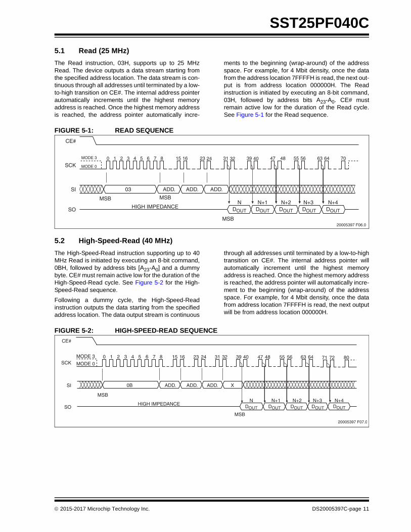
5.1 Read (25 MHz)
The Read instruction, 03H, supports up to 25 MHzRead. The device outputs a data stream starting fromthe specified address location. The data stream is con-tinuous through all addresses until terminated by a low-to-high transition on CE#. The internal address pointerautomatically increments until the highest memoryaddress is reached. Once the highest memory addressis reached, the address pointer automatically incre-
ments to the beginning (wrap-around) of the addressspace. For example, for 4 Mbit density, once the datafrom the address location 7FFFFH is read, the next out-put is from address location 000000H. The Readinstruction is initiated by executing an 8-bit command,03H, followed by address bits A23-A0. CE# mustremain active low for the duration of the Read cycle.See Figure 5-1 for the Read sequence.
FIGURE 5-1: READ SEQUENCE
5.2 High-Speed-Read (40 MHz)
The High-Speed-Read instruction supporting up to 40MHz Read is initiated by executing an 8-bit command,0BH, followed by address bits [A23-A0] and a dummybyte. CE# must remain active low for the duration of theHigh-Speed-Read cycle. See Figure 5-2 for the High-Speed-Read sequence.
Following a dummy cycle, the High-Speed-Readinstruction outputs the data starting from the specifiedaddress location. The data output stream is continuous
through all addresses until terminated by a low-to-hightransition on CE#. The internal address pointer willautomatically increment until the highest memoryaddress is reached. Once the highest memory addressis reached, the address pointer will automatically incre-ment to the beginning (wrap-around) of the addressspace. For example, for 4 Mbit density, once the datafrom address location 7FFFFH is read, the next outputwill be from address location 000000H.
FIGURE 5-2: HIGH-SPEED-READ SEQUENCE
20005397 F06.0
CE#
SO
SI
SCK
ADD.
0 1 2 3 4 5 6 7 8
ADD. ADD.03
HIGH IMPEDANCE
15 16 23 24 31 32 39 40 7047 48 55 56 63 64
N+2 N+3 N+4N N+1DOUT
MSB MSB
MSB
MODE 0
MODE 3
DOUT DOUT DOUT DOUT
20005397 F07.0
CE#
SO
SI
SCK
ADD.
0 1 2 3 4 5 6 7 8
ADD. ADD.0B
HIGH IMPEDANCE
15 16 23 24 31 32 39 40 47 48 55 56 63 64
N+2 N+3 N+4N N+1
X
MSB
MODE 0
MODE 3
DOUT DOUT DOUT DOUT
8071 72
DOUT
MSB
2015-2017 Microchip Technology Inc. DS20005397C-page 11

SST25PF040C
5.3 Fast-Read Dual Output (40 MHz)
The Fast-Read Dual-Output (3BH) instruction outputsdata up to 40 MHz from the SIO0 and SIO1 pins. To ini-tiate the instruction, execute an 8-bit command (3BH)followed by address bits A23-A0 and a dummy byte onSI/SIO0. Following a dummy cycle, the Fast-ReadDual-Output instruction outputs the data starting fromthe specified address location on the SIO1 and SIO0lines. SIO1 outputs, per clock sequence, odd data bitsD7, D5, D3, and D1; and SIO0 outputs even data bitsD6, D4, D2, and D0. CE# must remain active low for the
duration of the Fast-Read Dual-Output instructioncycle. See Figure 5-3 for the Fast-Read Dual-Outputsequence.
The data output stream is continuous through alladdresses until terminated by a low-to-high transitionon CE#. The internal address pointer will automaticallyincrement until the highest memory address isreached. Once the highest memory address isreached, the address pointer automatically incrementsto the beginning (wraparound) of the address space.For 4 Mbit density, once the data from address location7FFFFH has been read the next output will be fromaddress location 000000H.
FIGURE 5-3: FAST-READ DUAL OUTPUT SEQUENCE
20005397 F52.0
CE#
SIO1
SIO0
SCK0 1 2 3 4 5 6 7 8 28 29 30 31
MSB
MODE 3
MODE 0
32 33 34 35 36 37 38 39 40 41 42 43 44 45 46 47 48 49 50 51 52 53 54 55
6 4 2 0 6 4 2 0 6 4 2 0 6 4 2 0
7 5 3 1 7 5 3 1 7 5 3 1 7 5 3 1
24-Bit Address Dummy Cycle
DOUT
MSB
DOUT
MSB
DOUT
MSB
DOUT
3B
N N+1 N+2 N+3
IO, Switches from Input to Output
XADD. ADD. ADD.
15 16
HIGH IMPEDANCE
DS20005397C-page 12 2015-2017 Microchip Technology Inc.

SST25PF040C
5.4 Fast-Read Dual I/O (40 MHz)
The Fast-Read Dual I/O (BBH) instruction reduces thetotal number of input clock cycles, which results infaster data access. The device is first selected by driv-ing Chip Enable CE# low. Fast-Read Dual I/O is initi-ated by executing an 8-bit command (BBH) on SI/SIO0,thereafter, the device accepts address bits A23-A0 anda dummy byte on SI/SIO0 and SO/SIO1. It offers thecapability to input address bits A23-A0 at a rate of twobits per clock. Odd address bits A23 through A1 areinput on SIO1 and even address bits A22 through A0are input on SIO0, alternately For example, the mostsignificant bit is input first followed by A23/22, A21/A20,and so on. Each bit is latched at the same rising edgeof the Serial Clock (SCK). The input data during thedummy clocks is “don’t care”. However, the SIO0 andSIO1 pin must be in high-impedance prior to the fallingedge of the first data output clock.
Following a dummy cycle, the Fast-Read Dual I/Oinstruction outputs the data starting from the specifiedaddress location on the SIO1 and SIO0 lines. SIO1 out-puts, per clock sequence, odd data bits D7, D5, D3,and D1; and SIO0 outputs even data bits D6, D4, D2,and D0 per clock edge. CE# must remain active low forthe duration of the Fast-Read Dual I/O instructioncycle. The data output stream is continuous through alladdresses until terminated by a low-to-high transitionon CE#.
The internal address pointer will automatically incre-ment until the highest memory address is reached.Once the highest memory address is reached, theaddress pointer automatically increments to the begin-ning (wraparound) of the address space. For example,once the data from address location 7FFFFH is read,the next output is from address location 000000H. SeeFigure 5-4 for the Fast-Read Dual I/O sequence.
FIGURE 5-4: FAST-READ DUAL I/O SEQUENCE
20005397 F53.0
CE#
SIO1
SIO0
SCK0 1 2 3 4 5 6 7 8 9 10 11 12 13 14MODE 3
MODE 0
15 16 17 18 19 20 21 22 23 24 25 26 27 28 29 30 31 32 33 34 35 36 37 38
6 4 2 0 6 4 2 0 6 4 2 0
7 5 3 1 7 5 3 1 7 5 3 1
MSB
6 4 2 0 6 4 2 0 6 4 2 0 6 4 2 0
7 5 3 1 7 5 3 1 7 5 3 1 7 5 3 1
MSB MSB MSBA23-16 A15-8 A7-0
6
7
39
BB
DOUT DOUT DOUT DOUT
N N+1 N+2 N+3
IO, Switches from Input to Output
X
X
DummyCycle
2015-2017 Microchip Technology Inc. DS20005397C-page 13

SST25PF040C
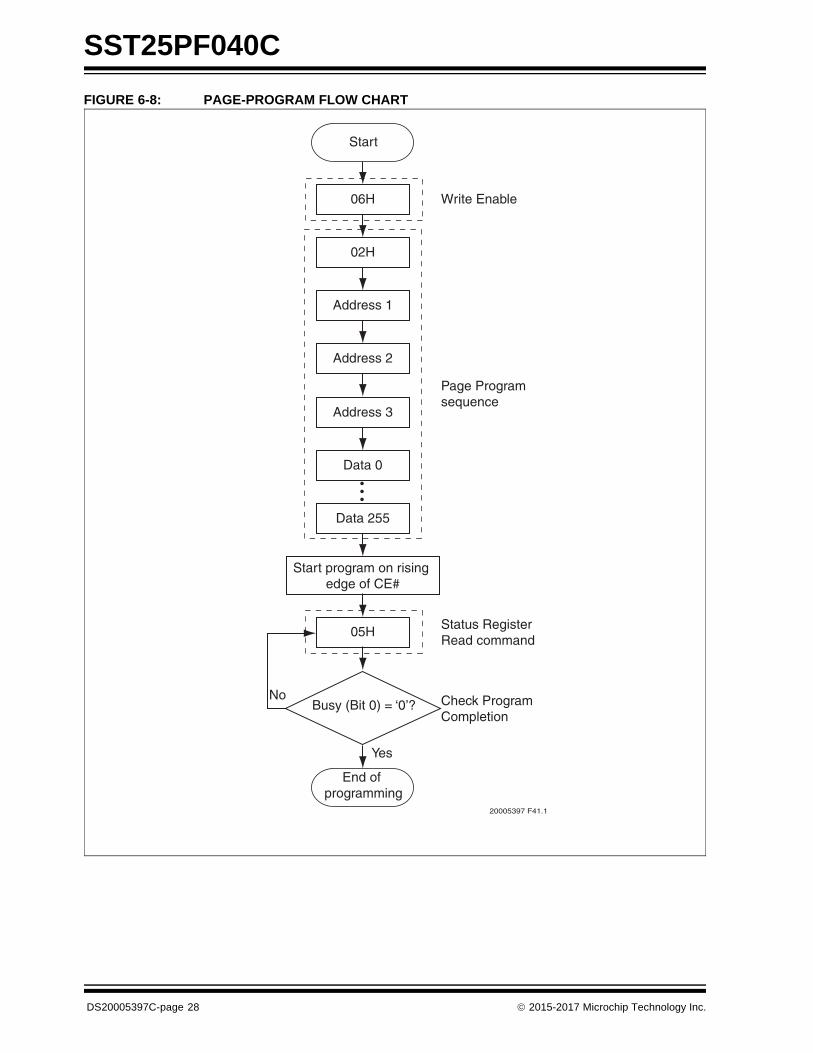
5.5 Page-Program
The Page-Program instruction programs up to 256Bytes of data in the memory. The data for the selectedpage address must be in the erased state (FFH) beforeinitiating the Page-Program operation. A Page-Pro-gram applied to a protected memory area will beignored. Prior to the program operation, execute theWREN instruction.
To execute a Page-Program operation, the host drivesCE# low, then sends the Page-Program commandcycle (02H), three address cycles, followed by the datato be programmed, and then drives CE# high. The pro-grammed data must be between 1 to 256 Bytes and inwhole byte increments; sending less than a full byte willcause the partial byte to be ignored. Poll the BUSY bitin the Status register, or wait TPP, for the completion of
the internal, self-timed, Page-Program operation. SeeFigure 5-5 for the Page-Program sequence and Figure6-8 for the Page-Program flow chart.
When executing Page-Program, the memory range forthe SST25PF040C is divided into 256-Byte pageboundaries. The device handles the shifting of morethan 256 Bytes of data by maintaining the last 256Bytes as the correct data to be programmed. If the tar-get address for the Page-Program instruction is not thebeginning of the page boundary (A[7:0] are not allzero), and the number of bytes of data input exceeds oroverlaps the end of the address of the page boundary,the excess data inputs wrap around and will be pro-grammed at the start of that target page.
FIGURE 5-5: PAGE-PROGRAM SEQUENCE
20005397 F60.1
CE#
SO
SI
SCK
ADD.
0 1 2 3 4 5 6 7 8
ADD. ADD. Data Byte 002
HIGH IMPEDANCE
15 16 23 24 31 32 39
MODE 0
MODE 3
MSBMSBMSB LSB
CE#(cont’)
SO(cont’)
SI(cont’)
SCK(cont’)
40 41 42 43 44 45 46 47 48
Data Byte 1
HIGH IMPEDANCE
MSBMSBMSB LSB
50 51 52 53 54 55 2072
49
Data Byte 2
2073
2074
2075
2076
2077
2078
2079
Data Byte 255
LSBLSB
LSB LSB
DS20005397C-page 14 2015-2017 Microchip Technology Inc.
SST25PF040C
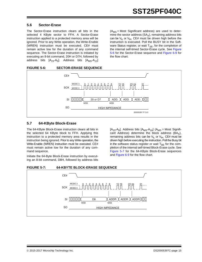
5.6 Sector-Erase
The Sector-Erase instruction clears all bits in theselected 4 KByte sector to FFH. A Sector-Eraseinstruction applied to a protected memory area will beignored. Prior to any Write operation, the Write-Enable(WREN) instruction must be executed. CE# mustremain active low for the duration of any commandsequence. The Sector-Erase instruction is initiated byexecuting an 8-bit command, 20H or D7H, followed byaddress bits [A23-A0]. Address bits [AMS-A12]
(AMS = Most Significant address) are used to deter-mine the sector address (SAX), remaining address bitscan be VIL or VIH. CE# must be driven high before theinstruction is executed. Poll the BUSY bit in the Soft-ware Status register, or wait TSE, for the completion ofthe internal self-timed Sector-Erase cycle. See Figure5-6 for the Sector-Erase sequence and Figure 6-9 forthe flow chart.
FIGURE 5-6: SECTOR-ERASE SEQUENCE
5.7 64-KByte Block-Erase
The 64-KByte Block-Erase instruction clears all bits inthe selected 64 KByte block to FFH. Applying thisinstruction to a protected memory area results in theinstruction being ignored. Prior to any Write operation, theWrite-Enable (WREN) instruction must be executed. CE#must remain active low for the duration of any com-mand sequence.
Initiate the 64-Byte Block-Erase instruction by execut-ing an 8-bit command, D8H, followed by address bits
[A23-A0]. Address bits [AMS-A16] (AMS = Most Signifi-cant Address) determine the block address (BAX),remaining address bits can be VIL or VIH. CE# must bedriven high before executing the instruction. Poll the Busy bitin the software status register or wait TBE for the com-pletion of the internal self-timed Block-Erase cycle. SeeFigure 5-7 for the 64-KByte Block-Erase sequencesand Figure 6-9 for the flow chart.
FIGURE 5-7: 64-KBYTE BLOCK-ERASE SEQUENCE
CE#
SO
SI
SCK
ADD.
0 1 2 3 4 5 6 7 8
ADD. ADD.20 or D7
HIGH IMPEDANCE
15 16 23 24 31
MODE 0
MODE 3
20005397 F13.0
MSBMSB
CE#
SO
SI
SCK
ADDR
0 1 2 3 4 5 6 7 8
ADDR ADDRD8
HIGH IMPEDANCE
15 16 23 24 31
MODE 0
MODE 3
MSB MSB
2015-2017 Microchip Technology Inc. DS20005397C-page 15
SST25PF040C
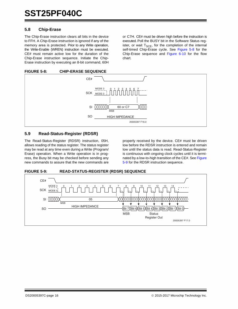
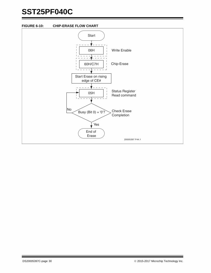
5.8 Chip-Erase
The Chip-Erase instruction clears all bits in the deviceto FFH. A Chip-Erase instruction is ignored if any of thememory area is protected. Prior to any Write operation,the Write-Enable (WREN) instruction must be executed.CE# must remain active low for the duration of theChip-Erase instruction sequence. Initiate the Chip-Erase instruction by executing an 8-bit command, 60H
or C7H. CE# must be driven high before the instruction isexecuted. Poll the BUSY bit in the Software Status reg-ister, or wait TSCE, for the completion of the internalself-timed Chip-Erase cycle. See Figure 5-8 for theChip-Erase sequence and Figure 6-10 for the flowchart.
FIGURE 5-8: CHIP-ERASE SEQUENCE
5.9 Read-Status-Register (RDSR)
The Read-Status-Register (RDSR) instruction, 05H,allows reading of the status register. The status registermay be read at any time even during a Write (Program/Erase) operation. When a Write operation is in prog-ress, the Busy bit may be checked before sending anynew commands to assure that the new commands are
properly received by the device. CE# must be drivenlow before the RDSR instruction is entered and remainlow until the status data is read. Read-Status-Registeris continuous with ongoing clock cycles until it is termi-nated by a low-to-high transition of the CE#. See Figure5-9 for the RDSR instruction sequence.
FIGURE 5-9: READ-STATUS-REGISTER (RDSR) SEQUENCE
CE#
SO
SI
SCK0 1 2 3 4 5 6 7
60 or C7
HIGH IMPEDANCE
MODE 0
MODE 3
20005397 F16.0
MSB
0 1 2 3 4 5 6 7 8 9 10 11 12 13 14
20005397 F17.0
MODE 3
SCK
SI
SO
CE#
Bit 7 Bit 6 Bit 5 Bit 4 Bit 3 Bit 2 Bit 1 Bit 0
05
MODE 0
HIGH IMPEDANCE
StatusRegister Out
MSB
MSB
DS20005397C-page 16 2015-2017 Microchip Technology Inc.
SST25PF040C
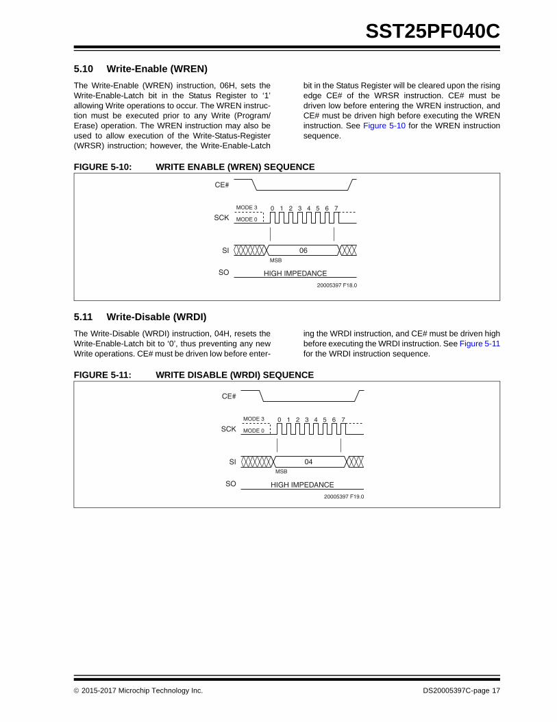
5.10 Write-Enable (WREN)
The Write-Enable (WREN) instruction, 06H, sets theWrite-Enable-Latch bit in the Status Register to ‘1’allowing Write operations to occur. The WREN instruc-tion must be executed prior to any Write (Program/Erase) operation. The WREN instruction may also beused to allow execution of the Write-Status-Register(WRSR) instruction; however, the Write-Enable-Latch
bit in the Status Register will be cleared upon the risingedge CE# of the WRSR instruction. CE# must bedriven low before entering the WREN instruction, andCE# must be driven high before executing the WRENinstruction. See Figure 5-10 for the WREN instructionsequence.
FIGURE 5-10: WRITE ENABLE (WREN) SEQUENCE
5.11 Write-Disable (WRDI)
The Write-Disable (WRDI) instruction, 04H, resets theWrite-Enable-Latch bit to ‘0’, thus preventing any newWrite operations. CE# must be driven low before enter-
ing the WRDI instruction, and CE# must be driven highbefore executing the WRDI instruction. See Figure 5-11for the WRDI instruction sequence.
FIGURE 5-11: WRITE DISABLE (WRDI) SEQUENCE
CE#
SO
SI
SCK0 1 2 3 4 5 6 7
06
HIGH IMPEDANCE
MODE 0
MODE 3
20005397 F18.0
MSB
CE#
SO
SI
SCK0 1 2 3 4 5 6 7
04
HIGH IMPEDANCE
MODE 0
MODE 3
20005397 F19.0
MSB
2015-2017 Microchip Technology Inc. DS20005397C-page 17
SST25PF040C
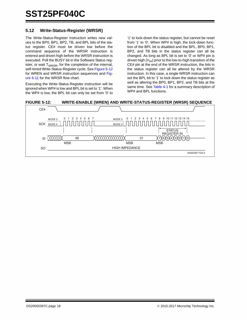
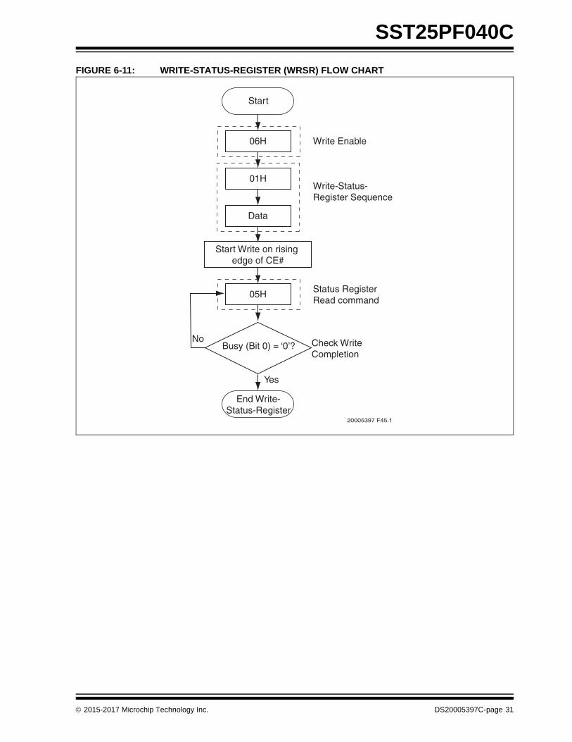
5.12 Write-Status-Register (WRSR)
The Write-Status-Register instruction writes new val-ues to the BP0, BP1, BP2, TB, and BPL bits of the sta-tus register. CE# must be driven low before thecommand sequence of the WRSR instruction isentered and driven high before the WRSR instruction isexecuted. Poll the BUSY bit in the Software Status reg-ister, or wait TWRSR, for the completion of the internal,self-timed Write-Status-Register cycle. See Figure 5-12for WREN and WRSR instruction sequences and Fig-ure 6-11 for the WRSR flow chart.
Executing the Write-Status-Register instruction will beignored when WP# is low and BPL bit is set to ‘1’. Whenthe WP# is low, the BPL bit can only be set from ‘0’ to
‘1’ to lock-down the status register, but cannot be resetfrom ‘1’ to ‘0’. When WP# is high, the lock-down func-tion of the BPL bit is disabled and the BPL, BP0, BP1,BP2, and TB bits in the status register can all bechanged. As long as BPL bit is set to ‘0’ or WP# pin isdriven high (VIH) prior to the low-to-high transition of theCE# pin at the end of the WRSR instruction, the bits inthe status register can all be altered by the WRSRinstruction. In this case, a single WRSR instruction canset the BPL bit to ‘1’ to lock down the status register aswell as altering the BP0, BP1, BP2, and TB bits at thesame time. See Table 4-1 for a summary description ofWP# and BPL functions.
FIGURE 5-12: WRITE-ENABLE (WREN) AND WRITE-STATUS-REGISTER (WRSR) SEQUENCE
20005397 F20.0
MODE 3
HIGH IMPEDANCE
MODE 0
STATUSREGISTER IN
7 6 5 4 3 2 1 0
MSBMSBMSB
01
MODE 3
SCK
SI
SO
CE#
MODE 0
06
0 1 2 3 4 5 6 7 0 1 2 3 4 5 6 7 8 9 10 11 12 13 14 15
DS20005397C-page 18 2015-2017 Microchip Technology Inc.
SST25PF040C
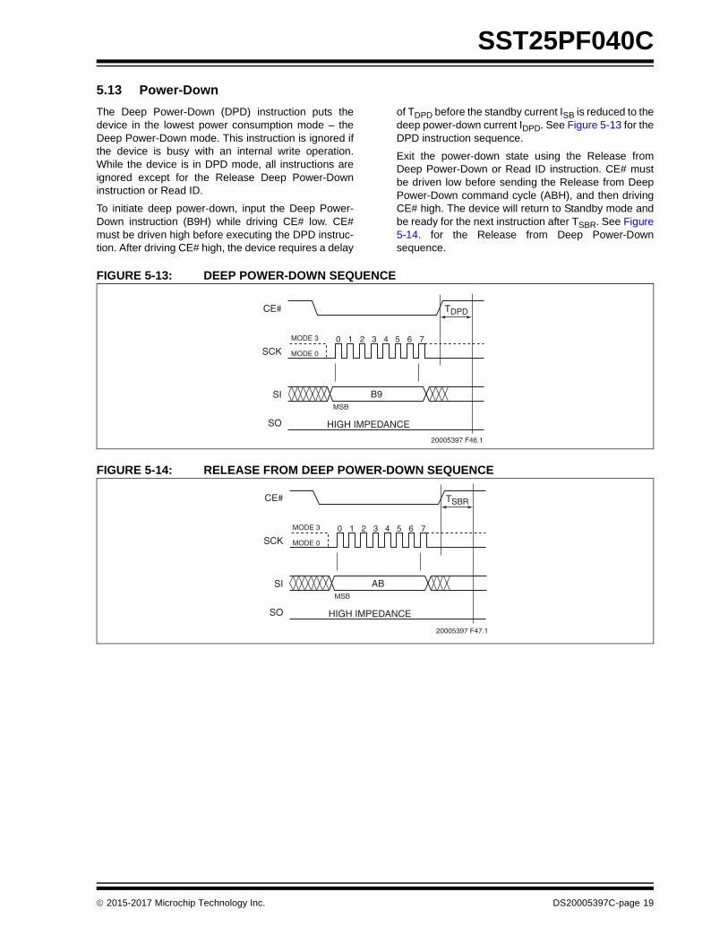
5.13 Power-Down
The Deep Power-Down (DPD) instruction puts thedevice in the lowest power consumption mode – theDeep Power-Down mode. This instruction is ignored ifthe device is busy with an internal write operation.While the device is in DPD mode, all instructions areignored except for the Release Deep Power-Downinstruction or Read ID.
To initiate deep power-down, input the Deep Power-Down instruction (B9H) while driving CE# low. CE#must be driven high before executing the DPD instruc-tion. After driving CE# high, the device requires a delay
of TDPD before the standby current ISB is reduced to thedeep power-down current IDPD. See Figure 5-13 for theDPD instruction sequence.
Exit the power-down state using the Release fromDeep Power-Down or Read ID instruction. CE# mustbe driven low before sending the Release from DeepPower-Down command cycle (ABH), and then drivingCE# high. The device will return to Standby mode andbe ready for the next instruction after TSBR. See Figure5-14. for the Release from Deep Power-Downsequence.
FIGURE 5-13: DEEP POWER-DOWN SEQUENCE
FIGURE 5-14: RELEASE FROM DEEP POWER-DOWN SEQUENCE
CE#
SO
SI
SCK0 1 2 3 4 5 6 7
B9
HIGH IMPEDANCE
MODE 0
MODE 3
20005397 F46.1
MSB
TDPD
CE#
SO
SI
SCK0 1 2 3 4 5 6 7
AB
HIGH IMPEDANCE
MODE 0
MODE 3
20005397 F47.1
MSB
TSBR
2015-2017 Microchip Technology Inc. DS20005397C-page 19
SST25PF040C
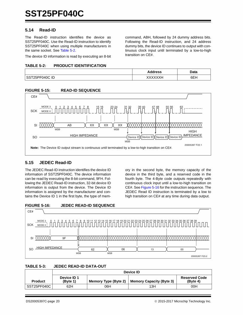
5.14 Read-ID
The Read-ID instruction identifies the device asSST25PF040C. Use the Read-ID instruction to identifySST25PF040C when using multiple manufacturers inthe same socket. See Table 5-2.
The device ID information is read by executing an 8-bit
command, ABH, followed by 24 dummy address bits.Following the Read-ID instruction, and 24 addressdummy bits, the device ID continues to output with con-tinuous clock input until terminated by a low-to-hightransition on CE#.
FIGURE 5-15: READ-ID SEQUENCE
5.15 JEDEC Read-ID
The JEDEC Read-ID instruction identifies the device IDinformation of SST25PF040C. The device informationcan be read by executing the 8-bit command, 9FH. Fol-lowing the JEDEC Read-ID instruction, 32-bit device IDinformation is output from the device. The Device IDinformation is assigned by the manufacturer and con-tains the Device ID 1 in the first byte, the type of mem-
ory in the second byte, the memory capacity of thedevice in the third byte, and a reserved code in thefourth byte. The 4-Byte code outputs repeatedly withcontinuous clock input until a low-to-high transition onCE#. See Figure 5-16 for the instruction sequence. TheJEDEC Read ID instruction is terminated by a low tohigh transition on CE# at any time during data output.
FIGURE 5-16: JEDEC READ-ID SEQUENCE
TABLE 5-2: PRODUCT IDENTIFICATION
Address Data
SST25PF040C ID XXXXXXH 6EH
20005397 F22.1
CE#
SO
SI
SCK
XX
0 1 2 3 4 5 6 7 8
XX XXAB
HIGH IMPEDANCE
15 16 23 24 31 32 39 40 47 48 55 56 63
Device ID Device ID
HIGHIMPEDANCE
MODE 3
MODE 0
MSB MSB
MSB
Device ID Device ID
Note: The Device ID output stream is continuous until terminated by a low-to-high transition on CE#.
TABLE 5-3: JEDEC READ-ID DATA-OUT
Product
Device ID
Device ID 1(Byte 1) Memory Type (Byte 2) Memory Capacity (Byte 3)
Reserved Code (Byte 4)
SST25PF040C 62H 06H 13H 00H
06 13 00
20005397 F23.2
CE#
SO
SI
SCK0 1 2 3 4 5 6 7 8
HIGH IMPEDANCE
15 1614 28 29 30 31
62
MODE 3
MODE 0
MSBMSB
9 10 11 12 13 17 18 32 34
9F
19 20 21 22 23 3324 25 26 27 37 38 3935 36
DS20005397C-page 20 2015-2017 Microchip Technology Inc.
SST25PF040C
6.0 ELECTRICAL SPECIFICATIONS
Absolute Maximum Stress Ratings (Applied conditions greater than those listed under “Absolute Maxi-mum Stress Ratings” may cause permanent damage to the device. This is a stress rating only and func-tional operation of the device at these conditions or conditions greater than those defined in the operationalsections of this data sheet is not implied. Exposure to absolute maximum stress rating conditions mayaffect device reliability.)
Temperature Under Bias . . . . . . . . . . . . . . . . . . . . . . . . . . . . . . . . . . . . . . . . . . . . . . . . . -55°C to +125°C
Storage Temperature . . . . . . . . . . . . . . . . . . . . . . . . . . . . . . . . . . . . . . . . . . . . . . . . . . . . -55°C to +150°C
D. C. Voltage on Any Pin to Ground Potential . . . . . . . . . . . . . . . . . . . . . . . . . . . . . . . .-0.5V to VDD+0.5V
Transient Voltage (<20 ns) on Any Pin to Ground Potential . . . . . . . . . . . . . . . . . . . . . . -2.0V to VDD+2.0V
Package Power Dissipation Capability (TA = 25°C) . . . . . . . . . . . . . . . . . . . . . . . . . . . . . . . . . . . . . . 1.0W
Surface Mount Solder Reflow Temperature . . . . . . . . . . . . . . . . . . . . . . . . . . . . . . . 260°C for 10 seconds
Output Short Circuit Current1 . . . . . . . . . . . . . . . . . . . . . . . . . . . . . . . . . . . . . . . . . . . . . . . . . . . . . . 50 mA
1. Output shorted for no more than one second. No more than one output shorted at a time.
TABLE 6-1: OPERATING RANGE
Range Ambient Temp VDD
Industrial -40°C to +85°C 2.3 - 3.6V
Extended -40°C to +105°C 2.3 - 3.6V
TABLE 6-2: AC CONDITIONS OF TEST
Input Rise/Fall Time Output Load
5ns CL = 30 pF
2015-2017 Microchip Technology Inc. DS20005397C-page 21
SST25PF040C
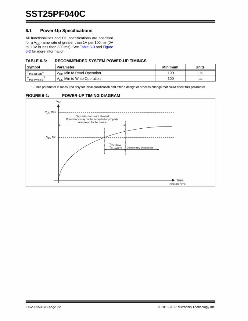
6.1 Power-Up Specifications
All functionalities and DC specifications are specifiedfor a VDD ramp rate of greater than 1V per 100 ms (0Vto 3.3V in less than 330 ms). See Table 6-3 and Figure6-2 for more information.
FIGURE 6-1: POWER-UP TIMING DIAGRAM
TABLE 6-3: RECOMMENDED SYSTEM POWER-UP TIMINGS
Symbol Parameter Minimum Units
TPU-READ1
1. This parameter is measured only for initial qualification and after a design or process change that could affect this parameter.
VDD Min to Read Operation 100 µs
TPU-WRITE1 VDD Min to Write Operation 100 µs
Time
VDD Min
VDD Max
VDD
Device fully accessibleTPU-READTPU-WRITE
Chip selection is not allowed.Commands may not be accepted or properly
interpreted by the device.
20005397 F27.0
DS20005397C-page 22 2015-2017 Microchip Technology Inc.

SST25PF040C
6.2 Hardware Data Protection
SST25PF040C provides a power-up reset function. Toensure that the power reset circuit will operate cor-rectly, the device must meet the conditions shown in
Figure 6-2 and Table 6-4. Microchip does not guaran-tee the data in the event of an instantaneous power fail-ure that occurs during a Write operation.
FIGURE 6-2: POWER-DOWN TIMING DIAGRAM
6.3 Software Data Protection
SST25PF040C prevents unintentional operations bynot recognizing commands under the following condi-tions:
• After inputting a Write command, if the rising CE# edge timing is not in a bus cycle (8 CLK units of SCK)
• When the Page-Program data is not in 1-byte increments
• If the Write Status Register instruction is input for two bus cycles or more.
6.4 Decoupling Capacitor
A 0.1µF ceramic capacitor must be provided for eachdevice and connected between VDD and VSS to ensurethat the device will operate correctly.
TABLE 6-4: RECOMMENDED SYSTEM POWER-DOWN TIMINGS
Symbol Parameter Min Max Units
TPD Power-down time 10 ms
VBOT Power-down voltage 0.2 V
TPD
VDD Min
VDD Max
VDD
20005397 F48.0
0V
VBOT
2015-2017 Microchip Technology Inc. DS20005397C-page 23
SST25PF040C
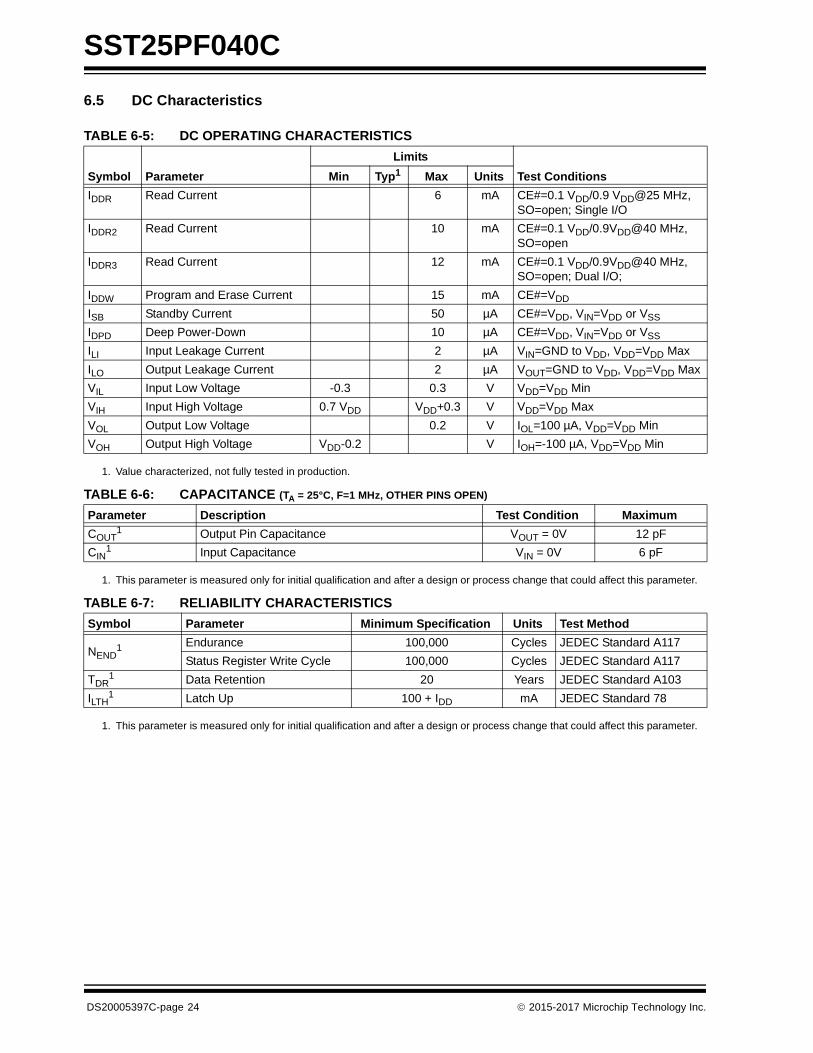
6.5 DC Characteristics
TABLE 6-5: DC OPERATING CHARACTERISTICS
Symbol Parameter
Limits
Test ConditionsMin Typ1
1. Value characterized, not fully tested in production.
Max Units
IDDR Read Current 6 mA CE#=0.1 VDD/0.9 VDD@25 MHz, SO=open; Single I/O
IDDR2 Read Current 10 mA CE#=0.1 VDD/0.9VDD@40 MHz, SO=open
IDDR3 Read Current 12 mA CE#=0.1 VDD/0.9VDD@40 MHz, SO=open; Dual I/O;
IDDW Program and Erase Current 15 mA CE#=VDD
ISB Standby Current 50 µA CE#=VDD, VIN=VDD or VSS
IDPD Deep Power-Down 10 µA CE#=VDD, VIN=VDD or VSS
ILI Input Leakage Current 2 µA VIN=GND to VDD, VDD=VDD Max
ILO Output Leakage Current 2 µA VOUT=GND to VDD, VDD=VDD Max
VIL Input Low Voltage -0.3 0.3 V VDD=VDD Min
VIH Input High Voltage 0.7 VDD VDD+0.3 V VDD=VDD Max
VOL Output Low Voltage 0.2 V IOL=100 µA, VDD=VDD Min
VOH Output High Voltage VDD-0.2 V IOH=-100 µA, VDD=VDD Min
TABLE 6-6: CAPACITANCE (TA = 25°C, F=1 MHz, OTHER PINS OPEN)
Parameter Description Test Condition Maximum
COUT1
1. This parameter is measured only for initial qualification and after a design or process change that could affect this parameter.
Output Pin Capacitance VOUT = 0V 12 pF
CIN1 Input Capacitance VIN = 0V 6 pF
TABLE 6-7: RELIABILITY CHARACTERISTICS
Symbol Parameter Minimum Specification Units Test Method
NEND1
1. This parameter is measured only for initial qualification and after a design or process change that could affect this parameter.
Endurance 100,000 Cycles JEDEC Standard A117
Status Register Write Cycle 100,000 Cycles JEDEC Standard A117
TDR1 Data Retention 20 Years JEDEC Standard A103
ILTH1 Latch Up 100 + IDD mA JEDEC Standard 78
DS20005397C-page 24 2015-2017 Microchip Technology Inc.

SST25PF040C
6.6 AC Characteristics
TABLE 6-8: AC OPERATING CHARACTERISTICS
Symbol ParameterLimits - 25 MHz Limits - 40 MHz
UnitsMin Max Min Max
FCLK1
1. Maximum clock frequency for Read instruction, 03H, is 25 MHz
Serial Clock Frequency 25 40 MHz
TSCKH Serial Clock High Time 18 11.5 ns
TSCKL Serial Clock Low Time 18 11.5 ns
TSCKR Serial Clock Rise Time 5 5 ns
TSCKF Serial Clock Fall Time 5 5 ns
TCES2
2. Relative to SCK
CE# Active Setup Time 8 8 ns
TCEH2 CE# Active Hold Time 8 8 ns
TCHS2 CE# Not Active Setup Time 8 8 ns
TCHH2 CE# Not Active Hold Time 8 8 ns
TCPH CE# High Time 25 25 ns
TCHZ CE# High to High-Z Output 8 8 ns
TCLZ SCK Low to Low-Z Output 0 0 ns
TDS Data In Setup Time 2 2 ns
TDH Data In Hold Time 5 5 ns
THLS HOLD# Low Setup Time 5 5 ns
THHS HOLD# High Setup Time 5 5 ns
THLH HOLD# Low Hold Time 5 5 ns
THHH HOLD# High Hold Time 5 5 ns
THZ HOLD# Low to High-Z Output 9 9 ns
TLZ HOLD# High to Low-Z Output 9 9 ns
TOH Output Hold from SCK Change 1 1 ns
TV Output Valid from SCK 11 11 ns
TWPS WP# Setup Time 20 20 ns
TWPH WP# Hold Time 20 20 ns
TWRSR Status Register Write Time 10 15 ms
TDPD CE# High to Deep Power-Down 3 3 µs
TSBRDeep Power-Down (CE# High) to Standby Mode
3 3 µs
TSE Sector-Erase 40 150 40 150 ms
TBE Block-Erase 80 250 80 250 ms
TCE Chip-Erase 0.25 2 0.25 2 s
TPP Page-Program (256 Byte) 4 5 4 5 ms
2015-2017 Microchip Technology Inc. DS20005397C-page 25

SST25PF040C
FIGURE 6-3: SERIAL OUTPUT TIMING DIAGRAM
FIGURE 6-4: SERIAL INPUT TIMING DIAGRAM
FIGURE 6-5: HOLD TIMING DIAGRAM
HIGH-Z HIGH-Z
CE#
SO
SI
SCK
MSB LSB
TDS TDH
TCHHTCES
TCEHTCHS
TSCKRTSCKF
TCPH
20005397 F24.0
20005397 F25.0
CE#
SI
SO
SCK
MSB
TCLZ
TV
TSCKH
TCHZTOH
TSCKL
LSB
THZ TLZ
THHH THLS
THLH
THHS
20005397 F26.1
HOLD#
CE#
SCK
SO
SI
THLH
DS20005397C-page 26 2015-2017 Microchip Technology Inc.

SST25PF040C
FIGURE 6-6: STATUS REGISTER WRITE TIMING
FIGURE 6-7: AC INPUT/OUTPUT REFERENCE WAVEFORMS
20005397 F49.0
TWPSTWPH
CE#
WP#
20005397 F28.0
REFERENCE POINTS OUTPUTINPUT
VHT
VLT
VHT
VLT
VIHT
VILT
AC test inputs are driven at VIHT (0.9VDD) for a logic ‘1’ and VILT (0.1VDD) for a logic ‘0’. Measurement referencepoints for inputs and outputs are VHT (0.5VDD) and VLT (0.5VDD). Input rise and fall times (10% 90%) are <5ns.
Note: VHT - VHIGH TestVLT - VLOW TestVIHT - VINPUT HIGH TestVILT - VINPUT LOW Test
2015-2017 Microchip Technology Inc. DS20005397C-page 27
SST25PF040C
FIGURE 6-8: PAGE-PROGRAM FLOW CHART
20005397 F41.1
06H
Yes
No
Start
02H
Address 1
Address 2
Address 3
Data 0
Data 255
05H
Start program on rising edge of CE#
Busy (Bit 0) = ‘0’?
End of programming
Write Enable
Page Programsequence
Status RegisterRead command
Check ProgramCompletion
•••
DS20005397C-page 28 2015-2017 Microchip Technology Inc.

SST25PF040C
FIGURE 6-9: SECTOR-ERASE OR 64-KBYTE BLOCK-ERASE FLOW CHART
20005397 F42.1
06H
Yes
No
Start
20H/D7 or D8H
Address 1
Address 2
Address 3
05H
Start Erase on rising edge of CE#
Busy (Bit 0) = ‘0’?
End of Erase
Write Enable
Sector-Erase (20H/D7H) or64-KByte Block-Erase (D8H) sequence
Status RegisterRead command
Check EraseCompletion
2015-2017 Microchip Technology Inc. DS20005397C-page 29
SST25PF040C
FIGURE 6-10: CHIP-ERASE FLOW CHART
20005397 F44.1
06H
Yes
No
Start
60H/C7H
05H
Start Erase on rising edge of CE#
Busy (Bit 0) = ‘0’?
End of Erase
Write Enable
Chip-Erase
Status RegisterRead command
Check EraseCompletion
DS20005397C-page 30 2015-2017 Microchip Technology Inc.
SST25PF040C
FIGURE 6-11: WRITE-STATUS-REGISTER (WRSR) FLOW CHART
20005397 F45.1
06H
Yes
No
Start
01H
Data
05H
Start Write on rising edge of CE#
Busy (Bit 0) = ‘0’?
End Write-Status-Register
Write Enable
Write-Status-Register Sequence
Status RegisterRead command
Check WriteCompletion
2015-2017 Microchip Technology Inc. DS20005397C-page 31
SST25PF040C
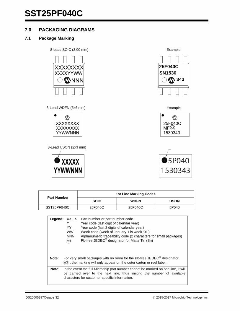
7.0 PACKAGING DIAGRAMS
7.1 Package Marking
Legend: XX...X Part number or part number codeY Year code (last digit of calendar year)YY Year code (last 2 digits of calendar year)WW Week code (week of January 1 is week ‘01’)NNN Alphanumeric traceability code (2 characters for small packages)
Pb-free JEDEC® designator for Matte Tin (Sn)
Note: For very small packages with no room for the Pb-free JEDEC® designator , the marking will only appear on the outer carton or reel label.
Note: In the event the full Microchip part number cannot be marked on one line, it willbe carried over to the next line, thus limiting the number of availablecharacters for customer-specific information.
3e
3e
Part Number1st Line Marking Codes
SOIC WDFN USON
SST25PF040C 25F040C 25F040C 5P040
8-Lead SOIC (3.90 mm) Example
NNN
25F040CSN1530
343
XXXXXXXXYYWWNNN
XXXXXXXXMF1530343
25F040Ce3
8-Lead WDFN (5x6 mm) Example
8-Lead USON (2x3 mm)
DS20005397C-page 32 2015-2017 Microchip Technology Inc.

SST25PF040C
Note: For the most current package drawings, please see the Microchip Packaging Specification located at http://www.microchip.com/packaging
2015-2017 Microchip Technology Inc. DS20005397C-page 33
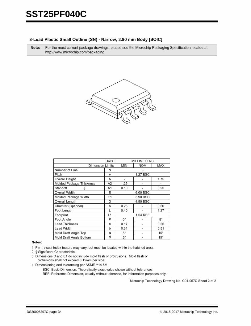
SST25PF040C
Note: For the most current package drawings, please see the Microchip Packaging Specification located at http://www.microchip.com/packaging
DS20005397C-page 34 2015-2017 Microchip Technology Inc.

SST25PF040C
���������� ��������� �������������������������� ��!�"��#$%
����& ������!"���#�������$����%�&���"'�����"��"���������������(��$�����������)������������%��������*++&&&�!��������!+���$�����
2015-2017 Microchip Technology Inc. DS20005397C-page 35

SST25PF040C
BA
0.15 C
0.15 C
D2
E2
8 X b0.10 C A B0.05 C
(DATUM B)
(DATUM A)
CSEATING
PLANE
NOTE 1
2X
BOTTOM VIEW
Microchip Technology Drawing C04-210B Sheet 1 of 2
For the most current package drawings, please see the Microchip Packaging Specification located athttp://www.microchip.com/packaging
Note:
N
0.10 C A B
0.10 C A B
A3
0.10 C
0.08 C
A1
D
E
NOTE 1
2X
A
1 2
1 2
e
SEE DETAIL A
SIDE VIEW
TOP VIEW
N
K
8-Lead Plastic Very, Very Thin Small Outline No-Lead (MF) - 5x6 mm Body [WDFN]
DS20005397C-page 36 2015-2017 Microchip Technology Inc.
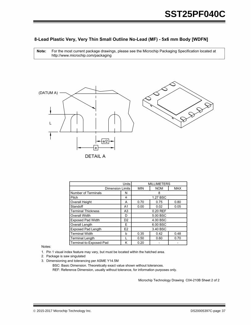
SST25PF040C
Microchip Technology Drawing C04-210B Sheet 2 of 2
For the most current package drawings, please see the Microchip Packaging Specification located athttp://www.microchip.com/packaging
Note:
e/2
e
L
(DATUM A)
DETAIL A
8-Lead Plastic Very, Very Thin Small Outline No-Lead (MF) - 5x6 mm Body [WDFN]
Number of Terminals
Overall Height
Terminal Width
Overall Width
Overall Length
Terminal Length
Exposed Pad Width
Exposed Pad Length
Terminal Thickness
Pitch
Standoff
UnitsDimension Limits
A1A
b
ED2
E2
A3
e
L
D
N1.27 BSC
0.20 REF
0.500.35
0.700.00
0.42
6.00 BSC
0.60
3.40 BSC
4.00 BSC
0.750.02
5.00 BSC
MILLIMETERSMIN NOM
8
0.700.48
0.800.05
MAX
K -0.20 -
REF: Reference Dimension, usually without tolerance, for information purposes only.BSC: Basic Dimension. Theoretically exact value shown without tolerances.
1.2.3.
Notes:
Pin 1 visual index feature may vary, but must be located within the hatched area.Package is saw singulatedDimensioning and tolerancing per ASME Y14.5M
Terminal-to-Exposed-Pad
2015-2017 Microchip Technology Inc. DS20005397C-page 37
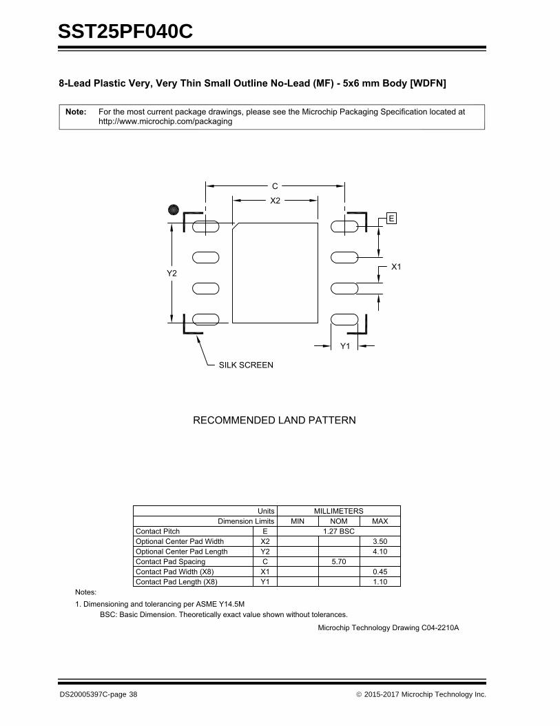
SST25PF040C
RECOMMENDED LAND PATTERN
For the most current package drawings, please see the Microchip Packaging Specification located athttp://www.microchip.com/packaging
Note:
Y2
SILK SCREEN
Y1
C
X2
X1
Dimension LimitsUnits
C
Optional Center Pad Width
Contact Pad SpacingOptional Center Pad Length
Contact Pitch
Y2X2
4.103.50
MILLIMETERS
1.27 BSCMIN
EMAX
5.70
Contact Pad Length (X8)Contact Pad Width (X8)
Y1X1
1.100.45
BSC: Basic Dimension. Theoretically exact value shown without tolerances.
Notes:1. Dimensioning and tolerancing per ASME Y14.5M
Microchip Technology Drawing C04-2210A
NOM
8-Lead Plastic Very, Very Thin Small Outline No-Lead (MF) - 5x6 mm Body [WDFN]
E
DS20005397C-page 38 2015-2017 Microchip Technology Inc.

SST25PF040C
BA
0.20 C
0.20 C
D
D2
E2
E
8 X b0.10 C A B0.05 C
(DATUM B)
(DATUM A)
CSEATING
PLANE
NOTE 1
2X
TOP VIEW
SIDE VIEW
BOTTOM VIEW
Microchip Technology Drawing C04-203C [PRX] Sheet 1 of 2
For the most current package drawings, please see the Microchip Packaging Specification located athttp://www.microchip.com/packaging
Note:
NOTE 1
0.10 C A B
0.10 C A B
0.10 C
0.08 C
A1A
e
SEE DETAIL A
1 2
N
1 2
N
2X
8-Lead Plastic Ultra Thin Small Outline No Lead Package (PRX) - 2x3 mm Body [USON][Also called UDFN]
2015-2017 Microchip Technology Inc. DS20005397C-page 39

SST25PF040C
Microchip Technology Drawing C04-203C [PRX] Sheet 2 of 2
For the most current package drawings, please see the Microchip Packaging Specification located athttp://www.microchip.com/packaging
Note:
L
(DATUM A)
e
e/2
L3
DETAIL A
L1
REF: Reference Dimension, usually without tolerance, for information purposes only.BSC: Basic Dimension. Theoretically exact value shown without tolerances.
1.2.3.
Notes:
Pin 1 visual index feature may vary, but must be located within the hatched area.Package is saw singulatedDimensioning and tolerancing per ASME Y14.5M
Number of Terminals
Overall Height
Terminal Width
Overall Width
Overall Length
Package Edge to Terminal Edge
Exposed Pad Width
Exposed Pad Length
Terminal Length
Pitch
Standoff
UnitsDimension Limits
A1A
b
ED2
E2
L3
e
L
D
N0.50 BSC
0.35
1.50
0.10
0.400.20
0.450.00
0.25
3.00 BSC
0.45
0.20
1.60
0.550.02
2.00 BSC
MILLIMETERSMIN NOM
8
1.70
0.30
0.500.30
0.600.05
MAX
0.30 0.40Package Edge to Terminal Edge L1 — 0.10 —
8-Lead Plastic Ultra Thin Small Outline No Lead Package (PRX) - 2x3 mm Body [USON][Also called UDFN]
DS20005397C-page 40 2015-2017 Microchip Technology Inc.

SST25PF040C
RECOMMENDED LAND PATTERN
For the most current package drawings, please see the Microchip Packaging Specification located athttp://www.microchip.com/packaging
Note:
Y2
SILK SCREEN
Y1
C
X2
X1
Dimension LimitsUnits
C
Optional Center Pad Width
Terminal Pad SpacingOptional Center Pad Length
Terminal Pitch
Y2X2
1.700.30
MILLIMETERS
0.50 BSCMIN
EMAX
2.80
Terminal Pad Length (X8)Terminal Pad Width (X8)
Y1X1
0.900.30
BSC: Basic Dimension. Theoretically exact value shown without tolerances.
Notes:1. Dimensioning and tolerancing per ASME Y14.5M
Microchip Technology Drawing C04-2203B [PRX]
NOM
E
G
Mininum Between Terminal Pads G 0.20
8-Lead Plastic Ultra Thin Small Outline No Lead Package (PRX) - 2x3 mm Body [USON][Also called UDFN]
2015-2017 Microchip Technology Inc. DS20005397C-page 41

SST25PF040C
TABLE 7-1: REVISION HISTORY
Revision Description Date
A • Initial release of data sheet Oct 2015
B • Removed 2x3 USON package (NP) from data sheet Nov 2015
C • Added extended temperature range, added 2x3 USON package to the data sheet, updated Figure 6-7, and updated valid ordering combinations in Section 8.0 “Product Identification System”.
March 2017
DS20005397C-page 42 2015-2017 Microchip Technology Inc.
2015-2017 Microchip Technology Inc. DS20005397C-page 43
SST25PF040C
THE MICROCHIP WEB SITE
Microchip provides online support via our WWW site atwww.microchip.com. This web site is used as a meansto make files and information easily available tocustomers. Accessible by using your favorite Internetbrowser, the web site contains the followinginformation:
• Product Support – Data sheets and errata, application notes and sample programs, design resources, user’s guides and hardware support documents, latest software releases and archived software
• General Technical Support – Frequently Asked Questions (FAQ), technical support requests, online discussion groups, Microchip consultant program member listing
• Business of Microchip – Product selector and ordering guides, latest Microchip press releases, listing of seminars and events, listings of Microchip sales offices, distributors and factory representatives
CUSTOMER CHANGE NOTIFICATION SERVICE
Microchip’s customer notification service helps keepcustomers current on Microchip products. Subscriberswill receive e-mail notification whenever there arechanges, updates, revisions or errata related to aspecified product family or development tool of interest.
To register, access the Microchip web site atwww.microchip.com. Under “Support”, click on“Customer Change Notification” and follow theregistration instructions.
CUSTOMER SUPPORT
Users of Microchip products can receive assistancethrough several channels:
• Distributor or Representative
• Local Sales Office
• Field Application Engineer (FAE)
• Technical Support
Customers should contact their distributor,representative or Field Application Engineer (FAE) forsupport. Local sales offices are also available to helpcustomers. A listing of sales offices and locations isincluded in the back of this document.
Technical support is available through the web siteat: http://microchip.com/support
SST25PF040C
DS20005397C-page 44 2015-2017 Microchip Technology Inc.
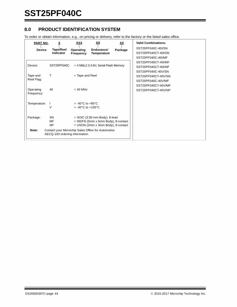
8.0 PRODUCT IDENTIFICATION SYSTEM
To order or obtain information, e.g., on pricing or delivery, refer to the factory or the listed sales office.
PART NO. XXX XX
Endurance/Operating Device
Device: SST25PF040C = 4 Mbit,2.3-3.6V, Serial Flash Memory
Tape and Reel Flag:
T = Tape and Reel
Operating Frequency:
40 = 40 MHz
Temperature: I = -40°C to +85°CV = -40°C to +105°C
Package: SN = SOIC (3.90 mm Body), 8-leadMF = WDFN (5mm x 6mm Body), 8-contactNP = USON (2mm x 3mm Body), 8-contact
Note: Contact your Microchip Sales Office for Automotive AECQ-100 ordering information.
Valid Combinations:
SST25PF040C-40I/SN
SST25PF040CT-40I/SN
SST25PF040C-40I/MF
SST25PF040CT-40I/MF
SST25PF040CT-40I/NP
SST25PF040C-40V/SN
SST25PF040CT-40V/SN
SST25PF040C-40V/MF
SST25PF040CT-40V/MF
SST25PF040CT-40V/NP
X
Tape/ReelIndicator Frequency
XX
PackageTemperature
Note the following details of the code protection feature on Microchip devices:
• Microchip products meet the specification contained in their particular Microchip Data Sheet.
• Microchip believes that its family of products is one of the most secure families of its kind on the market today, when used in the intended manner and under normal conditions.
• There are dishonest and possibly illegal methods used to breach the code protection feature. All of these methods, to our knowledge, require using the Microchip products in a manner outside the operating specifications contained in Microchip’s Data Sheets. Most likely, the person doing so is engaged in theft of intellectual property.
• Microchip is willing to work with the customer who is concerned about the integrity of their code.
• Neither Microchip nor any other semiconductor manufacturer can guarantee the security of their code. Code protection does not mean that we are guaranteeing the product as “unbreakable.”
Code protection is constantly evolving. We at Microchip are committed to continuously improving the code protection features of ourproducts. Attempts to break Microchip’s code protection feature may be a violation of the Digital Millennium Copyright Act. If such actsallow unauthorized access to your software or other copyrighted work, you may have a right to sue for relief under that Act.
Information contained in this publication regarding deviceapplications and the like is provided only for your convenienceand may be superseded by updates. It is your responsibility toensure that your application meets with your specifications.MICROCHIP MAKES NO REPRESENTATIONS ORWARRANTIES OF ANY KIND WHETHER EXPRESS ORIMPLIED, WRITTEN OR ORAL, STATUTORY OROTHERWISE, RELATED TO THE INFORMATION,INCLUDING BUT NOT LIMITED TO ITS CONDITION,QUALITY, PERFORMANCE, MERCHANTABILITY ORFITNESS FOR PURPOSE. Microchip disclaims all liabilityarising from this information and its use. Use of Microchipdevices in life support and/or safety applications is entirely atthe buyer’s risk, and the buyer agrees to defend, indemnify andhold harmless Microchip from any and all damages, claims,suits, or expenses resulting from such use. No licenses areconveyed, implicitly or otherwise, under any Microchipintellectual property rights unless otherwise stated.
2015-2017 Microchip Technology Inc.
Microchip received ISO/TS-16949:2009 certification for its worldwide headquarters, design and wafer fabrication facilities in Chandler and Tempe, Arizona; Gresham, Oregon and design centers in California and India. The Company’s quality system processes and procedures are for its PIC® MCUs and dsPIC® DSCs, KEELOQ® code hopping devices, Serial EEPROMs, microperipherals, nonvolatile memory and analog products. In addition, Microchip’s quality system for the design and manufacture of development systems is ISO 9001:2000 certified.
QUALITY MANAGEMENT SYSTEM CERTIFIED BY DNV
== ISO/TS 16949 ==
Trademarks
The Microchip name and logo, the Microchip logo, AnyRate, AVR, AVR logo, AVR Freaks, BeaconThings, BitCloud, CryptoMemory, CryptoRF, dsPIC, FlashFlex, flexPWR, Heldo, JukeBlox, KEELOQ, KEELOQ logo, Kleer, LANCheck, LINK MD, maXStylus, maXTouch, MediaLB, megaAVR, MOST, MOST logo, MPLAB, OptoLyzer, PIC, picoPower, PICSTART, PIC32 logo, Prochip Designer, QTouch, RightTouch, SAM-BA, SpyNIC, SST, SST Logo, SuperFlash, tinyAVR, UNI/O, and XMEGA are registered trademarks of Microchip Technology Incorporated in the U.S.A. and other countries.
ClockWorks, The Embedded Control Solutions Company, EtherSynch, Hyper Speed Control, HyperLight Load, IntelliMOS, mTouch, Precision Edge, and Quiet-Wire are registered trademarks of Microchip Technology Incorporated in the U.S.A.
Adjacent Key Suppression, AKS, Analog-for-the-Digital Age, Any Capacitor, AnyIn, AnyOut, BodyCom, chipKIT, chipKIT logo, CodeGuard, CryptoAuthentication, CryptoCompanion, CryptoController, dsPICDEM, dsPICDEM.net, Dynamic Average Matching, DAM, ECAN, EtherGREEN, In-Circuit Serial Programming, ICSP, Inter-Chip Connectivity, JitterBlocker, KleerNet, KleerNet logo, Mindi, MiWi, motorBench, MPASM, MPF, MPLAB Certified logo, MPLIB, MPLINK, MultiTRAK, NetDetach, Omniscient Code Generation, PICDEM, PICDEM.net, PICkit, PICtail, PureSilicon, QMatrix, RightTouch logo, REAL ICE, Ripple Blocker, SAM-ICE, Serial Quad I/O, SMART-I.S., SQI, SuperSwitcher, SuperSwitcher II, Total Endurance, TSHARC, USBCheck, VariSense, ViewSpan, WiperLock, Wireless DNA, and ZENA are trademarks of Microchip Technology Incorporated in the U.S.A. and other countries.
SQTP is a service mark of Microchip Technology Incorporated in the U.S.A.
Silicon Storage Technology is a registered trademark of Microchip Technology Inc. in other countries.
GestIC is a registered trademark of Microchip Technology Germany II GmbH & Co. KG, a subsidiary of Microchip Technology Inc., in other countries.
All other trademarks mentioned herein are property of their respective companies.
© 2015-2017, Microchip Technology Incorporated, All Rights Reserved.
ISBN: 978-1-5224-1488-9
DS20005397C-page 45
DS20005397C-page 46 2015-2017 Microchip Technology Inc.
AMERICASCorporate Office2355 West Chandler Blvd.Chandler, AZ 85224-6199Tel: 480-792-7200 Fax: 480-792-7277Technical Support: http://www.microchip.com/supportWeb Address: www.microchip.com
AtlantaDuluth, GA Tel: 678-957-9614 Fax: 678-957-1455
Austin, TXTel: 512-257-3370
BostonWestborough, MA Tel: 774-760-0087 Fax: 774-760-0088
ChicagoItasca, IL Tel: 630-285-0071 Fax: 630-285-0075
DallasAddison, TX Tel: 972-818-7423 Fax: 972-818-2924
DetroitNovi, MI Tel: 248-848-4000
Houston, TX Tel: 281-894-5983
IndianapolisNoblesville, IN Tel: 317-773-8323Fax: 317-773-5453Tel: 317-536-2380
Los AngelesMission Viejo, CA Tel: 949-462-9523Fax: 949-462-9608Tel: 951-273-7800
Raleigh, NC Tel: 919-844-7510
New York, NY Tel: 631-435-6000
San Jose, CA Tel: 408-735-9110Tel: 408-436-4270
Canada - TorontoTel: 905-695-1980 Fax: 905-695-2078
ASIA/PACIFICAsia Pacific OfficeSuites 3707-14, 37th FloorTower 6, The GatewayHarbour City, Kowloon
Hong KongTel: 852-2943-5100Fax: 852-2401-3431
Australia - SydneyTel: 61-2-9868-6733Fax: 61-2-9868-6755
China - BeijingTel: 86-10-8569-7000 Fax: 86-10-8528-2104
China - ChengduTel: 86-28-8665-5511Fax: 86-28-8665-7889
China - ChongqingTel: 86-23-8980-9588Fax: 86-23-8980-9500
China - DongguanTel: 86-769-8702-9880
China - GuangzhouTel: 86-20-8755-8029
China - HangzhouTel: 86-571-8792-8115 Fax: 86-571-8792-8116
China - Hong Kong SARTel: 852-2943-5100 Fax: 852-2401-3431
China - NanjingTel: 86-25-8473-2460Fax: 86-25-8473-2470
China - QingdaoTel: 86-532-8502-7355Fax: 86-532-8502-7205
China - ShanghaiTel: 86-21-3326-8000 Fax: 86-21-3326-8021
China - ShenyangTel: 86-24-2334-2829Fax: 86-24-2334-2393
China - ShenzhenTel: 86-755-8864-2200 Fax: 86-755-8203-1760
China - WuhanTel: 86-27-5980-5300Fax: 86-27-5980-5118
China - XianTel: 86-29-8833-7252Fax: 86-29-8833-7256
ASIA/PACIFICChina - XiamenTel: 86-592-2388138 Fax: 86-592-2388130
China - ZhuhaiTel: 86-756-3210040 Fax: 86-756-3210049
India - BangaloreTel: 91-80-3090-4444 Fax: 91-80-3090-4123
India - New DelhiTel: 91-11-4160-8631Fax: 91-11-4160-8632
India - PuneTel: 91-20-3019-1500
Japan - OsakaTel: 81-6-6152-7160 Fax: 81-6-6152-9310
Japan - TokyoTel: 81-3-6880- 3770 Fax: 81-3-6880-3771
Korea - DaeguTel: 82-53-744-4301Fax: 82-53-744-4302
Korea - SeoulTel: 82-2-554-7200Fax: 82-2-558-5932 or 82-2-558-5934
Malaysia - Kuala LumpurTel: 60-3-6201-9857Fax: 60-3-6201-9859
Malaysia - PenangTel: 60-4-227-8870Fax: 60-4-227-4068
Philippines - ManilaTel: 63-2-634-9065Fax: 63-2-634-9069
SingaporeTel: 65-6334-8870Fax: 65-6334-8850
Taiwan - Hsin ChuTel: 886-3-5778-366Fax: 886-3-5770-955
Taiwan - KaohsiungTel: 886-7-213-7830
Taiwan - TaipeiTel: 886-2-2508-8600 Fax: 886-2-2508-0102
Thailand - BangkokTel: 66-2-694-1351Fax: 66-2-694-1350
EUROPEAustria - WelsTel: 43-7242-2244-39Fax: 43-7242-2244-393
Denmark - CopenhagenTel: 45-4450-2828 Fax: 45-4485-2829
Finland - EspooTel: 358-9-4520-820
France - ParisTel: 33-1-69-53-63-20 Fax: 33-1-69-30-90-79
France - Saint CloudTel: 33-1-30-60-70-00
Germany - GarchingTel: 49-8931-9700Germany - HaanTel: 49-2129-3766400
Germany - HeilbronnTel: 49-7131-67-3636
Germany - KarlsruheTel: 49-721-625370
Germany - MunichTel: 49-89-627-144-0 Fax: 49-89-627-144-44
Germany - RosenheimTel: 49-8031-354-560
Israel - Ra’anana Tel: 972-9-744-7705
Italy - Milan Tel: 39-0331-742611 Fax: 39-0331-466781
Italy - PadovaTel: 39-049-7625286
Netherlands - DrunenTel: 31-416-690399 Fax: 31-416-690340
Norway - TrondheimTel: 47-7289-7561
Poland - WarsawTel: 48-22-3325737
Romania - BucharestTel: 40-21-407-87-50
Spain - MadridTel: 34-91-708-08-90Fax: 34-91-708-08-91
Sweden - GothenbergTel: 46-31-704-60-40
Sweden - StockholmTel: 46-8-5090-4654
UK - WokinghamTel: 44-118-921-5800Fax: 44-118-921-5820
Worldwide Sales and Service
11/07/16


