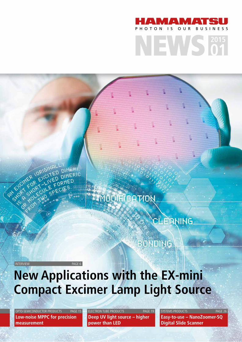
New Applications with the EX-mini Compact Excimer Lamp Light Source
IntervIew PAGe 6
Low-noise MPPC for precision measurement
OPtO-SeMICOnDUCtOr PrODUCtS PAGe 15
Deep UV light source – higher power than LED
eLeCtrOn tUBe PrODUCtS PAGe 19
Easy-to-use – NanoZoomer-SQ Digital Slide Scanner
SYSteMS PrODUCtS PAGe 26
2015
01

June 22-25, 2015Munich, GermanyHall A2, Booth 303
PHOTONNOVATION
3news 2015 vol. 1
Academ
ic rese
arch
nD Inspe
ction
Indust
ry
Secu
rity
Optical
Comms
Semico
nd. P
rod.
Analyt
ical
Measur
emen
t
Drug Disc
overy
Life S
cienc
e
Medica
l
COMPAnY newS
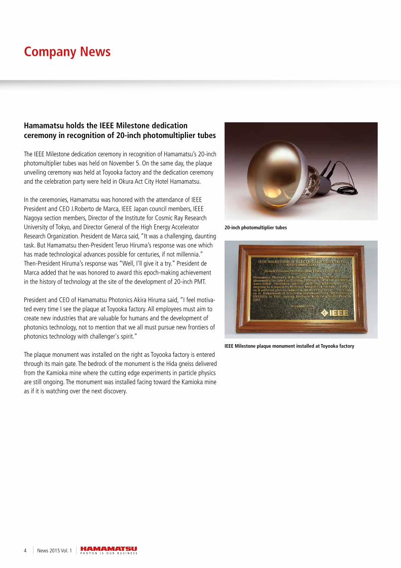
4 Hamamatsu holds the Ieee Milestone dedication ceremony
in recognition of 20-inch photomultiplier tubes
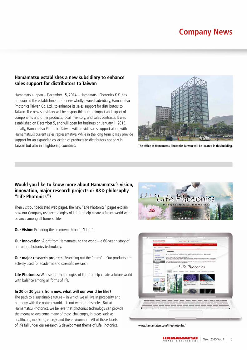
5 Hamamatsu establishes a new subsidiary to enhance sales
support for distributors to taiwan
5 would you like to know more about Hamamatsu’s vision,
innovation, major research projects or r&D philosophy
“Life Photonics”?
COver StOrY – IntervIew
6 the eX-mini compact excimer lamp light source
All the great features of excimer lamps in one compact package!
APPLICAtIOn rePOrt
10 tumor detection in fluorescent tissue microarrays enables high-through-
put analysis of multiple cancer biomarkers
12 Investigations of emission quantum yields of blue, green, and red emitting
organo-metallic complexes in a wide temperature range
USB3.0 eXtenDerS fOr USe wItH HAMAMAtSU USB3.0 CAMerAS
14 Advanced USB solution
ServICeS
30 Global exhibitions 2015
31 Hamamatsu Photonics K.K. Sales Offices
Content
OPTO-SEMICONDUCTOR PRODUCTS
15 MPPC®/MPPC Module S13360 Series, C13365/C13366 Series
16 CMOS Linear Image Sensor S13131
17 Mini-spectrometer C13053MA
18 InAsSb Photovoltaic Detector (non-cooled type) P13243 Series
ELECTRON TUBE PRODUCTS
19 Deep Uv Light Source (UvCL) L12848-305
20 excimer Lamp Light Source L11751-01, e12499, C11997
21 Opto-Spectrum Generator L12194-00-34054
22 nIr-PMt Unit H12397-75
23 fast Decay time Phosphor J12782-09D
SYSTEMS PRODUCTS
24 OrCA-flash4.0 Lt with w-vIew Mode™
26 nanoZoomer-SQ Digital Slide Scanner C13140-21
27 ImageM X2-1K eM-CCD Camera C9100-24B
LASER PRODUCTS
28 LD Irradiation Light Source (SPOLD) L11785-61
29 Super Luminescent Diode (SLD) L12856-04
News 2015 Vol. 14
Company News
Hamamatsu holds the IEEE Milestone dedication ceremony in recognition of 20-inch photomultiplier tubes
the Ieee Milestone dedication ceremony in recognition of Hamamatsu’s 20-inch photomultiplier tubes was held on november 5. On the same day, the plaque unveiling ceremony was held at toyooka factory and the dedication ceremony and the celebration party were held in Okura Act City Hotel Hamamatsu. In the ceremonies, Hamamatsu was honored with the attendance of Ieee President and CeO J.roberto de Marca, Ieee Japan council members, Ieee nagoya section members, Director of the Institute for Cosmic ray research University of tokyo, and Director General of the High energy Accelerator research Organization. President de Marca said, “It was a challenging, daun ting task. But Hamamatsu then-President teruo Hiruma’s response was one which has made technological advances possible for centuries, if not millennia.” then-President Hiruma’s response was “well, I’ll give it a try.” President de Marca added that he was honored to award this epoch-making achievement in the history of technology at the site of the development of 20-inch PMt. President and CeO of Hamamatsu Photonics Akira Hiruma said, “I feel motiva-ted every time I see the plaque at toyooka factory. All employees must aim to create new industries that are valuable for humans and the development of photonics technology, not to mention that we all must pursue new frontiers of photonics technology with challenger's spirit.” the plaque monument was installed on the right as toyooka factory is entered through its main gate. the bedrock of the monument is the Hida gneiss delivered from the Kamioka mine where the cutting edge experiments in particle physics are still ongoing. the monument was installed facing toward the Kamioka mine as if it is watching over the next discovery.
20-inch photomultiplier tubes
IEEE Milestone plaque monument installed at Toyooka factory
5News 2015 Vol. 1
Company News
Hamamatsu establishes a new subsidiary to enhance sales support for distributors to Taiwan
Hamamatsu, Japan – December 15, 2014 – Hamamatsu Photonics K.K. has announced the establishment of a new wholly-owned subsidiary, Hamamatsu Photonics taiwan Co. Ltd., to enhance its sales support for distributors to taiwan. the new subsidiary will be responsible for the import and export of components and other products, local inventory, and sales contracts. It was established on December 5, and will open for business on January 1, 2015. Initially, Hamamatsu Photonics taiwan will provide sales support along with Hamamatsu’s current sales representative, while in the long term it may provide support for an expanded collection of products to distributors not only in taiwan but also in neighboring countries. The office of Hamamatsu Photonics Taiwan will be located in this building.
www.hamamatsu.com/lifephotonics/
Would you like to know more about Hamamatsu’s vision, innovation, major research projects or R&D philosophy “Life Photonics”?
then visit our dedicated web pages. the new “Life Photonics” pages explain how our Company use technologies of light to help create a future world with balance among all forms of life.
Our Vision: exploring the unknown through “Light”.
Our Innovation: A gift from Hamamatsu to the world – a 60-year history of nurturing photonics technology.
Our major research projects: Searching out the “truth” – Our products are actively used for academic and scientific research.
Life Photonics: we use the technologies of light to help create a future world with balance among all forms of life.
In 20 or 30 years from now, what will our world be like? the path to a sustainable future – in which we all live in prosperity and harmony with the natural world – is not without obstacles. But at Hamamatsu Photonics, we believe that photonics technology can provide the means to overcome many of these challenges, in areas such as healthcare, medicine, energy, and the environment. All of these facets of life fall under our research & development theme of Life Photonics.
News 2015 Vol. 16
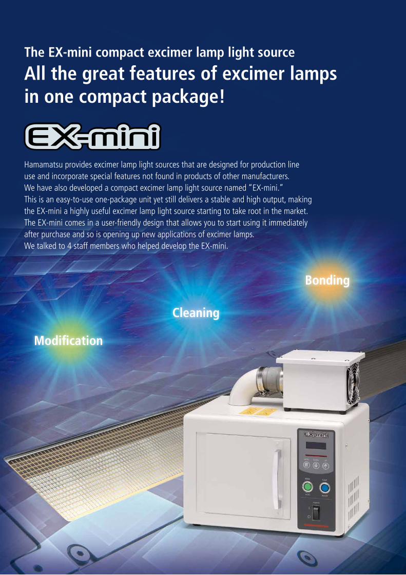
All the great features of excimer lamps in one compact package!
Hamamatsu provides excimer lamp light sources that are designed for production lineuse and incorporate special features not found in products of other manufacturers. we have also developed a compact excimer lamp light source named “eX-mini.” this is an easy-to-use one-package unit yet still delivers a stable and high output, making the eX-mini a highly useful excimer lamp light source starting to take root in the market. the eX-mini comes in a user-friendly design that allows you to start using it immediately after purchase and so is opening up new applications of excimer lamps. we talked to 4 staff members who helped develop the eX-mini.
Modification
Cleaning
Bonding
The EX-mini compact excimer lamp light source
7News 2015 Vol. 1
Interview
HAMAMATSU excimer lamp light sources
Solving the problems of competing products and getting a foothold in the market
Hello everyone, could you start off by telling us about the special features and unique points of excimer lamps?Onoda: the excimer lamp is a light source that allows modification and cleaning materials by vacuum ultraviolet light. Corona discharge /plasma treatment can do the same tasks, but they discharge directly onto the material and so it might possibly get damaged by them.
Miyamoto: the excimer lamp emits only vacuum ultraviolet light and so causes virtually no damage to the material. It is also a clean process generating no dust particles. One great feature is that it applies a uniform processing effect over a large surface area.
What makes the Hamamatsu excimer lamps unique compared to other company products?Onoda: Our company started the development and production of excimer lamps after other manufacturers. to enter the excimer lamp market, we took advantage of long years of accomplishment amassed from developing other light sources such as xenon lamps, and solved the problems of the products that had already been used.
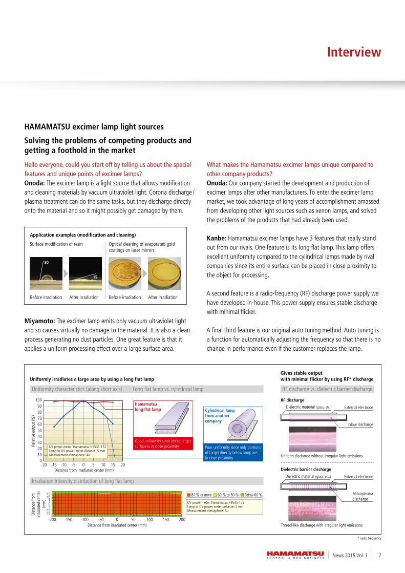
Kanbe: Hamamatsu excimer lamps have 3 features that really stand out from our rivals. One feature is its long flat lamp. this lamp offers excellent uniformity compared to the cylindrical lamps made by rival companies since its entire surface can be placed in close proximity to the object for processing.
A second feature is a radio-frequency (rf) discharge power supply we have developed in-house. this power supply ensures stable discharge with minimal flicker.
A final third feature is our original auto tuning method. Auto tuning is a function for automatically adjusting the frequency so that there is no change in performance even if the customer replaces the lamp.
Application examples (modification and cleaning)
Uniformly irradiates a large area by using a long flat lampGives stable output with minimal flicker by using RF* discharge
Surface modification of resin Optical cleaning of evaporated gold coatings on laser mirrors
Before irradiation Before irradiationAfter irradiation After irradiation
80
15
-20 -150
102030405060708090
100
-10 -5 0 5Distance from irradiated center (mm)
Rela
tive
outp
ut (%
)
10 15 20
UV power meter: Hamamatsu H9535-172Lamp to UV power meter distance: 5 mmMeasurement atmosphere: Air
Good uniformity since entire target surface is in close proximity
Hamamatsu long flat lamp
Poor uniformity since only portions of target directly below lamp are in close proximity
Cylindrical lamp from another company
UV power meter: Hamamatsu H9535-172Lamp to UV power meter distance: 5 mmMeasurement atmosphere: Air
* radio frequency
Dielectric barrier discharge
RF discharge
Dielectric material (glass, etc.) External electrode
Dielectric material (glass, etc.) External electrode
Thread-like discharge with irregular light emissions
Uniform discharge without irregular light emissions
-15-10-505
1015
0Distance from irradiated center (mm)
Dist
ance
from
irr
adia
ted
cent
er
(mm
)
50-50 100-100 150-150 200-200
80 % or more 60 % to 80 % Below 60 %
Microplasma discharge
Glow discharge
Uniformity characteristics (along short axis) Long flat lamp vs. cylindrical lamp
Irradiation intensity distribution of long flat lamp
-20 -150
102030405060708090
100
-10 -5 0 5Distance from irradiated center (mm)
Rela
tive
outp
ut (%
)
10 15 20
UV power meter: Hamamatsu H9535-172Lamp to UV power meter distance: 5 mmMeasurement atmosphere: Air
Good uniformity since entire target surface is in close proximity
Hamamatsu long flat lamp
Poor uniformity since only portions of target directly below lamp are in close proximity
Cylindrical lamp from another company
UV power meter: Hamamatsu H9535-172Lamp to UV power meter distance: 5 mmMeasurement atmosphere: Air
* radio frequency
Dielectric barrier discharge
RF discharge
Dielectric material (glass, etc.) External electrode
Dielectric material (glass, etc.) External electrode
Thread-like discharge with irregular light emissions
Uniform discharge without irregular light emissions
-15-10-505
1015
0Distance from irradiated center (mm)
Dist
ance
from
irr
adia
ted
cent
er
(mm
)
50-50 100-100 150-150 200-200
80 % or more 60 % to 80 % Below 60 %
Microplasma discharge
Glow discharge
-20 -150
102030405060708090
100
-10 -5 0 5Distance from irradiated center (mm)
Rela
tive
outp
ut (%
)
10 15 20
UV power meter: Hamamatsu H9535-172Lamp to UV power meter distance: 5 mmMeasurement atmosphere: Air
Good uniformity since entire target surface is in close proximity
Hamamatsu long flat lamp
Poor uniformity since only portions of target directly below lamp are in close proximity
Cylindrical lamp from another company
UV power meter: Hamamatsu H9535-172Lamp to UV power meter distance: 5 mmMeasurement atmosphere: Air
* radio frequency
Dielectric barrier discharge
RF discharge
Dielectric material (glass, etc.) External electrode
Dielectric material (glass, etc.) External electrode
Thread-like discharge with irregular light emissions
Uniform discharge without irregular light emissions
-15-10
-505
1015
0Distance from irradiated center (mm)
Dist
ance
from
irr
adia
ted
cent
er
(mm
)
50-50 100-100 150-150 200-200
80 % or more 60 % to 80 % Below 60 %
Microplasma discharge
Glow discharge
rf discharge vs. dielectric barrier discharge
* radio frequency
-20 -150
102030405060708090
100
-10 -5 0 5Distance from irradiated center (mm)
Rela
tive
outp
ut (%
)
10 15 20
UV power meter: Hamamatsu H9535-172Lamp to UV power meter distance: 5 mmMeasurement atmosphere: Air
Good uniformity since entire target surface is in close proximity
Hamamatsu long flat lamp
Poor uniformity since only portions of target directly below lamp are in close proximity
Cylindrical lamp from another company
UV power meter: Hamamatsu H9535-172Lamp to UV power meter distance: 5 mmMeasurement atmosphere: Air
* radio frequency
Dielectric barrier discharge
RF discharge
Dielectric material (glass, etc.) External electrode
Dielectric material (glass, etc.) External electrode
Thread-like discharge with irregular light emissions
Uniform discharge without irregular light emissions
-15-10
-505
1015
0Distance from irradiated center (mm)
Dist
ance
from
irr
adia
ted
cent
er
(mm
)
50-50 100-100 150-150 200-200
80 % or more 60 % to 80 % Below 60 %
Microplasma discharge
Glow discharge

News 2015 Vol. 18
Currently how many product types do you have on the market?Sakuma: we initially released products mainly for use on production lines. But in July 2013, we put the compact one-package eX-mini which was developed for the laboratory and other tasks on the market. Our sales are now steadily expanding.
Onoda: Customers presented us with a long list of needs in various fields such as adhesive and coating preprocessing and improving the wettability prior to the ink coating process. Many different cases are being evaluated to determine if we can actually meet customer needs or not.
Miyamoto: the prototype for the eX-mini was a demo model of excimer lamp light source developed for production line use. we de signed the demo model to show at events such as exhibits where customers could experience the performance of our excimer lamps. After checking out our one-package light source, customers found out how handy and versatile it really was, and said “this is the one we want.”
Sakuma: Questioning the customer in more detail revealed that up till now they had been separately purchasing power supplies, light sources and irradiation boxes, and making their own devices by hand for use in laboratories and elsewhere. But, if these could all be offered in one package, then they could buy it and start using it right away. this convenience was what they rated so highly.
Onoda: On learning this, we redesigned that original demo model in terms of safety and user operability to develop what is now the eX-mini. we also added an ozone decomposition unit at that time as an option.
Sakuma: Using an excimer lamp generates ozone, so joining the
equipment to an exhaust duct is necessary. But, this restricts the locations where the equipment can be mounted and also requires installing a duct. to eliminate this inconvenience, we designed an ozone decomposition unit capable of breaking down the ozone according to the amount generated.
Miyamoto: Comparing the eX-mini to compact excimer lamps made by rival companies reveals that the eX-mini has at least a 5 times greater output. Besides the convenience of being usable right after purchase, the huge boost in operating efficiency also offers a big advantage to the customer.
we never even considered giving up on our “same power in small body” concept
Where did you run into a lot of trouble when developing the EX-mini?Sakuma: the eX-mini was rated as a device for assessing production line usage and we clung to the concept that its output must be equivalent to that of the current model used on production lines.
Kanbe: Making the device small also required changing the internal wiring. Utilizing a big lamp requires virtually no changes in the wiring
CO2
O2
O3
O3
O3
O3
H2O
Ozone
Clean air
Ozone decomposition unit
Interview
Ozone decomposition unit
For production line For R&D
9News 2015 Vol. 1
Interview
but using a small lamp would affect the output due to the wiring. So we kept struggling down to the final stages with the thorny problem of using a small size lamp but with no drop in output.
Onoda: we hadn’t solved this output problem yet even after more than half the development period had elapsed. At product exhibits, customers who saw the demo models insisted they needed a small device as soon as possible, so this kept us tense and on edge when looking for a solution.
Sakuma: In the end, things weren’t quite so dramatic. we kept modifying the power supply and improving the lamp and finally achieved both a small unit and a satisfactory output.
expansion of the Point of Care testing (POCt) market has broadened applications to include microfluidic devices
What future applications do you foresee for the EX-mini?Onoda: excimer lamps have usually been used by materials manufacturers for developing new types of materials and cleaning of specialized materials. As one new type of application from hereon, we foresee a demand for microfluidic devices.
Sakuma: More specifically, we believe that excimer lamps can contribute to processes for manufacturing microfluidic devices that are gradually becoming feasible in medical and bio-science fields. Microfluidic devices align and bond diverse types of materials together and form tiny flow paths along which chemical reagents flow. If we used the eX-mini to do this, then microfluidic devices could likely be
made easily with a high degree of bonding accuracy compared to conventional manufacturing processing that uses adhesive agents.
Miyamoto: Looking towards the future, we expect the POCt (Point of Care testing) market to expand and are moving ahead with product evaluations for this field. Other areas where we anticipate new usage of microfluidic devices include protein and DnA analysis, drug discovery support, cell experiments, and chemical monitoring.
How will excimer lamps from Hamamatsu evolve from now on and in what direction?Sakuma: the first step to take is getting a lot of requests and needs from customers and moving to respond to those requests. there is a whole stack of issues remaining to be tackled including a long lamp service life, developing further lamp variations, and boosting lamp processing capability and throughput capacity.
Onoda: Our excimer lamps get a great deal of attention from customers when put on display at exhibits and shows, and this makes us feel that excimer lamps have a lot of advantages to offer. After perfecting this compact laboratory model, we will shift our focus towards designing compact models for use on production lines.
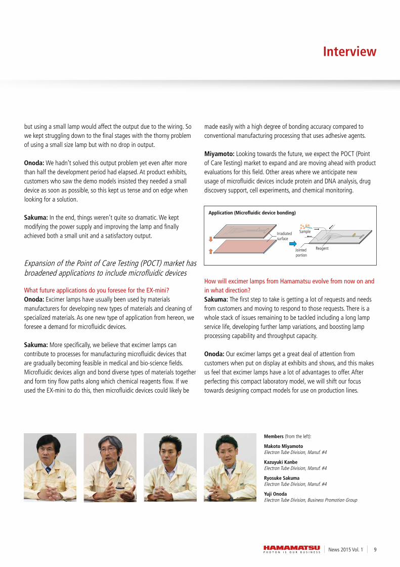
Members (from the left):
Makoto Miyamoto electron tube Division, Manuf. #4
Kazuyuki Kanbe electron tube Division, Manuf. #4
Ryosuke Sakuma electron tube Division, Manuf. #4
Yuji Onoda electron tube Division, Business Promotion Group
Irradiated surface
Jointed portion
Reagent
Sample
Application (Microfluidic device bonding)

News 2015 Vol. 110
Application Report
Tumor detection in fluorescent tissue microarrays enables high-throughput analysis of multiple cancer biomarkers
Automation in immunohistological image processing is currently an essential technological development taking place in the clinical hunt for objective biomarkers in research and diagnostics. In cancer research one of the most important but also extreme challenges is the develop ment of methods for the automatic separation of tumor and stroma tissue.
An important method routinely used in this context is the tissue Microarray (tMA) technology, introduced in 1998. tMAs allow the simulta neous immunohistochemical analysis of several hundred tissues on a single slide. the manual detection of tumor regions in tissue Micro arrays is routinely based on the quantitative analysis of protein levels by pathologists or other experts. Yet manual detection is subjective, time consuming and most importantly suffers from intra and inter-observer variability.
A route to objectivity in histological tumor evaluation is automation and quantification by software routines. this will require computa-tional methods capable of automatically identifying tumor areas and differen tia ting them from the stroma in a high quality microscopic image of the tissue, obtained by a virtual slide scanner.
"to overcome the key problems of bright field staining caused by the objective and automatic capturing of distinct biomarker signals, we use fluorescence staining", PD Dr.-Ing. niels Grabe, Scientific Head of the tIGA center explains. Although fluorescence helps in the quanti-fi cation of individual cells, it does not as such help in differentiating tumor and stroma. Consequently fluorescence stained tissue slides are frequently counterstained with DAPI (4’6-diamidino-2-phenylindole) taking the role of a conventional background stain.
"for scanning our fluorescence stained tMAs we used the nanoZoomer 2.0 Ht scan system capable of scanning whole slides in high resolu-tion", Bernd Lahrmann (PhD student) explains. Glass slides were scanned at 20x magnification (resolution of 0.46µm/pixel). the slide scanner auto matically detects the region of interest that contains the array of cores and also determines automatically a valid focal plane for scanning. Single core images were located and extracted from the tMAs using template matching.
"As no histological biomarker is available which would exclusively stain tumor tissue, pathology routinely uses morphological criteria as a spatial reference system. to combine the advantages of fluorescence with automatic image acquisition and processing we developed an algorithm for tumor-stroma separation and classification in immuno-fluorescence histological slides solely from a DAPI background stain", explains Bernd Lahrmann.
Due to the restriction to a single color channel this is inherently challen ging. we formed cell graphs based on the topological distri bu-tion of the tissue cell nuclei and extracted the corresponding graph features. By using topological, morphological and intensity based features we could systematically quantify and compare the discrimina-tion capability individual features contribute to the overall algorithm. we found that when classifying fluorescence tissue slides in the DAPI channel, morphological and intensity based features clearly outpace topological ones which have been used exclusively in related previous
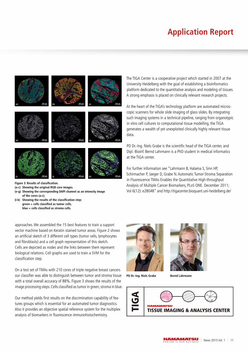
Figure 1: Microscopic image examples of TMA slides (left) and cores (right).Representation of all 3 channels of a fluorescence stained core in RGB colour space. Red representing stromal marker (CK19), green the tumor marker (Vimentin) and blue the DAPI channel highlighting the cell nuclei.
Figure 2: Conceptional representation of cell graphs. (a) Artificial sketch of three different cell types:
tumor cells (blue), lymphocytes (white) and fibroblast (purple). (b) Cell graph representation of (a). Cells are depicted as nodes
and the links between them represent biological relations.
(a) (b)
11News 2015 Vol. 1
Application Report
approaches. we assembled the 15 best features to train a support vector machine based on Keratin stained tumor areas. figure 2 shows an artificial sketch of 3 different cell types (tumor cells, lymphocytes and fibroblasts) and a cell graph representation of this sketch. Cells are depicted as nodes and the links between them represent biological relations. Cell graphs are used to train a SvM for the classification step.
On a test set of tMAs with 210 cores of triple negative breast cancers our classifier was able to distinguish between tumor and stroma tissue with a total overall accuracy of 88%. figure 3 shows the results of the image processing steps. Cells classified as tumor in green, stroma in blue.
Our method yields first results on the discrimination capability of fea-tu res groups which is essential for an automated tumor diagnostics. Also it provides an objective spatial reference system for the multiplex analysis of biomarkers in fluorescence immunohistochemistry.
(a) 200 µm (b) 200 µm (c) 200 µm
(e) 200 µm (f) 200 µm (g) 200 µm
Figure 3: Results of classification. (a-c) Showing the original RGB core images.(e-g) Showing the corresponding DAPI channel as an intensity image
of the cores (a-c).(i-k) Showing the results of the classification step: green = cells classified as tumor cells, blue = cells classified as stroma cells.
(i) 200 µm (j) 200 µm (k) 200 µm
PD Dr.-Ing. Niels Grabe Bernd Lahrmann
the tIGA Center is a cooperative project which started in 2007 at the University Heidelberg with the goal of establishing a bioinformatics platform dedicated to the quantitative analysis and modeling of tissues. A strong emphasis is placed on clinically relevant research projects.
At the heart of the tIGA’s technology platform are automated micros-copic scanners for whole slide imaging of glass slides. By integrating such imaging systems in a technical pipeline, ranging from organotypic in vitro cell cultures to computational tissue modelling, the tIGA gene rates a wealth of yet unexploited clinically highly relevant tissue data.
PD Dr.-Ing. niels Grabe is the scientific head of the tIGA center, and Dipl.-Bioinf. Bernd Lahrmann is a PhD student in medical informatics at the tIGA center.
for further information see “Lahrmann B, Halama S, Sinn HP, Schirmacher P, Jaeger D, Grabe n. Automatic tumor-Stroma Separation in fluorescence tMAs enables the Quantitative High-throughput Analysis of Multiple Cancer Biomarkers, PLoS One. December 2011; vol 6(12): e28048” and http://tigacenter.bioquant.uni-heidelberg.de/
Application Report
news 2015 vol. 112
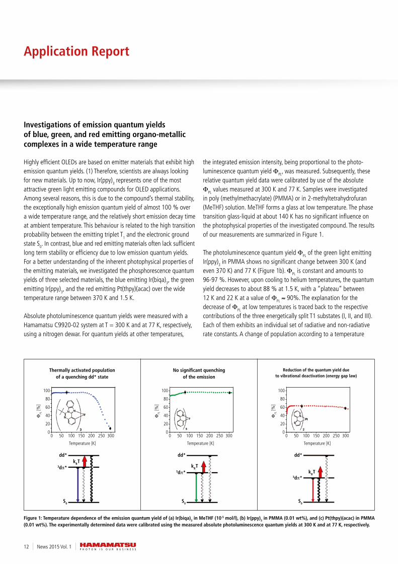
Investigations of emission quantum yields of blue, green, and red emitting organo-metallic complexes in a wide temperature range
Highly efficient OLeDs are based on emitter materials that exhibit high emission quantum yields. (1) therefore, scientists are always looking for new materials. Up to now, Ir(ppy)3 represents one of the most attractive green light emitting compounds for OLeD applications. Among several reasons, this is due to the compound’s thermal stability, the exceptionally high emission quantum yield of almost 100 % over a wide temperature range, and the relatively short emission decay time at ambient temperature. this behaviour is related to the high transition proba bility between the emitting triplet t1 and the electronic ground state S0. In contrast, blue and red emitting materials often lack suffi cient long term stability or efficiency due to low emission quan tum yields. for a better understanding of the inherent photophysical pro perties of the emitting materials, we investigated the phosphorescence quantum yields of three selected materials, the blue emitting Ir(biqa)3, the green emitting Ir(ppy)3, and the red emitting Pt(thpy)(acac) over the wide temperature range between 370 K and 1.5 K.
Absolute photoluminescence quantum yields were measured with a Hamamatsu C9920-02 system at t = 300 K and at 77 K, respectively, using a nitrogen dewar. for quantum yields at other temperatures,
the integrated emission intensity, being proportional to the photo-luminescence quantum yield ΦPL, was measured. Subsequently, these relative quantum yield data were calibrated by use of the absolute ΦPL values measured at 300 K and 77 K. Samples were investigated in poly (methylmethacrylate) (PMMA) or in 2-methyltetrahydrofuran (MetHf) solution. MetHf forms a glass at low temperature. the phase transition glass-liquid at about 140 K has no significant influence on the photophysical properties of the investigated compound. the results of our measurements are summarized in figure 1.
the photoluminescence quantum yield ΦPL of the green light emit ting Ir(ppy)3 in PMMA shows no significant change between 300 K (and even 370 K) and 77 K (figure 1b). ΦPL is constant and amounts to 96-97 %. However, upon cooling to helium temperatures, the quantum yield decreases to about 88 % at 1.5 K, with a “plateau” between 12 K and 22 K at a value of ΦPL ≈ 90%. the explanation for the decrease of ΦPL at low temperatures is traced back to the respective con tributions of the three energetically split t1 substates (I, II, and III). each of them exhibits an individual set of radiative and non-radiative rate constants. A change of population according to a temperature
Figure 1: Temperature dependence of the emission quantum yield of (a) Ir(biqa)3 in MeTHF (10-5 mol/l), (b) Ir(ppy)3 in PMMA (0.01 wt%), and (c) Pt(thpy)(acac) in PMMA (0.01 wt%). The experimentally determined data were calibrated using the measured absolute photoluminescence quantum yields at 300 K and at 77 K, respectively.
No significant quenching of the emission
Reduction of the quantum yield due to vibrational deactivation (energy gap law)
Thermally activated population of a quenching dd* state
ΦPL
[%]
temperature [K]
100
80
60
40
20
00 50 100 150 200 250 300
ΦPL
[%]
temperature [K]
100
80
60
40
20
00 50 100 150 200 250 300
ΦPL
[%]
temperature [K]
100
80
60
40
20
00 50 100 150 200 250 300
S0
3dπ*
dd*kB T
S0
3dπ*
dd*
kB T
S0
3dπ*
dd*
kB T
Application Report
13news 2015 vol. 1
change leads to different contributions of each state and thus, to a change of the overall-phosphorescence properties. (2) the blue emitting compound Ir(biqa)3 shows a different behaviour (figure 1a). the quantum yield drops drastically from 97 % near 200 K to 10 % at 300 K. this behaviour is explained to be a consequence of a thermal activation of quenching 1,3dd* states from the lowest triplet of 3dπ* character (t1 state). (3, 4) the low-temperature behavior (t < 170 K) is similar to the behaviour as described for Ir(ppy)3.
the quantum yield of Pt(thpy)(acac) is almost constant over the whole temperature range at a value of about 60 % (except below 20 K according to the influence of the t1 state splitting, see above). this lower value is, in comparison to the almost 100 % quantum yield of the other two materials (at low temperature), due to a substantial direct vibrational deactivation of the emitting triplet state according to the so-called energy gap law. (5) the smaller energy gap between the emitting triplet state and the electronic ground state causes a higher radiationless rate from t1 to S0. the non-radiative deactivation is competing with the radiative phosphorescence, resulting in a quantum yield of well below 100 % for the red light emitting Pt(thpy)(acac). (6)
In conclusion, quantum yield measurements at different temperatures can (in combination with lifetime measurements) be highly useful for an identification of deactivation paths of emitter materials. In particu-lar, also radiative and non-radiative rate constants of the transitions from the emitting triplet substates can be determined. (2) furthermore, our investigations show that the environment, i.e. the matrix cage around the emitter, strongly influences photophysical properties of emitter materials, for example, by disturbing the complex’s geometry and thus also the involved states. these effects have to be considered when trying to optimize the performance of an emitter material to be applied in OLeDs. (3, 7)
thomas Hofbeck and Hartmut Yersin, Institute for Physical Chemistry, University of regensburg, Germany
for more information please visit http://www.ur.de/~hartmut.yersine-Mail: [email protected], [email protected]
References(1) Yersin, H., Ed. Highly Efficient OLEDs with Phosphorescent Materials;
Wiley-VCH, Weinheim, 2008. (2) Hofbeck, T.; Yersin, H. Inorg. Chem. 2010, 49, 9290–9299. (3) Yersin, H.; Rausch, A. F.; Czerwieniec, R.; Hofbeck, T.; Fischer, T. Coord.
Chem. Rev. 2011, 255, 2622–2652. (4) Sajoto, T.; Djurovich, P. I.; Tamayo, A. B.; Oxgaard, J.; Goddard, W. A.;
Thompson, M. E. J. Am. Chem. Soc. 2009, 131, 9813–9822. (5) Englman, R.; Jortner, J. Mol. Phys. 1970, 18, 145–164. (6) Fischer, T.; Czerwieniec, R.; Hofbeck, T.; Osminina, M. M.; Yersin, H.
Chem. Phys. Lett. 2010, 486, 53–59. (7) Finkenzeller, W. J.; Hofbeck, T.; Thompson, M. E.; Yersin, H. Inorg. Chem.
2007, 46, 5076–5083.
News 2015 Vol. 114
Advanced USB solution
Many of Hamamatsu’s new cameras use a USB3.0 interface for connecting the camera to a computer. But as scientific setups become more and more complicated it becomes apparent that standard USB cables are not long enough to cover the distance between the camera and the PC. this is where USB3.0 extension kits come into play.
Several solutions of such USB3.0 extenders are available on the market today. they are mainly based on fiber optic cables and differ in the length available. the ones recommended in this article have been tested with an OrCA-flash4.0 v2 camera and can be recommended to be used with Hamamatsu USB3.0 cameras like the OrCA sCMOS cameras.
the test environment consisted of a PC with windows 7, 64bit OS, IOI USB3.0 interface board IOI U3-PCIe1XG202-10, DCAM API version September 2014, Hokawo application software version 2.9 pf0 and OrCA-flash4.0 v2 camera.
1. Unibrain USB3.0 Active Optical Cable
� fiber optic cable � Available lengths 20 m, 50 m and 100 m, customized lengths possible � Powered by secondary connection to USB3.0 hub � roHS2, reACH compliant � Detailed information: http://www.unibrain.com/products/ usb-3-0-active-optical-cables
2. Icron Spectra 3022 2-Port USB3.0 Multimode Fiber Extender
� Multimode fiber optic cable, LC connector type � Available lengths of up to 100 m � remote extender with integrated port hub and power supply on secondary connection
� roHS2 compliant � Detailed information: http://www.icron.com/products/icron-brand/ usb-extenders/fiber/usb-3-0-spectra-3022/
3. Icron Spectra 3001-15 1-Port USB3.0 15 m Active Extension Cable
� Active copper cable � Available length 15 m � Powered from host computer � roHS2 compliant � Detailed information: http://www.icron.com/products/icron-brand/usb-extenders/cat5/usb-3-0-spectra-3001-15/
4. Corning USB3.0 Optical Cables
� Based on fiber optic cable plus copper wire for power � Available lengths 10 m, 15 m, 30 m and 50 m � Powered from host computer � Detailed information: http://www.corning.com/opcomm/ OpticalCablesbyCorning/products/USB-3.Optical.aspx
Authors: tanja Acker and Holger Hermann, Hamamatsu Photonics Germany
Hamamatsu USB3.0 cameras
USB3.0 extenders for use with Hamamatsu USB3.0 cameras
OPtO-SeMICOnDUCtOr PrODUCtS
15News 2015 Vol. 1
MPPC®/MPPC Module S13360 Series, C13365/C13366 Series
Academ
ic res.
nD Inspe
ction
Indust
ry
Secu
rity
Optical
Comms
Semico
n Prod
.
Analyt
ical
Measur
emen
t
Drug Disc
overy
Life S
cienc
e
Medica
l
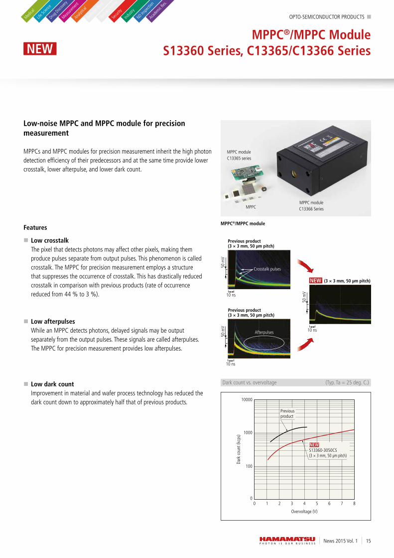
Low-noise MPPC and MPPC module for precision measurement
MPPCs and MPPC modules for precision measurement inherit the high photon detection efficiency of their predecessors and at the same time provide lower crosstalk, lower afterpulse, and lower dark count.
MPPC®/MPPC module
NEW
Dark count vs. overvoltage (typ. ta = 25 deg. C.)
Dark
cou
nt (k
cps)
Overvoltage (V)
0 1 2 3 4 875 6
10000
1000
100
0
S13360-3050CS(3 × 3 mm, 50 µm pitch)
Previousproduct
NEW
MPPC moduleC13365 series
MPPC moduleC13366 SeriesMPPC
Features
� Low crosstalk the pixel that detects photons may affect other pixels, making them produce pulses separate from output pulses. this phenomenon is called crosstalk. the MPPC for precision measurement employs a structure that suppresses the occurrence of crosstalk. this has drastically reduced crosstalk in comparison with previous products (rate of occurrence reduced from 44 % to 3 %).
� Low dark count Improvement in material and wafer process technology has reduced the dark count down to approximately half that of previous products.
� Low afterpulses while an MPPC detects photons, delayed signals may be output separately from the output pulses. these signals are called afterpulses. the MPPC for precision measurement provides low afterpulses.
Previous product (3 × 3 mm, 50 µm pitch)
10 ns
50 m
V
Crosstalk pulses
Previous product (3 × 3 mm, 50 µm pitch)
Afterpulses
50 m
V
10 ns
(3 × 3 mm, 50 µm pitch)
10 ns
50 m
V
Afterpulses
Previous product (3 × 3 mm, 50 µm pitch)
10 ns
50 m
V
Crosstalk pulses
Previous product (3 × 3 mm, 50 µm pitch)
Afterpulses
50 m
V
10 ns
(3 × 3 mm, 50 µm pitch)
10 ns
50 m
V
Afterpulses
Previous product (3 × 3 mm, 50 µm pitch)
10 ns
50 m
V
Crosstalk pulses
Previous product (3 × 3 mm, 50 µm pitch)
Afterpulses
50 m
V
10 ns
(3 × 3 mm, 50 µm pitch)
10 ns
50 m
V
Afterpulses

nD Inspe
ction
Indust
ry
Secu
rity
Optical
Comms
Semico
n Prod
.
Analyt
ical
Measur
emen
t
Drug Disc
overy
Life S
cienc
e
Medica
l
Academ
ic res.
OPtO-SeMICOnDUCtOr PrODUCtS
News 2015 Vol. 116
CMOS Linear Image Sensor S13131
Specifications
Parameter Specification Unitnumber of pixels 1,536 pixels
Pixel pitch 5.5 µm
Pixel height 63.5 µm
Photosensitive area length 8.448 mm
Spectral response range 400 to 1000 nm
Compact and thin package
the S13131 is a linear image sensor developed for barcode readers, encoders, and other various types of scanning applications. It is a COB (chip on board) type implemented in a compact (close to chip size) and thin (half the thickness of the previous product, 0.8 mm) package.
Features � Compact and thin package: 9.1 x 2.4 x 0.8 mm � High sensitivity, low noise (0.4 mv rms) � Pixel size: 5.5 x 63.5 µm � 3.3 v single power supply operation � video data rate: 2 MHz max.
Applications � Barcode reader � encoders � various types of image scanning
S13131
NEW
Package diagram (unit: mm)
Dimensional outline
Photosensitive area8.448 × 0.0635
0.3 ± 0.11
0.5 ± 0.159.1
Silicone resin Glass epoxy
0.57
± 0
.2
1 ch
Scan direction
0.3 ± 0.15
2.4
Dimensional outline
Photosensitive area8.448 × 0.0635
0.3 ± 0.11
0.5 ± 0.159.1
Silicone resin Glass epoxy
0.57
± 0
.2
1 ch
Scan direction
0.3 ± 0.15
2.4

OPtO-SeMICOnDUCtOr PrODUCtS
17News 2015 Vol. 1
Mini-spectrometer C13053MA
Academ
ic res.
nD Inspe
ction
Indust
ry
Secu
rity
Optical
Comms
Semico
n Prod
.
Analyt
ical
Measur
emen
t
Drug Disc
overy
Life S
cienc
e
Medica
l
Compact and thin, built-in high-sensitivity CMOS image sensor
the mini-spectrometer ft (flat type) series is a polychromator provided in a compact, thin case that houses optical elements, image sensor, and driver circuit. Spectrum data can be acquired by guiding measurement light into a mini-spectrometer through an optical fiber and transferring the measured results to a PC via the USB connection. the incorporation of a high-sensitivity CMOS image sensor maintains high sensitivity equivalent to that of a CCD and achieves low power consumption. Moreover, the trigger function that can be also used for short-term integration enables spectroscopic measurement of pulse emissions.
Features � Compact, thin case � High-sensitivity CMOS image sensor built in (high sensitivity equivalent to that of a CCD)
� with a trigger function � High throughput using quartz transmission grating � external power supply not necessary (USB bus powered)
Applications � Sugar content and acidity detection of foods � Plastic sorting � thickness gauge
C13053MA
Specifications
Parameter Specification UnitSpectral response range 500 to 1,100 nm
Spectral resolution (fwHM)*1typ. 2.5
nmMax. 3.5
wavelength reproducibility*2 -0.4 to +0.4 nm
wavelength temperature dependence
-0.04 to +0.04 nm/deg. C.
Spectral stray light*1, 3 -33 max. dB
A/D conversion 16 bit
Integration time 11 to 100,000 µs
Interface USB 2.0 -
USB bus power current consumption
typ. 220mA
Max. 250
*1 when the slit (25(H) x 250(v) µm) is used. the spectral resolution depends on the slit.*2 Measured under constant light input conditions.*3 the ratio of the count measured when an 800 nm light is input to the count measured when
an 800 ± 40 nm light is input.
NEW
Spectral response (ta = 25 deg. C.)
Wavelength (nm)
500 600 700 800 900 1000 1100
40
50
70
90
20
30
10
0
80
60
100
Rela
tive
sens
itivi
ty (%
)
OPtO-SeMICOnDUCtOr PrODUCtS
news 2015 vol. 118
InAsSb Photovoltaic Detector (Non-cooled Type) P13243 Series
nD Inspe
ction
Indust
ry
Secu
rity
Optical
Comms
Semico
n Prod
.
Analyt
ical
Measur
emen
t
Drug Disc
overy
Life S
cienc
e
Medica
l
Academ
ic res.
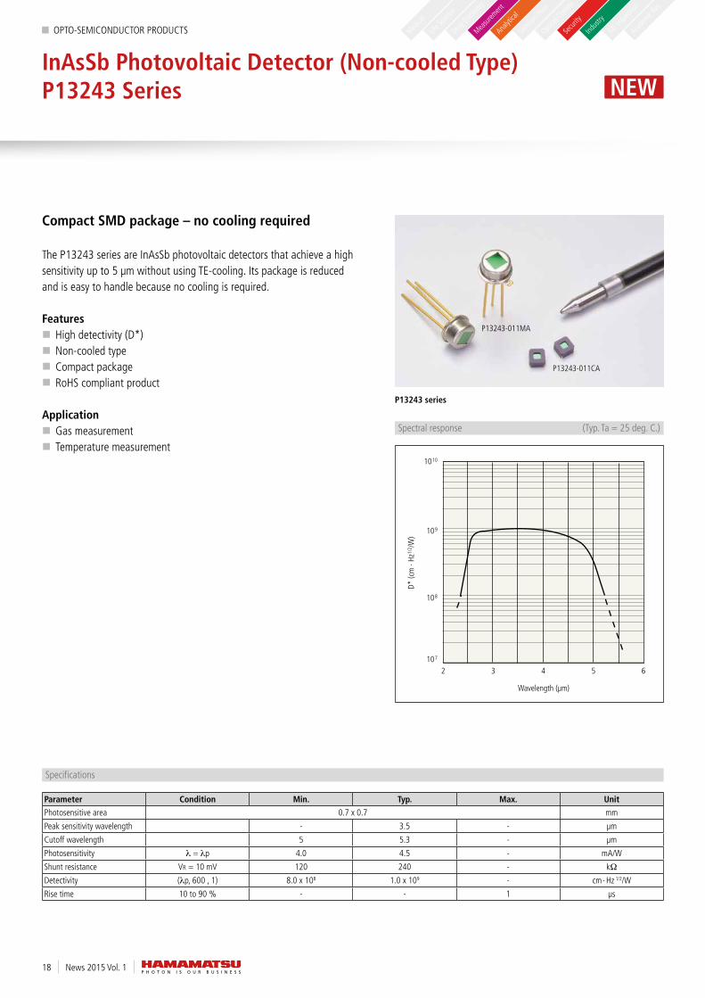
Compact SMD package – no cooling required
the P13243 series are InAsSb photovoltaic detectors that achieve a high sensitivity up to 5 µm without using te-cooling. Its package is reduced and is easy to handle because no cooling is required.
Features � High detectivity (D*) � non-cooled type � Compact package � roHS compliant product
Application � Gas measurement � temperature measurement
P13243 series
P13243-011MA
P13243-011CA
NEW
Specifications
Parameter Condition Min. Typ. Max. Unit Photosensitive area 0.7 x 0.7 mm
Peak sensitivity wavelength - 3.5 - µm
Cutoff wavelength 5 5.3 - µm
Photosensitivity λ = λp 4.0 4.5 - mA/w
Shunt resistance vr = 10 mv 120 240 - kΩ
Detectivity (λp, 600 , 1) 8.0 x 10⁸ 1.0 x 10⁹ - cm · Hz 1/2/w
rise time 10 to 90 % - - 1 µs
Spectral response (typ. ta = 25 deg. C.)
42 3 5 6107
109
108
1010
Wavelength (µm)
D* (c
m ·
Hz1/
2 /W)

eLeCtrOn tUBe PrODUCtS
19News 2015 Vol. 1
Deep UV Light Source (UVCL) L12848-305NEW
Academ
ic res.
nD Inspe
ction
Indust
ry
Secu
rity
Optical
Comms
Semico
n Prod
.
Analyt
ical
Measur
emen
t
Drug Disc
overy
Life S
cienc
e
Medica
l
Specifications
Parameter Specification UnitSpectral distribution*1 290 to 400 nm
Peak wavelength 305 nm
Light output stability*2fluctuation (p-p) (max.) 0.3 %
Drift (max.) ± 3 %/h
Guaranteed service life*2, 3 5,000 h
Light-emitting point size Approx. φ5 mm
*1 Please consult us if you need other wavelengths.*2 at 305 nm*3 Guaranteed service life is defined as the time when light intensity falls below 50 % of the initial
value or light output stability exceeds the guaranteed value.
Deep UV light source with higher power than LED
the UvCL utilizes electron beam excitation to achieve Uv output that is 8 times higher at 305 nm than a Uv-LeD and so helps improve equipment throughput. Its compact body contains a lamp, and a power supply, eliminating the need to design housing and therefore allows easy assembly into equipment.
Features � High output: 8 times higher than Uv-LeD (at 305 nm) � Compact � Mercury-free � Long service life: 5000 hours guaranteed � easy assembly into equipment � Low power consumption � no cooling required
Applications � fluorescence analysis � environmental analysis � Uv curing � Material resistance evaluation
L12848-305
Spectral distribution
250 3000
100
200
300
400
500
600
700
800
900
350 400
Wavelength (nm)
Rela
tive
irrad
ianc
e (%
)
450
LED (30 mA dc) 310 nm type
L12848-305Peak wavelength: 305 nm
Directivity (light distribution)
0
0-20-40-60-80-100 20 40 60 80 100
10 2030
-10-20-30
(deg.)
Relative intensity (%)
0
0-20-40-60-80-100 20 40 60 80 100
10 2030
-10-20-30
(deg.)
Horizontal angle
Vertical angle
Relative intensity (%)
0
0-20-40-60-80-100 20 40 60 80 100
10 2030
-10-20-30
(deg.)
Relative intensity (%)
0
0-20-40-60-80-100 20 40 60 80 100
10 2030
-10-20-30
(deg.)
Horizontal angle
Vertical angle
Relative intensity (%)
0
0-20-40-60-80-100 20 40 60 80 100
10 2030
-10-20-30
(deg.)
Relative intensity (%)
0
0-20-40-60-80-100 20 40 60 80 100
10 2030
-10-20-30
(deg.)
Horizontal angle
Vertical angle
Relative intensity (%)
0
0-20-40-60-80-100 20 40 60 80 100
10 2030
-10-20-30
(deg.)
Relative intensity (%)
0
0-20-40-60-80-100 20 40 60 80 100
10 2030
-10-20-30
(deg.)
Horizontal angle
Vertical angle
Relative intensity (%)

eLeCtrOn tUBe PrODUCtS
News 2015 Vol. 120
Excimer Lamp Light Source L11751-01, E12499, C11997
nD Inspe
ction
Indust
ry
Secu
rity
Optical
Comms
Semico
n Prod
.
Analyt
ical
Measur
emen
t
Drug Disc
overy
Life S
cienc
e
Medica
l
Academ
ic res.
Modification and cleaning by light
Unlike the excimer lamps of other manufacturers, our excimer lamp light source uses a long flat lamp that ensures uniform irradiation. Processing by light (vacuum Uv light at 172 nm) does not cause damage to objects, dust particle generation, and processing unevenness, which are usually caused by corona discharge/plasma treatment methods. the lamp has a service life that is twice as long as our current model (L11751), so it reduces maintenance costs. the power supply is designed to be more compact and lightweight and is available at a lower cost than our current model (C11753), making it a more optimal choice.
Features � Long life � Less flickering � Uniform irradiation � Instantaneous On/Off � no damage to objects � no generation of dust particles
Applications
� Surface modification • Pretreatment for adhesives (adhesive strength improvement) • Coating/printing adhesion improvement
� Material dry cleaning • Silicon wafer and glass substrate cleaning • removal of organic films/adhesive residues
� Bonding • Microfluidic device
Excimer lamp L11751-01Lamp house E12499Power supply C11997
NEW
Specifications
Parameter Specification Unitemission wavelength 172 nm
Irradiance* (min.) 50 mw/cm2
Lamp design life 2,000 h
Lamp guaranteed service life 1,000 h
Irradiation area (w x H) 400 x 38 mm
Duct suction air flow rate 0.35 ± 0.08 m3/min
* Measured with a Hamamatsu Uv power meter H9535-172
eLeCtrOn tUBe PrODUCtS
21News 2015 Vol. 1
Opto-Spectrum Generator L12194-00-34054
Academ
ic res.
nD Inspe
ction
Indust
ry
Secu
rity
Optical
Comms
Semico
n Prod
.
Analyt
ical
Measur
emen
t
Drug Disc
overy
Life S
cienc
e
Medica
l
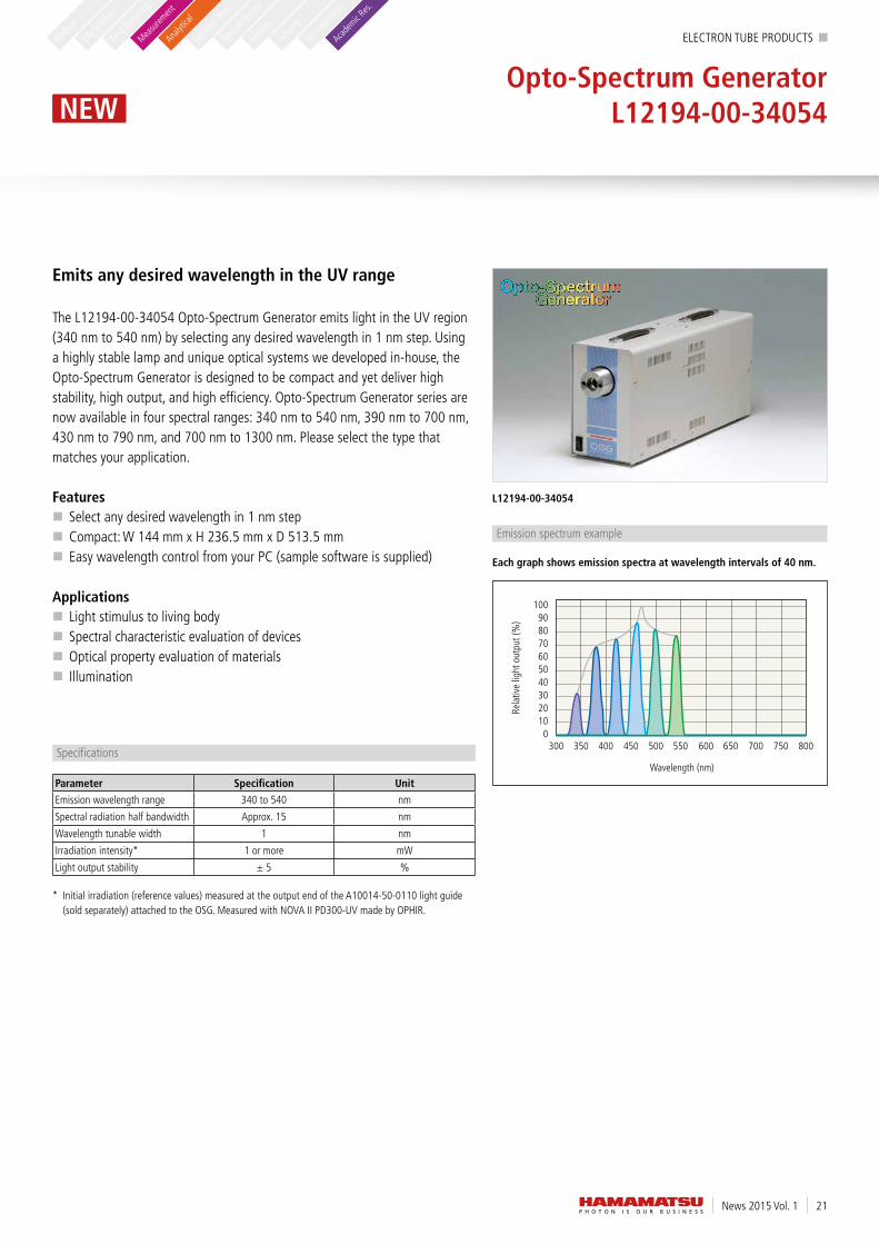
Emits any desired wavelength in the UV range
the L12194-00-34054 Opto-Spectrum Generator emits light in the Uv region (340 nm to 540 nm) by selecting any desired wavelength in 1 nm step. Using a highly stable lamp and unique optical systems we developed in-house, the Opto-Spectrum Generator is designed to be compact and yet deliver high stability, high output, and high efficiency. Opto-Spectrum Generator series are now available in four spectral ranges: 340 nm to 540 nm, 390 nm to 700 nm, 430 nm to 790 nm, and 700 nm to 1300 nm. Please select the type that matches your application.
Features � Select any desired wavelength in 1 nm step � Compact: w 144 mm x H 236.5 mm x D 513.5 mm � easy wavelength control from your PC (sample software is supplied)
Applications � Light stimulus to living body � Spectral characteristic evaluation of devices � Optical property evaluation of materials � Illumination
Each graph shows emission spectra at wavelength intervals of 40 nm.
L12194-00-34054
NEW
Specifications
Parameter Specification Unitemission wavelength range 340 to 540 nm
Spectral radiation half bandwidth Approx. 15 nm
wavelength tunable width 1 nm
Irradiation intensity* 1 or more mw
Light output stability ± 5 %
* Initial irradiation (reference values) measured at the output end of the A10014-50-0110 light guide (sold separately) attached to the OSG. Measured with nOvA II PD300-Uv made by OPHIr.
400350300 450 500 550 600 650 700 750 800
Wavelength (nm)
0
Rela
tive
light
out
put (
%)
102030405060708090
100
emission spectrum example
eLeCtrOn tUBe PrODUCtS
News 2015 Vol. 122
Specifications
Parameter Specification UnitSpectral response range 950 to 1,700 nm
Photocathode type InP/InGaAs -
Cathode quantum efficiency (typ.) at 1500 nm
2 %
Dark count* 5,000 s-1
ttS (fwHM) (typ.) 0.4 ns
* Supply voltage -800 v, at 25 deg. C.
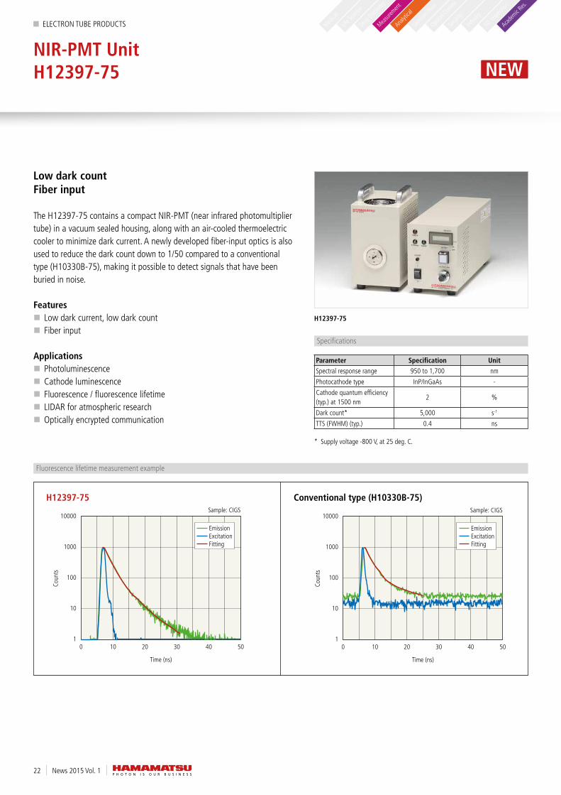
NIR-PMT Unit H12397-75
nD Inspe
ction
Indust
ry
Secu
rity
Optical
Comms
Semico
n Prod
.
Analyt
ical
Measur
emen
t
Drug Disc
overy
Life S
cienc
e
Medica
l
Academ
ic res.
Low dark count Fiber input
the H12397-75 contains a compact nIr-PMt (near infrared photomultiplier tube) in a vacuum sealed housing, along with an air-cooled thermoelectric cooler to minimize dark current. A newly developed fiber-input optics is also used to reduce the dark count down to 1/50 compared to a conventional type (H10330B-75), making it possible to detect signals that have been buried in noise.
Features � Low dark current, low dark count � fiber input
Applications � Photoluminescence � Cathode luminescence � fluorescence / fluorescence lifetime � LIDAr for atmospheric research � Optically encrypted communication
H12397-75
NEW
H12397-75 Conventional type (H10330B-75)
fluorescence lifetime measurement example
Sample: CIGS
0 101
10
100
1000
10000
20 30
Time (ns)
Coun
ts
40 50
EmissionExcitationFitting
Sample: CIGS
0 101
10
100
1000
10000
20 30
Time (ns)
Coun
ts
40 50
EmissionExcitationFitting
Sample: CIGS
0 101
10
100
1000
10000
20 30
Time (ns)
Coun
ts
40 50
EmissionExcitationFitting
Sample: CIGS
0 101
10
100
1000
10000
20 30
Time (ns)
Coun
ts
40 50
EmissionExcitationFitting
eLeCtrOn tUBe PrODUCtS
23News 2015 Vol. 1
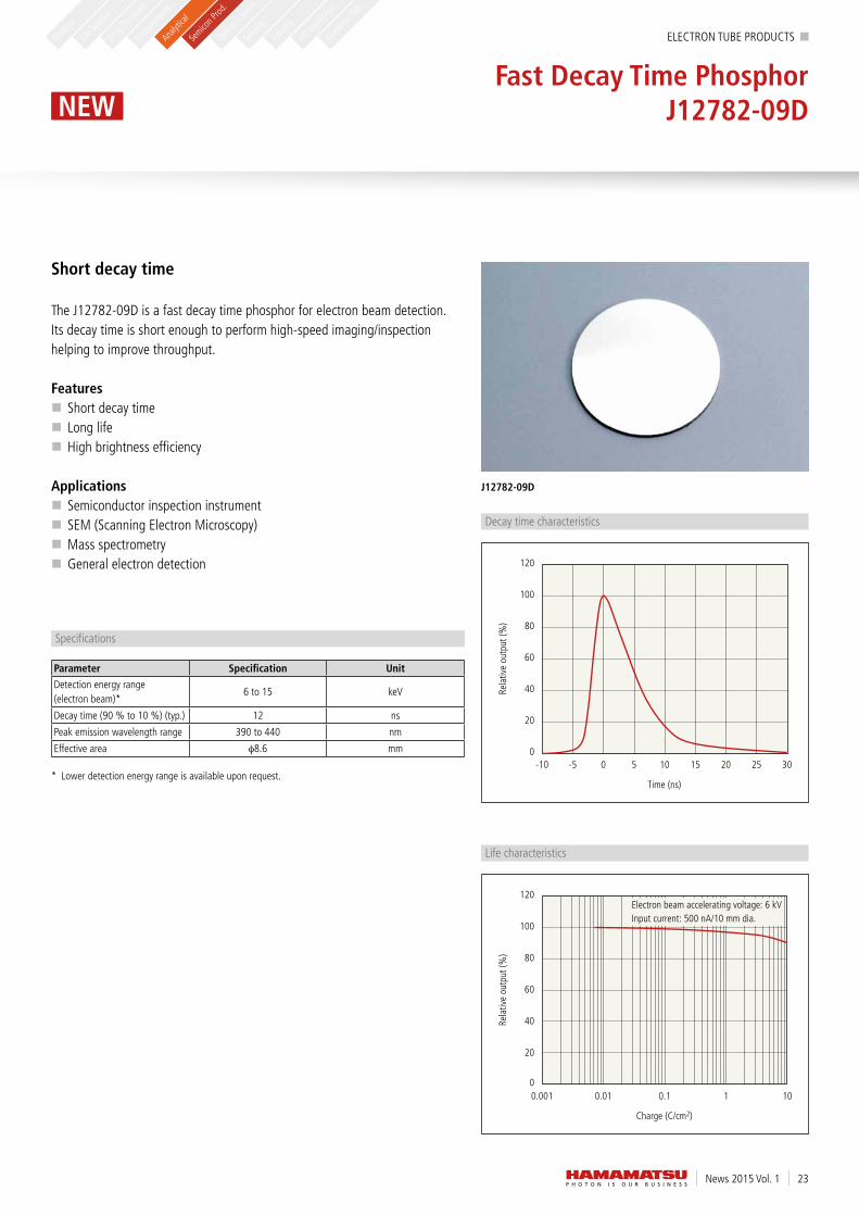
Decay time characteristics
Life characteristics
Specifications
Parameter Specification UnitDetection energy range (electron beam)*
6 to 15 kev
Decay time (90 % to 10 %) (typ.) 12 ns
Peak emission wavelength range 390 to 440 nm
effective area φ8.6 mm
* Lower detection energy range is available upon request.
Fast Decay Time Phosphor J12782-09D
Academ
ic res.
nD Inspe
ction
Indust
ry
Secu
rity
Optical
Comms
Semico
n Prod
.
Analyt
ical
Measur
emen
t
Drug Disc
overy
Life S
cienc
e
Medica
l
Short decay time
the J12782-09D is a fast decay time phosphor for electron beam detection. Its decay time is short enough to perform high-speed imaging/inspection helping to improve throughput.
Features � Short decay time � Long life � High brightness efficiency
Applications � Semiconductor inspection instrument � SeM (Scanning electron Microscopy) � Mass spectrometry � General electron detection
J12782-09D
NEW
-10 -5 0 5 10 20 3015 250
120
100
80
60
40
20
Time (ns)
Rela
tive
outp
ut (%
)
0.0010
20
40
60
80
100
120
0.01 0.1 1 10
Charge (C/cm2)
Rela
tive
outp
ut (%
)
Electron beam accelerating voltage: 6 kVInput current: 500 nA/10 mm dia.
-10 -5 0 5 10 20 3015 250
120
100
80
60
40
20
Time (ns)
Rela
tive
outp
ut (%
)
0.0010
20
40
60
80
100
120
0.01 0.1 1 10
Charge (C/cm2)
Rela
tive
outp
ut (%
)
Electron beam accelerating voltage: 6 kVInput current: 500 nA/10 mm dia.
SYSteMS PrODUCtS
News 2015 Vol. 124
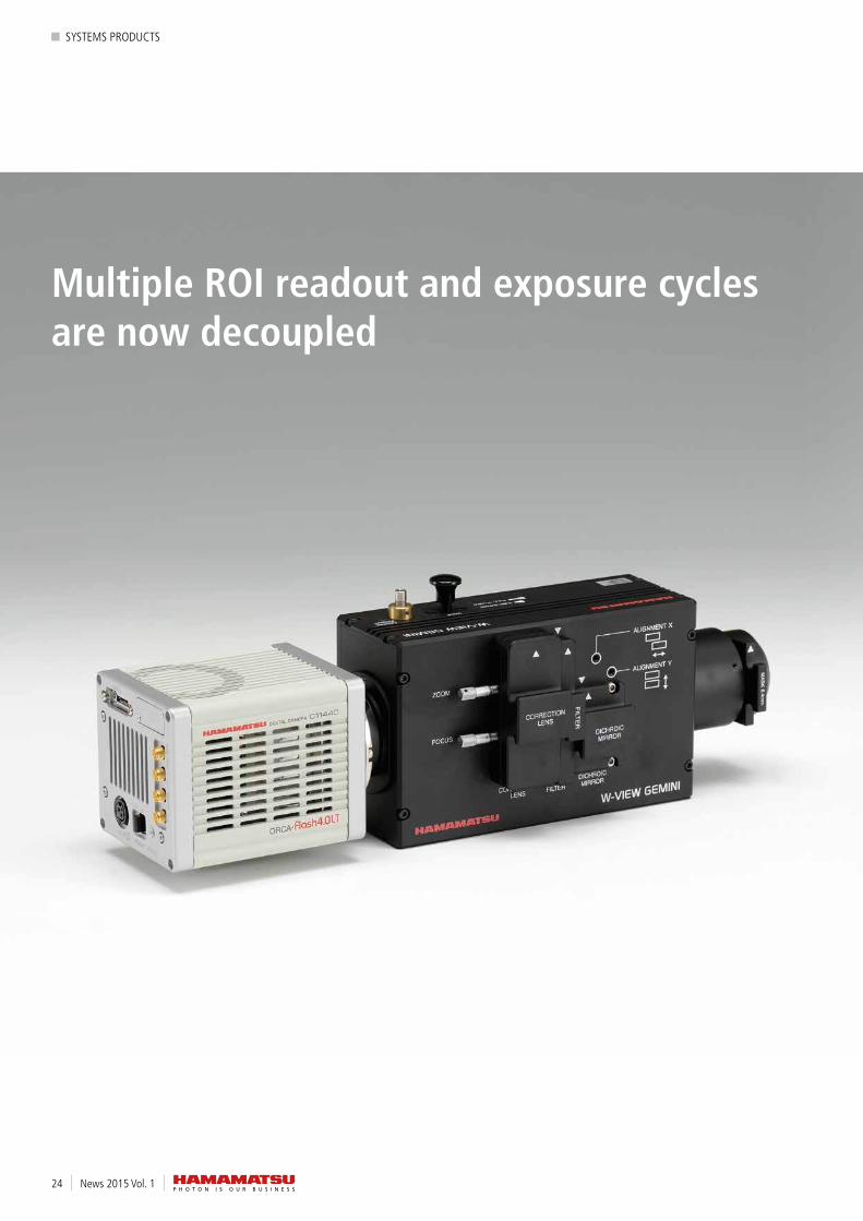
Multiple ROI readout and exposure cyclesare now decoupled
SYSteMS PrODUCtS
25News 2015 Vol. 1
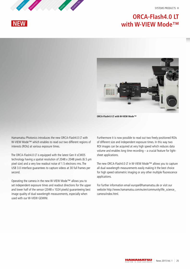
ORCA-Flash4.0 LT with W-VIEW Mode™NEW
Hamamatsu Photonics introduces the new OrCA-flash4.0 Lt with w-vIew Mode™ which enables to read out two different regions of interests (rOIs) at various exposure times.
the OrCA-flash4.0 Lt is equipped with the latest Gen II sCMOS technology having a spatial resolution of 2048 x 2048 pixels (6.5 µm pixel size) and a very low readout noise of 1.5 electrons rms. the USB 3.0 interface guarantees to capture videos at 30 full frames per second.
Operating the camera in the new w-vIew Mode™ allows you to set indepen dent exposure times and readout directions for the upper and lower half of the sensor (2048 x 1024 pixels) guaranteeing best image quality of dual wavelength measurements, especially when used with our w-vIew GeMInI.
furthermore it is now possible to read out two freely positioned rOIs of different size and independent exposure times. In this way two rOI images can be acquired at very high speed which reduces data volume and enables long time recording – a crucial feature for light-sheet applications.
the new OrCA-flash4.0 Lt in w-vIew Mode™ allows you to capture all dual wavelength measurements easily making it the best choice for high speed ratiometric imaging or any other multiple fluorescence applications.
for further information email [email protected] or visit our website http://www.hamamatsu.com/eu/en/community/life_science_camera/index.html.
ORCA-Flash4.0 LT with W-VIEW Mode™
Academ
ic res.
nD Inspe
ction
Indust
ry
Secu
rity
Optical
Comms
Semico
n Prod
.
Analyt
ical
Measur
emen
t
Drug Disc
overy
Life S
cienc
e
Medica
l

SYSteMS PrODUCtS
News 2015 Vol. 126
NanoZoomer-SQ Digital Slide Scanner C13140-21
nD Inspe
ction
Indust
ry
Secu
rity
Optical
Comms
Semico
n Prod
.
Analyt
ical
Measur
emen
t
Drug Disc
overy
Life S
cienc
e
Medica
l
Academ
ic res.
The easy-to-use, affordable and high quality desktop scanner for whole slide imaging
nanoZoomer-SQ is Hamamatsu’s new desktop single slide scanner for creating whole slide images of single tissue slides. Its very compact size makes it suitable even for the smallest lab, while maintaining the well-renowned reliability and robustness of Hamamatsu whole slide scanners.
Features � Desktop and lightweight � Affordable � High quality and reliable � easy operation
Applications � teleconsultation � education & training � Image analysis
C13140-21
NEW
Has the feel of a microscope, with the possibility to view a whole tissue section, as well as a region of interest
A push of the start button on the scanner is all that is required to create a high quality digital slide.
Easy operation
SYSteMS PrODUCtS
27News 2015 Vol. 1
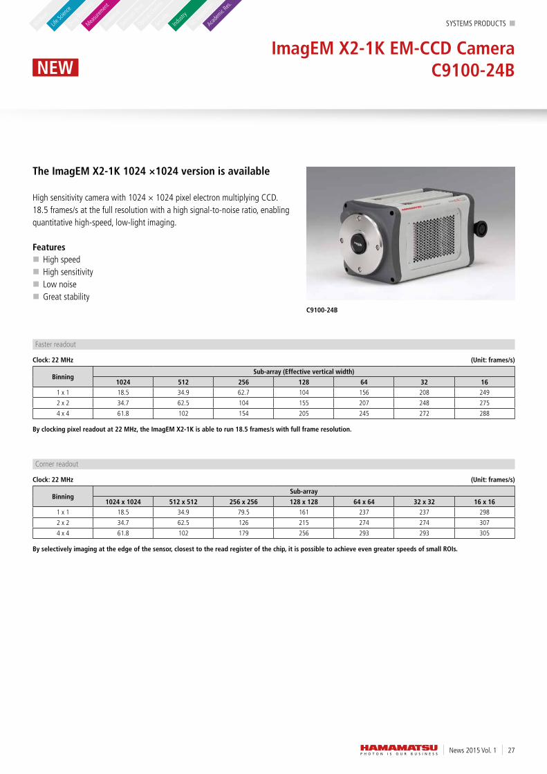
ImagEM X2-1K EM-CCD Camera C9100-24B
The ImagEM X2-1K 1024 ×1024 version is available
High sensitivity camera with 1024 × 1024 pixel electron multiplying CCD. 18.5 frames/s at the full resolution with a high signal-to-noise ratio, enabling quantitative high-speed, low-light imaging.
Features � High speed � High sensitivity � Low noise � Great stability
C9100-24B
Academ
ic res.
nD Inspe
ction
Indust
ry
Secu
rity
Optical
Comms
Semico
n Prod
.
Analyt
ical
Measur
emen
t
Drug Disc
overy
Life S
cienc
e
Medica
l
NEW
BinningSub-array (Effective vertical width)
1024 512 256 128 64 32 161 x 1 18.5 34.9 62.7 104 156 208 249
2 x 2 34.7 62.5 104 155 207 248 275
4 x 4 61.8 102 154 205 245 272 288
faster readout
Clock: 22 MHz
By clocking pixel readout at 22 MHz, the ImagEM X2-1K is able to run 18.5 frames/s with full frame resolution.
(Unit: frames/s)
(Unit: frames/s)
BinningSub-array
1024 x 1024 512 x 512 256 x 256 128 x 128 64 x 64 32 x 32 16 x 161 x 1 18.5 34.9 79.5 161 237 237 298
2 x 2 34.7 62.5 126 215 274 274 307
4 x 4 61.8 102 179 256 293 293 305
Corner readout
Clock: 22 MHz
By selectively imaging at the edge of the sensor, closest to the read register of the chip, it is possible to achieve even greater speeds of small ROIs.
LASer PrODUCtS
News 2015 Vol. 128
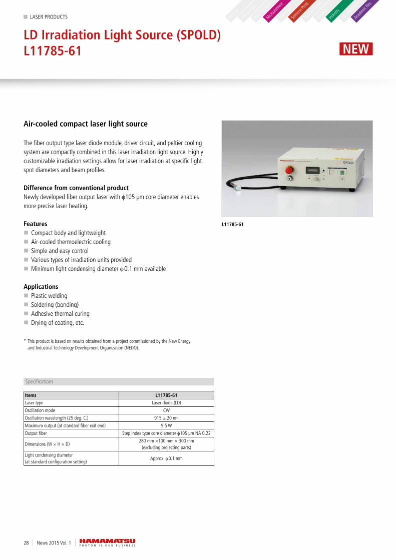
LD Irradiation Light Source (SPOLD) L11785-61
Air-cooled compact laser light source
the fiber output type laser diode module, driver circuit, and peltier cooling system are compactly combined in this laser irradiation light source. Highly customizable irradiation settings allow for laser irradiation at specific light spot diameters and beam profiles. Difference from conventional product newly developed fiber output laser with φ105 µm core diameter enables more precise laser heating.
Features � Compact body and lightweight � Air-cooled thermoelectric cooling � Simple and easy control � various types of irradiation units provided � Minimum light condensing diameter φ0.1 mm available
Applications
� Plastic welding � Soldering (bonding) � Adhesive thermal curing � Drying of coating, etc.
* this product is based on results obtained from a project commissioned by the new energy and Industrial technology Development Organization (neDO).
L11785-61
Academ
ic res.
nD Inspe
ction
Indust
ry
Secu
rity
Optical
Comms
Semico
n Prod
.
Analyt
ical
Measur
emen
t
Drug Disc
overy
Life S
cienc
e
Medica
l
NEW
Specifications
Items L11785-61Laser type Laser diode (LD)
Oscillation mode Cw
Oscillation wavelength (25 deg. C.) 915 ± 20 nm
Maximum output (at standard fiber exit end) 9.5 w
Output fiber Step index type core diameter φ105 µm nA 0.22
Dimensions (w × H × D)280 mm ×100 mm × 300 mm
(excluding projecting parts)
Light condensing diameter (at standard configuration setting)
Approx. φ0.1 mm
LASer PrODUCtS
29News 2015 Vol. 1
Super Luminescent Diode (SLD) L12856-04
Academ
ic res.
nD Inspe
ction
Indust
ry
Secu
rity
Optical
Comms
Semico
n Prod
.
Analyt
ical
Measur
emen
t
Drug Disc
overy
Life S
cienc
e
Medica
l
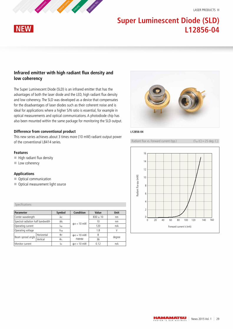
Infrared emitter with high radiant flux density and low coherency
the Super Luminescent Diode (SLD) is an infrared emitter that has the advantages of both the laser diode and the LeD, high radiant flux density and low coherency. the SLD was developed as a device that compensates for the disadvantages of laser diodes such as their coherent noise and is ideal for applications where a higher S/n ratio is essential, for example in optical measurements and optical communications. A photodiode chip has also been mounted within the same package for monitoring the SLD output.
Difference from conventional product:this new series achieves about 3 times more (10 mw) radiant output power of the conventional L8414 series.
Features � High radiant flux density � Low coherency
Applications � Optical communication � Optical measurement light source
L12856-04
0 20 40 60 80 100 1200
2
6
8
10
12
14
16
Forward current If (mA)
Radi
ant f
lux φ
e (m
W)
140
4
160
radiant flux vs. forward current (typ.) (top (C) = 25 deg. C.)
NEW
Specifications
Parameter Symbol Condition Value UnitCenter wavelength λc
φe = 10 mw
830 ± 10 nm
Spectral radiation half bandwidth Δλ 10 nm
Operating current Iop 120 mA
Operating voltage vop 1.8 v
Beam spread angleHorizontal θ// φe = 10 mw
fwHM8
degreevertical θ⊥ 36
Monitor current Im φe = 10 mw 0.12 mA

News 2015 Vol. 130
Global Exhibitions 2015
USA
May 2015
Radiation Detection ConferenceMay 19-21 2015, fairfax, vA
ASMSMay 31-June 5 2015, Baltimore, MD
June 2015
Digital Pathology Congress USAJune 22-23 2015, San Diego, CA
July 2015
Ion Channel RetreatJuly 6-8 2015, vancouver, Canada
SEMICON WestJuly 14-16 2015, San francisco, CA
August 2015
Optics and PhotonicsAug 11-13 2015, San Diego, CA
October 2015
IEEE Photonics ConferenceOct 4-8 2015, reston, vA
Nuclear Science SymposiumOct 31-Nov 1 2015, San Diego, CA
eUrOPe
May 2015
PSMR 2015May 17-20 2015, La Biodola, Italy
Sensor und TestMay 19-21 2015, nuremberg, Germany
IOP Nuclear Physics in AstrophysicsMay 19-21 2015, York, england
ELMIMay 19-22 2015, Sitges, Spain
National Electronics Week (NEW) South AfricaMay 20 2015, Durban, South Africa
Vårmöte i Patologi May 20-22 2015, Örebro, Sweden
PhotoDet 2015July 6-9 2015, troitsk, russia
UK Space ConferenceJuly 14-15 2015, Liverpool, england
IVAS 2015July 14-17 2015, Mezzocorona (tn), Italy
8th International Conference – PCRRTJuly 16-18 2015, London, england
EPS-HEP 2015July 22-29 2015, vienna, Austria
Reflections on the Atomic NucleusJuly 28-29 2015, Liverpool, england
ICRC – The Astroparticle Physics ConferenceJuly 30-Aug 6 2015, the Hague, netherlands
August 2015
GCFs SMLMS'15 – 5th Single Molecule Localization Microscopy SymposiumAug 26-28 2015, Bordeaux, france
September 2015
ELRIG: Drug DiscoverySept 2-3 2015, telford, england
ECP – 27th European Congress of PathologySept 5-9 2015, Belgrad, Serbia
TAUP 2015Sept 7-11 2015, torino, Italy
XXXVI Convegno della Divisione di Chimica Organica-CDCO 2015Sept 13-17 2015, Bologna, Italy
14th Conference on Methods and Applications of FluorescenceSept 13-16 2015, wuerzburg, Germany
Single-Molecule Microscopy and SpectroscopySept 14-16 2015, London, england
Gemeinschaftsstand Bayern Innovativ IAASept 15-18 2015, frankfurt, Germany
BMSS Annual MeetingSept 16-17 2015, Birmingham, england
4th Champalimaud Neuroscience SymposiumSept 16-19 2015, Lisbon, Portugal
7th Size-Strain ConferenceSept 21-24 2015, Oxford, england
ENOVA ParisSept 22-24 2015, Paris, france
MipTecSept 22-24 2015, Basel, Switzerland
October 2015
EMBL – Seeing is BelievingOct 6-10 2015, Heidelberg, Germany
41. Jahrestagung – Gesellschaft für Neonatologie und Pädiatrische IntensivmedizinMay 21-23 2015, Stuttgart, Germany
XIII Pisa Meeting on Advanced DetectorsMay 23-30 2015, La Biodola, Italy
99. Jahrestagung – dt. Gesellschaft für PathologyMay 28-31 2015, frankfurt, Germany
ESA-EuroanaesthesiaMay 30-June 1 2015, Berlin, Germany
June 2015
6th Workshop on Nanotube Optics and Nanospectroscopy June 1-4 2015, Kloster Banz, Germany
Northern Optics 2015June 2-4 2015, Lappeenranta, finland
EPHJ-EPMT-SMTJune 2-5 2015, Lausanne, Switzerland
Photonex Scotland RoadshowJune 3 2015, Glasgow, Scotland
Photonics Event June 3-4 2015, veldhoven, netherlands
Photon Diag 2015June 8-10 2015, trieste, Italy
ESPNICJune 10-13 2015, vilnius, Lithuania
Automotive Interiors ExpoJune 16-18 2015, Stuttgart, Germany
Digital Industrial Radiology & Computed TomographyJune 22-25 2015, Ghent, Belgium
Laser-World of PhotonicsJune 22-25 2015, Munich, Germany
Dublin Pathology 2015June 23-25 2015, Dublin, Ireland
Imaging the CellJune 24 2015, Bordeaux, france
EACTAJune 24-26 2015, Gothenburg, Sweden
CYTO June 27-30 2015, Glasgow, ScotlandEuropean Zebrafish Meeting EZM 2015 June 28-July 2 2015, Oslo, norway
Microscience Microscopy Congress (MMC) June 29-July 2 2015, Manchester, england
July 2015
40th FEBS Congress – the Biochemical Basis of LifeJuly 4-9 2015, Berlin, Germany
Lightsheet Fluorescence Microscopy 2015July 5-8 2015, Genova, Italy
31News 2015 Vol. 1
Hamamatsu Photonics K.K.Sales Offices
JAPAN:HAMAMATSU PHOTONICS K.K.325-6, Sunayama-cho, naka-kuHamamatsu City, Shizuoka Pref. 430-8587, Japantelephone: (81)53 452 2141, fax: (81)53 456 7889
China:HAMAMATSU PHOTONICS (CHINA) Co., Ltd1201 tower B, Jiaming Center, 27 DongsanhuanBeilu, Chaoyang District, Beijing 100020, Chinatelephone: (86)10 6586 6006, fax: (86)10 6586 2866e-mail: [email protected]
USA:HAMAMATSU CORPORATIONMain Office:360 foothill roadBridgewater, nJ 08807, U.S.A.telephone: (1)908 231 0960, fax: (1)908 231 1218e-mail: [email protected]
Western U.S.A. Office:Suite 200 & Suite 110, 2875 Moorpark Avenue,San Jose, CA 95128, U.S.A.telephone: (1)408 261 2022, fax: (1)408 261 2522e-mail: [email protected]
United Kingdom, South Africa:HAMAMATSU PHOTONICS UK LIMITEDMain Office:2 Howard Court, 10 tewin road, welwyn Garden City,Hertfordshire, AL7 1Bw, United Kingdomtelephone: (44)1707 294888, fax: (44)1707 325777e-mail: [email protected]
South Africa Office:PO Box 1112Buccleuch 2066Johannesburg, South Africatelephone/fax: (27)11 8025505
France, Belgium, Switzerland, Spain, Portugal:HAMAMATSU PHOTONICS FRANCE S.A.R.L.Main Office: 19, rue du Saule trapu, Parc du Moulin de Massy,91882 Massy Cedex, francetelephone: (33)1 69 53 71 00, fax: (33)1 69 53 71 10e-mail: [email protected]
Swiss Office:Dornacherplatz 74500 Solothurn, Switzerlandtelephone: (41)32 625 60 60, fax: (41)32 625 60 61e-mail: [email protected]
Belgian Office:Axisparc technology,7, rue Andre DumontB-1435 Mont-Saint-Guibert, Belgiumtelephone: (32)10 45 63 34, fax: (32)10 45 63 67e-mail: [email protected]
Spanish Office:C. Argenters, 4 edif 2Parque tecnológico del vallése-08290 Cerdanyola, (Barcelona) Spaintelephone: (34)93 582 44 30, fax: (34)93 582 44 31e-mail: [email protected]
Germany, Denmark, Netherlands, Poland:HAMAMATSU PHOTONICS DEUTSCHLAND GmbHMain Office: Arzbergerstr. 10,D-82211 Herrsching am Ammersee, Germanytelephone: (49)8152 375 0, fax: (49)8152 265 8e-mail: [email protected]
Danish Office:Lautruphoj 1-3DK-2750 Ballerup, Denmarktelephone: (45)70 20 93 69, fax: (45)44 20 99 10e-mail: [email protected]
Netherlands Office:televisieweg 2nL-1322 AC Almere, the netherlandstelephone: (31)36 5405384, fax: (31)36 5244948e-mail: [email protected]
Poland Office:02-525 warsaw,8 St. A. Boboli Str., Polandtelephone: (48)22 646 0016, fax: (48)22 646 0018e-mail: [email protected]
North Europe and CIS:HAMAMATSU PHOTONICS NORDEN ABMain Office: torshamnsgatan 35Se-16440 Kista, Swedentelephone: (46)8 509 031 00, fax: (46)8 509 031 01e-mail: [email protected]
Russian Office:11, Chistoprudny Boulevard, Building 1,rU-101000, Moscow, russia telephone: (7)495 258 85 18, fax: (7)495 258 85 19e-mail: [email protected]
Italy:HAMAMATSU PHOTONICS ITALIA S.R.L.Main Office: Strada della Moia, 1 int. 620020 Arese, (Milano), Italytelephone: (39)02 93581733, fax: (39)02 93581741e-mail: [email protected]
Rome Office:viale Cesare Pavese, 435,00144 roma, Italytelephone: (39)06 50513454, fax: (39)06 50513460e-mail: [email protected]
Impressum
Hamamatsu Photonics News
Publisher and copyright:HAMAMATSU PHOTONICS K.K.325-6, Sunayama-cho, naka-kuHamamatsu City Shizuoka Pref. 430-8587, Japantelephone: (81)53 452 2141fax: (81)53 456 7889http://[email protected]
Editor and responsible for content:Hiroaki fukuoka
Publishing frequency:Bi-annual, Date of this issue May 2015
Graphics and realisation:SInnIQ technologiewerbung Ltd.www.sinniq.com
Printing:Mühlbauer Druck GmbH
Copyright:reproduction in part or whole only allowed with our written permission. All rights reserved.
Information in this catalogue is believed to be reliable. However, no responsibility is assumed for possible inaccuracies or omissions. Specifications are subject to change without notice. no patent rights are granted to any of the circuits described herein.
© 2015 Hamamatsu Photonics K.K.

Hamamatsu News – now also online:
www.hamamatsu-news.com
www.hamamatsu.com


